EP4101811A1 - Hydrogen production cell - Google Patents
Hydrogen production cell Download PDFInfo
- Publication number
- EP4101811A1 EP4101811A1 EP22159853.5A EP22159853A EP4101811A1 EP 4101811 A1 EP4101811 A1 EP 4101811A1 EP 22159853 A EP22159853 A EP 22159853A EP 4101811 A1 EP4101811 A1 EP 4101811A1
- Authority
- EP
- European Patent Office
- Prior art keywords
- photocatalyst
- ferroelectric
- layer
- electrode
- hydrogen production
- Prior art date
- Legal status (The legal status is an assumption and is not a legal conclusion. Google has not performed a legal analysis and makes no representation as to the accuracy of the status listed.)
- Pending
Links
Images



Classifications
-
- C—CHEMISTRY; METALLURGY
- C01—INORGANIC CHEMISTRY
- C01B—NON-METALLIC ELEMENTS; COMPOUNDS THEREOF; METALLOIDS OR COMPOUNDS THEREOF NOT COVERED BY SUBCLASS C01C
- C01B3/00—Hydrogen; Gaseous mixtures containing hydrogen; Separation of hydrogen from mixtures containing it; Purification of hydrogen; Reversible storage of hydrogen
- C01B3/02—Production of hydrogen; Production of gaseous mixtures containing hydrogen
- C01B3/04—Production of hydrogen; Production of gaseous mixtures containing hydrogen by decomposition of inorganic compounds
- C01B3/042—Decomposition of water
-
- C—CHEMISTRY; METALLURGY
- C25—ELECTROLYTIC OR ELECTROPHORETIC PROCESSES; APPARATUS THEREFOR
- C25B—ELECTROLYTIC OR ELECTROPHORETIC PROCESSES FOR THE PRODUCTION OF COMPOUNDS OR NON-METALS; APPARATUS THEREFOR
- C25B1/00—Electrolytic production of inorganic compounds or non-metals
- C25B1/01—Products
- C25B1/02—Hydrogen or oxygen
- C25B1/04—Hydrogen or oxygen by electrolysis of water
- C25B1/044—Hydrogen or oxygen by electrolysis of water producing mixed hydrogen and oxygen gas, e.g. Brown's gas [HHO]
-
- C—CHEMISTRY; METALLURGY
- C25—ELECTROLYTIC OR ELECTROPHORETIC PROCESSES; APPARATUS THEREFOR
- C25B—ELECTROLYTIC OR ELECTROPHORETIC PROCESSES FOR THE PRODUCTION OF COMPOUNDS OR NON-METALS; APPARATUS THEREFOR
- C25B9/00—Cells or assemblies of cells; Constructional parts of cells; Assemblies of constructional parts, e.g. electrode-diaphragm assemblies; Process-related cell features
- C25B9/50—Cells or assemblies of cells comprising photoelectrodes; Assemblies of constructional parts thereof
-
- C—CHEMISTRY; METALLURGY
- C25—ELECTROLYTIC OR ELECTROPHORETIC PROCESSES; APPARATUS THEREFOR
- C25B—ELECTROLYTIC OR ELECTROPHORETIC PROCESSES FOR THE PRODUCTION OF COMPOUNDS OR NON-METALS; APPARATUS THEREFOR
- C25B9/00—Cells or assemblies of cells; Constructional parts of cells; Assemblies of constructional parts, e.g. electrode-diaphragm assemblies; Process-related cell features
- C25B9/60—Constructional parts of cells
- C25B9/65—Means for supplying current; Electrode connections; Electric inter-cell connections
-
- C—CHEMISTRY; METALLURGY
- C25—ELECTROLYTIC OR ELECTROPHORETIC PROCESSES; APPARATUS THEREFOR
- C25B—ELECTROLYTIC OR ELECTROPHORETIC PROCESSES FOR THE PRODUCTION OF COMPOUNDS OR NON-METALS; APPARATUS THEREFOR
- C25B9/00—Cells or assemblies of cells; Constructional parts of cells; Assemblies of constructional parts, e.g. electrode-diaphragm assemblies; Process-related cell features
- C25B9/70—Assemblies comprising two or more cells
-
- Y—GENERAL TAGGING OF NEW TECHNOLOGICAL DEVELOPMENTS; GENERAL TAGGING OF CROSS-SECTIONAL TECHNOLOGIES SPANNING OVER SEVERAL SECTIONS OF THE IPC; TECHNICAL SUBJECTS COVERED BY FORMER USPC CROSS-REFERENCE ART COLLECTIONS [XRACs] AND DIGESTS
- Y02—TECHNOLOGIES OR APPLICATIONS FOR MITIGATION OR ADAPTATION AGAINST CLIMATE CHANGE
- Y02E—REDUCTION OF GREENHOUSE GAS [GHG] EMISSIONS, RELATED TO ENERGY GENERATION, TRANSMISSION OR DISTRIBUTION
- Y02E60/00—Enabling technologies; Technologies with a potential or indirect contribution to GHG emissions mitigation
- Y02E60/30—Hydrogen technology
- Y02E60/36—Hydrogen production from non-carbon containing sources, e.g. by water electrolysis
-
- Y—GENERAL TAGGING OF NEW TECHNOLOGICAL DEVELOPMENTS; GENERAL TAGGING OF CROSS-SECTIONAL TECHNOLOGIES SPANNING OVER SEVERAL SECTIONS OF THE IPC; TECHNICAL SUBJECTS COVERED BY FORMER USPC CROSS-REFERENCE ART COLLECTIONS [XRACs] AND DIGESTS
- Y02—TECHNOLOGIES OR APPLICATIONS FOR MITIGATION OR ADAPTATION AGAINST CLIMATE CHANGE
- Y02P—CLIMATE CHANGE MITIGATION TECHNOLOGIES IN THE PRODUCTION OR PROCESSING OF GOODS
- Y02P20/00—Technologies relating to chemical industry
- Y02P20/10—Process efficiency
- Y02P20/133—Renewable energy sources, e.g. sunlight
Definitions
- the present invention relates to a hydrogen production cell and, more particularly, to technology effectively applied to hydrogen production cells for producing hydrogen through water splitting by reaction induced by light energy.
- P2G Power to Gas
- Photocatalyst is drawing attention which enables generation of hydrogen from water and solar energy and storage of energy as hydrogen. Suggestions about such photocatalyst are described, for example, in International Publication No. WO2017/164191 , Japanese Unexamined Patent Application Publications Nos. 2008-104899 and 2017-155332 , and the like.
- a p-n junction photocatalyst with p-type and n-type semiconductors joined together has been studied.
- a junction between the p-type semiconductor and the n-type semiconductor is made in order to create a structure that facilitates spatial separation between electrons and positive holes.
- Necessity for making such a p-n junction is that appropriate doping is performed to make individually the p-type semiconductor and the n-type semiconductor.
- oxide semiconductor with stable structure is apt to become n-type. Because of this, it has been difficult to find out a material capable of making a p-n conjunction.
- a ferroelectric substance is placed to face the photocatalyst, the ferroelectric substance creating a potential gradient with respect to the photocatalyst.
- a hydrogen production cell which uses a photocatalyst capable of effectively using light energy for a desired reaction such as a water decomposition reaction and/or the like.
- a water decomposition reaction by a photocatalytic reaction and a water electrolysis reaction caused by use of a solar cell are expressed in general by reaction a formula (1) as follows.
- a junction between a p-type semiconductor and an n-type semiconductor is made in order to create a structure that facilitates spatial separation between electrons and positive holes.
- Necessity for making such a p-n junction is that appropriate doping is performed to make individually the p-type semiconductor and the n-type semiconductor.
- materials for oxide semiconductors and the like some of materials are difficult to be made into a p-type semiconductors, and thus no p-type semiconductor may be obtained.
- a structure by which spatial charge separation is promoted is made without individually making the p-type semiconductor and the n-type semiconductor, in order to provide separation between electrons and positive holes and inhibition of recombination thereof.
- the surface area of a semiconductor in which the exited electrons and positive holes are utilized is increased in order to increase the reaction efficiency of water and/or a compound as fuel obtained by reduction of carbon dioxide, for use in hydrogen production. This makes it possible to provide a hydrogen production cell using a photocatalytic semiconductor which is capable of effectively using light energy for a desired reaction such as a water decomposition reaction.
- the present invention provides a structure that enables improved efficiency of production of hydrogen and oxygen through water splitting by inhibiting recombination of carriers which are produced by irradiating, with light, a photocatalytic semiconductor of thin film or bulk.
- a spontaneously polarized ferroelectric material and a semiconductor material exhibiting photocatalytic effects are stacked one on top of another.
- an effective electric field is applied to the photocatalytic semiconductor (i.e., create a potential gradient with respect to the photocatalytic semiconductor) to promote the spatial separation between electrons and positive holes and inhabit recombination of carriers.
- the photocatalytic effects in proximity to the ferroelectric may be enhanced. This obviates the necessity of achieving separately material formations for a p-type semiconductor and an n-type semiconductor, and thus the tendency of electrons and positive holes to recombine may be reduced. Therefore, a stable hydrogen production cell is provided.
- Fig. 1 is a cross-sectional view illustrating a first example configuration of a photocatalyst electrode according to the embodiments.
- Fig. 2 is a diagram illustrating the relationship between electric field and polarization of a ferroelectric.
- a photocatalyst electrode 1 used in a hydrogen production cell has a substrate 10, an electrode 20 placed in contact with the top face of the substrate 10, a ferroelectric layer 30 placed in contact with the top face of the electrode 20, a semiconductor photocatalyst layer 40 placed in contact with the tope face of the ferroelectric layer 30, and promoters 50 adhering to the surface of the semiconductor photocatalyst layer 40.
- the promoters 50 are not an essential configuration, but providing the promoters 50 may yield about an improvement in photocatalytic reaction rate.
- the substrate 10 may be formed from, for example, quartz.
- the electrode (also referred to as an "electrode layer") 20 may be formed from, for example, Pt (platinum).
- the electrode 20 may translate to an electrode layer.
- the ferroelectric layer 30 may be formed by use of, for example, BaTiO 3 , Pb(Zr,Ti)O 3 , LiNbO 3 , LiTaO 3 , YbFe 2 O 4 and/or the like.
- multiferroic materials with magnetization at room temperature such as Pb 3 TeMn 3 P 2 O 14 may be used. The use of the multiferroic materials enables control on the direction of electric polarization by magnetic fields.
- the semiconductor photocatalyst layer 40 may be formed by use of a material selected from the group of, for example, ATa 2 O 6 (A: Sr, Ba), Sr 2 Nb 2 O 7 , Sr 2 Ta 2 O 7 , ATa 2 O 6 (A: Ca, Sr, Ba), K 3 Ta 3 Si 2 O13, ATaO 3 (A:Li,Na,K), AgTaO 3 , NaTaO 3 , K 2 LnTa 5 O 15 , K 3 Ta 3 B 2 O 12 , Cs 2 Nb 4 O 11 , Ba 5 Nb 4 O 15 , ATa 3 O 8 (A:Rb, Cs), Cs 4 Ta 10 O 27 , Cs 6 Ta 16 O 43 , ZnS, NaInS 2 , SrTiO 3 , AgGaS2, CuGaS2, CuInS 2 -AgInS 2 -ZnS, CuInS2-AgInS2, A 2 Ti 2 O 7 (A: Sc, Y, La
- a material resulting from substitution of nitrogen or sulfur for a portion of oxygen in the above materials may be used for the semiconductor photocatalyst layer 40.
- the materials mentioned above are illustrative only, and any semiconductor material other than the above may be used for the semiconductor photocatalyst layer 40.
- the promoters 50 include Pt (platinum), Ru (ruthenium), Rh (rhodium), Cr (chromium), and/or the like.
- the ferroelectric layer 30 and the semiconductor photocatalyst layer 40 are stacked one on top of another. Because of this, the ferroelectric layer 30 is placed to face the semiconductor photocatalyst layer 40. An electric field is applied from the electrode 20 to the ferroelectric layer 30, so that the ferroelectric layer 30 may change the direction of polarization. As illustrated in Fig. 1 , the ferroelectric layer 30 is designed such that electric polarization 35 is in a direction perpendicular to the top face of the substrate 10 (in the upward direction in the example). Typically, the relationship between the ferroelectric electric polarization 35 and an electric field exhibits hysteresis characteristics as illustrated in Fig. 2 .
- an electric field is applied to orient the polarization to the same direction, the state of spontaneous polarization 35 is maintained.
- an electric field is applied to the semiconductor photocatalyst layer 40 located close to the ferroelectric layer 30.
- an effective electric field is applied to the semiconductor photocatalyst layer 40, that is, a potential gradient is created with respect to the semiconductor photocatalyst layer 40 to promote the spatial separation between electrons and positive holes and inhabit recombination of carriers.
- the photocatalytic effects may be enhanced in the semiconductor photocatalyst layer 40 in proximity to the ferroelectric layer 30.
- the photocatalyst electrode 1 is immersed in an aqueous medium stored in the hydrogen production cell, and the photocatalyst electrode 1 is irradiated with, for example, solar light.
- the light irradiation allows the semiconductor photocatalyst layer 40 to produce carriers (electrons and positive holes).
- the ferroelectric layer 30 is electrically polarized, and an electric field (potential gradient) is applied to the semiconductor photocatalyst layer 40 by the electric polarization.
- an electric field potential gradient
- spatial charge separation between the electrons and positive holes generated by the light irradiation is induced in the semiconductor photocatalyst layer 40, and recombination of the electrons and the positive holes is inhibited.
- the electron and the positive holes after the spatial charge separation within the semiconductor photocatalyst layer 40 initiate a decomposition reaction of the aqueous medium with high efficiency, and thus hydrogen and oxygen are generated.
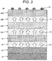
- Fig. 3 is a cross-sectional view illustrating a second example configuration of a photocatalyst electrode according to the embodiments.
- the difference between a photocatalyst electrode 1A illustrated in Fig. 3 and the photocatalyst electrode 1 in Fig. 1 is that, in the photocatalyst electrode 1A, a ferroelectric layer 30A, a semiconductor photocatalyst layer 40A, a ferroelectric layer 30B, and a semiconductor photocatalyst layer 40B are stacked in this order on a semiconductor photocatalyst layer 40 in a multilayer fashion.
- the number of interfaces between the semiconductor photocatalyst layer (40, 40A, 40B) and the ferroelectric layer (30, 30A, 30B) may be increased. Because of charge bias arising in proximity to the interface between the semiconductor photocatalyst layer and the ferroelectric layer, one of both the electrons and the positive holes is collected according to the direction of the polarization 35 of the ferroelectric layer (30, 30A, 30B). Therefore, the charges are particularly spatially separated in proximity to the interface. Thus, the number of electrons or positive holes in the photocatalyst electrode 1A in Fig. 3 may be increased as compared with that in the photocatalyst electrode 1 in Fig. 1 .
- a plurality of sets of the ferroelectric layer (30, 30A, 30B) and the semiconductor photocatalyst layer (40, 40A, 40B) are provided, so that it is possible to increase the surface area (the interface area) of the semiconductor photocatalyst layer (40, 40A, 40B) in which the electrons and positive holes excited by the light irradiation are used. This enables an increase in reaction efficiency of a compound used in hydrogen production.
- Fig. 4 is a cross-sectional view illustrating a third example configuration of a photocatalyst electrode according to the embodiments.
- the difference between a photocatalyst electrode 1B illustrated in Fig. 4 and the photocatalyst electrode 1 in Fig. 1 is that, in the photocatalyst electrode 1B, the electrode 20, the ferroelectric layer 30, and the semiconductor catalyst layer 40 are designed as a pillar structure 70, and a plurality of pillar structures 70 are formed on the top face (surface) of the substrate 10.
- the promotors 50 may be placed on the top faces of the semiconductor catalyst layer 40.
- Fig. 4 illustrates six pillar structures 70 by way of example, but the number of pillar structures 70 is not limited to this.
- the contact area of the semiconductor photocatalyst layer 40 with a solvent such as an aqueous medium and the like may be increased by the number of pillar structures 70. This may increase the frequency of occurrence of reactions used for the hydrogen production.
- Fig. 5 is a cross-sectional view illustrating a fourth example configuration of a photocatalyst electrode according to the embodiments.
- the differences between a photocatalyst electrode 1C illustrated in Fig. 5 and the photocatalyst electrode 1 in Fig. 1 are, in the photocatalyst electrode 1C, that a ferroelectric layer 30C is formed in contact with the top face (surface) of the substrate 10 and that the ferroelectric layer 30C is formed between a first electrode (electrode layer) 20A and a second electrode (electrode layer) 20B.
- Electric polarization 36 of the ferroelectric layer 30C is oriented in a direction parallel to the top face of the substrate 10 (horizontal direction) in accordance with the direction of the electric field applied by the electrode 20A and the electrode 20B. In this manner, the ferroelectric layer 30C and the electrodes 20A, 20B may be in contact with the top face of the substrate 10.
- the structure of sandwiching the ferroelectric layer 30C between the electrodes 20A, 20B allows an electric filed to be externally applied to the ferroelectric layer 30C through the electrodes 20A, 20B so that the polarization direction of the ferroelectric layer 30C is controlled.
- the two electrodes 20A, 20B in Fig. 5 may be, in planar view, two comb electrodes, first electrode 20CA and a second electrode 20CB, as illustrated in Fig. 6A.
- Fig. 6A is a plan view illustrating a fifth example configuration of a photocatalyst electrode according to the embodiments.
- Fig. 6B is a perspective view illustrating a region B in Fig. 6A .
- Fig. 6C is a cross-sectional view of the photocatalyst electrode taken along the C-C line of Fig. 6A .
- an electric field may be applied to ferroelectric layers 30C1, 30C2 by the two comb electrodes, the first electrode 20CA and the second electrode 20CB.
- This enables the control of the polarization directions of the ferroelectric layers 30C1, 30C2 as illustrated in Fig. 6C .
- the direction of the polarization 35B of the ferroelectric layer 30C2 is 180 degrees different from the direction of the polarization 35A of the ferroelectric layer 30C1. In this manner, it is possible to make the ferroelectric layers 30C1, 30C2 respectively having the same polarization directions.
- the ferroelectric layers (30C2 or 30C1) with the polarization direction oriented to the same direction may be designed by removing both of the ferroelectric layers 30C1 and the semiconductor layers 40 formed on the ferroelectric layers 30C1 or by removing both of the ferroelectric layers 30C2 and the semiconductor layers 40 formed on the ferroelectric layers 30C2.
- the promotors 50 may be placed on the top faces of the semiconductor catalyst layers 40.
- the ferroelectric layer 30 in Fig. 1 may be designed to have a plurality of periodically polarization-inverted ferroelectric domains.
- Fig. 7A is a diagram illustrating a ferroelectric layer having a plurality of periodically polarization-inverted ferroelectric domains.
- Fig. 7B is a plan view illustrating a sixth example configuration of a photocatalyst electrode according to the embodiments.
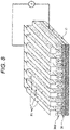
- Fig. 8 is a diagram illustrating how to form the photocatalyst electrode in Fig. 7B .
- a ferroelectric layer 30D has a plurality of periodically polarization-inverted ferroelectric domains DM1, DM2 (polarization inversion structure).
- a photocatalyst electrode 1E has the ferroelectric layer 30D placed between the electrode 20 and the semiconductor photocatalyst layer 40.
- the ferroelectric domains DM1, DM2 are arranged to have a periodic 180-degree inversion structure, so that the semiconductor photocatalyst layer 40 in contact with the top portions of the ferroelectric domains DM1, DM2 undergo periodically different electric fields (potential gradients), and the electrons and the positive holes (holes) are regularly separated according to the placement of the ferroelectric domains DM1, DM2. That is, placing the semiconductor photocatalyst layer 40 on the ferroelectric domains DM1, DM2 structured as described above enables spatial separation between the electrons and the holes and inhabitation of recombination of the electrons and the holes.
- the ferroelectric layer 30D may be formed from materials such as lithium niobate which is ferroelectrics.
- multiple stripe shaped electrodes 60 are created on the top portion of the ferroelectric layer 30D made of lithium niobate (LiNbO 3 ), then a voltage V is applied in order to make the ferroelectric domains DM1, DM2 with polarization periodically inverted by 180 degrees.
- the multiple stripe shaped electrodes 60 are removed, and the semiconductor photocatalyst layer 40 is formed to be in contact with the top portion of the ferroelectric layer 30D.
- the photocatalyst electrode 1E is formed as illustrated in Fig. 7B .
- the multiple stripe shaped electrodes 60 may not be removed, and the semiconductor photocatalyst layer 40 may be formed on the multiple stripe shaped electrodes 60 and on the top portions of the ferroelectric layer 30D exposed between the multiple stripe shaped electrodes 60, and thus forming a photocatalyst electrode.
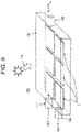
- Fig. 9 is a diagram illustrating an example conceptual configuration of a hydrogen production cell according to the embodiments.
- a hydrogen production cell 100 has a housing 101 in which an aqueous medium (H 2 O) can be stored.
- the housing 101 is provided with an inlet 102 through which the aqueous medium flows into the housing 101, an outlet 104 through which the aqueous medium flows out of the housing 101, and a gas delivery port 106 through which hydrogen and oxygen are extracted from the interior of the housing 101.
- a transparent window is installed which is formed from a transparent material such as glass and/or the like to allow the solar light 110 to pass through.
- the multiple photocatalyst electrodes 1 are installed within the housing 101. Wiring (not shown) connected to the electrodes 20 of the photocatalyst electrodes 1 is installed in the housing 101. An electric field is applied to the ferroelectric layers 30 through the wiring to control the polarization of the ferroelectric layers 30.
- the aqueous medium is introduced into the housing 101, and the multiple photocatalyst electrodes 1 are placed in the aqueous medium. While the multiple photocatalyst electrodes 1 are being placed in the aqueous medium, the multiple photocatalyst electrodes 1 are irradiated with the solar light 110, which in turn causes a water decomposition reaction by a photocatalytic reaction to occur, so that hydrogen and oxygen may be extracted through the gas delivery port 106.
- the photocatalyst electrode 1 may be replaced with the photocatalyst electrode 1A, 1B, 1C, 1D, or 1E described in the above embodiments.
- a quartz substrate 10 is prepared.
- a Pt electrode 20 is formed on the principal surface of the substrate 10.
- the electrode 20 is formed through Pt vapor deposition to a film thickness of 50 nm.
- a ferroelectric layer 30 is then formed on the electrode 20.
- the ferroelectric layer 30 is formed by performing sputtering to deposit a BaTiO 3 thin film of a thickness of 300 nm.
- a semiconductor photocatalyst layer 40 is formed on the ferroelectric layer 30.
- a target containing Y, Ti, sulfur and oxygen in a 2:2:2:5 ratio is sputtered to produce a Y 2 Ti 2 O 5 S 2 semiconductor film with a film thickness of the order of 300 nm.
- a stacking structure of the substrate 10, electrode 20, ferroelectric layer 30, and the semiconductor photocatalyst layer 40 may be formed.
- a quartz substrate 10 is prepared.
- a Pt electrode 20 is formed on the principal surface of the substrate 10.
- the electrode 20 is formed through Pt vapor deposition to a film thickness of 50 nm.
- a ferroelectric layer 30 is formed on the electrode 20.
- the ferroelectric layer 30 is formed by performing sputtering to deposit a BaTiO 3 thin film of a thickness of 10 nm. Then, a semiconductor photocatalyst layer 40 is formed on the ferroelectric layer 30.
- the semiconductor photocatalyst layer 40 for example, a target containing Y, Ti, sulfur, and oxygen in a 2:2:2:5 ratio is sputtered to produce a Y 2 Ti 2 O 5 S 2 semiconductor film with a film thickness of the order of 10 nm. Then, the BaTiO 3 thin film as a ferroelectric layer and the Y 2 Ti 2 O 5 S 2 semiconductor film as a semiconductor photocatalyst layer are produced to form a 10-period multilayer (BaTiO 3 -Y 2 Ti 2 O 5 S 2 ⁇ 10 sets) . As a result, a multiplayer stacking structure of the substrate 10, electrode 20, ferroelectric layer 30, and the semiconductor photocatalyst layer 40 may be formed.
- a quartz substrate 10 is prepared.
- a photoresist coating is applied to the principal surface of the substrate 10.
- the photoresist is patterned through photolithography to create an array structure in which 1- ⁇ m squares are arranged to be spaced at 1- ⁇ m intervals. Specifically, the photoresist is patterned such that portions where the pillar structures 70 are to be formed are removed.
- the principal surface of the substrate 10 is exposed, in the 1- ⁇ m square pattern, at the portions where the photoresist is removed.
- a Pt electrode 20 is formed on the photoresist and on the exposed area of the principal surface of the substrate 10. For example, the electrode 20 is formed through Pt vapor deposition to a film thickness of 50 nm.
- a ferroelectric layer 30 is formed on the electrode 20.
- the ferroelectric layer 30 is formed by performing sputtering to deposit a BaTiO 3 thin film of a thickness of 10 nm. Then, a semiconductor photocatalyst layer 40 is formed on the ferroelectric layer 30.
- a target containing Y, Ti, sulfur, and oxygen in a 2:2:2:5 ratio is sputtered to produce a Y 2 Ti 2 O 5 S 2 semiconductor film with a film thickness of the order of 10 nm.
- the BaTiO 3 thin film as a ferroelectric layer and the Y 2 Ti 2 O 5 S 2 semiconductor film as a semiconductor photocatalyst layer are produced to form a 10-period multilayer (BaTiO 3 -Y 2 Ti 2 O 5 S 2 ⁇ 10 sets) .
- a multiplayer stacking structure of the substrate 10, electrode 20, ferroelectric layer 30, and the semiconductor photocatalyst layer 40 may be formed.
- the photoresist is removed by performing the lift-off process.
- the pillar structures 70 may be formed.
- the 10-period multilayer staking structure of the ferroelectric layers 30 and the semiconductor photocatalyst layers 40 is unnecessary, in the process of forming the ferroelectric layer 30 on the electrode 20, sputtering is performed to deposit a BaTiO 3 thin film of a thickness of 300 nm. Then, a semiconductor photocatalyst layer 40 is formed on the ferroelectric layer 30.
- a target containing Y, Ti, sulfur and oxygen in a 2:2:2:5 ratio is sputtered to produce a Y 2 Ti 2 O 5 S 2 semiconductor film with a film thickness of the order of 300 nm. Then, the photoresist is removed by performing the lift-off process.
- a quartz substrate 10 is prepared.
- a Pt electrode 20 is formed on the principal surface of the substrate 10.
- the electrode 20 is formed through Pt vapor deposition to a film thickness of 50 nm.
- a ferroelectric layer 30D made of lithium niobate (LiNbO3) is formed on the electrode 20.
- ferroelectric domains (DM1, DM2) are formed to have polarization periodically inverted by 180 degrees (see Fig. 8 ).
- a semiconductor photocatalyst layer 40 is formed on the top portion of the ferroelectric layer 30.
- suppering is performed to produce a Y 2 Ti 2 O 5 S 2 film a film thickness of the order of 100 nm.
- a photocatalyst electrode 1E is formed.
- the photocatalyst electrode 1 produced by manufacture method 1 and illustrated in Fig. 1 is immersed in an IrO 2 colloidal dispersion solution, and then dried in a vacuum. This allows IrO 2 to adhere as promoters onto the semiconductor photocatalyst layer 40.
- the photocatalyst electrode 1 with the promoters is placed in the aqueous medium in the hydrogen production cell 100, and then irradiated with solar light. Thus, occurrence of hydrogen may be confirmed.
- Y 2 Ti 2 O 5 S 2 as a material of the semiconductor photocatalyst layer 40
- other material systems used as a base material to be doped may include, but are not limited to, ATa 2 O 6 (A:Sr,Ba), Sr 2 Nb 2 O 7 , Sr 2 Ta 2 O 7 , ATa 2 O 6 (A: Ca, Sr, Ba), K 3 Ta 3 Si 2 O 13 , ATaO 3 (A:Li,Na,K), AgTaO 3 , NaTaO 3 :La, NaTaO 3 :A(A:Ca,Sr,Ba), K 2 LnTa 5 O 15 , K 3 Ta 3 B 2 O 12 , Cs 2 Nb 4 O 11 , Ba 5 Nb 4 O 15 , ATa 3 O 8 (A:Rb,Cs), Cs 4 Ta 10 O 27 , Cs 6 Ta 16 O 43 , ZnS, NaInS 2 ,
Landscapes
- Chemical & Material Sciences (AREA)
- Organic Chemistry (AREA)
- Engineering & Computer Science (AREA)
- Chemical Kinetics & Catalysis (AREA)
- Electrochemistry (AREA)
- Materials Engineering (AREA)
- Metallurgy (AREA)
- Inorganic Chemistry (AREA)
- Health & Medical Sciences (AREA)
- General Health & Medical Sciences (AREA)
- Combustion & Propulsion (AREA)
- Catalysts (AREA)
Abstract
Photocatalyst technology is provided which is for creating a structure that facilitates spatial charge separation without individually making a p-type semiconductor and an n-type semiconductor, in order to enable separation between electrons and positive holes and inhibition of recombination. A hydrogen production cell 100 includes: a photocatalyst composed of a semiconductor; an aqueous medium; and a ferroelectric placed to face the photocatalyst, the ferroelectric creating a potential gradient with respect to the photocatalyst.
Description
- The present invention relates to a hydrogen production cell and, more particularly, to technology effectively applied to hydrogen production cells for producing hydrogen through water splitting by reaction induced by light energy.
- In recent years, various measures have taken to reduce CO2 emissions for the solution of the environmental issues such as global warming. Among them, there is a need for the promotion of utilization of zero CO2 emission power generation using renewable energy such as solar-electric power generation and wind power generation. However, because the renewable energy used in power generation is natural energy, the amount of power generation significantly varies with time of day, time of year, and geographical region. Therefore, the renewable energy is characterized by great fluctuations. For high-efficient use of such energy with great fluctuations, a system and/or functionality for adjusting energy fluctuations is absolutely essential.
- In recent years, Power to Gas (P2G) has drawn attention which is a technology to store temporarily energy such as electrical power in gaseous form. Hydrogen among gases produces only water when burning. Accordingly, the hydrogen is drawing attention as completely clean energy source without CO2 emissions. For this purpose, photocatalyst is drawing attention which enables generation of hydrogen from water and solar energy and storage of energy as hydrogen. Suggestions about such photocatalyst are described, for example, in International Publication No.
WO2017/164191 ,Japanese Unexamined Patent Application Publications Nos. 2008-104899 2017-155332 - The following technology/technique is technology/technique studied by the inventors, rather than known technology/technique.
- With the photocatalyst, the larger the band gap of a semiconductor that absorbs ultraviolet light, the higher the redox reactivity becomes, but if near-infrared and/or visible light with a large proportion of energy to solar light can be fully used, an increase in utilization efficiency of solar light may be achieved, which needs use of a suitable band gap material. Also, electron-hole pairs generated under light irradiation may be recombined prior to being used in water splitting, and therefore this creates a need for efficient separation between electrons and positive holes and inhibition of recombination.
- As a water splitting photocatalyst, a p-n junction photocatalyst with p-type and n-type semiconductors joined together has been studied. In solar cells, for the purpose of efficient separation between electrons and positive holes, a junction between the p-type semiconductor and the n-type semiconductor is made in order to create a structure that facilitates spatial separation between electrons and positive holes. Necessity for making such a p-n junction is that appropriate doping is performed to make individually the p-type semiconductor and the n-type semiconductor. However, in the case of materials for oxide semiconductor and the like, some of the materials are difficult to be made into a p-type semiconductor, and no p-type semiconductor may be obtained. The oxide semiconductor with stable structure is apt to become n-type. Because of this, it has been difficult to find out a material capable of making a p-n conjunction.
- It is an object of the present invention to create a structure that facilitates spatial charge separation without individually making a p-type semiconductor and an n-type semiconductor, in order to provide a hydrogen production cell using a photocatalyst enabling separation between electrons and positive holes and inhibition of recombination.
- These and other problems and novel features will be apparent from a reading of the following description in the specification and a review of the associated drawings.
- Typical aspects of the invention will be briefly summarized as follows.
- According to one embodiment, in a hydrogen production cell having a photocatalyst composed of a semiconductor and an aqueous medium, a ferroelectric substance is placed to face the photocatalyst, the ferroelectric substance creating a potential gradient with respect to the photocatalyst.
- According to the above embodiment, a hydrogen production cell is provided which uses a photocatalyst capable of effectively using light energy for a desired reaction such as a water decomposition reaction and/or the like.
-
-
Fig. 1 is a cross-sectional view illustrating a first example configuration of a photocatalyst electrode according to an embodiment; -
Fig. 2 is a diagram illustrating the relationship between electric field and polarization of a ferroelectric; -
Fig. 3 is a cross-sectional view illustrating a second example configuration of a photocatalyst electrode according to an embodiment; -
Fig. 4 is a cross-sectional view illustrating a third example configuration of a photocatalyst electrode according to an embodiment; -
Fig. 5 is a cross-sectional view illustrating a fourth example configuration of a photocatalyst electrode according to an embodiment; -
Fig. 6A is a plan view illustrating a fifth example configuration of a photocatalyst electrode according to an embodiment; -
Fig. 6B is a perspective view illustrating a region B inFig. 6A ; -
Fig. 6C is a cross-sectional view of the photocatalyst electrode taken along the C-C line ofFig. 6A ; -
Fig. 7A is a diagram illustrating a ferroelectric layer having a plurality of periodically polarization-inverted ferroelectric domains; -
Fig. 7B is a plan view illustrating a sixth example configuration of a photocatalyst electrode according to an embodiment; -
Fig. 8 is a diagram illustrating how to form the photocatalyst electrode inFig. 7B ; and -
Fig. 9 is a diagram illustrating an example conceptual configuration of a hydrogen production cell according to an embodiment. - Embodiments and examples according to the present invention will now be described with reference to the accompanying drawings. Throughout the description and drawings, like reference signs are used to indicate like elements and a similar description may be omitted. Although, for better understanding of the disclosure, the drawings may depict schematically as compared with practical implementations, the drawings are provided solely for illustrative purposes and should not interpreted as limiting the present invention.
- Prior to describing embodiments according to the invention, a water decomposition reaction by a photocatalytic reaction will be discussed.
- A water decomposition reaction by a photocatalytic reaction and a water electrolysis reaction caused by use of a solar cell are expressed in general by reaction a formula (1) as follows.
H2O → H2+1/2O2 (1)
- On the catalyst surface, hydrogen production and oxygen production as expressed by chemical reaction formulae (2), (3) occur individually.
2H+ + 2e- → H2 (2)
H2O → 2H+ + 2e- + 1/2O2 (3)
- When a semiconductor exhibiting photocatalytic properties absorbs light of energy greater than band gap, electrons in a valence band are excited into a conduction band, thereby producing electrons and positive holes which then initiate water splitting, respectively.
- With the photocatalyst, the larger the band gap of a semiconductor that absorbs ultraviolet light, the higher the redox reactivity becomes, but if near-infrared and/or visible light with a large proportion of energy to solar light can be fully used, an increase in utilization efficiency of solar light may be achieved, which needs use of suitable band gap materials. Also, electron-hole pairs generated under light irradiation may be recombined prior to being used in water splitting. Therefore, this creates a need for efficient separation between electrons and positive holes and inhibition of recombination.
- As described earlier, in solar cells, for the purpose of efficient separation between electrons and positive holes, a junction between a p-type semiconductor and an n-type semiconductor is made in order to create a structure that facilitates spatial separation between electrons and positive holes. Necessity for making such a p-n junction is that appropriate doping is performed to make individually the p-type semiconductor and the n-type semiconductor. However, in the case of materials for oxide semiconductors and the like, some of materials are difficult to be made into a p-type semiconductors, and thus no p-type semiconductor may be obtained.
- In the present invention, a structure by which spatial charge separation is promoted is made without individually making the p-type semiconductor and the n-type semiconductor, in order to provide separation between electrons and positive holes and inhibition of recombination thereof. Also, the surface area of a semiconductor in which the exited electrons and positive holes are utilized is increased in order to increase the reaction efficiency of water and/or a compound as fuel obtained by reduction of carbon dioxide, for use in hydrogen production. This makes it possible to provide a hydrogen production cell using a photocatalytic semiconductor which is capable of effectively using light energy for a desired reaction such as a water decomposition reaction.
- More specifically, the present invention provides a structure that enables improved efficiency of production of hydrogen and oxygen through water splitting by inhibiting recombination of carriers which are produced by irradiating, with light, a photocatalytic semiconductor of thin film or bulk. For this end, by way of example, a spontaneously polarized ferroelectric material and a semiconductor material exhibiting photocatalytic effects are stacked one on top of another. By the ferroelectric material, an effective electric field is applied to the photocatalytic semiconductor (i.e., create a potential gradient with respect to the photocatalytic semiconductor) to promote the spatial separation between electrons and positive holes and inhabit recombination of carriers. By virtue of this, the photocatalytic effects in proximity to the ferroelectric may be enhanced. This obviates the necessity of achieving separately material formations for a p-type semiconductor and an n-type semiconductor, and thus the tendency of electrons and positive holes to recombine may be reduced. Therefore, a stable hydrogen production cell is provided.
- Embodiments according to the present invention will now be described with reference to the accompanying drawings.
-
Fig. 1 is a cross-sectional view illustrating a first example configuration of a photocatalyst electrode according to the embodiments.Fig. 2 is a diagram illustrating the relationship between electric field and polarization of a ferroelectric. - As illustrated in
Fig. 1 , aphotocatalyst electrode 1 used in a hydrogen production cell has asubstrate 10, anelectrode 20 placed in contact with the top face of thesubstrate 10, aferroelectric layer 30 placed in contact with the top face of theelectrode 20, asemiconductor photocatalyst layer 40 placed in contact with the tope face of theferroelectric layer 30, andpromoters 50 adhering to the surface of thesemiconductor photocatalyst layer 40. It is to be understood that in thephotocatalyst electrode 1, thepromoters 50 are not an essential configuration, but providing thepromoters 50 may yield about an improvement in photocatalytic reaction rate. - The
substrate 10 may be formed from, for example, quartz. The electrode (also referred to as an "electrode layer") 20 may be formed from, for example, Pt (platinum). Theelectrode 20 may translate to an electrode layer. - The
ferroelectric layer 30 may be formed by use of, for example, BaTiO3, Pb(Zr,Ti)O3, LiNbO3, LiTaO3, YbFe2O4 and/or the like. For theferroelectric layer 30, multiferroic materials with magnetization at room temperature such as Pb3TeMn3P2O14 may be used. The use of the multiferroic materials enables control on the direction of electric polarization by magnetic fields. - The
semiconductor photocatalyst layer 40 may be formed by use of a material selected from the group of, for example, ATa2O6 (A: Sr, Ba), Sr2Nb2O7, Sr2Ta2O7, ATa2O6 (A: Ca, Sr, Ba), K3Ta3Si2O13, ATaO3 (A:Li,Na,K), AgTaO3, NaTaO3, K2LnTa5O15, K3Ta3B2O12, Cs2Nb4O11, Ba5Nb4O15, ATa3O8 (A:Rb, Cs), Cs4Ta10O27, Cs6Ta16O43, ZnS, NaInS2, SrTiO3, AgGaS2, CuGaS2, CuInS2-AgInS2-ZnS, CuInS2-AgInS2, A2Ti2O7 (A: Sc, Y, La), SnNb2O6, BiVO4, Bi2MoO6, Bi2WO6, AgNbO3, Ag3VO4, Ag0.5Pr0.5TiO3, TiO2, PbMoO4:Cr, SrTiO3:Ir, SnNb2O6 and the like. A material resulting from substitution of nitrogen or sulfur for a portion of oxygen in the above materials may be used for thesemiconductor photocatalyst layer 40. The materials mentioned above are illustrative only, and any semiconductor material other than the above may be used for thesemiconductor photocatalyst layer 40. - The
promoters 50 include Pt (platinum), Ru (ruthenium), Rh (rhodium), Cr (chromium), and/or the like. - As illustrated in
Fig. 1 , theferroelectric layer 30 and thesemiconductor photocatalyst layer 40 are stacked one on top of another. Because of this, theferroelectric layer 30 is placed to face thesemiconductor photocatalyst layer 40. An electric field is applied from theelectrode 20 to theferroelectric layer 30, so that theferroelectric layer 30 may change the direction of polarization. As illustrated inFig. 1 , theferroelectric layer 30 is designed such thatelectric polarization 35 is in a direction perpendicular to the top face of the substrate 10 (in the upward direction in the example). Typically, the relationship between the ferroelectricelectric polarization 35 and an electric field exhibits hysteresis characteristics as illustrated inFig. 2 . When an electric field is applied to orient the polarization to the same direction, the state ofspontaneous polarization 35 is maintained. By using such materials, an electric field is applied to thesemiconductor photocatalyst layer 40 located close to theferroelectric layer 30. By theferroelectric layer 30, an effective electric field is applied to thesemiconductor photocatalyst layer 40, that is, a potential gradient is created with respect to thesemiconductor photocatalyst layer 40 to promote the spatial separation between electrons and positive holes and inhabit recombination of carriers. By virtue of this, the photocatalytic effects may be enhanced in thesemiconductor photocatalyst layer 40 in proximity to theferroelectric layer 30. - The
photocatalyst electrode 1 is immersed in an aqueous medium stored in the hydrogen production cell, and thephotocatalyst electrode 1 is irradiated with, for example, solar light. The light irradiation allows thesemiconductor photocatalyst layer 40 to produce carriers (electrons and positive holes). Here, theferroelectric layer 30 is electrically polarized, and an electric field (potential gradient) is applied to thesemiconductor photocatalyst layer 40 by the electric polarization. As a result, spatial charge separation between the electrons and positive holes generated by the light irradiation is induced in thesemiconductor photocatalyst layer 40, and recombination of the electrons and the positive holes is inhibited. The electron and the positive holes after the spatial charge separation within thesemiconductor photocatalyst layer 40 initiate a decomposition reaction of the aqueous medium with high efficiency, and thus hydrogen and oxygen are generated. -
Fig. 3 is a cross-sectional view illustrating a second example configuration of a photocatalyst electrode according to the embodiments. The difference between aphotocatalyst electrode 1A illustrated inFig. 3 and thephotocatalyst electrode 1 inFig. 1 is that, in thephotocatalyst electrode 1A, aferroelectric layer 30A, asemiconductor photocatalyst layer 40A, aferroelectric layer 30B, and asemiconductor photocatalyst layer 40B are stacked in this order on asemiconductor photocatalyst layer 40 in a multilayer fashion. By stacking the ferroelectric layers (30, 30A, 30B) and the semiconductor photocatalyst layers (40, 40A, 40B) in a multilayer fashion, the number of interfaces between the semiconductor photocatalyst layer (40, 40A, 40B) and the ferroelectric layer (30, 30A, 30B) may be increased. Because of charge bias arising in proximity to the interface between the semiconductor photocatalyst layer and the ferroelectric layer, one of both the electrons and the positive holes is collected according to the direction of thepolarization 35 of the ferroelectric layer (30, 30A, 30B). Therefore, the charges are particularly spatially separated in proximity to the interface. Thus, the number of electrons or positive holes in thephotocatalyst electrode 1A inFig. 3 may be increased as compared with that in thephotocatalyst electrode 1 inFig. 1 . - In this manner, a plurality of sets of the ferroelectric layer (30, 30A, 30B) and the semiconductor photocatalyst layer (40, 40A, 40B) are provided, so that it is possible to increase the surface area (the interface area) of the semiconductor photocatalyst layer (40, 40A, 40B) in which the electrons and positive holes excited by the light irradiation are used. This enables an increase in reaction efficiency of a compound used in hydrogen production.
-
Fig. 4 is a cross-sectional view illustrating a third example configuration of a photocatalyst electrode according to the embodiments. The difference between aphotocatalyst electrode 1B illustrated inFig. 4 and thephotocatalyst electrode 1 inFig. 1 is that, in thephotocatalyst electrode 1B, theelectrode 20, theferroelectric layer 30, and thesemiconductor catalyst layer 40 are designed as apillar structure 70, and a plurality ofpillar structures 70 are formed on the top face (surface) of thesubstrate 10. Thepromotors 50 may be placed on the top faces of thesemiconductor catalyst layer 40.Fig. 4 illustrates sixpillar structures 70 by way of example, but the number ofpillar structures 70 is not limited to this. By arranging thepillar structures 70, the contact area of thesemiconductor photocatalyst layer 40 with a solvent such as an aqueous medium and the like (the area of the side faces of the photocatalyst layer 40) may be increased by the number ofpillar structures 70. This may increase the frequency of occurrence of reactions used for the hydrogen production. -
Fig. 5 is a cross-sectional view illustrating a fourth example configuration of a photocatalyst electrode according to the embodiments. The differences between aphotocatalyst electrode 1C illustrated inFig. 5 and thephotocatalyst electrode 1 inFig. 1 are, in thephotocatalyst electrode 1C, that aferroelectric layer 30C is formed in contact with the top face (surface) of thesubstrate 10 and that theferroelectric layer 30C is formed between a first electrode (electrode layer) 20A and a second electrode (electrode layer) 20B.Electric polarization 36 of theferroelectric layer 30C is oriented in a direction parallel to the top face of the substrate 10 (horizontal direction) in accordance with the direction of the electric field applied by theelectrode 20A and theelectrode 20B. In this manner, theferroelectric layer 30C and theelectrodes substrate 10. The structure of sandwiching theferroelectric layer 30C between theelectrodes ferroelectric layer 30C through theelectrodes ferroelectric layer 30C is controlled. - The two
electrodes Fig. 5 may be, in planar view, two comb electrodes, first electrode 20CA and a second electrode 20CB, as illustrated inFig. 6A. Fig. 6A is a plan view illustrating a fifth example configuration of a photocatalyst electrode according to the embodiments.Fig. 6B is a perspective view illustrating a region B inFig. 6A .Fig. 6C is a cross-sectional view of the photocatalyst electrode taken along the C-C line ofFig. 6A . In aphotocatalyst electrode 1D illustrated inFig. 6A to Fig. 6C , an electric field may be applied to ferroelectric layers 30C1, 30C2 by the two comb electrodes, the first electrode 20CA and the second electrode 20CB. This enables the control of the polarization directions of the ferroelectric layers 30C1, 30C2 as illustrated inFig. 6C . In an example illustrated inFig. 6C , the direction of thepolarization 35B of the ferroelectric layer 30C2 is 180 degrees different from the direction of thepolarization 35A of the ferroelectric layer 30C1. In this manner, it is possible to make the ferroelectric layers 30C1, 30C2 respectively having the same polarization directions. - In the configuration of the
photocatalyst electrode 1D inFig. 6A to Fig. 6C , the ferroelectric layers (30C2 or 30C1) with the polarization direction oriented to the same direction may be designed by removing both of the ferroelectric layers 30C1 and the semiconductor layers 40 formed on the ferroelectric layers 30C1 or by removing both of the ferroelectric layers 30C2 and the semiconductor layers 40 formed on the ferroelectric layers 30C2. Thepromotors 50 may be placed on the top faces of the semiconductor catalyst layers 40. - The
ferroelectric layer 30 inFig. 1 may be designed to have a plurality of periodically polarization-inverted ferroelectric domains.Fig. 7A is a diagram illustrating a ferroelectric layer having a plurality of periodically polarization-inverted ferroelectric domains.Fig. 7B is a plan view illustrating a sixth example configuration of a photocatalyst electrode according to the embodiments.Fig. 8 is a diagram illustrating how to form the photocatalyst electrode inFig. 7B . - As illustrated in
Fig. 7A , aferroelectric layer 30D has a plurality of periodically polarization-inverted ferroelectric domains DM1, DM2 (polarization inversion structure). As illustrated inFig. 7B , aphotocatalyst electrode 1E has theferroelectric layer 30D placed between theelectrode 20 and thesemiconductor photocatalyst layer 40. In this manner, the ferroelectric domains DM1, DM2 are arranged to have a periodic 180-degree inversion structure, so that thesemiconductor photocatalyst layer 40 in contact with the top portions of the ferroelectric domains DM1, DM2 undergo periodically different electric fields (potential gradients), and the electrons and the positive holes (holes) are regularly separated according to the placement of the ferroelectric domains DM1, DM2. That is, placing thesemiconductor photocatalyst layer 40 on the ferroelectric domains DM1, DM2 structured as described above enables spatial separation between the electrons and the holes and inhabitation of recombination of the electrons and the holes. Theferroelectric layer 30D may be formed from materials such as lithium niobate which is ferroelectrics. - As illustrated in
Fig. 8 , multiple stripe shapedelectrodes 60 are created on the top portion of theferroelectric layer 30D made of lithium niobate (LiNbO3), then a voltage V is applied in order to make the ferroelectric domains DM1, DM2 with polarization periodically inverted by 180 degrees. After that, the multiple stripe shapedelectrodes 60 are removed, and thesemiconductor photocatalyst layer 40 is formed to be in contact with the top portion of theferroelectric layer 30D. As a result, thephotocatalyst electrode 1E is formed as illustrated inFig. 7B . Although not shown, the multiple stripe shapedelectrodes 60 may not be removed, and thesemiconductor photocatalyst layer 40 may be formed on the multiple stripe shapedelectrodes 60 and on the top portions of theferroelectric layer 30D exposed between the multiple stripe shapedelectrodes 60, and thus forming a photocatalyst electrode. -
Fig. 9 is a diagram illustrating an example conceptual configuration of a hydrogen production cell according to the embodiments. As illustrated inFig. 9 , ahydrogen production cell 100 has ahousing 101 in which an aqueous medium (H2O) can be stored. Thehousing 101 is provided with aninlet 102 through which the aqueous medium flows into thehousing 101, anoutlet 104 through which the aqueous medium flows out of thehousing 101, and agas delivery port 106 through which hydrogen and oxygen are extracted from the interior of thehousing 101. In a portion of thehousing 101, a transparent window is installed which is formed from a transparent material such as glass and/or the like to allow thesolar light 110 to pass through. Themultiple photocatalyst electrodes 1 are installed within thehousing 101. Wiring (not shown) connected to theelectrodes 20 of thephotocatalyst electrodes 1 is installed in thehousing 101. An electric field is applied to theferroelectric layers 30 through the wiring to control the polarization of the ferroelectric layers 30. - The aqueous medium is introduced into the
housing 101, and themultiple photocatalyst electrodes 1 are placed in the aqueous medium. While themultiple photocatalyst electrodes 1 are being placed in the aqueous medium, themultiple photocatalyst electrodes 1 are irradiated with thesolar light 110, which in turn causes a water decomposition reaction by a photocatalytic reaction to occur, so that hydrogen and oxygen may be extracted through thegas delivery port 106. In this regard, thephotocatalyst electrode 1 may be replaced with thephotocatalyst electrode - Next, an example method of manufacturing a photocatalyst electrode will be described.
- A
quartz substrate 10 is prepared. APt electrode 20 is formed on the principal surface of thesubstrate 10. For example, theelectrode 20 is formed through Pt vapor deposition to a film thickness of 50 nm. Aferroelectric layer 30 is then formed on theelectrode 20. For example, theferroelectric layer 30 is formed by performing sputtering to deposit a BaTiO3 thin film of a thickness of 300 nm. Then, asemiconductor photocatalyst layer 40 is formed on theferroelectric layer 30. For thesemiconductor photocatalyst layer 40, for example, a target containing Y, Ti, sulfur and oxygen in a 2:2:2:5 ratio is sputtered to produce a Y2Ti2O5S2 semiconductor film with a film thickness of the order of 300 nm. As a result, a stacking structure of thesubstrate 10,electrode 20,ferroelectric layer 30, and thesemiconductor photocatalyst layer 40 may be formed. - A
quartz substrate 10 is prepared. APt electrode 20 is formed on the principal surface of thesubstrate 10. For example, theelectrode 20 is formed through Pt vapor deposition to a film thickness of 50 nm. Aferroelectric layer 30 is formed on theelectrode 20. For example, theferroelectric layer 30 is formed by performing sputtering to deposit a BaTiO3 thin film of a thickness of 10 nm. Then, asemiconductor photocatalyst layer 40 is formed on theferroelectric layer 30. For thesemiconductor photocatalyst layer 40, for example, a target containing Y, Ti, sulfur, and oxygen in a 2:2:2:5 ratio is sputtered to produce a Y2Ti2O5S2 semiconductor film with a film thickness of the order of 10 nm. Then, the BaTiO3 thin film as a ferroelectric layer and the Y2Ti2O5S2 semiconductor film as a semiconductor photocatalyst layer are produced to form a 10-period multilayer (BaTiO3-Y2Ti2O5S2 × 10 sets) . As a result, a multiplayer stacking structure of thesubstrate 10,electrode 20,ferroelectric layer 30, and thesemiconductor photocatalyst layer 40 may be formed. - A
quartz substrate 10 is prepared. A photoresist coating is applied to the principal surface of thesubstrate 10. The photoresist is patterned through photolithography to create an array structure in which 1-µm squares are arranged to be spaced at 1-µm intervals. Specifically, the photoresist is patterned such that portions where thepillar structures 70 are to be formed are removed. The principal surface of thesubstrate 10 is exposed, in the 1-µm square pattern, at the portions where the photoresist is removed. Then, aPt electrode 20 is formed on the photoresist and on the exposed area of the principal surface of thesubstrate 10. For example, theelectrode 20 is formed through Pt vapor deposition to a film thickness of 50 nm. Aferroelectric layer 30 is formed on theelectrode 20. For example, theferroelectric layer 30 is formed by performing sputtering to deposit a BaTiO3 thin film of a thickness of 10 nm. Then, asemiconductor photocatalyst layer 40 is formed on theferroelectric layer 30. For thesemiconductor photocatalyst layer 40, for example, a target containing Y, Ti, sulfur, and oxygen in a 2:2:2:5 ratio is sputtered to produce a Y2Ti2O5S2 semiconductor film with a film thickness of the order of 10 nm. Then, the BaTiO3 thin film as a ferroelectric layer and the Y2Ti2O5S2 semiconductor film as a semiconductor photocatalyst layer are produced to form a 10-period multilayer (BaTiO3-Y2Ti2O5S2 × 10 sets) . As a result, a multiplayer stacking structure of thesubstrate 10,electrode 20,ferroelectric layer 30, and thesemiconductor photocatalyst layer 40 may be formed. Then, the photoresist is removed by performing the lift-off process. As a result, thepillar structures 70 may be formed. - If the 10-period multilayer staking structure of the
ferroelectric layers 30 and the semiconductor photocatalyst layers 40 is unnecessary, in the process of forming theferroelectric layer 30 on theelectrode 20, sputtering is performed to deposit a BaTiO3 thin film of a thickness of 300 nm. Then, asemiconductor photocatalyst layer 40 is formed on theferroelectric layer 30. For thesemiconductor photocatalyst layer 40, for example, a target containing Y, Ti, sulfur and oxygen in a 2:2:2:5 ratio is sputtered to produce a Y2Ti2O5S2 semiconductor film with a film thickness of the order of 300 nm. Then, the photoresist is removed by performing the lift-off process. - A
quartz substrate 10 is prepared. APt electrode 20 is formed on the principal surface of thesubstrate 10. For example, theelectrode 20 is formed through Pt vapor deposition to a film thickness of 50 nm. Aferroelectric layer 30D made of lithium niobate (LiNbO3) is formed on theelectrode 20. In theferroelectric layer 30D, ferroelectric domains (DM1, DM2) are formed to have polarization periodically inverted by 180 degrees (seeFig. 8 ). Asemiconductor photocatalyst layer 40 is formed on the top portion of theferroelectric layer 30. For thesemiconductor photocatalyst layer 40, for example, suppering is performed to produce a Y2Ti2O5S2 film a film thickness of the order of 100 nm. As a result, aphotocatalyst electrode 1E is formed. - The
photocatalyst electrode 1 produced bymanufacture method 1 and illustrated inFig. 1 is immersed in an IrO2 colloidal dispersion solution, and then dried in a vacuum. This allows IrO2 to adhere as promoters onto thesemiconductor photocatalyst layer 40. Thephotocatalyst electrode 1 with the promoters is placed in the aqueous medium in thehydrogen production cell 100, and then irradiated with solar light. Thus, occurrence of hydrogen may be confirmed. - In the above description of the manufacture methods, the instance of using Y2Ti2O5S2 as a material of the
semiconductor photocatalyst layer 40 has been mentioned, but other material systems used as a base material to be doped may include, but are not limited to, ATa2O6(A:Sr,Ba), Sr2Nb2O7, Sr2Ta2O7, ATa2O6 (A: Ca, Sr, Ba), K3Ta3Si2O13, ATaO3 (A:Li,Na,K), AgTaO3, NaTaO3:La, NaTaO3:A(A:Ca,Sr,Ba), K2LnTa5O15, K3Ta3B2O12, Cs2Nb4O11, Ba5Nb4O15, ATa3O8 (A:Rb,Cs), Cs4Ta10O27, Cs6Ta16O43, ZnS, NaInS2, SrTiO3, AgGaS2, CuGaS2, CuInS2-AgInS2-ZnS, CuInS2-AgInS2, SnNb2O6, BiVO4, Bi2MoO6, Bi2WO6, AgNbO3, Ag3VO4, Ag0.5Pr0.5TiO3, TiO2, PbMoO4:Cr, A2Ti2O7 (A:Sc,Y,La), SnNb2O6, and the like. Likewise in regard to theferroelectric layer 30, not only BaTiO3 but also other spontaneously polarizing materials may be used. - The present invention carried out by the inventors has been detailed based on example embodiments, but it will be apparent that the present invention is not limited to the above embodiments and various modifications and variations can be made to the embodiments.
-
- 1, 1A, 1B, 1C, 1D, 1E ... photocatalyst electrode
- 10 ... substrate
- 20, 20A, 20B, 20CA, 20CB ... electrode
- 30, 30A, 30B, 30C, 30C1, 30C2, 30D ... ferroelectric layer
- 35 ... polarization
- 40 ... semiconductor photocatalyst layer
- 50 ... promoter
- 60 ... stripe shaped electrode
- 70 ... pillar structure
- 100 ... hydrogen production cell
- 101 ... housing
- 102 ... inlet
- 104 ... outlet
- 106 ... gas delivery port
- 110 ... solar light
Claims (13)
- A hydrogen production cell comprising:a photocatalyst composed of a semiconductor;an aqueous medium; anda ferroelectric substance placed to face the photocatalyst, the ferroelectric creating a potential gradient with respect to the photocatalyst.
- The hydrogen production cell according to claim 1 comprising a plurality of sets of the photocatalyst and the ferroelectric substance.
- The hydrogen production cell according to claim 1, wherein the ferroelectric substance is a multiferroic substance exhibiting magnetization at room temperature.
- The hydrogen production cell according to claim 1, wherein the ferroelectric substance has periodically polarization-inverted ferroelectric domains (DM1, DM2), the ferroelectric domains (DM1, DM2) presenting respective potential gradients in different directions.
- The hydrogen production cell according to claim 1, wherein the ferroelectric substance and the photocatalyst have a pillar structure (70).
- The hydrogen production cell according to claim 1,a housing (10) in which the aqueous medium is stored; anda photocatalyst electrode placed in the aqueous medium,wherein the photocatalyst electrode includesthe photocatalyst layer composed of a semiconductor, andthe ferroelectric layer (30) creating a potential gradient with respect to the photocatalyst layer, andthe ferroelectric layer (30) is placed to face the photocatalyst layer.
- The hydrogen production cell according to claim 6 (30), wherein the photocatalyst layer and the ferroelectric layer are designed as a multilayer structure having a plurality of sets of the photocatalyst layer and the ferroelectric layer (30, 30A, 30B, 30C, 30C1, 30C2, 30D).
- The hydrogen production cell according to claim 6, wherein the photocatalyst electrode includesa substrate (10),a plurality of the ferroelectric layers (30) that are placed on the substrate (10), anda plurality of the photocatalyst layers that are respectively placed in contact with tops of the plurality of the ferroelectric layers (30), andeach of the ferroelectric layers (30) and each of the photocatalyst layers that is placed in contact with the top of the corresponding ferroelectric layer (30) are designed as a pillar structure (70).
- The hydrogen production cell according to claim 6,wherein the ferroelectric layer (30) has a plurality of periodically polarization-inverted ferroelectric domains (DM1, DM2), andthe photoelectric layer (30) is subjected to periodically different potential gradients by the plurality of the ferroelectric domains (DM1, DM2).
- The hydrogen production cell according to claim 6, wherein the photocatalyst electrode (1, 1A, 1B, 1C, 1D, 1E) includesa substrate (10), andan electric layer (30) formed on the substrate (10), andthe ferroelectric layer is formed in contact with a top of the electrode layer.
- The hydrogen production cell according to claim 6, wherein the photocatalyst electrode includesa substrate (10), anda first electrode layer and a second electrode layer that are formed on the substrate (10),the ferroelectric layer (30) is formed on the substrate (10) and between the first electrode layer and the second electrode layer, and
the ferroelectric layer (30) is given an electric field by the first electrode layer and the second electrode layer. - The hydrogen production cell according to claim 11, wherein the first electrode layer forms a comb electrode in planar view, and the second electrode layer forms a comb electrode in planar view.
- The hydrogen production cell according to claim 6, wherein the ferroelectric layer (30) is formed from multiferroic materials exhibiting magnetization at room temperature.
Applications Claiming Priority (1)
| Application Number | Priority Date | Filing Date | Title |
|---|---|---|---|
| JP2021094971A JP2022187124A (en) | 2021-06-07 | 2021-06-07 | hydrogen generation cell |
Publications (1)
| Publication Number | Publication Date |
|---|---|
| EP4101811A1 true EP4101811A1 (en) | 2022-12-14 |
Family
ID=80624965
Family Applications (1)
| Application Number | Title | Priority Date | Filing Date |
|---|---|---|---|
| EP22159853.5A Pending EP4101811A1 (en) | 2021-06-07 | 2022-03-03 | Hydrogen production cell |
Country Status (2)
| Country | Link |
|---|---|
| EP (1) | EP4101811A1 (en) |
| JP (1) | JP2022187124A (en) |
Citations (10)
| Publication number | Priority date | Publication date | Assignee | Title |
|---|---|---|---|---|
| JP2008104899A (en) | 2006-10-23 | 2008-05-08 | Sharp Corp | Photocatalyst film, method for producing photocatalyst film, and hydrogen generator using the same |
| US20170191172A1 (en) * | 2014-09-29 | 2017-07-06 | Fujifilm Corporation | Artificial photosynthesis module |
| JP2017155332A (en) | 2016-03-01 | 2017-09-07 | パナソニックIpマネジメント株式会社 | Photoelectrode and method for producing the same, and photoelectrochemical cell |
| WO2017164191A1 (en) | 2016-03-22 | 2017-09-28 | イムラ・ジャパン株式会社 | Photoelectrode, photoelectrochemical system for water decomposition, and method for producing photoelectrode |
| US10047444B2 (en) * | 2013-04-26 | 2018-08-14 | Panasonic Intellectual Property Management Co., Ltd. | Method for generating hydrogen and hydrogen generation device used therefor |
| US20190017180A1 (en) * | 2016-01-04 | 2019-01-17 | Total Raffinage Chime | Photocathode for a photoelectrolysis device, method for producing such a photocathode, and photoelectrolysis device |
| CN110600560A (en) * | 2019-07-30 | 2019-12-20 | 纳晶科技股份有限公司 | Quantum dot heterojunction and application thereof |
| CN110656350A (en) * | 2019-11-13 | 2020-01-07 | 苏州大学 | Ferroelectric thin film ternary composite photoelectrode and preparation method thereof |
| US20200385873A1 (en) * | 2018-03-06 | 2020-12-10 | Fujifilm Corporation | Photocatalytic electrode for water splitting and water splitting device |
| US20210115575A1 (en) * | 2019-10-04 | 2021-04-22 | Research & Business Foundation Sungkyunkwan University | Hydrogen evolution apparatus |
-
2021
- 2021-06-07 JP JP2021094971A patent/JP2022187124A/en active Pending
-
2022
- 2022-03-03 EP EP22159853.5A patent/EP4101811A1/en active Pending
Patent Citations (10)
| Publication number | Priority date | Publication date | Assignee | Title |
|---|---|---|---|---|
| JP2008104899A (en) | 2006-10-23 | 2008-05-08 | Sharp Corp | Photocatalyst film, method for producing photocatalyst film, and hydrogen generator using the same |
| US10047444B2 (en) * | 2013-04-26 | 2018-08-14 | Panasonic Intellectual Property Management Co., Ltd. | Method for generating hydrogen and hydrogen generation device used therefor |
| US20170191172A1 (en) * | 2014-09-29 | 2017-07-06 | Fujifilm Corporation | Artificial photosynthesis module |
| US20190017180A1 (en) * | 2016-01-04 | 2019-01-17 | Total Raffinage Chime | Photocathode for a photoelectrolysis device, method for producing such a photocathode, and photoelectrolysis device |
| JP2017155332A (en) | 2016-03-01 | 2017-09-07 | パナソニックIpマネジメント株式会社 | Photoelectrode and method for producing the same, and photoelectrochemical cell |
| WO2017164191A1 (en) | 2016-03-22 | 2017-09-28 | イムラ・ジャパン株式会社 | Photoelectrode, photoelectrochemical system for water decomposition, and method for producing photoelectrode |
| US20200385873A1 (en) * | 2018-03-06 | 2020-12-10 | Fujifilm Corporation | Photocatalytic electrode for water splitting and water splitting device |
| CN110600560A (en) * | 2019-07-30 | 2019-12-20 | 纳晶科技股份有限公司 | Quantum dot heterojunction and application thereof |
| US20210115575A1 (en) * | 2019-10-04 | 2021-04-22 | Research & Business Foundation Sungkyunkwan University | Hydrogen evolution apparatus |
| CN110656350A (en) * | 2019-11-13 | 2020-01-07 | 苏州大学 | Ferroelectric thin film ternary composite photoelectrode and preparation method thereof |
Non-Patent Citations (1)
| Title |
|---|
| YANG WEIGUANG ET AL: "Ferroelectric Polarization-Enhanced Photoelectrochemical Water Splitting in TiO 2 -BaTiO 3 Core-Shell Nanowire Photoanodes", NANO LETTERS, vol. 15, no. 11, 11 November 2015 (2015-11-11), US, pages 7574 - 7580, XP055946518, ISSN: 1530-6984, DOI: 10.1021/acs.nanolett.5b03988 * |
Also Published As
| Publication number | Publication date |
|---|---|
| JP2022187124A (en) | 2022-12-19 |
Similar Documents
| Publication | Publication Date | Title |
|---|---|---|
| Yang et al. | Manipulation of oxygen vacancy for high photovoltaic output in bismuth ferrite films | |
| Assavachin et al. | Ferroelectric polarization in BaTiO3 nanocrystals controls photoelectrochemical water oxidation and photocatalytic hydrogen evolution | |
| Zhang et al. | Facet-oriented assembly of Mo: BiVO4 and Rh: SrTiO3 particles: integration of p–n conjugated photo-electrochemical system in a particle applied to photocatalytic overall water splitting | |
| Maeda | Rhodium-doped barium titanate perovskite as a stable p-type semiconductor photocatalyst for hydrogen evolution under visible light | |
| Seger et al. | 2-Photon tandem device for water splitting: comparing photocathode first versus photoanode first designs | |
| Biswas et al. | Ultrafast electron trapping and defect-mediated recombination in NiO probed by femtosecond extreme ultraviolet reflection–absorption spectroscopy | |
| Sum et al. | Advancements in perovskite solar cells: photophysics behind the photovoltaics | |
| Yang et al. | Ferroelectric polarization-enhanced photoelectrochemical water splitting in TiO2–BaTiO3 core–shell nanowire photoanodes | |
| An et al. | Scalable photoelectrochemical cell for overall solar water splitting into H2 and H2O2 | |
| Reijnen et al. | Comparison of Cu x S films grown by atomic layer deposition and chemical vapor deposition | |
| Kawase et al. | Maximizing Oxygen Evolution Performance on a Transparent NiFeO x/Ta3N5 Photoelectrode Fabricated on an Insulator | |
| Sun et al. | Electrochromic properties of perovskite NdNiO3 thin films for smart windows | |
| Li et al. | Photovoltaic effect induced by self-polarization in BiFeO3 films | |
| Fan | Newly emerging borate-based nonlinear optical materials for organic pollutant degradation: A review | |
| Ganesh et al. | Built-in electric field for efficient charge separation and ionic transport in LiCoO2/SnO2 semiconductor junction fuel cells | |
| Wang et al. | Photocathodic behavior of ferroelectric Pb (Zr, Ti) O 3 films decorated with silver nanoparticles | |
| Kim et al. | Tailoring of interfacial band offsets by an atomically thin polar insulating layer to enhance the water-splitting performance of oxide heterojunction photoanodes | |
| Magnan et al. | Tuning the charge carriers migration in epitaxial BaTiO3 thin-film photoanodes | |
| Xiang et al. | Mapping Quantum Yield for (Fe–Zn–Sn–Ti) O x Photoabsorbers Using a High Throughput Photoelectrochemical Screening System | |
| Chang et al. | Tuning photovoltaic performance of perovskite nickelates heterostructures by changing the A-site rare-earth element | |
| Gunawan et al. | Ferroelectric materials as photoelectrocatalysts: photoelectrode design rationale and strategies | |
| Jia et al. | “Electricity”‐Assisted Catalytic Solar‐to‐Fuel Processes | |
| Gou et al. | Anion ordered and ferroelectric Ruddlesden–Popper oxynitride Ca3Nb2N2O5 for visible-light-active photocatalysis | |
| Singh et al. | Photoelectrochemically induced CO2 reduction using halide-tunable lead-free perovskites | |
| Li et al. | Synthesis and SPEF-induced enhanced photoelectrochemical performance of the BaTiO3@ α-Fe2O3 ferroelectric heterojunction |
Legal Events
| Date | Code | Title | Description |
|---|---|---|---|
| PUAI | Public reference made under article 153(3) epc to a published international application that has entered the european phase |
Free format text: ORIGINAL CODE: 0009012 |
|
| STAA | Information on the status of an ep patent application or granted ep patent |
Free format text: STATUS: REQUEST FOR EXAMINATION WAS MADE |
|
| 17P | Request for examination filed |
Effective date: 20220318 |
|
| AK | Designated contracting states |
Kind code of ref document: A1 Designated state(s): AL AT BE BG CH CY CZ DE DK EE ES FI FR GB GR HR HU IE IS IT LI LT LU LV MC MK MT NL NO PL PT RO RS SE SI SK SM TR |
|
| STAA | Information on the status of an ep patent application or granted ep patent |
Free format text: STATUS: EXAMINATION IS IN PROGRESS |
|
| 17Q | First examination report despatched |
Effective date: 20250805 |