EP4099491A2 - Battery assembly and electronic atomizing device - Google Patents
Battery assembly and electronic atomizing device Download PDFInfo
- Publication number
- EP4099491A2 EP4099491A2 EP22176446.7A EP22176446A EP4099491A2 EP 4099491 A2 EP4099491 A2 EP 4099491A2 EP 22176446 A EP22176446 A EP 22176446A EP 4099491 A2 EP4099491 A2 EP 4099491A2
- Authority
- EP
- European Patent Office
- Prior art keywords
- clamping
- component
- clamping piece
- battery assembly
- circuit board
- Prior art date
- Legal status (The legal status is an assumption and is not a legal conclusion. Google has not performed a legal analysis and makes no representation as to the accuracy of the status listed.)
- Pending
Links
Images

Classifications
-
- A—HUMAN NECESSITIES
- A24—TOBACCO; CIGARS; CIGARETTES; SIMULATED SMOKING DEVICES; SMOKERS' REQUISITES
- A24F—SMOKERS' REQUISITES; MATCH BOXES; SIMULATED SMOKING DEVICES
- A24F40/00—Electrically operated smoking devices; Component parts thereof; Manufacture thereof; Maintenance or testing thereof; Charging means specially adapted therefor
- A24F40/40—Constructional details, e.g. connection of cartridges and battery parts
-
- A—HUMAN NECESSITIES
- A24—TOBACCO; CIGARS; CIGARETTES; SIMULATED SMOKING DEVICES; SMOKERS' REQUISITES
- A24F—SMOKERS' REQUISITES; MATCH BOXES; SIMULATED SMOKING DEVICES
- A24F40/00—Electrically operated smoking devices; Component parts thereof; Manufacture thereof; Maintenance or testing thereof; Charging means specially adapted therefor
- A24F40/40—Constructional details, e.g. connection of cartridges and battery parts
- A24F40/46—Shape or structure of electric heating means
-
- H—ELECTRICITY
- H01—ELECTRIC ELEMENTS
- H01M—PROCESSES OR MEANS, e.g. BATTERIES, FOR THE DIRECT CONVERSION OF CHEMICAL ENERGY INTO ELECTRICAL ENERGY
- H01M10/00—Secondary cells; Manufacture thereof
- H01M10/42—Methods or arrangements for servicing or maintenance of secondary cells or secondary half-cells
- H01M10/425—Structural combination with electronic components, e.g. electronic circuits integrated to the outside of the casing
-
- H—ELECTRICITY
- H01—ELECTRIC ELEMENTS
- H01M—PROCESSES OR MEANS, e.g. BATTERIES, FOR THE DIRECT CONVERSION OF CHEMICAL ENERGY INTO ELECTRICAL ENERGY
- H01M10/00—Secondary cells; Manufacture thereof
- H01M10/42—Methods or arrangements for servicing or maintenance of secondary cells or secondary half-cells
- H01M10/425—Structural combination with electronic components, e.g. electronic circuits integrated to the outside of the casing
- H01M10/4257—Smart batteries, e.g. electronic circuits inside the housing of the cells or batteries
-
- H—ELECTRICITY
- H01—ELECTRIC ELEMENTS
- H01M—PROCESSES OR MEANS, e.g. BATTERIES, FOR THE DIRECT CONVERSION OF CHEMICAL ENERGY INTO ELECTRICAL ENERGY
- H01M50/00—Constructional details or processes of manufacture of the non-active parts of electrochemical cells other than fuel cells, e.g. hybrid cells
- H01M50/20—Mountings; Secondary casings or frames; Racks, modules or packs; Suspension devices; Shock absorbers; Transport or carrying devices; Holders
- H01M50/202—Casings or frames around the primary casing of a single cell or a single battery
-
- H—ELECTRICITY
- H01—ELECTRIC ELEMENTS
- H01M—PROCESSES OR MEANS, e.g. BATTERIES, FOR THE DIRECT CONVERSION OF CHEMICAL ENERGY INTO ELECTRICAL ENERGY
- H01M50/00—Constructional details or processes of manufacture of the non-active parts of electrochemical cells other than fuel cells, e.g. hybrid cells
- H01M50/20—Mountings; Secondary casings or frames; Racks, modules or packs; Suspension devices; Shock absorbers; Transport or carrying devices; Holders
- H01M50/204—Racks, modules or packs for multiple batteries or multiple cells
- H01M50/207—Racks, modules or packs for multiple batteries or multiple cells characterised by their shape
- H01M50/213—Racks, modules or packs for multiple batteries or multiple cells characterised by their shape adapted for cells having curved cross-section, e.g. round or elliptic
-
- H—ELECTRICITY
- H01—ELECTRIC ELEMENTS
- H01M—PROCESSES OR MEANS, e.g. BATTERIES, FOR THE DIRECT CONVERSION OF CHEMICAL ENERGY INTO ELECTRICAL ENERGY
- H01M50/00—Constructional details or processes of manufacture of the non-active parts of electrochemical cells other than fuel cells, e.g. hybrid cells
- H01M50/20—Mountings; Secondary casings or frames; Racks, modules or packs; Suspension devices; Shock absorbers; Transport or carrying devices; Holders
- H01M50/247—Mountings; Secondary casings or frames; Racks, modules or packs; Suspension devices; Shock absorbers; Transport or carrying devices; Holders specially adapted for portable devices, e.g. mobile phones, computers, hand tools or pacemakers
-
- H—ELECTRICITY
- H01—ELECTRIC ELEMENTS
- H01M—PROCESSES OR MEANS, e.g. BATTERIES, FOR THE DIRECT CONVERSION OF CHEMICAL ENERGY INTO ELECTRICAL ENERGY
- H01M50/00—Constructional details or processes of manufacture of the non-active parts of electrochemical cells other than fuel cells, e.g. hybrid cells
- H01M50/20—Mountings; Secondary casings or frames; Racks, modules or packs; Suspension devices; Shock absorbers; Transport or carrying devices; Holders
- H01M50/262—Mountings; Secondary casings or frames; Racks, modules or packs; Suspension devices; Shock absorbers; Transport or carrying devices; Holders with fastening means, e.g. locks
-
- H—ELECTRICITY
- H01—ELECTRIC ELEMENTS
- H01M—PROCESSES OR MEANS, e.g. BATTERIES, FOR THE DIRECT CONVERSION OF CHEMICAL ENERGY INTO ELECTRICAL ENERGY
- H01M50/00—Constructional details or processes of manufacture of the non-active parts of electrochemical cells other than fuel cells, e.g. hybrid cells
- H01M50/20—Mountings; Secondary casings or frames; Racks, modules or packs; Suspension devices; Shock absorbers; Transport or carrying devices; Holders
- H01M50/284—Mountings; Secondary casings or frames; Racks, modules or packs; Suspension devices; Shock absorbers; Transport or carrying devices; Holders with incorporated circuit boards, e.g. printed circuit boards [PCB]
-
- H—ELECTRICITY
- H01—ELECTRIC ELEMENTS
- H01M—PROCESSES OR MEANS, e.g. BATTERIES, FOR THE DIRECT CONVERSION OF CHEMICAL ENERGY INTO ELECTRICAL ENERGY
- H01M2220/00—Batteries for particular applications
- H01M2220/30—Batteries in portable systems, e.g. mobile phone, laptop
-
- H—ELECTRICITY
- H01—ELECTRIC ELEMENTS
- H01R—ELECTRICALLY-CONDUCTIVE CONNECTIONS; STRUCTURAL ASSOCIATIONS OF A PLURALITY OF MUTUALLY-INSULATED ELECTRICAL CONNECTING ELEMENTS; COUPLING DEVICES; CURRENT COLLECTORS
- H01R12/00—Structural associations of a plurality of mutually-insulated electrical connecting elements, specially adapted for printed circuits, e.g. printed circuit boards [PCB], flat or ribbon cables, or like generally planar structures, e.g. terminal strips, terminal blocks; Coupling devices specially adapted for printed circuits, flat or ribbon cables, or like generally planar structures; Terminals specially adapted for contact with, or insertion into, printed circuits, flat or ribbon cables, or like generally planar structures
- H01R12/70—Coupling devices
- H01R12/7005—Guiding, mounting, polarizing or locking means; Extractors
- H01R12/7011—Locking or fixing a connector to a PCB
- H01R12/7041—Gluing or taping
-
- H—ELECTRICITY
- H01—ELECTRIC ELEMENTS
- H01R—ELECTRICALLY-CONDUCTIVE CONNECTIONS; STRUCTURAL ASSOCIATIONS OF A PLURALITY OF MUTUALLY-INSULATED ELECTRICAL CONNECTING ELEMENTS; COUPLING DEVICES; CURRENT COLLECTORS
- H01R12/00—Structural associations of a plurality of mutually-insulated electrical connecting elements, specially adapted for printed circuits, e.g. printed circuit boards [PCB], flat or ribbon cables, or like generally planar structures, e.g. terminal strips, terminal blocks; Coupling devices specially adapted for printed circuits, flat or ribbon cables, or like generally planar structures; Terminals specially adapted for contact with, or insertion into, printed circuits, flat or ribbon cables, or like generally planar structures
- H01R12/70—Coupling devices
- H01R12/71—Coupling devices for rigid printing circuits or like structures
- H01R12/712—Coupling devices for rigid printing circuits or like structures co-operating with the surface of the printed circuit or with a coupling device exclusively provided on the surface of the printed circuit
- H01R12/716—Coupling device provided on the PCB
- H01R12/718—Contact members provided on the PCB without an insulating housing
-
- Y—GENERAL TAGGING OF NEW TECHNOLOGICAL DEVELOPMENTS; GENERAL TAGGING OF CROSS-SECTIONAL TECHNOLOGIES SPANNING OVER SEVERAL SECTIONS OF THE IPC; TECHNICAL SUBJECTS COVERED BY FORMER USPC CROSS-REFERENCE ART COLLECTIONS [XRACs] AND DIGESTS
- Y02—TECHNOLOGIES OR APPLICATIONS FOR MITIGATION OR ADAPTATION AGAINST CLIMATE CHANGE
- Y02E—REDUCTION OF GREENHOUSE GAS [GHG] EMISSIONS, RELATED TO ENERGY GENERATION, TRANSMISSION OR DISTRIBUTION
- Y02E60/00—Enabling technologies; Technologies with a potential or indirect contribution to GHG emissions mitigation
- Y02E60/10—Energy storage using batteries
Definitions
- the present disclosure relates to the field of electronic atomizing devices, and in particular, to a battery assembly and an electronic atomizing device.
- a POGO pin connector is connected to a circuit board via a wire. This configuration has a disadvantage of space waste and high labor cost.
- the present disclosure provides a battery assembly and an electronic atomizing device, as set out in the appended set of claims, which are simple to assemble, convenient to produce, and have low cost.
- the clamping component is disposed on the circuit board, and the conductive component is inserted into the clamping component to be electrically connected to the circuit board through the clamping component, such that the electronic atomizing device and the battery assembly are simple to assemble, convenient to produce, and have low cost.
- first”, “second”, and “third” in the present disclosure are used for descriptive purposes only and are not to be construed as indicating or implying relative importance or implicitly indicating the number of technical features indicated. Therefore, features defining “first”, “second”, and “third” may explicitly or implicitly include at least one of the features.
- "a plurality of” means at least two, such as two and three unless it is specifically defined otherwise. All directional indications (for example, up, down, left, right, front, back) in the embodiments of the present disclosure are only used for explaining relative position relationships, movement situations or the like between various components in a specific condition (as shown in the accompanying drawings). If the specific condition changes, the directional indications change accordingly.
- a process, method, system, product, or device that includes a series of steps or units is not limited to the listed steps or units, but further optionally includes steps or units that are not listed, or further optionally includes another steps or units that are intrinsic to the process, method, product, or device.
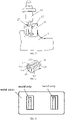
- FIG. 1 and FIG. 2 are structural schematic diagrams of an embodiment of a battery assembly according to the present disclosure.
- the battery assembly includes a circuit board 11, a clamping component 12, and a conductive component 13.
- the clamping component 12 is disposed on the circuit board 11, the clamping component 12 is arranged on a side of the circuit board 11, and the conductive component 13 is inserted into the clamping component 12 to be electrically connected to the circuit board 11 through the clamping component 12.
- the conductive component 13 may be a metal thimble or other component that may be inserted into the clamping component 12, which is not limited in the present disclosure.
- the battery assembly further includes a bracket 14 defining a first accommodating groove 141 and a second accommodating groove 142.
- the circuit board 11 is accommodated in the first accommodating groove 141, and the clamping component 12 is arranged on a side of the circuit board 11 away from a bottom 143 of the first accommodating groove 141, as shown in FIG. 2 .
- a battery core 15 is arranged in the second accommodating groove 142.
- the first accommodating groove 141 and the second accommodating groove 142 are spaced apart with a common sidewall 144 therebetween.
- a sidewall of the first accommodating groove 141 away from the second accommodating groove 142 defines a through hole 18 facing a position of the clamping component 12, and the conductive component 13 is inserted into the clamping component 12 via the through hole 18. That is, the sidewall of the first accommodating groove 141 away from the second accommodating groove 142 forms a connection portion, and the connection portion may be further arranged with a connector such as a magnet component in addition to the conductive component 13.
- a side of the clamping component 12 close to the circuit board 11 may be arranged with a viscous substance.
- the viscous substance may be a conductive adhesive.
- the clamping component 12 is bonded to the circuit board 11 for electrical connection with the circuit board 11.
- the clamping component 12 may be electrically connected to the circuit board 11 through another bonding component.
- the battery assembly may further include a bonding component 16.
- the bonding component 16 is arranged between the clamping component 12 and the circuit board 11 to electrically connect the clamping component 12 to the circuit board 11.
- the bonding component 16 is a viscous conductive material, such as a conductive adhesive or the like, arranged between the circuit board 11 and the clamping component 12 to fix the clamping component 12 on the circuit board 11.
- the clamping component 12 is made of a conductive material such as copper or silver, or an alloy. After the conductive component 13 is inserted into the clamping component 12, the conductive component 13 is electrically connected to the circuit board 11 through the clamping component 12 and the bonding component 16.
- the bonding component 16 may be arranged around the clamping component 12 to bond the clamping component 12 on the circuit board 11.
- a groove configured to accommodate the clamping component 12 may be defined on the circuit board 11. The clamping component 12 is fixed in the groove, thereby being electrically connected to the circuit board 11. in some embodiments, the clamping component 12 is fixed in the groove through the bonding component 16 such as a conductive adhesive, thereby being electrically connected to the circuit board 11.
- the conductive component 13 is a Pogo pin connector.
- a Pogo pin is a spring pin formed by riveting and pre-pressing a pin shaft, a spring, and a pin tube by a precision instrument, to have a precision spring structure in the Pogo pin.
- a surface plating of the Pogo pin is generally made of gold, which may better improve the corrosion resistance, mechanical properties, electrical properties, and the like.
- a pin tip of the Pogo pin may be a pointed needle, a gripping needle, a round needle, a knife-shaped needle, or the like.
- Pogo pin is commonly applied for precision connection in electronic products in field of cell phones, communication, automobiles, medical treatment, aerospace, and the like, which may improve the corrosion resistance, stability, and durability of connectors. Since the Pogo pin is a very fine pin, the Pogo pin applied in a precision connector may reduce weight and volume of the connector, which enables the connector to be more refined and aesthetic.
- the number of the clamping components 12 is two, the number of the conductive components 13 is two, and each conductive component 13 is inserted into a corresponding clamping component 12.
- the clamping component 12 includes a first clamping component 121 and a second clamping component 122
- the conductive component 13 includes a first conductive component 131 and a second conductive component 132.
- the first conductive component 131 is inserted into the first clamping component 121, and the first conductive component 131 is electrically connected to the circuit board 11 through the first clamping component 121 and a corresponding bonding component 16.
- the second conductive component 132 is inserted into the second clamping component 122, and the second conductive component 132 is electrically connected to the circuit board 11 through the second clamping component 122 and a corresponding bonding component 16.
- the clamping component 12 includes a main body 124, a first clamping piece 126, and a second clamping piece 127.
- the main body 124 defines an accommodating cavity 125
- a bottom wall 1253 of the accommodating cavity 125 defines an insertion port 123 for insertion of the conductive component 13.
- the first clamping piece 126 and the second clamping piece 127 are arranged inside the accommodating cavity 125, and are exposed through the insertion port 123.
- a first end of the first clamping piece 126 and a first end of the second clamping piece 127 are disposed close to the insertion port 123, the first end of the first clamping piece 126 is connected to a first sidewall 1251 of the accommodating cavity 125, the first end of the second clamping piece 127 is connected to a second sidewall 1252 of the accommodating cavity 125; and a second end of the first clamping piece 126 and a second end of the second clamping piece 127 are disposed away from the insertion port 123 and extend inside the accommodating cavity 125, so as to form a clamp configured to clamp the conductive component 13.
- a middle part of the first clamping piece 126 is arranged between the first end and the second end of the first clamping piece 126, a middle part of the first clamping piece 127 is arranged between the first end and the second end of the first clamping piece 127.
- the middle part of the first clamping piece 126 is disposed inclined relative to the first sidewall 1251 of the accommodating cavity 125, and the second end of the first clamping piece 126 is bent relative to the middle part of the first clamping piece 126 and is parallel to the first sidewall 1251 of the accommodating cavity 125;
- the middle part of the second clamping piece 127 is disposed inclined relative to the second sidewall 1252 of the accommodating cavity 125, and the second end of the second clamping piece 127 is bent relative to the middle part of the second cl amping piece 127 and is parallel to the second sidewall 1252 of the accommodating cavity 125.
- a distance between the second end of the first clamping piece 126 and the second end of the second clamping piece 127 is less than or equal to an outer diameter of the conductive component 13, so that the clamp may clamp the conductive component 13 when the conductive component 13 is inserted into the clamping component 12.
- a spring may be disposed between the second end of the first clamping piece 126 and the first sidewall 1251 of the accommodating cavity 125, another spring may be disposed between the second end of the second clamping piece 127 and the second sidewall 1252 of the accommodating cavity 125.
- the second end of the first clamping piece 126 is squeezed to move toward the first sidewall 1251 of the accommodating cavity 125 to compress the spring
- the second end of the second clamping piece 127 is squeezed to move toward the second sidewall 1252 of the accommodating cavity 125 to compress the another spring
- the spring and the another spring reversely respectively squeeze the second end of the first clamping piece 126 and the second end of the second clamping piece 127, thereby clamping the conductive component 13 and preventing the conductive component 13 from falling off.
- the first clamping piece 126, the second clamping piece 127, and the main body 124 are in a one-piece structure, and the main body 124 is a hollow tubular body.
- the first sidewall 1251 and the second sidewall 1252 may be arranged as a hollowed-out structure, so that the bonding component 16 may better bond the clamping component 12 on the circuit board 11.
- the clamping component 12 may be form of a rectangular conductive metal piece.
- the rectangular conductive metal piece is cut to form two metal strips configured to form the first clamping piece 126 and the second clamping piece 127, the rectangular conductive metal piece is bent to form a shape as shown in FIG. 4 , and the two metal strips are respectively bent toward an interior of the accommodating cavity 125, thereby forming the first clamping piece 126 and the second clamping piece 127.
- the conductive component 13 is not connected to the circuit board 11 via a wire, but rather is connected to the circuit board 11 via the clamping component 12, so that the battery assembly is simple to assemble, convenient to produce, and has low cost.
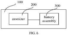
- FIG. 6 is a structural schematic diagram of an electronic atomizing device according to an embodiment of the present disclosure.
- the electronic atomizing device 100 includes an atomizer 200 and a battery assembly 300.
- the battery assembly 300 is configured to supply power to the atomizer 200, and the battery assembly 300 includes the battery assembly shown in any of foregoing embodiments in FIG. 1 to FIG. 3 .
- the conductive component 13 is not connected to the circuit board 11 via a wire, but rather is connected to the circuit board 11 via the clamping component 12, so that the electronic atomizing device is simple to assemble, convenient to produce, and has low cost.
Landscapes
- Chemical & Material Sciences (AREA)
- Chemical Kinetics & Catalysis (AREA)
- Electrochemistry (AREA)
- General Chemical & Material Sciences (AREA)
- Engineering & Computer Science (AREA)
- Life Sciences & Earth Sciences (AREA)
- Biophysics (AREA)
- Computer Hardware Design (AREA)
- Microelectronics & Electronic Packaging (AREA)
- Manufacturing & Machinery (AREA)
- Battery Mounting, Suspending (AREA)
Abstract
Description
- The present disclosure relates to the field of electronic atomizing devices, and in particular, to a battery assembly and an electronic atomizing device.
- In existing electronic atomizing devices, generally, a POGO pin connector is connected to a circuit board via a wire. This configuration has a disadvantage of space waste and high labor cost.
- The present disclosure provides a battery assembly and an electronic atomizing device, as set out in the appended set of claims, which are simple to assemble, convenient to produce, and have low cost.
- Regarding the beneficial effect of the present disclosure, different from the related art, in the battery assembly and the electronic atomizing device provided by the present disclosure, the clamping component is disposed on the circuit board, and the conductive component is inserted into the clamping component to be electrically connected to the circuit board through the clamping component, such that the electronic atomizing device and the battery assembly are simple to assemble, convenient to produce, and have low cost.
- To describe the technical solutions in the embodiments of the present disclosure more clearly, the following briefly describes the accompanying drawings required for describing the embodiments. Apparently, the accompanying drawings in the following description show merely some embodiments of the present disclosure, and a person of ordinary skill in the art may still derive other drawings from these accompanying drawings without creative efforts.
-
FIG. 1 is a cross-sectional structural schematic diagram of a battery assembly according to an embodiment of the present disclosure. -
FIG. 2 is another cross-sectional structural schematic diagram of a battery assembly according to an embodiment of the present disclosure. -
FIG. 3 is a structural schematic diagram of a conductive component and a clamping component according to an embodiment of the present disclosure. -
FIG. 4 is a structural schematic diagram of a clamping component according to an embodiment of the present disclosure. -
FIG. 5 is a schematic diagram of a preparation process of a clamping component according to an embodiment of the present disclosure. -
FIG. 6 is a structural schematic diagram of an electronic atomizing device according to an embodiment of the present disclosure. - The technical solutions in embodiments of this disclosure are clearly and completely described below with reference to accompanying drawings in the embodiments of the present disclosure. Apparently, the embodiments are merely some rather than all of embodiments of the present disclosure. Other embodiments obtained by a person skilled in the art based on the embodiments of the present disclosure without creative efforts shall fall within the scope of the present disclosure.
- The terms "first", "second", and "third" in the present disclosure are used for descriptive purposes only and are not to be construed as indicating or implying relative importance or implicitly indicating the number of technical features indicated. Therefore, features defining "first", "second", and "third" may explicitly or implicitly include at least one of the features. In the description of the present disclosure, "a plurality of" means at least two, such as two and three unless it is specifically defined otherwise. All directional indications (for example, up, down, left, right, front, back) in the embodiments of the present disclosure are only used for explaining relative position relationships, movement situations or the like between various components in a specific condition (as shown in the accompanying drawings). If the specific condition changes, the directional indications change accordingly. In addition, the terms "include", "have", and any variant thereof are intended to cover a non-exclusive inclusion. For example, a process, method, system, product, or device that includes a series of steps or units is not limited to the listed steps or units, but further optionally includes steps or units that are not listed, or further optionally includes another steps or units that are intrinsic to the process, method, product, or device.
- The term "embodiment" mentioned in the specification means that particular features, structures, or characteristics described with reference to embodiments may be included in at least one embodiment of the present disclosure. The term "embodiment" appearing at different positions of the specification may not refer to the same embodiment or an independent or alternative embodiment that is mutually exclusive with another embodiment. A person skilled in the art explicitly or implicitly understands that the embodiments described in the specification may be combined with other embodiments.
- Referring to
FIG. 1 and FIG. 2, FIG. 1 and FIG. 2 are structural schematic diagrams of an embodiment of a battery assembly according to the present disclosure. Specifically, the battery assembly includes acircuit board 11, aclamping component 12, and aconductive component 13. Specifically, theclamping component 12 is disposed on thecircuit board 11, theclamping component 12 is arranged on a side of thecircuit board 11, and theconductive component 13 is inserted into theclamping component 12 to be electrically connected to thecircuit board 11 through theclamping component 12. Theconductive component 13 may be a metal thimble or other component that may be inserted into theclamping component 12, which is not limited in the present disclosure. - Specifically, the battery assembly further includes a
bracket 14 defining a firstaccommodating groove 141 and a secondaccommodating groove 142. Thecircuit board 11 is accommodated in the firstaccommodating groove 141, and theclamping component 12 is arranged on a side of thecircuit board 11 away from abottom 143 of the firstaccommodating groove 141, as shown inFIG. 2 . Abattery core 15 is arranged in the secondaccommodating groove 142. In some embodiments, the firstaccommodating groove 141 and the secondaccommodating groove 142 are spaced apart with acommon sidewall 144 therebetween. Specifically, a sidewall of the firstaccommodating groove 141 away from the secondaccommodating groove 142 defines a throughhole 18 facing a position of theclamping component 12, and theconductive component 13 is inserted into theclamping component 12 via the throughhole 18. That is, the sidewall of the firstaccommodating groove 141 away from the secondaccommodating groove 142 forms a connection portion, and the connection portion may be further arranged with a connector such as a magnet component in addition to theconductive component 13. - In some embodiments, a side of the
clamping component 12 close to thecircuit board 11 may be arranged with a viscous substance. The viscous substance may be a conductive adhesive. Theclamping component 12 is bonded to thecircuit board 11 for electrical connection with thecircuit board 11. In other embodiments, theclamping component 12 may be electrically connected to thecircuit board 11 through another bonding component. Specifically, as shown inFIG. 3 , the battery assembly may further include abonding component 16. Thebonding component 16 is arranged between theclamping component 12 and thecircuit board 11 to electrically connect theclamping component 12 to thecircuit board 11. In some embodiments, thebonding component 16 is a viscous conductive material, such as a conductive adhesive or the like, arranged between thecircuit board 11 and theclamping component 12 to fix theclamping component 12 on thecircuit board 11. Further, theclamping component 12 is made of a conductive material such as copper or silver, or an alloy. After theconductive component 13 is inserted into theclamping component 12, theconductive component 13 is electrically connected to thecircuit board 11 through theclamping component 12 and thebonding component 16. - In some embodiments, the
bonding component 16 may be arranged around theclamping component 12 to bond theclamping component 12 on thecircuit board 11. In other embodiments, a groove configured to accommodate theclamping component 12 may be defined on thecircuit board 11. Theclamping component 12 is fixed in the groove, thereby being electrically connected to thecircuit board 11. in some embodiments, theclamping component 12 is fixed in the groove through thebonding component 16 such as a conductive adhesive, thereby being electrically connected to thecircuit board 11. - In some embodiments, the
conductive component 13 is a Pogo pin connector. A Pogo pin is a spring pin formed by riveting and pre-pressing a pin shaft, a spring, and a pin tube by a precision instrument, to have a precision spring structure in the Pogo pin. A surface plating of the Pogo pin is generally made of gold, which may better improve the corrosion resistance, mechanical properties, electrical properties, and the like. A pin tip of the Pogo pin may be a pointed needle, a gripping needle, a round needle, a knife-shaped needle, or the like. Pogo pin is commonly applied for precision connection in electronic products in field of cell phones, communication, automobiles, medical treatment, aerospace, and the like, which may improve the corrosion resistance, stability, and durability of connectors. Since the Pogo pin is a very fine pin, the Pogo pin applied in a precision connector may reduce weight and volume of the connector, which enables the connector to be more refined and aesthetic. - In some embodiments, the number of the
clamping components 12 is two, the number of theconductive components 13 is two, and eachconductive component 13 is inserted into acorresponding clamping component 12. Specifically, as shown inFIG. 1 , theclamping component 12 includes afirst clamping component 121 and a second clamping component 122, theconductive component 13 includes a firstconductive component 131 and a secondconductive component 132. The firstconductive component 131 is inserted into thefirst clamping component 121, and the firstconductive component 131 is electrically connected to thecircuit board 11 through thefirst clamping component 121 and acorresponding bonding component 16. The secondconductive component 132 is inserted into the second clamping component 122, and the secondconductive component 132 is electrically connected to thecircuit board 11 through the second clamping component 122 and acorresponding bonding component 16. - Specifically, as shown in
FIG. 4 , theclamping component 12 includes amain body 124, afirst clamping piece 126, and asecond clamping piece 127. Themain body 124 defines anaccommodating cavity 125, and abottom wall 1253 of theaccommodating cavity 125 defines aninsertion port 123 for insertion of theconductive component 13. Thefirst clamping piece 126 and thesecond clamping piece 127 are arranged inside theaccommodating cavity 125, and are exposed through theinsertion port 123. A first end of thefirst clamping piece 126 and a first end of thesecond clamping piece 127 are disposed close to theinsertion port 123, the first end of thefirst clamping piece 126 is connected to afirst sidewall 1251 of theaccommodating cavity 125, the first end of thesecond clamping piece 127 is connected to asecond sidewall 1252 of theaccommodating cavity 125; and a second end of thefirst clamping piece 126 and a second end of thesecond clamping piece 127 are disposed away from theinsertion port 123 and extend inside theaccommodating cavity 125, so as to form a clamp configured to clamp theconductive component 13. - Specifically, a middle part of the
first clamping piece 126 is arranged between the first end and the second end of thefirst clamping piece 126, a middle part of thefirst clamping piece 127 is arranged between the first end and the second end of the first clamping piece 127.The middle part of thefirst clamping piece 126 is disposed inclined relative to thefirst sidewall 1251 of theaccommodating cavity 125, and the second end of thefirst clamping piece 126 is bent relative to the middle part of thefirst clamping piece 126 and is parallel to thefirst sidewall 1251 of theaccommodating cavity 125; the middle part of thesecond clamping piece 127 is disposed inclined relative to thesecond sidewall 1252 of theaccommodating cavity 125, and the second end of thesecond clamping piece 127 is bent relative to the middle part of the secondcl amping piece 127 and is parallel to thesecond sidewall 1252 of theaccommodating cavity 125. - Specifically, at a position of the clamp formed by the second end of the
first clamping piece 126 and the second end of thesecond clamping piece 127, a distance between the second end of thefirst clamping piece 126 and the second end of thesecond clamping piece 127 is less than or equal to an outer diameter of theconductive component 13, so that the clamp may clamp theconductive component 13 when theconductive component 13 is inserted into theclamping component 12. - In some embodiments, a spring may be disposed between the second end of the
first clamping piece 126 and thefirst sidewall 1251 of theaccommodating cavity 125, another spring may be disposed between the second end of thesecond clamping piece 127 and thesecond sidewall 1252 of theaccommodating cavity 125. When theconductive component 13 is inserted into theclamping component 12, the second end of thefirst clamping piece 126 is squeezed to move toward thefirst sidewall 1251 of theaccommodating cavity 125 to compress the spring, the second end of thesecond clamping piece 127 is squeezed to move toward thesecond sidewall 1252 of theaccommodating cavity 125 to compress the another spring, the spring and the another spring reversely respectively squeeze the second end of thefirst clamping piece 126 and the second end of thesecond clamping piece 127, thereby clamping theconductive component 13 and preventing theconductive component 13 from falling off. - In some embodiments, the
first clamping piece 126, thesecond clamping piece 127, and themain body 124 are in a one-piece structure, and themain body 124 is a hollow tubular body. In other embodiments, in order to reduce weight of theclamping component 12, thefirst sidewall 1251 and thesecond sidewall 1252 may be arranged as a hollowed-out structure, so that thebonding component 16 may better bond the clampingcomponent 12 on thecircuit board 11. Further, another sidewall to which the opposite two sidewalls of theaccommodating cavity 125 are connected defines a notch or a slit, and the notch or the slit extends along an axial direction of the hollow tubular body, so that sidewalls of the hollow tubular body form a non-closed annulus, which also is conductive to forming theclamping component 12. Specifically, referring toFIG. 5 , theclamping component 12 may be form of a rectangular conductive metal piece. For example, the rectangular conductive metal piece is cut to form two metal strips configured to form thefirst clamping piece 126 and thesecond clamping piece 127, the rectangular conductive metal piece is bent to form a shape as shown inFIG. 4 , and the two metal strips are respectively bent toward an interior of theaccommodating cavity 125, thereby forming thefirst clamping piece 126 and thesecond clamping piece 127. - In the battery assembly of the present disclosure, the
conductive component 13 is not connected to thecircuit board 11 via a wire, but rather is connected to thecircuit board 11 via theclamping component 12, so that the battery assembly is simple to assemble, convenient to produce, and has low cost. - Referring to
FIG. 6, FIG. 6 is a structural schematic diagram of an electronic atomizing device according to an embodiment of the present disclosure. Specifically, theelectronic atomizing device 100 includes anatomizer 200 and abattery assembly 300. Thebattery assembly 300 is configured to supply power to theatomizer 200, and thebattery assembly 300 includes the battery assembly shown in any of foregoing embodiments inFIG. 1 to FIG. 3 . - In the
electronic atomizing device 100 of the present disclosure, theconductive component 13 is not connected to thecircuit board 11 via a wire, but rather is connected to thecircuit board 11 via theclamping component 12, so that the electronic atomizing device is simple to assemble, convenient to produce, and has low cost.
Claims (10)
- A battery assembly (300), characterized by comprising:a circuit board (11);a clamping component (12), disposed on the circuit board (11); anda conductive component (13), inserted into the clamping component (12) and electrically connected to the circuit board (11) through the clamping component (12).
- The battery assembly (300) according to claim 1, further comprising:
a bracket (14), defining a first accommodating groove (141), wherein the circuit board (11) is accommodated in the first accommodating groove (141), the clamping component (12) is arranged on a side of the circuit board (11) away from a bottom (143) of the first accommodating groove (141). - The battery assembly (300) according to claim 1 or 2, wherein a viscous substance is arranged on a side of the clamping component (12) close to the circuit board (11), the viscous substance is configured to electrically connect the clamping component (12) to the circuit board (11); or
the battery assembly (300) further comprises:
a bonding component (16), arranged between the clamping component (12) and the circuit board (11) to electrically connect the clamping component (12) to the circuit board (11). - The battery assembly (300) according to claim 2, wherein the bracket (14) further defines a second accommodating groove (142) configured to accommodate a battery core (15), the first accommodating groove (141) and the second accommodating groove (142) are spaced apart;
a sidewall of the first accommodating groove (141) away from the second accommodating groove (142) defines a through hole (18) facing the clamping component (12), and the conductive component (13) is inserted into the clamping component (12) through the through hole (18). - The battery assembly (300) according to any one of claims 1 to 4, wherein the number of the clamping components (12) is two, the number of the conductive components (13) is two, and each the conductive component (13) is inserted into a corresponding clamping component (12).
- The battery assembly (300) according to claim 1, wherein the clamping component (12) comprises a main body (124), a first clamping piece (126) and a second clamping piece (127);the main body (124) defines an accommodating cavity (125), a bottom wall (1253) of the accommodating cavity (125) defines an insertion port (123), and the conductive component (13) is inserted through the insertion port (123); the first clamping piece (126) and the second clamping piece (127) are arranged in the accommodating cavity (125) and exposed through the insertion port (123);a first end of the first clamping piece (126) and a first end of the second clamping piece (127) are disposed close to the insertion port (123), the first end of the first clamping piece (126) is connected to a first sidewall (1251) of the accommodating cavity (125), the first end of the second clamping piece (127) is connected to a second sidewall (1252) of the accommodating cavity (125); and a second end of the first clamping piece (126) and a second end of the second clamping piece (127) are disposed away from the insertion port (123) and extend inside the accommodating cavity (125), so as to form a clamp configured to clamp the conductive component (13).
- The battery assembly according to claim 6, wherein the first clamping piece, the second clamping piece, and the main body are in a one-piece structure.
- The battery assembly (300) according any one of claims 6 or 7, wherein a middle part between the first end and the second end of the first clamping piece (126) is disposed inclined relative to the first sidewall (1251) of the accommodating cavity (125), and the second end of the first clamping piece (126) is bent relative to the middle part of the first clamping piece (126) and is parallel to the first sidewall (1251) of the accommodating cavity (125); a middle part between the first end and the second end of the second clamping piece (127) is disposed inclined relative to the second sidewall (1252) of the accommodating cavity (125), and the second end of the second clamping piece (127) is bent relative to the middle part of the second clamping piece (127) and is parallel to the second sidewall (1252) of the accommodating cavity (125).
- The battery assembly (300) according to any one of claims 6 to 8, wherein the main body (124) is a hollow tubular body, the first sidewall (1251) and the second sidewall (1252) are in a hollowed-out structure.
- An electronic atomizing device (100), characterized by comprising:an atomizer (200); andthe battery assembly (300) according to any one of claims 1 to 9, configured to supply power to the atomizer (200).
Applications Claiming Priority (1)
| Application Number | Priority Date | Filing Date | Title |
|---|---|---|---|
| CN202110609740.5A CN113383999A (en) | 2021-06-01 | 2021-06-01 | Battery pack and electronic atomization device |
Publications (2)
| Publication Number | Publication Date |
|---|---|
| EP4099491A2 true EP4099491A2 (en) | 2022-12-07 |
| EP4099491A3 EP4099491A3 (en) | 2023-06-21 |
Family
ID=77619799
Family Applications (1)
| Application Number | Title | Priority Date | Filing Date |
|---|---|---|---|
| EP22176446.7A Pending EP4099491A3 (en) | 2021-06-01 | 2022-05-31 | Battery assembly and electronic atomizing device |
Country Status (3)
| Country | Link |
|---|---|
| US (1) | US20220378094A1 (en) |
| EP (1) | EP4099491A3 (en) |
| CN (1) | CN113383999A (en) |
Families Citing this family (3)
| Publication number | Priority date | Publication date | Assignee | Title |
|---|---|---|---|---|
| CN113384004B (en) * | 2021-06-01 | 2025-03-14 | 深圳麦克韦尔科技有限公司 | A battery assembly for electronic atomization device and electronic atomization device |
| CN113383999A (en) * | 2021-06-01 | 2021-09-14 | 深圳麦克韦尔科技有限公司 | Battery pack and electronic atomization device |
| US12607335B1 (en) * | 2025-05-21 | 2026-04-21 | Zhejiang Lvshang Optoelectronics Technology Co., Ltd | Power supply for light string |
Family Cites Families (11)
| Publication number | Priority date | Publication date | Assignee | Title |
|---|---|---|---|---|
| US6410176B1 (en) * | 2000-07-31 | 2002-06-25 | Plug Power, Inc. | Voltage monitoring system for a fuel cell stack |
| CN202649535U (en) * | 2012-07-06 | 2013-01-02 | 河北华美光电子有限公司 | QSFP optical module housing structure |
| WO2018080181A1 (en) * | 2016-10-26 | 2018-05-03 | 삼성에스디아이 주식회사 | Connector for printed circuit board and battery system comprising printed circuit board and connector |
| TWM548891U (en) * | 2017-06-30 | 2017-09-11 | Apo International Co Ltd | Rechargeable Battery |
| DE102018127926A1 (en) * | 2018-07-09 | 2020-01-09 | Hauni Maschinenbau Gmbh | Vaporizer head for an inhaler, especially for an electronic cigarette product |
| CN110752464B (en) * | 2018-07-23 | 2020-12-04 | 映兴电子股份有限公司 | Conductive terminal structure of connector |
| CN112841732B (en) * | 2021-02-02 | 2025-09-05 | 深圳麦克韦尔科技有限公司 | Electronic atomization device, power supply assembly and bracket assembly |
| CN112841730B (en) * | 2021-02-02 | 2025-07-08 | 深圳麦克韦尔科技有限公司 | Electronic atomization device, power supply assembly thereof and bracket assembly |
| CN112841731B (en) * | 2021-02-02 | 2025-09-05 | 深圳麦克韦尔科技有限公司 | Electronic atomization device and power supply component thereof |
| CN215775537U (en) * | 2021-06-01 | 2022-02-11 | 深圳麦克韦尔科技有限公司 | Battery pack and electronic atomization device |
| CN113383999A (en) * | 2021-06-01 | 2021-09-14 | 深圳麦克韦尔科技有限公司 | Battery pack and electronic atomization device |
-
2021
- 2021-06-01 CN CN202110609740.5A patent/CN113383999A/en active Pending
-
2022
- 2022-05-25 US US17/824,089 patent/US20220378094A1/en not_active Abandoned
- 2022-05-31 EP EP22176446.7A patent/EP4099491A3/en active Pending
Also Published As
| Publication number | Publication date |
|---|---|
| CN113383999A (en) | 2021-09-14 |
| EP4099491A3 (en) | 2023-06-21 |
| US20220378094A1 (en) | 2022-12-01 |
Similar Documents
| Publication | Publication Date | Title |
|---|---|---|
| EP4099491A2 (en) | Battery assembly and electronic atomizing device | |
| US9172194B2 (en) | Coaxial connector plug | |
| US9673546B2 (en) | Cable holding member, electrical connection device, connector device, flat cable | |
| CN204927620U (en) | Connector device | |
| CN215775537U (en) | Battery pack and electronic atomization device | |
| US20120040546A1 (en) | Very High Frequency Electrical Connector | |
| KR20110013369A (en) | Connection member | |
| CN205830156U (en) | Flexible circuit board, connector and battery signal sampling device | |
| CN210040663U (en) | Cable connector | |
| CN203466326U (en) | Probe type connection terminal | |
| CN219696713U (en) | Wire harness assembly | |
| CN216252913U (en) | Camera device | |
| JP2014232755A (en) | Choke coil | |
| US7249970B1 (en) | Connector for coaxial cable | |
| US10436816B2 (en) | Test coaxial connector | |
| CN216250345U (en) | Inductor | |
| CN217655177U (en) | Universal meter measuring wire and measuring assembly | |
| CN217281538U (en) | Precision testing coaxial connector based on 5GPCB (gigabit passive coax B) board end connector | |
| CN221379857U (en) | Binding post and connector | |
| CN223023755U (en) | Connector terminal | |
| CN115911933B (en) | A radio frequency coaxial connector | |
| CN216085418U (en) | Plate end connector | |
| CN217280604U (en) | Reed with manganin | |
| CN221057712U (en) | Integrated MINI FAKRA connector | |
| CN220155785U (en) | Plug inner frame and plug |
Legal Events
| Date | Code | Title | Description |
|---|---|---|---|
| PUAI | Public reference made under article 153(3) epc to a published international application that has entered the european phase |
Free format text: ORIGINAL CODE: 0009012 |
|
| STAA | Information on the status of an ep patent application or granted ep patent |
Free format text: STATUS: THE APPLICATION HAS BEEN PUBLISHED |
|
| AK | Designated contracting states |
Kind code of ref document: A2 Designated state(s): AL AT BE BG CH CY CZ DE DK EE ES FI FR GB GR HR HU IE IS IT LI LT LU LV MC MK MT NL NO PL PT RO RS SE SI SK SM TR |
|
| RIC1 | Information provided on ipc code assigned before grant |
Ipc: H01R 12/70 20110101ALI20230130BHEP Ipc: H01M 10/42 20060101ALI20230130BHEP Ipc: H01M 50/284 20210101ALI20230130BHEP Ipc: H01M 50/262 20210101ALI20230130BHEP Ipc: A24F 40/40 20200101ALI20230130BHEP Ipc: H01M 50/247 20210101AFI20230130BHEP |
|
| PUAL | Search report despatched |
Free format text: ORIGINAL CODE: 0009013 |
|
| AK | Designated contracting states |
Kind code of ref document: A3 Designated state(s): AL AT BE BG CH CY CZ DE DK EE ES FI FR GB GR HR HU IE IS IT LI LT LU LV MC MK MT NL NO PL PT RO RS SE SI SK SM TR |
|
| RIC1 | Information provided on ipc code assigned before grant |
Ipc: H01R 12/70 20110101ALI20230515BHEP Ipc: H01M 10/42 20060101ALI20230515BHEP Ipc: H01M 50/284 20210101ALI20230515BHEP Ipc: H01M 50/262 20210101ALI20230515BHEP Ipc: A24F 40/40 20200101ALI20230515BHEP Ipc: H01M 50/247 20210101AFI20230515BHEP |
|
| STAA | Information on the status of an ep patent application or granted ep patent |
Free format text: STATUS: REQUEST FOR EXAMINATION WAS MADE |
|
| 17P | Request for examination filed |
Effective date: 20231102 |
|
| RBV | Designated contracting states (corrected) |
Designated state(s): AL AT BE BG CH CY CZ DE DK EE ES FI FR GB GR HR HU IE IS IT LI LT LU LV MC MK MT NL NO PL PT RO RS SE SI SK SM TR |
|
| RAP3 | Party data changed (applicant data changed or rights of an application transferred) |
Owner name: SHENZHEN SMOORE TECHNOLOGY LIMITED |
|
| RAP3 | Party data changed (applicant data changed or rights of an application transferred) |
Owner name: SHENZHEN SMOORE TECHNOLOGY LIMITED |