EP4099070B1 - Thermal interface structures for optical communication devices - Google Patents
Thermal interface structures for optical communication devices Download PDFInfo
- Publication number
- EP4099070B1 EP4099070B1 EP22158792.6A EP22158792A EP4099070B1 EP 4099070 B1 EP4099070 B1 EP 4099070B1 EP 22158792 A EP22158792 A EP 22158792A EP 4099070 B1 EP4099070 B1 EP 4099070B1
- Authority
- EP
- European Patent Office
- Prior art keywords
- integrated circuit
- thermal interface
- photonic integrated
- circuit device
- interface material
- Prior art date
- Legal status (The legal status is an assumption and is not a legal conclusion. Google has not performed a legal analysis and makes no representation as to the accuracy of the status listed.)
- Active
Links
Images


Classifications
-
- G—PHYSICS
- G02—OPTICS
- G02B—OPTICAL ELEMENTS, SYSTEMS OR APPARATUS
- G02B6/00—Light guides; Structural details of arrangements comprising light guides and other optical elements, e.g. couplings
- G02B6/24—Coupling light guides
- G02B6/42—Coupling light guides with opto-electronic elements
- G02B6/4201—Packages, e.g. shape, construction, internal or external details
- G02B6/4266—Thermal aspects, temperature control or temperature monitoring
- G02B6/4268—Cooling
-
- G—PHYSICS
- G02—OPTICS
- G02B—OPTICAL ELEMENTS, SYSTEMS OR APPARATUS
- G02B6/00—Light guides; Structural details of arrangements comprising light guides and other optical elements, e.g. couplings
- G02B6/24—Coupling light guides
- G02B6/42—Coupling light guides with opto-electronic elements
- G02B6/4201—Packages, e.g. shape, construction, internal or external details
- G02B6/4204—Packages, e.g. shape, construction, internal or external details the coupling comprising intermediate optical elements, e.g. lenses, holograms
- G02B6/4206—Optical features
-
- G—PHYSICS
- G02—OPTICS
- G02B—OPTICAL ELEMENTS, SYSTEMS OR APPARATUS
- G02B6/00—Light guides; Structural details of arrangements comprising light guides and other optical elements, e.g. couplings
- G02B6/24—Coupling light guides
- G02B6/42—Coupling light guides with opto-electronic elements
- G02B6/4201—Packages, e.g. shape, construction, internal or external details
- G02B6/4266—Thermal aspects, temperature control or temperature monitoring
- G02B6/4268—Cooling
- G02B6/4269—Cooling with heat sinks or radiation fins
-
- G—PHYSICS
- G02—OPTICS
- G02B—OPTICAL ELEMENTS, SYSTEMS OR APPARATUS
- G02B6/00—Light guides; Structural details of arrangements comprising light guides and other optical elements, e.g. couplings
- G02B6/24—Coupling light guides
- G02B6/42—Coupling light guides with opto-electronic elements
- G02B6/43—Arrangements comprising a plurality of opto-electronic elements and associated optical interconnections
Definitions
- Embodiments of the present description generally relate to the field of integrated circuit assemblies and, more particularly, to the integration of thermal interface structures for the removal of heat from optical communication devices.
- the integrated circuit industry is continually striving to produce ever faster and smaller integrated circuit devices for use in various server and mobile electronic products, including, but not limited to, computer server products and portable products, such as wearable integrated circuit systems, portable computers, electronic tablets, cellular phones, digital cameras, and the like.
- optical interconnects are being used to replace electrical interconnects, as optical interconnects offer very high bandwidths compared to electrical interconnects.
- photonic integrated circuit devices are used to convert electrical signals to optical signals.
- photonic integrated circuit devices may have lasing components, amplifiers, and/or other electrical circuits which generate significant power densities (e.g., about 50 to 150 watts per square millimeter compared to a processing or computing device which may have power densities of about 5 to 50 watts per square millimeter, depending on use condition).
- optical components, such as lasers can typically only tolerate a maximum temperature of between about 70 and 90 degrees Celsius compared to the maximum junction temperatures on processing or computing devices of between about 100 to 110 degrees Celsius.
- thermal interface materials to the integrated circuit devices within the integrated may be greases, gels, pads, films, and the like, with a high loading of thermally conductive filler materials, such as metal and/or ceramic particles.
- thermal interface materials may not be compatible with photonic integrated circuit devices.
- the silicon substrate, from which the device is made must be thinned in order to remove silicon in areas where optical waveguides are located to ensure that the optical beam stays in the waveguide and does not couple with the silicon substrate, as will be understood to those skilled in the art.
- the silicon photonic integrated circuit devices need to be thermally coupled to the heat dissipation device in order to maintain an acceptable operating temperature. The required thinning of the silicon photonic integrated circuit devices will bring the thermal interface materials into close proximity with the waveguides of the silicon photonic integrated circuit devices.
- thermally conductive fillers in the thermal interface materials will absorb, scatter, and/or couple the light from the waveguides, resulting in significant waveguide insertion loss and sometimes even "optical blindness" where no light comes out of the waveguide at all.
- cooling photonic integrated circuit devices is a significant challenge.
- US2014348462 A1 describes an optical circuit board including a top face, a bottom face, an optical layer buried between bottom and top faces, the optical layer being adapted to transmit optical signals, an opto-electronic component adapted to emit or receive light transmitted through the optical layer, a solid heat dissipative element adapted to dissipate heat generated at the opto-electronic component.
- WO9633441 A1 describes an asymmetric thermo-optical device comprising a waveguiding structure which comprises at least one input light path and a first output light path and a second output light path, the second output light path having a smaller width than the first output light path, and the first output light path being provided with a first heating element, wherein the second output light path is provided with a second heating element.
- the second heating element is connected to a capacitor which is connected in parallel with the first heating element.
- WO2007103880 A2 describes a tunable optical waveguide chip for optical transforms.
- the chip includes a planar waveguide having a lens region and a plurality of individually addressable energy applicators distributed transversely across an optical path through the lens region.
- a desired index of refraction profile can be induced in the lens region transversely across the optical path for performing any of a variety of optical transforms.
- the device may include an upstream AWG which focus a wavelength de-multiplexed signal on a focal plane within the lens region.
- the applicators may be thermo-optic or electro-optic, for example.
- US2002018636 A1 describes a device for variable attenuation of an optical channel which includes an elongated core surrounded by a cladding.
- the device further includes a thermal source arranged above the core.
- the thermal source is operable to generate a temperature gradient of controllable magnitude along a vertical axis extending through the core. The temperature gradient causes reduction of the local refractive index within the core relative to surrounding regions of the cladding such that a portion of the optical energy is deflected away from the thermal source and extracted from the core.
- JP2020134599 A describes an optical semiconductor element which comprises a substrate, an optical waveguide structure including an optical waveguiding layer and a cladding part formed above the substrate; a heater thermally connected to the optical waveguide structure; conductor wiring electrically connected to the heater; and an electrode pad electrically connected to the conductor wiring.
- the conductor wiring has a small structure such that a portion positioned in the vicinity of the heater has a cross sectional area smaller than a cross sectional area of a portion positioned close to the electrode pad.
- US 2003/223697 A1 describes an apparatus comprising a photonic integrated circuit device, a thermal interface material and a heat dissipation device. The invention is set forth in independent claim 1. Embodiments of the invention described in the dependent claims.
- over, “to”, “between” and “on” as used herein may refer to a relative position of one layer with respect to other layers.
- One layer “over” or “on” another layer or bonded “to” another layer may be directly in contact with the other layer or may have one or more intervening layers.
- One layer “between” layers may be directly in contact with the layers or may have one or more intervening layers.
- the term "package” generally refers to a self-contained carrier of one or more dice, where the dice are attached to the package substrate, and may be encapsulated for protection, with integrated or wire-bonded interconnects between the dice and leads, pins or bumps located on the external portions of the package substrate.
- the package may contain a single die, or multiple dice, providing a specific function.
- the package is usually mounted on a printed circuit board for interconnection with other packaged integrated circuits and discrete components, forming a larger circuit.
- the term “cored” generally refers to a substrate of an integrated circuit package built upon a board, card or wafer comprising a non-flexible stiff material.
- a small printed circuit board is used as a core, upon which integrated circuit device and discrete passive components may be soldered.
- the core has vias extending from one side to the other, allowing circuitry on one side of the core to be coupled directly to circuitry on the opposite side of the core.
- the core may also serve as a platform for building up layers of conductors and dielectric materials.
- coreless generally refers to a substrate of an integrated circuit package having no core.
- the lack of a core allows for higher-density package architectures, as the through-vias have relatively large dimensions and pitch compared to high-density interconnects.
- dielectric generally refers to any number of non-electrically conductive materials that make up the structure of a package substrate.
- dielectric material may be incorporated into an integrated circuit package as layers of laminate film or as a resin molded over integrated circuit dice mounted on the substrate.
- the term "metallization” generally refers to metal layers formed over and through the dielectric material of the package substrate.
- the metal layers are generally patterned to form metal structures such as traces and bond pads.
- the metallization of a package substrate may be confined to a single layer or in multiple layers separated by layers of dielectric.
- bond pad generally refers to metallization structures that terminate integrated traces and vias in integrated circuit packages and dies.
- soldder pad may be occasionally substituted for "bond pad” and carries the same meaning.
- solder bump generally refers to a solder layer formed on a bond pad.
- the solder layer typically has a round shape, hence the term “solder bump”.
- the term “substrate” generally refers to a planar platform comprising dielectric and metallization structures.
- the substrate mechanically supports and electrically couples one or more IC dies on a single platform, with encapsulation of the one or more IC dies by a moldable dielectric material.
- the substrate generally comprises solder bumps as bonding interconnects on both sides.
- One side of the substrate generally referred to as the “die side”
- the opposite side of the substrate generally referred to as the "land side” comprises solder bumps for bonding the package to a printed circuit board.
- the term "assembly” generally refers to a grouping of parts into a single functional unit.
- the parts may be separate and are mechanically assembled into a functional unit, where the parts may be removable.
- the parts may be permanently bonded together.
- the parts are integrated together.
- connection means a direct connection, such as electrical, mechanical, or magnetic connection between the things that are connected, without any intermediary devices.
- Coupled means a direct or indirect connection, such as a direct electrical, mechanical, magnetic or fluidic connection between the things that are connected or an indirect connection, through one or more passive or active intermediary devices.
- circuit or “module” may refer to one or more passive and/or active components that are arranged to cooperate with one another to provide a desired function.
- signal may refer to at least one current signal, voltage signal, magnetic signal, or data/clock signal.
- phrases “A and/or B” and “A or B” mean (A), (B), or (A and B).
- phrase “A, B, and/or C” means (A), (B), (C), (A and B), (A and C), (B and C), or (A, B and C).
- cross-sectional Views labeled "cross-sectional”, “profile” and “plan” correspond to orthogonal planes within a cartesian coordinate system. Thus, cross-sectional and profile views are taken in the x-z plane, and plan views are taken in the x-y plane. Typically, profile views in the x-z plane are cross-sectional views. Where appropriate, drawings are labeled with axes to indicate the orientation of the figure.
- Embodiments of the present description relate to the removal of heat from a silicon photonic integrated circuit device, wherein the removal of heat is facilitated with an optically compatible thermal interface structure thereon.
- the thermal interface structures may comprise stack-up designs, including an optical isolation structure and a thermal interface material, which reduces light coupling effects, while effectively conducting heat from the silicon photonic integrated circuit device to a heat dissipation device, thereby allowing effective management of the temperature thereof.
- FIG. 1 illustrates an electronic assembly 100, such as an integrated circuit package.
- the electronic assembly 100 may include at least one silicon photonic integrated circuit device 200 electrically attached to a package substrate 110, wherein each silicon photonic integrated circuit device 200 may have an optical communication cable 150, such as an optic fiber cable, attached thereto.
- the package substrate 110 may be any appropriate structure, including, but not limited to, an interposer.
- the package substrate 110 may have a first surface 112, an opposing second surface 114, and at least one side 116 extending between the first surface 112 and the second surface 114.
- the silicon photonic integrated circuit devices 200 may be attached proximate the side(s) 116 of the package substrate 110 to allow for easier attachment access for the optical communication cable 150.
- a plurality of additional integrated circuit devices 210, 220, and 230 may also be electrically attached to the package substrate 110.
- Each of the additional integrated circuit devices 210, 220, and 230 may be any appropriate device, including, but not limited to, a microprocessor, a chipset, a graphics device, a wireless device, a memory device, an application specific integrated circuit, a transceiver device, an input/output device, combinations thereof, stacks thereof, or the like.
- integrated circuit device(s) 210 may be input/output control hubs (such as electronic integrated chips), integrated circuit device(s) 220 may be processing units, and integrated circuit device(s) 230 may be cache memory devices.
- At least one of the integrated circuit devices 200, 210, 220, and 230 may be electrically attached to the package substrate 110 in a configuration generally known as a flip-chip or controlled collapse chip connection ("C4") configuration.
- the silicon photonic integrated circuit devices 200 may be electrically attached to the package substrate 110 in an "open cavity" configuration, wherein the silicon photonic integrated circuit devices 200 are at least partially embedded in the package substrate 110 that allows for direct attachment of the silicon photonic integrated circuit devices 200 to electronic integrated chips 210 (a controller for the silicon photonic integrated circuit devices 200) for better power efficiency and allows for less obstructed access to the silicon photonic integrated circuit device for the attachment of the optical communication cables 150.
- the package substrate 110 may comprise a plurality of dielectric material layers (not shown), which may include build-up films and/or solder resist layers, and may be composed of an appropriate dielectric material, including, but not limited to, bismaleimide triazine resin, fire retardant grade 4 material, polyimide material, silica filled epoxy material, glass reinforced epoxy material, low temperature co-fired ceramic materials, and the like, as well as low-k and ultra low-k dielectrics (dielectric constants less than about 3.6), including, but not limited to, carbon doped dielectrics, fluorine doped dielectrics, porous dielectrics, organic polymeric dielectrics, fluoropolymers, and the like.
- an appropriate dielectric material including, but not limited to, bismaleimide triazine resin, fire retardant grade 4 material, polyimide material, silica filled epoxy material, glass reinforced epoxy material, low temperature co-fired ceramic materials, and the like, as well as low-k and ultra low-k dielectrics (dielectric constants less
- the package substrate 110 may further include conductive routes or "metallization" (not shown) extending through the package substrate 110 for the interconnection of the integrated circuit devices 200, 210, 220, and 230 and/or for the interconnection of the package substrate 110 to an external board (not shown).
- These conductive routes (not shown) may be a combination of conductive traces (not shown) formed between the dielectric material layers (not shown) and conductive vias (not shown) extending through the dielectric material layers (not shown).
- conductive routes may be a combination of conductive traces (not shown) formed between the dielectric material layers (not shown) and conductive vias (not shown) extending through the dielectric material layers (not shown).
- the structure and fabrication of conductive traces and conductive vias are well known in the art and are not shown or described for purposes of clarity and conciseness.
- the conductive traces and the conductive vias may be made of any appropriate electrically conductive material, including, but not limited to, metals, such as copper, silver, nickel, gold, and aluminum, alloys thereof, and the like.
- the package substrate 110 may be a cored substrate or a coreless substrate.
- the package substrate 110 may include a heat dissipation device 300 disposed thereon, wherein the heat dissipation device 300 may be thermally coupled to the integrated circuit devices 200, 210, 220, and 230 with one or more thermal interface materials (not shown).
- the thermal interface materials for the "non-photonic" integrated circuit devices such as integrated circuit devices 210, 220, and 230, may be thermally coupled to the heat dissipation device 300 with standard thermal interface materials with a high loading of thermally conductive filler materials, such as metal and/or ceramic particles.
- thermal interface materials may not be compatible with the silicon photonic integrated circuit devices 200.
- the embodiments of the present description are directed to thermal interface structures for these photonic integrated circuit devices 200.
- the heat dissipation device 300 may comprise any appropriate thermally conductive structure, including but not limited to an integrated heat spreader, a heat sink, a heat pipe, a thermoelectric cooler, a cold plate, and the like, and may be made of any appropriate thermally conductive material, including, but not limited to, metals, such as copper, silver, nickel, gold, and aluminum, alloys thereof, and the like.
- the heat dissipation device 300 may include a cut-out window or notch therein to allow for a less obstructed access to the silicon photonic integrated circuit device for the attachment of the optical communication cables 150.
- FIGs. 3-8 illustrate side cross-sectional views of embodiments of the present description. It is noted that various processes and techniques for the electrical attachment of a photonic integrated circuit device to a package substrate is well known in the art and, thus, for the sake of clarity and conciseness will not be discussed nor will the package substrate be illustrated.
- the silicon photonic integrated circuit device 200 may be formed having a first surface 202 and an opposing second surface 204.
- the first surface 202 may contain active circuitry (not shown), active structures (not shown), communication structures (not shown - such as waveguides, grating couplers, and the like), interconnection structures (not shown - such as bond pads, and structures (not shown - e.g., sockets, clips, plugs and the like) for connection of the optical communication cable 150.
- the entire silicon photonic integrated circuit device 200 may be thinned, such as by etching, to a thickness T1 of between about 10 and 20 microns.
- a thermal interface structure 400 may then be formed on the silicon photonic integrated circuit device 200.
- the thermal interface structure 400 may comprise an optical isolation structure, such as a light insulating die attach film 410, a silicon heat spreader 420, and a thermal interface material layer 430.
- the light insulating die attach film 410 may be formed abutting the first surface 202 of the silicon photonic integrated circuit device 200.
- the light insulating die attach film 410 may be any appropriate adhesive which does not significantly absorb, scatter, and/or couple light (photons) from the communication structures on the first surface 202.
- the light insulating die attach film 410 may include, but is not limited to, silicones, acrylates, epoxies, rubbers, fused silicas, acrylics, and the like.
- the light insulating die attach film 410 includes silica filler particles. When the refraction index of the light insulating die attach film 410 substantially matches the refraction index of the silica filler particles, the light insulating die attach film 410 is substantially optically transparent.
- the light insulating die attach film 410 may have a thickness T2 of between about 5 and 20 microns, but not limited thereto.
- the rule of thumb is that the minimum thickness T2 needs to be at least two times larger than the mode field diameter of communication structures on the first surface 202 in order to effectively insulate light.
- the maximum thickness T2 of the light insulation die attach film 410 will depend on desired parameter goals. For example, as the thermal conductivity of die attach films are typically relatively low (e.g., between about 0.2 and 0.4 watts per meter*Kelvin), a thinner film closer to 5 microns may result in a lower thermal resistance and may be preferred in most cases for more efficient heat removal. However, in order to accommodate larger packages and potential warpage, a thicker film of closer to 20 microns may be chosen to accommodate such warpage.
- the silicon heat spreader 420 may contact the light insulating die attach film 410 to adhere it to the silicon photonic integrated circuit device 200 for improved heat removal. As the light insulating die attach film 410 optically isolates the first surface 202 of the silicon photonic integrated circuit device 200, the silicon heat spreader 420 will not cause light absorption, scattering, and/or coupling. Furthermore, the silicon heat spreader 420 will have substantially the same coefficient of thermal expansion as the silicon photonic integrated circuit device 200 to minimize thermally induced mechanical stresses that could damage components of the silicon photonic integrated circuit device 200.
- the thermal interface material layer 430 may be disposed between the silicon heat spreader 420 and the heat dissipation device 300 for thermal coupling therebetween. As the thermal interface material layer 430 is between the silicon heat spreader 420 and the heat dissipation device 300, and does not contact the silicon photonic integrated circuit device, the thermal interface material layer 430 may be any appropriate thermally conductive material, filled or unfilled.
- the light insulative die attach film 410 may be pre-attached to the silicon heat spreader 420 for easier handling.
- the thermal interface material layer 430 may be pre-attached to heat dissipation device 300 to eliminate a step of pick and place.
- a thermal interface structure 500 may comprise an optical isolation structure, such as an air gap 270 formed in a silicon plateau 510 of the silicon photonic integrated circuit device 200, and a thermal interface material, such as a compliant thermal interface pad 520.
- the silicon photonic integrated circuit device 200 may be thinned by selective etching to form the first surface 202, such that the at least one silicon plateau 510 extends from the first surface 202.
- the selective etching forms the air gap 270 within the silicon plateau 510 in at least one area 260 where at least one waveguide is formed, and removes silicon in at least one area 250 where a grating coupler is formed (i.e., area for the attachment of the optical communication cable 150), which results in the formation of the at least one silicon plateau 510.
- the silicon plateau 510 may have a thickness T3 of between about 100 and 200 microns for heat spreading.
- the air gap 270 in at least one area 260 prevents light absorption, scattering, and/or coupling, as will be understood to those skilled in the art.
- the compliant thermal interface pad 520 may be disposed between the silicon plateau 510 of the silicon photonic integrated circuit device 200 and the heat dissipation device 300.
- the compliant thermal interface pad 520 is sufficiently conformable, resilient, and/or deformable is to reduce loading stress from the heat dissipation device 300 to the silicon photonic integrated circuit device 200, which may damage components within the silicon photonic integrated circuit device 200 or even crack the silicon photonic integrated circuit device 200 itself.
- the compliant thermal interface pad 520 may be sufficiently rigid to prevent it from extending too far into the air gap 270 over the waveguide area 260.
- the compliant thermal interface pad 520 may partially extend into the air gap 270, as long as there is a distance of two times the "mode field diameter (MFD)" between the first surface 202 over the waveguide area 260 and the thermal interface pad 520.
- the compliant thermal interface pad 520 may include, but is not limited to, gap filler material (such as silicone rubber carrier material containing thermally conductive ceramic filler particles), thermally conductive elastomer, vertical carbon thermal interface material, and the like.
- a thermal interface structure 600 may be formed between the silicon photonic integrated circuit device 200 and the heat dissipation device 300.
- the thermal interface structure 600 may comprise an optical isolation structure, such as a cladding material layer 610, and a thermal interface material layer, such as a thermal interface tape 620.
- the cladding material layer 610 may be formed abutting the first surface 202 of the silicon photonic integrated circuit device 200.
- the cladding material layer 610 may be any appropriate material which does not significantly absorb, scatter, and/or couple light (photons).
- the cladding material layer 610 includes silicones, acrylates, epoxies or acrylics.
- the cladding material layer 610 may be substantially transparent. In another embodiment of the present description, the cladding material layer 610 may have a refraction index between about 1.3 and 1.5. In a further embodiment of the present description, the cladding material layer 610 may have a thickness T4 of between about 2 and 3 times the mode field diameter of connection structures, such as waveguides, within the silicon photonic integrated circuit device 200.
- the thermal interface tape 620 may include, but is not limited to, gap filler material (such as silicone rubber carrier material containing thermally conductive ceramic filler particles), thermally conductive elastomer, vertical carbon thermal interface material, and the like.
- the thermal interface tape 620 can be replaced by thermal grease or a polymer thermal interface material.
- the thermal interface structure 600 may be pre-attached to the heat dissipation device 300 for easier handling, as shown in FIG. 6 .
- the thermal interface structure i.e., the combination of the cladding material layer 610 and the thermal interface tape 620 may be supplied as a stand-alone product, as shown in FIG. 7 .
- the cladding material layer 610 may be pre-attached to the silicon photonic integrated circuit device 200, as shown in FIG. 8 .
- FIG. 9 illustrates an electronic or computing device 700 in accordance with one implementation of the present description.
- the computing device 700 may include a housing 701 having a board 702 disposed therein.
- the computing device 700 may include a number of integrated circuit components, including but not limited to a processor 704, at least one communication chip 706A, 706B, volatile memory 708 (e.g., DRAM), non-volatile memory 710 (e.g., ROM), flash memory 712, a graphics processor or CPU 714, a digital signal processor (not shown), a crypto processor (not shown), a chipset 716, an antenna, a display (touchscreen display), a touchscreen controller, a battery, an audio codec (not shown), a video codec (not shown), a power amplifier (AMP), a global positioning system (GPS) device, a compass, an accelerometer (not shown), a gyroscope (not shown), a speaker, a camera, and a mass storage device (not shown) (such
- the communication chip enables wireless communications for the transfer of data to and from the computing device.
- wireless and its derivatives may be used to describe circuits, devices, systems, methods, techniques, communications channels, etc., that may communicate data through the use of modulated electromagnetic radiation through a non-solid medium. The term does not imply that the associated devices do not contain any wires, although in some embodiments they might not.
- the communication chip may implement any of a number of wireless standards or protocols, including but not limited to Wi-Fi (IEEE 802.11 family), WiMAX (IEEE 802.16 family), IEEE 802.20, long term evolution (LTE), Ev-DO, HSPA+, HSDPA+, HSUPA+, EDGE, GSM, GPRS, CDMA, TDMA, DECT, Bluetooth, derivatives thereof, as well as any other wireless protocols that are designated as 3G, 4G, 5G, and beyond.
- the computing device may include a plurality of communication chips.
- a first communication chip may be dedicated to shorter range wireless communications such as Wi-Fi and Bluetooth and a second communication chip may be dedicated to longer range wireless communications such as GPS, EDGE, GPRS, CDMA, WiMAX, LTE, Ev-DO, and others.
- processor may refer to any device or portion of a device that processes electronic data from registers and/or memory to transform that electronic data into other electronic data that may be stored in registers and/or memory.
- At least one of the integrated circuit components may include an integrated circuit package, which comprises a package substrate, wherein the package substrate includes a first surface; a heat dissipation structure within the package substrate; and a photonic integrated circuit device, wherein the silicon photonic integrated circuit device is attached adjacent to the first surface of the package substrate and thermally coupled to the heat dissipation structure.
- an integrated circuit package which comprises a package substrate, wherein the package substrate includes a first surface; a heat dissipation structure within the package substrate; and a photonic integrated circuit device, wherein the silicon photonic integrated circuit device is attached adjacent to the first surface of the package substrate and thermally coupled to the heat dissipation structure.
- the computing device may be a laptop, a netbook, a notebook, an ultrabook, a smartphone, a tablet, a personal digital assistant (PDA), an ultra-mobile PC, a mobile phone, a desktop computer, a server, a printer, a scanner, a monitor, a set-top box, an entertainment control unit, a digital camera, a portable music player, or a digital video recorder.
- the computing device may be any other electronic device that processes data.
Landscapes
- Physics & Mathematics (AREA)
- General Physics & Mathematics (AREA)
- Optics & Photonics (AREA)
- Optical Couplings Of Light Guides (AREA)
- Cooling Or The Like Of Semiconductors Or Solid State Devices (AREA)
- Optical Integrated Circuits (AREA)
Description
- This invention was made with government support from the United States Government under Agreement No. HR0011-19-3-0003, awarded by the Defense Advanced Research Projects Agency (DARPA). The Government has certain rights in the invention.
- Embodiments of the present description generally relate to the field of integrated circuit assemblies and, more particularly, to the integration of thermal interface structures for the removal of heat from optical communication devices.
- The integrated circuit industry is continually striving to produce ever faster and smaller integrated circuit devices for use in various server and mobile electronic products, including, but not limited to, computer server products and portable products, such as wearable integrated circuit systems, portable computers, electronic tablets, cellular phones, digital cameras, and the like.
- As these goals are achieved, the integrated circuit devices become smaller. However, communication demands have been increasing considerably faster than scaling (e.g., Moore's law) can achieve. For example, machine intelligence systems are requiring core counts in the thousands, "near compute" memory of greater than 10 gigabytes, connectivity bandwidth of greater than one terabyte per second between multiple nodes, low latency, thermal control, and good manufacturability, as will be understood to those skilled in the art. Of course, signal loss significantly increases with metal conductive routes (used for electrical interconnects) as signaling frequency increases and distance between the integrated circuit devices increases. Furthermore, the routing of the conductive routes becomes increasingly complex as more integrated circuit devices are added to an integrated circuit package. Thus, optical interconnects are being used to replace electrical interconnects, as optical interconnects offer very high bandwidths compared to electrical interconnects. As will be understood to those skilled in the art, photonic integrated circuit devices are used to convert electrical signals to optical signals. As will be further understood, photonic integrated circuit devices may have lasing components, amplifiers, and/or other electrical circuits which generate significant power densities (e.g., about 50 to 150 watts per square millimeter compared to a processing or computing device which may have power densities of about 5 to 50 watts per square millimeter, depending on use condition). Furthermore, optical components, such as lasers, can typically only tolerate a maximum temperature of between about 70 and 90 degrees Celsius compared to the maximum junction temperatures on processing or computing devices of between about 100 to 110 degrees Celsius.
- Ordinarily, heat is removed with a heat dissipation device, such as an integrated heat spreader, a heat sink, a heat pipe, a thermoelectric cooler, a cold plate, and the like, thermally attached with thermal interface materials to the integrated circuit devices within the integrated may be greases, gels, pads, films, and the like, with a high loading of thermally conductive filler materials, such as metal and/or ceramic particles. However, such thermal interface materials may not be compatible with photonic integrated circuit devices. For example, with silicon photonic integrated circuit devices, particularly those with thin buried oxide layers, the silicon substrate, from which the device is made, must be thinned in order to remove silicon in areas where optical waveguides are located to ensure that the optical beam stays in the waveguide and does not couple with the silicon substrate, as will be understood to those skilled in the art. As previously discussed, the silicon photonic integrated circuit devices need to be thermally coupled to the heat dissipation device in order to maintain an acceptable operating temperature. The required thinning of the silicon photonic integrated circuit devices will bring the thermal interface materials into close proximity with the waveguides of the silicon photonic integrated circuit devices. However, the thermally conductive fillers in the thermal interface materials will absorb, scatter, and/or couple the light from the waveguides, resulting in significant waveguide insertion loss and sometimes even "optical blindness" where no light comes out of the waveguide at all. Although, one could limit the contact area of the thermal interface material and the silicon photonic integrated circuit device, such as at a periphery thereof, this will constrain the heat flow path and result in lower cooling efficiency. Thus, cooling photonic integrated circuit devices is a significant challenge.
US2014348462 A1 describes an optical circuit board including a top face, a bottom face, an optical layer buried between bottom and top faces, the optical layer being adapted to transmit optical signals, an opto-electronic component adapted to emit or receive light transmitted through the optical layer, a solid heat dissipative element adapted to dissipate heat generated at the opto-electronic component.
WO9633441 A1
WO2007103880 A2 describes a tunable optical waveguide chip for optical transforms. Roughly described, the chip includes a planar waveguide having a lens region and a plurality of individually addressable energy applicators distributed transversely across an optical path through the lens region. By individually controlling the energy applied to each of the energy applicators, a desired index of refraction profile can be induced in the lens region transversely across the optical path for performing any of a variety of optical transforms. The device may include an upstream AWG which focus a wavelength de-multiplexed signal on a focal plane within the lens region. The applicators may be thermo-optic or electro-optic, for example.
US2002018636 A1 describes a device for variable attenuation of an optical channel which includes an elongated core surrounded by a cladding. Optical energy propagating along the longitudinal axis of the core is normally confined thereto by the difference in refractive indices between the core and cladding. The thermo-optic coefficients of the core and cladding are closely matched such that waveguide confinement is substantially invariant with respect to ambient temperature. The device further includes a thermal source arranged above the core. The thermal source is operable to generate a temperature gradient of controllable magnitude along a vertical axis extending through the core. The temperature gradient causes reduction of the local refractive index within the core relative to surrounding regions of the cladding such that a portion of the optical energy is deflected away from the thermal source and extracted from the core.
JP2020134599 A
US 2003/223697 A1 describes an apparatus comprising a photonic integrated circuit device, a thermal interface material and a heat dissipation device. The invention is set forth in independent claim 1. Embodiments of the invention described in the dependent claims. - The subject matter of the present disclosure is particularly pointed out and distinctly claimed in the concluding portion of the specification. The foregoing and other features of the present disclosure will become more fully apparent from the following description and appended claims, taken in conjunction with the accompanying drawings, the invention being defined by the claims. It is understood that the accompanying drawings depict only several embodiments in accordance with the present disclosure and are, therefore, not to be considered limiting of its scope. The disclosure will be described with additional specificity and detail through use of the accompanying drawings, such that the advantages of the present disclosure can be more readily ascertained, in which:
-
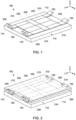
FIG. 1 is an oblique view of an integrated circuit package, according to an embodiment of the present description. -
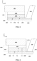
FIG. 2 is an oblique view of the integrated circuit package ofFIG. 1 having a heat dissipation device thermally coupled thereto, according to an embodiment of the present description. -
FIGs. 3-5 are side cross-sectional views of electronic assemblies including a heat dissipation device thermally coupled to a photonic integrated circuit device with a thermal interface structure, according to embodiments of the present description. -
FIG. 6 is a side cross-sectional view of a thermal interface structure attached to a heat dissipation structure, according to an embodiment of the present description. -
FIG. 7 is a side cross-sectional view of a thermal interface structure, according to one embodiment of the present description. -
FIG. 8 is a side cross-sectional view of a silicon photonic integrated circuit device with a cladding material layer disposed thereon, according to an embodiment of the present description. -
FIG. 9 is an electronic system, according to one embodiment of the present description. - In the following detailed description, reference is made to the accompanying drawings that show, by way of illustration, specific embodiments in which the claimed subject matter may be practiced. These embodiments are described in sufficient detail to enable those skilled in the art to practice the subject matter. It is to be understood that the various embodiments, although different, are not necessarily mutually exclusive. For example, a particular feature, structure, or characteristic described herein, in connection with one embodiment, may be implemented within other embodiments without departing from the scope of the claimed subject matter. References within this specification to "one embodiment" or "an embodiment" mean that a particular feature, structure, or characteristic described in connection with the embodiment is included in at least one implementation encompassed within the present description. Therefore, the use of the phrase "one embodiment" or "in an embodiment" does not necessarily refer to the same embodiment. In addition, it is to be understood that the location or arrangement of individual elements within each disclosed embodiment may be modified without departing from the spirit and scope of the claimed subject matter. The following detailed description is, therefore, not to be taken in a limiting sense, and the scope of the subject matter is defined only by the appended claims, appropriately interpreted, along with the full range of equivalents to which the appended claims are entitled. In the drawings, like numerals refer to the same or similar elements or functionality throughout the several views, and that elements depicted therein are not necessarily to scale with one another, rather individual elements may be enlarged or reduced in order to more easily comprehend the elements in the context of the present description.
- The terms "over", "to", "between" and "on" as used herein may refer to a relative position of one layer with respect to other layers. One layer "over" or "on" another layer or bonded "to" another layer may be directly in contact with the other layer or may have one or more intervening layers. One layer "between" layers may be directly in contact with the layers or may have one or more intervening layers.
- The term "package" generally refers to a self-contained carrier of one or more dice, where the dice are attached to the package substrate, and may be encapsulated for protection, with integrated or wire-bonded interconnects between the dice and leads, pins or bumps located on the external portions of the package substrate. The package may contain a single die, or multiple dice, providing a specific function. The package is usually mounted on a printed circuit board for interconnection with other packaged integrated circuits and discrete components, forming a larger circuit.
- Here, the term "cored" generally refers to a substrate of an integrated circuit package built upon a board, card or wafer comprising a non-flexible stiff material. Typically, a small printed circuit board is used as a core, upon which integrated circuit device and discrete passive components may be soldered. Typically, the core has vias extending from one side to the other, allowing circuitry on one side of the core to be coupled directly to circuitry on the opposite side of the core. The core may also serve as a platform for building up layers of conductors and dielectric materials.
- Here, the term "coreless" generally refers to a substrate of an integrated circuit package having no core. The lack of a core allows for higher-density package architectures, as the through-vias have relatively large dimensions and pitch compared to high-density interconnects.
- Here, the term "land side", if used herein, generally refers to the side of the substrate of the integrated circuit package closest to the plane of attachment to a printed circuit board, motherboard, or other package. This is in contrast to the term "die side", which is the side of the substrate of the integrated circuit package to which the die or dice are attached.
- Here, the term "dielectric" generally refers to any number of non-electrically conductive materials that make up the structure of a package substrate. For purposes of this disclosure, dielectric material may be incorporated into an integrated circuit package as layers of laminate film or as a resin molded over integrated circuit dice mounted on the substrate.
- Here, the term "metallization" generally refers to metal layers formed over and through the dielectric material of the package substrate. The metal layers are generally patterned to form metal structures such as traces and bond pads. The metallization of a package substrate may be confined to a single layer or in multiple layers separated by layers of dielectric.
- Here, the term "bond pad" generally refers to metallization structures that terminate integrated traces and vias in integrated circuit packages and dies. The term "solder pad" may be occasionally substituted for "bond pad" and carries the same meaning.
- Here, the term "solder bump" generally refers to a solder layer formed on a bond pad. The solder layer typically has a round shape, hence the term "solder bump".
- Here, the term "substrate" generally refers to a planar platform comprising dielectric and metallization structures. The substrate mechanically supports and electrically couples one or more IC dies on a single platform, with encapsulation of the one or more IC dies by a moldable dielectric material. The substrate generally comprises solder bumps as bonding interconnects on both sides. One side of the substrate, generally referred to as the "die side", comprises solder bumps for chip or die bonding. The opposite side of the substrate, generally referred to as the "land side", comprises solder bumps for bonding the package to a printed circuit board.
- Here, the term "assembly" generally refers to a grouping of parts into a single functional unit. The parts may be separate and are mechanically assembled into a functional unit, where the parts may be removable. In another instance, the parts may be permanently bonded together. In some instances, the parts are integrated together.
- Throughout the specification, and in the claims, the term "connected" means a direct connection, such as electrical, mechanical, or magnetic connection between the things that are connected, without any intermediary devices.
- The term "coupled" means a direct or indirect connection, such as a direct electrical, mechanical, magnetic or fluidic connection between the things that are connected or an indirect connection, through one or more passive or active intermediary devices.
- The term "circuit" or "module" may refer to one or more passive and/or active components that are arranged to cooperate with one another to provide a desired function. The term "signal" may refer to at least one current signal, voltage signal, magnetic signal, or data/clock signal. The meaning of "a," "an," and "the" include plural references. The meaning of "in" includes "in" and "on."
- The vertical orientation is in the z-direction and it is understood that recitations of "top", "bottom", "above" and "below" refer to relative positions in the z-dimension with the usual meaning. However, it is understood that embodiments are not necessarily limited to the orientations or configurations illustrated in the figure.
- The terms "substantially," "close," "approximately," "near," and "about," generally refer to being within +/- 10% of a target value (unless specifically specified). Unless otherwise specified the use of the ordinal adjectives "first," "second," and "third," etc., to describe a common object, merely indicate that different instances of like objects to which are being referred and are not intended to imply that the objects so described must be in a given sequence, either temporally, spatially, in ranking or in any other manner.
- For the purposes of the present disclosure, phrases "A and/or B" and "A or B" mean (A), (B), or (A and B). For the purposes of the present disclosure, the phrase "A, B, and/or C" means (A), (B), (C), (A and B), (A and C), (B and C), or (A, B and C).
- Views labeled "cross-sectional", "profile" and "plan" correspond to orthogonal planes within a cartesian coordinate system. Thus, cross-sectional and profile views are taken in the x-z plane, and plan views are taken in the x-y plane. Typically, profile views in the x-z plane are cross-sectional views. Where appropriate, drawings are labeled with axes to indicate the orientation of the figure.
- Embodiments of the present description relate to the removal of heat from a silicon photonic integrated circuit device, wherein the removal of heat is facilitated with an optically compatible thermal interface structure thereon. The thermal interface structures may comprise stack-up designs, including an optical isolation structure and a thermal interface material, which reduces light coupling effects, while effectively conducting heat from the silicon photonic integrated circuit device to a heat dissipation device, thereby allowing effective management of the temperature thereof.
-
FIG. 1 illustrates anelectronic assembly 100, such as an integrated circuit package. Theelectronic assembly 100 may include at least one silicon photonic integratedcircuit device 200 electrically attached to apackage substrate 110, wherein each silicon photonic integratedcircuit device 200 may have anoptical communication cable 150, such as an optic fiber cable, attached thereto. Thepackage substrate 110 may be any appropriate structure, including, but not limited to, an interposer. Thepackage substrate 110 may have afirst surface 112, an opposingsecond surface 114, and at least oneside 116 extending between thefirst surface 112 and thesecond surface 114. As illustrated, the silicon photonic integratedcircuit devices 200 may be attached proximate the side(s) 116 of thepackage substrate 110 to allow for easier attachment access for theoptical communication cable 150. - As further shown in
FIG. 1 , a plurality of additionalintegrated circuit devices package substrate 110. Each of the additionalintegrated circuit devices - In one embodiment of the present description, at least one of the
integrated circuit devices package substrate 110 in a configuration generally known as a flip-chip or controlled collapse chip connection ("C4") configuration. In another embodiment of the present description (not shown), the silicon photonic integratedcircuit devices 200 may be electrically attached to thepackage substrate 110 in an "open cavity" configuration, wherein the silicon photonic integratedcircuit devices 200 are at least partially embedded in thepackage substrate 110 that allows for direct attachment of the silicon photonic integratedcircuit devices 200 to electronic integrated chips 210 (a controller for the silicon photonic integrated circuit devices 200) for better power efficiency and allows for less obstructed access to the silicon photonic integrated circuit device for the attachment of theoptical communication cables 150. - The
package substrate 110 may comprise a plurality of dielectric material layers (not shown), which may include build-up films and/or solder resist layers, and may be composed of an appropriate dielectric material, including, but not limited to, bismaleimide triazine resin, fire retardant grade 4 material, polyimide material, silica filled epoxy material, glass reinforced epoxy material, low temperature co-fired ceramic materials, and the like, as well as low-k and ultra low-k dielectrics (dielectric constants less than about 3.6), including, but not limited to, carbon doped dielectrics, fluorine doped dielectrics, porous dielectrics, organic polymeric dielectrics, fluoropolymers, and the like. - The
package substrate 110 may further include conductive routes or "metallization" (not shown) extending through thepackage substrate 110 for the interconnection of theintegrated circuit devices package substrate 110 to an external board (not shown). These conductive routes (not shown) may be a combination of conductive traces (not shown) formed between the dielectric material layers (not shown) and conductive vias (not shown) extending through the dielectric material layers (not shown). The structure and fabrication of conductive traces and conductive vias are well known in the art and are not shown or described for purposes of clarity and conciseness. The conductive traces and the conductive vias may be made of any appropriate electrically conductive material, including, but not limited to, metals, such as copper, silver, nickel, gold, and aluminum, alloys thereof, and the like. As will be understood to those skilled in the art, thepackage substrate 110 may be a cored substrate or a coreless substrate. - As shown in
FIG. 2 , thepackage substrate 110 may include aheat dissipation device 300 disposed thereon, wherein theheat dissipation device 300 may be thermally coupled to theintegrated circuit devices integrated circuit devices heat dissipation device 300 with standard thermal interface materials with a high loading of thermally conductive filler materials, such as metal and/or ceramic particles. However, as also previously discussed, such thermal interface materials may not be compatible with the silicon photonic integratedcircuit devices 200. The embodiments of the present description are directed to thermal interface structures for these photonicintegrated circuit devices 200. - The
heat dissipation device 300 may comprise any appropriate thermally conductive structure, including but not limited to an integrated heat spreader, a heat sink, a heat pipe, a thermoelectric cooler, a cold plate, and the like, and may be made of any appropriate thermally conductive material, including, but not limited to, metals, such as copper, silver, nickel, gold, and aluminum, alloys thereof, and the like. In one embodiment of the present description, theheat dissipation device 300 may include a cut-out window or notch therein to allow for a less obstructed access to the silicon photonic integrated circuit device for the attachment of theoptical communication cables 150. -
FIGs. 3-8 illustrate side cross-sectional views of embodiments of the present description. It is noted that various processes and techniques for the electrical attachment of a photonic integrated circuit device to a package substrate is well known in the art and, thus, for the sake of clarity and conciseness will not be discussed nor will the package substrate be illustrated. - As shown in
FIG. 3 , the silicon photonic integratedcircuit device 200 may be formed having afirst surface 202 and an opposingsecond surface 204. As will be understood to those skilled in the art, thefirst surface 202 may contain active circuitry (not shown), active structures (not shown), communication structures (not shown - such as waveguides, grating couplers, and the like), interconnection structures (not shown - such as bond pads, and structures (not shown - e.g., sockets, clips, plugs and the like) for connection of theoptical communication cable 150. In one embodiment of the present description, the entire silicon photonic integratedcircuit device 200 may be thinned, such as by etching, to a thickness T1 of between about 10 and 20 microns. Athermal interface structure 400 may then be formed on the silicon photonic integratedcircuit device 200. Thethermal interface structure 400 may comprise an optical isolation structure, such as a light insulating die attachfilm 410, asilicon heat spreader 420, and a thermalinterface material layer 430. The light insulating die attachfilm 410 may be formed abutting thefirst surface 202 of the silicon photonic integratedcircuit device 200. The light insulating die attachfilm 410 may be any appropriate adhesive which does not significantly absorb, scatter, and/or couple light (photons) from the communication structures on thefirst surface 202. In one embodiment, the light insulating die attachfilm 410 may include, but is not limited to, silicones, acrylates, epoxies, rubbers, fused silicas, acrylics, and the like. The light insulating die attachfilm 410 includes silica filler particles. When the refraction index of the light insulating die attachfilm 410 substantially matches the refraction index of the silica filler particles, the light insulating die attachfilm 410 is substantially optically transparent. - In one embodiment of the present description, the light insulating die attach
film 410 may have a thickness T2 of between about 5 and 20 microns, but not limited thereto. The rule of thumb is that the minimum thickness T2 needs to be at least two times larger than the mode field diameter of communication structures on thefirst surface 202 in order to effectively insulate light. As will be understood to those skilled in the art, the maximum thickness T2 of the light insulation die attachfilm 410 will depend on desired parameter goals. For example, as the thermal conductivity of die attach films are typically relatively low (e.g., between about 0.2 and 0.4 watts per meter*Kelvin), a thinner film closer to 5 microns may result in a lower thermal resistance and may be preferred in most cases for more efficient heat removal. However, in order to accommodate larger packages and potential warpage, a thicker film of closer to 20 microns may be chosen to accommodate such warpage. - The
silicon heat spreader 420 may contact the light insulating die attachfilm 410 to adhere it to the silicon photonic integratedcircuit device 200 for improved heat removal. As the light insulating die attachfilm 410 optically isolates thefirst surface 202 of the silicon photonic integratedcircuit device 200, thesilicon heat spreader 420 will not cause light absorption, scattering, and/or coupling. Furthermore, thesilicon heat spreader 420 will have substantially the same coefficient of thermal expansion as the silicon photonic integratedcircuit device 200 to minimize thermally induced mechanical stresses that could damage components of the silicon photonic integratedcircuit device 200. - The thermal
interface material layer 430 may be disposed between thesilicon heat spreader 420 and theheat dissipation device 300 for thermal coupling therebetween. As the thermalinterface material layer 430 is between thesilicon heat spreader 420 and theheat dissipation device 300, and does not contact the silicon photonic integrated circuit device, the thermalinterface material layer 430 may be any appropriate thermally conductive material, filled or unfilled. - As will be understood, before the assembly of the electronic assembly 100 (see
FIG. 2 ), the light insulative die attachfilm 410 may be pre-attached to thesilicon heat spreader 420 for easier handling. As will be further understood, the thermalinterface material layer 430 may be pre-attached toheat dissipation device 300 to eliminate a step of pick and place. - As shown in
FIG. 4 , in one embodiment of the present description, athermal interface structure 500 may comprise an optical isolation structure, such as anair gap 270 formed in asilicon plateau 510 of the silicon photonic integratedcircuit device 200, and a thermal interface material, such as a compliantthermal interface pad 520. In an embodiment of the present description, the silicon photonic integratedcircuit device 200 may be thinned by selective etching to form thefirst surface 202, such that the at least onesilicon plateau 510 extends from thefirst surface 202. The selective etching forms theair gap 270 within thesilicon plateau 510 in at least onearea 260 where at least one waveguide is formed, and removes silicon in at least onearea 250 where a grating coupler is formed (i.e., area for the attachment of the optical communication cable 150), which results in the formation of the at least onesilicon plateau 510. In one embodiment of the present description, thesilicon plateau 510 may have a thickness T3 of between about 100 and 200 microns for heat spreading. Theair gap 270 in at least one area 260 (where at least one waveguide is formed) prevents light absorption, scattering, and/or coupling, as will be understood to those skilled in the art. - In an embodiment of the present description, the compliant
thermal interface pad 520 may be disposed between thesilicon plateau 510 of the silicon photonic integratedcircuit device 200 and theheat dissipation device 300. In one embodiment, the compliantthermal interface pad 520 is sufficiently conformable, resilient, and/or deformable is to reduce loading stress from theheat dissipation device 300 to the silicon photonic integratedcircuit device 200, which may damage components within the silicon photonic integratedcircuit device 200 or even crack the silicon photonic integratedcircuit device 200 itself. Furthermore, in an embodiment of the present description, the compliantthermal interface pad 520 may be sufficiently rigid to prevent it from extending too far into theair gap 270 over thewaveguide area 260. It is understood that the compliantthermal interface pad 520 may partially extend into theair gap 270, as long as there is a distance of two times the "mode field diameter (MFD)" between thefirst surface 202 over thewaveguide area 260 and thethermal interface pad 520. In one embodiment, the compliantthermal interface pad 520 may include, but is not limited to, gap filler material (such as silicone rubber carrier material containing thermally conductive ceramic filler particles), thermally conductive elastomer, vertical carbon thermal interface material, and the like. - In an embodiment of the present description, as shown in
FIG. 5 , athermal interface structure 600 may be formed between the silicon photonic integratedcircuit device 200 and theheat dissipation device 300. Thethermal interface structure 600 may comprise an optical isolation structure, such as acladding material layer 610, and a thermal interface material layer, such as athermal interface tape 620. Thecladding material layer 610 may be formed abutting thefirst surface 202 of the silicon photonic integratedcircuit device 200. Thecladding material layer 610 may be any appropriate material which does not significantly absorb, scatter, and/or couple light (photons). Thecladding material layer 610 includes silicones, acrylates, epoxies or acrylics. In one embodiment of the present description, thecladding material layer 610 may be substantially transparent. In another embodiment of the present description, thecladding material layer 610 may have a refraction index between about 1.3 and 1.5. In a further embodiment of the present description, thecladding material layer 610 may have a thickness T4 of between about 2 and 3 times the mode field diameter of connection structures, such as waveguides, within the silicon photonic integratedcircuit device 200. - In one embodiment of the present description, the
thermal interface tape 620 may include, but is not limited to, gap filler material (such as silicone rubber carrier material containing thermally conductive ceramic filler particles), thermally conductive elastomer, vertical carbon thermal interface material, and the like. In another embodiment of the present description, thethermal interface tape 620 can be replaced by thermal grease or a polymer thermal interface material. - As will be understood, the
thermal interface structure 600 may be pre-attached to theheat dissipation device 300 for easier handling, as shown inFIG. 6 . As will be further understood, the thermal interface structure, i.e., the combination of thecladding material layer 610 and thethermal interface tape 620 may be supplied as a stand-alone product, as shown inFIG. 7 . As will be further understood, thecladding material layer 610 may be pre-attached to the silicon photonic integratedcircuit device 200, as shown inFIG. 8 . -
FIG. 9 illustrates an electronic orcomputing device 700 in accordance with one implementation of the present description. Thecomputing device 700 may include a housing 701 having aboard 702 disposed therein. Thecomputing device 700 may include a number of integrated circuit components, including but not limited to aprocessor 704, at least onecommunication chip flash memory 712, a graphics processor orCPU 714, a digital signal processor (not shown), a crypto processor (not shown), achipset 716, an antenna, a display (touchscreen display), a touchscreen controller, a battery, an audio codec (not shown), a video codec (not shown), a power amplifier (AMP), a global positioning system (GPS) device, a compass, an accelerometer (not shown), a gyroscope (not shown), a speaker, a camera, and a mass storage device (not shown) (such as hard disk drive, compact disk (CD), digital versatile disk (DVD), and so forth). Any of the integrated circuit components may be physically and electrically coupled to theboard 702. In some implementations, at least one of the integrated circuit components may be a part of theprocessor 704. - The communication chip enables wireless communications for the transfer of data to and from the computing device. The term "wireless" and its derivatives may be used to describe circuits, devices, systems, methods, techniques, communications channels, etc., that may communicate data through the use of modulated electromagnetic radiation through a non-solid medium. The term does not imply that the associated devices do not contain any wires, although in some embodiments they might not. The communication chip may implement any of a number of wireless standards or protocols, including but not limited to Wi-Fi (IEEE 802.11 family), WiMAX (IEEE 802.16 family), IEEE 802.20, long term evolution (LTE), Ev-DO, HSPA+, HSDPA+, HSUPA+, EDGE, GSM, GPRS, CDMA, TDMA, DECT, Bluetooth, derivatives thereof, as well as any other wireless protocols that are designated as 3G, 4G, 5G, and beyond. The computing device may include a plurality of communication chips. For instance, a first communication chip may be dedicated to shorter range wireless communications such as Wi-Fi and Bluetooth and a second communication chip may be dedicated to longer range wireless communications such as GPS, EDGE, GPRS, CDMA, WiMAX, LTE, Ev-DO, and others.
- The term "processor" may refer to any device or portion of a device that processes electronic data from registers and/or memory to transform that electronic data into other electronic data that may be stored in registers and/or memory.
- At least one of the integrated circuit components may include an integrated circuit package, which comprises a package substrate, wherein the package substrate includes a first surface; a heat dissipation structure within the package substrate; and a photonic integrated circuit device, wherein the silicon photonic integrated circuit device is attached adjacent to the first surface of the package substrate and thermally coupled to the heat dissipation structure.
- In various implementations, the computing device may be a laptop, a netbook, a notebook, an ultrabook, a smartphone, a tablet, a personal digital assistant (PDA), an ultra-mobile PC, a mobile phone, a desktop computer, a server, a printer, a scanner, a monitor, a set-top box, an entertainment control unit, a digital camera, a portable music player, or a digital video recorder. In further implementations, the computing device may be any other electronic device that processes data.
- It is understood that the subject matter of the present description is not necessarily limited to specific applications illustrated in
FIGs. 1-9 . The subject matter may be applied to other integrated circuit devices and assembly applications, as well as any appropriate electronic application, as will be understood to those skilled in the art. - Having thus described in detail embodiments of the present invention, it is understood that the invention defined by the appended claims is not to be limited by particular details set forth in the above description, as many apparent variations thereof are possible without departing from the scope of the invention as defined by the claims.
Claims (8)
- An apparatus, comprising:a photonic integrated circuit device (200), wherein the photonic integrated circuit device (200) has a first surface;an optical isolation structure proximate the first surface of the photonic integrated circuit device (200);a thermal interface material (430) on the optical isolation structure; anda heat dissipation device (300), wherein the heat dissipation device (300) is thermally coupled to the thermal interface material (430), characterized in thatthe optical isolation structure comprises a light insulating die attach film (410) selected from the group consisting of silicones, acrylates, epoxies, rubbers, fused silicas, and acrylics, or a cladding material layer selected form the group consisting of silicones, acrylates, epoxies, and acrylics, in thatthe light insulating die attach film (410) comprises silica filler particles and has a refraction index substantially matching the refraction index of the silica filler particles, or in thatthe optical isolation structure comprises an air gap formed in the photonic integrated circuit device (200).
- The apparatus of claim 1, wherein the light insulation die attach film (410) contains no filler materials.
- The apparatus of any of claims 1 or 2, further comprising a heat spreader (420) between the light insulation die attach film (410) and the thermal interface material (430).
- The apparatus of claim 1, wherein the air gap is formed in a plateau formed in the photonic integrated circuit device (200).
- The apparatus of any of claims 1 to 4, wherein the thermal interface material (430) comprises a compliant thermal interface pad that is selected from the group consisting of gap filler material, thermally conductive elastomer, and vertical carbon thermal interface material (430).
- The apparatus of claim 5, wherein the thermal interface material (430) comprises a thermal interface tape selected from the group consisting of gap filler material, thermally conductive elastomer, and vertical carbon thermal interface material (430).
- The apparatus of any of claims 1 to 6, further comprising:
a package substrate (110), wherein the package substrate (110) includes a first surface, wherein the photonic integrated circuit device (200) is electrically attached to the package substrate (110). - The apparatus of claim 7, further comprising:
an electronic board, wherein the integrated circuit package is electrically attached to the electronic board.
Applications Claiming Priority (1)
| Application Number | Priority Date | Filing Date | Title |
|---|---|---|---|
| US17/338,928 US20220390694A1 (en) | 2021-06-04 | 2021-06-04 | Thermal interface structures for optical communication devices |
Publications (2)
| Publication Number | Publication Date |
|---|---|
| EP4099070A1 EP4099070A1 (en) | 2022-12-07 |
| EP4099070B1 true EP4099070B1 (en) | 2025-06-18 |
Family
ID=80786762
Family Applications (1)
| Application Number | Title | Priority Date | Filing Date |
|---|---|---|---|
| EP22158792.6A Active EP4099070B1 (en) | 2021-06-04 | 2022-02-25 | Thermal interface structures for optical communication devices |
Country Status (2)
| Country | Link |
|---|---|
| US (1) | US20220390694A1 (en) |
| EP (1) | EP4099070B1 (en) |
Families Citing this family (2)
| Publication number | Priority date | Publication date | Assignee | Title |
|---|---|---|---|---|
| GB2625806A (en) * | 2022-12-23 | 2024-07-03 | Light Trace Photonics Ltd | Housing for accommodating a photonic integrated circuit chip |
| EP4720736A1 (en) * | 2024-07-16 | 2026-04-08 | Celestial AI Inc. | Co-packaged optics with optically transparent molding compound |
Family Cites Families (13)
| Publication number | Priority date | Publication date | Assignee | Title |
|---|---|---|---|---|
| CN1182484A (en) * | 1995-04-18 | 1998-05-20 | 阿克佐诺贝尔公司 | Fast switching asymmetric thermo-optical device |
| US20020018636A1 (en) * | 2000-08-02 | 2002-02-14 | Gemfire Corporation | Device and method for variable attenuation of an optical channel |
| JP4004047B2 (en) * | 2003-03-25 | 2007-11-07 | 住友ベークライト株式会社 | Die attach film with dicing sheet function, semiconductor device manufacturing method using the same, and semiconductor device |
| EP1994434A2 (en) * | 2006-03-03 | 2008-11-26 | Gemfire Corporation | Dynamically tunable waveguide chip for optical transforms |
| US8213751B1 (en) * | 2008-11-26 | 2012-07-03 | Optonet Inc. | Electronic-integration compatible photonic integrated circuit and method for fabricating electronic-integration compatible photonic integrated circuit |
| WO2012069929A1 (en) * | 2010-11-25 | 2012-05-31 | Fci | Optical circuit board |
| US9673131B2 (en) * | 2013-04-09 | 2017-06-06 | Intel Corporation | Integrated circuit package assemblies including a glass solder mask layer |
| US10242976B2 (en) * | 2016-12-31 | 2019-03-26 | Intel Corporation | In-package photonics integration and assembly architecture |
| JP6811664B2 (en) * | 2017-03-24 | 2021-01-13 | ルネサスエレクトロニクス株式会社 | Semiconductor devices and their manufacturing methods |
| US11259399B2 (en) * | 2018-02-21 | 2022-02-22 | Intel Corporation | Socket with thermal conductor |
| US20200126887A1 (en) * | 2018-10-18 | 2020-04-23 | Intel Corporation | Thin line dam on underfill material to contain thermal interface materials |
| JP2020134599A (en) * | 2019-02-14 | 2020-08-31 | 古河電気工業株式会社 | Optical semiconductor devices and integrated semiconductor lasers |
| US12085769B2 (en) * | 2021-04-23 | 2024-09-10 | Taiwan Semiconductor Manufacturing Company, Ltd. | Integrated circuit device and method |
-
2021
- 2021-06-04 US US17/338,928 patent/US20220390694A1/en not_active Abandoned
-
2022
- 2022-02-25 EP EP22158792.6A patent/EP4099070B1/en active Active
Also Published As
| Publication number | Publication date |
|---|---|
| US20220390694A1 (en) | 2022-12-08 |
| EP4099070A1 (en) | 2022-12-07 |
Similar Documents
| Publication | Publication Date | Title |
|---|---|---|
| US12366713B2 (en) | Heat dissipation structures for optical communication devices | |
| US11933555B2 (en) | Heat dissipation device having anisotropic thermally conductive sections and isotropic thermally conductive sections | |
| US10845552B2 (en) | Coreless package architecture for multi-chip opto-electronics | |
| US10943851B1 (en) | Reconstituted wafer assembly | |
| CN107924914B (en) | Platform with Thermally Stable Wireless Interconnect | |
| US11302599B2 (en) | Heat dissipation device having a thermally conductive structure and a thermal isolation structure in the thermally conductive structure | |
| US20240088047A1 (en) | Scalable high speed high bandwidth io signaling package architecture and method of making | |
| EP3840037A1 (en) | Package wrap-around heat spreader | |
| US11652020B2 (en) | Thermal solutions for multi-package assemblies and methods for fabricating the same | |
| EP4099070A1 (en) | Thermal interface structures for optical communication devices | |
| US20210249322A1 (en) | Barrier structures for underfill containment | |
| EP4024446A1 (en) | Heat extraction path from a laser die using a highly conductive thermal interface material in an optical transceiver | |
| US11842826B2 (en) | Additive manufacturing for integrated circuit assembly connector support structures | |
| US12313890B2 (en) | Through-substrate optical vias | |
| US20220413236A1 (en) | Photonic integrated circuit cooling with a thermal die | |
| US20230318247A1 (en) | Package with multiple photonic integrated circuit dies optically coupled with each other | |
| US12165994B2 (en) | Radio frequency antennas and waveguides for communication between integrated circuit devices | |
| US11887944B2 (en) | Additive manufacturing for integrated circuit assembly connectors | |
| US20230163047A1 (en) | Fluid conduit within a package substrate for two-phase immersion cooling systems | |
| US20220404553A1 (en) | Optical communication between integrated circuit device assemblies | |
| US11895815B2 (en) | Additive manufacturing for integrated circuit assembly cables | |
| US20250309030A1 (en) | Microelectronic structures including ihs coupling enhancement structures for thermal degradation mitigation | |
| US20240194657A1 (en) | Integrated photonic device and electronic device architectures | |
| WO2010131578A1 (en) | Semiconductor device with built-in optical signal input and output device and electronic device equipped with same | |
| JP2006128315A (en) | Semiconductor device heat dissipation structure and heat dissipation method, and electronic equipment using the same |
Legal Events
| Date | Code | Title | Description |
|---|---|---|---|
| PUAI | Public reference made under article 153(3) epc to a published international application that has entered the european phase |
Free format text: ORIGINAL CODE: 0009012 |
|
| STAA | Information on the status of an ep patent application or granted ep patent |
Free format text: STATUS: THE APPLICATION HAS BEEN PUBLISHED |
|
| AK | Designated contracting states |
Kind code of ref document: A1 Designated state(s): AL AT BE BG CH CY CZ DE DK EE ES FI FR GB GR HR HU IE IS IT LI LT LU LV MC MK MT NL NO PL PT RO RS SE SI SK SM TR |
|
| STAA | Information on the status of an ep patent application or granted ep patent |
Free format text: STATUS: REQUEST FOR EXAMINATION WAS MADE |
|
| 17P | Request for examination filed |
Effective date: 20230531 |
|
| RBV | Designated contracting states (corrected) |
Designated state(s): AL AT BE BG CH CY CZ DE DK EE ES FI FR GB GR HR HU IE IS IT LI LT LU LV MC MK MT NL NO PL PT RO RS SE SI SK SM TR |
|
| GRAP | Despatch of communication of intention to grant a patent |
Free format text: ORIGINAL CODE: EPIDOSNIGR1 |
|
| STAA | Information on the status of an ep patent application or granted ep patent |
Free format text: STATUS: GRANT OF PATENT IS INTENDED |
|
| INTG | Intention to grant announced |
Effective date: 20250207 |
|
| GRAS | Grant fee paid |
Free format text: ORIGINAL CODE: EPIDOSNIGR3 |
|
| GRAA | (expected) grant |
Free format text: ORIGINAL CODE: 0009210 |
|
| STAA | Information on the status of an ep patent application or granted ep patent |
Free format text: STATUS: THE PATENT HAS BEEN GRANTED |
|
| AK | Designated contracting states |
Kind code of ref document: B1 Designated state(s): AL AT BE BG CH CY CZ DE DK EE ES FI FR GB GR HR HU IE IS IT LI LT LU LV MC MK MT NL NO PL PT RO RS SE SI SK SM TR |
|
| REG | Reference to a national code |
Ref country code: GB Ref legal event code: FG4D |
|
| REG | Reference to a national code |
Ref country code: CH Ref legal event code: EP |
|
| REG | Reference to a national code |
Ref country code: DE Ref legal event code: R096 Ref document number: 602022015964 Country of ref document: DE |
|
| REG | Reference to a national code |
Ref country code: CH Ref legal event code: EP |
|
| P01 | Opt-out of the competence of the unified patent court (upc) registered |
Free format text: CASE NUMBER: APP_26684/2025 Effective date: 20250605 |
|
| REG | Reference to a national code |
Ref country code: IE Ref legal event code: FG4D |
|
| REG | Reference to a national code |
Ref country code: NL Ref legal event code: FP |
|
| PG25 | Lapsed in a contracting state [announced via postgrant information from national office to epo] |
Ref country code: FI Free format text: LAPSE BECAUSE OF FAILURE TO SUBMIT A TRANSLATION OF THE DESCRIPTION OR TO PAY THE FEE WITHIN THE PRESCRIBED TIME-LIMIT Effective date: 20250618 |
|
| REG | Reference to a national code |
Ref country code: LT Ref legal event code: MG9D |
|
| PG25 | Lapsed in a contracting state [announced via postgrant information from national office to epo] |
Ref country code: GR Free format text: LAPSE BECAUSE OF FAILURE TO SUBMIT A TRANSLATION OF THE DESCRIPTION OR TO PAY THE FEE WITHIN THE PRESCRIBED TIME-LIMIT Effective date: 20250919 Ref country code: NO Free format text: LAPSE BECAUSE OF FAILURE TO SUBMIT A TRANSLATION OF THE DESCRIPTION OR TO PAY THE FEE WITHIN THE PRESCRIBED TIME-LIMIT Effective date: 20250918 |
|
| PG25 | Lapsed in a contracting state [announced via postgrant information from national office to epo] |
Ref country code: BG Free format text: LAPSE BECAUSE OF FAILURE TO SUBMIT A TRANSLATION OF THE DESCRIPTION OR TO PAY THE FEE WITHIN THE PRESCRIBED TIME-LIMIT Effective date: 20250618 |
|
| PG25 | Lapsed in a contracting state [announced via postgrant information from national office to epo] |
Ref country code: HR Free format text: LAPSE BECAUSE OF FAILURE TO SUBMIT A TRANSLATION OF THE DESCRIPTION OR TO PAY THE FEE WITHIN THE PRESCRIBED TIME-LIMIT Effective date: 20250618 |
|
| PG25 | Lapsed in a contracting state [announced via postgrant information from national office to epo] |
Ref country code: RS Free format text: LAPSE BECAUSE OF FAILURE TO SUBMIT A TRANSLATION OF THE DESCRIPTION OR TO PAY THE FEE WITHIN THE PRESCRIBED TIME-LIMIT Effective date: 20250918 |
|
| PG25 | Lapsed in a contracting state [announced via postgrant information from national office to epo] |
Ref country code: LV Free format text: LAPSE BECAUSE OF FAILURE TO SUBMIT A TRANSLATION OF THE DESCRIPTION OR TO PAY THE FEE WITHIN THE PRESCRIBED TIME-LIMIT Effective date: 20250618 |
|
| PG25 | Lapsed in a contracting state [announced via postgrant information from national office to epo] |
Ref country code: PT Free format text: LAPSE BECAUSE OF FAILURE TO SUBMIT A TRANSLATION OF THE DESCRIPTION OR TO PAY THE FEE WITHIN THE PRESCRIBED TIME-LIMIT Effective date: 20251020 |
|
| REG | Reference to a national code |
Ref country code: AT Ref legal event code: MK05 Ref document number: 1804699 Country of ref document: AT Kind code of ref document: T Effective date: 20250618 |
|
| PG25 | Lapsed in a contracting state [announced via postgrant information from national office to epo] |
Ref country code: IS Free format text: LAPSE BECAUSE OF FAILURE TO SUBMIT A TRANSLATION OF THE DESCRIPTION OR TO PAY THE FEE WITHIN THE PRESCRIBED TIME-LIMIT Effective date: 20251018 |
|
| PG25 | Lapsed in a contracting state [announced via postgrant information from national office to epo] |
Ref country code: AT Free format text: LAPSE BECAUSE OF FAILURE TO SUBMIT A TRANSLATION OF THE DESCRIPTION OR TO PAY THE FEE WITHIN THE PRESCRIBED TIME-LIMIT Effective date: 20250618 Ref country code: SM Free format text: LAPSE BECAUSE OF FAILURE TO SUBMIT A TRANSLATION OF THE DESCRIPTION OR TO PAY THE FEE WITHIN THE PRESCRIBED TIME-LIMIT Effective date: 20250618 |
|
| PG25 | Lapsed in a contracting state [announced via postgrant information from national office to epo] |
Ref country code: CZ Free format text: LAPSE BECAUSE OF FAILURE TO SUBMIT A TRANSLATION OF THE DESCRIPTION OR TO PAY THE FEE WITHIN THE PRESCRIBED TIME-LIMIT Effective date: 20250618 |
|
| PG25 | Lapsed in a contracting state [announced via postgrant information from national office to epo] |
Ref country code: PL Free format text: LAPSE BECAUSE OF FAILURE TO SUBMIT A TRANSLATION OF THE DESCRIPTION OR TO PAY THE FEE WITHIN THE PRESCRIBED TIME-LIMIT Effective date: 20250618 |
|
| PG25 | Lapsed in a contracting state [announced via postgrant information from national office to epo] |
Ref country code: EE Free format text: LAPSE BECAUSE OF FAILURE TO SUBMIT A TRANSLATION OF THE DESCRIPTION OR TO PAY THE FEE WITHIN THE PRESCRIBED TIME-LIMIT Effective date: 20250618 |
|
| PG25 | Lapsed in a contracting state [announced via postgrant information from national office to epo] |
Ref country code: SK Free format text: LAPSE BECAUSE OF FAILURE TO SUBMIT A TRANSLATION OF THE DESCRIPTION OR TO PAY THE FEE WITHIN THE PRESCRIBED TIME-LIMIT Effective date: 20250618 |
|
| PG25 | Lapsed in a contracting state [announced via postgrant information from national office to epo] |
Ref country code: ES Free format text: LAPSE BECAUSE OF FAILURE TO SUBMIT A TRANSLATION OF THE DESCRIPTION OR TO PAY THE FEE WITHIN THE PRESCRIBED TIME-LIMIT Effective date: 20250618 |
|
| PGFP | Annual fee paid to national office [announced via postgrant information from national office to epo] |
Ref country code: NL Payment date: 20260128 Year of fee payment: 5 |
|
| REG | Reference to a national code |
Ref country code: DE Ref legal event code: R097 Ref document number: 602022015964 Country of ref document: DE |
|
| PGFP | Annual fee paid to national office [announced via postgrant information from national office to epo] |
Ref country code: GB Payment date: 20260128 Year of fee payment: 5 |
|
| PG25 | Lapsed in a contracting state [announced via postgrant information from national office to epo] |
Ref country code: DK Free format text: LAPSE BECAUSE OF FAILURE TO SUBMIT A TRANSLATION OF THE DESCRIPTION OR TO PAY THE FEE WITHIN THE PRESCRIBED TIME-LIMIT Effective date: 20250618 |
|
| PGFP | Annual fee paid to national office [announced via postgrant information from national office to epo] |
Ref country code: DE Payment date: 20260102 Year of fee payment: 5 |
|
| PG25 | Lapsed in a contracting state [announced via postgrant information from national office to epo] |
Ref country code: IT Free format text: LAPSE BECAUSE OF FAILURE TO SUBMIT A TRANSLATION OF THE DESCRIPTION OR TO PAY THE FEE WITHIN THE PRESCRIBED TIME-LIMIT Effective date: 20250618 |
|
| PGFP | Annual fee paid to national office [announced via postgrant information from national office to epo] |
Ref country code: FR Payment date: 20260121 Year of fee payment: 5 |
|
| PLBE | No opposition filed within time limit |
Free format text: ORIGINAL CODE: 0009261 |
|
| STAA | Information on the status of an ep patent application or granted ep patent |
Free format text: STATUS: NO OPPOSITION FILED WITHIN TIME LIMIT |
|
| REG | Reference to a national code |
Ref country code: CH Ref legal event code: L10 Free format text: ST27 STATUS EVENT CODE: U-0-0-L10-L00 (AS PROVIDED BY THE NATIONAL OFFICE) Effective date: 20260430 |