EP4095888B1 - Semiconductor device having a reduced concentration of carbon vacancies and method for manufacturing a semiconductor device - Google Patents
Semiconductor device having a reduced concentration of carbon vacancies and method for manufacturing a semiconductor device Download PDFInfo
- Publication number
- EP4095888B1 EP4095888B1 EP21176547.4A EP21176547A EP4095888B1 EP 4095888 B1 EP4095888 B1 EP 4095888B1 EP 21176547 A EP21176547 A EP 21176547A EP 4095888 B1 EP4095888 B1 EP 4095888B1
- Authority
- EP
- European Patent Office
- Prior art keywords
- epitaxial layer
- semiconductor
- carbon
- semiconductor device
- implantation
- Prior art date
- Legal status (The legal status is an assumption and is not a legal conclusion. Google has not performed a legal analysis and makes no representation as to the accuracy of the status listed.)
- Active
Links
Images






Classifications
-
- H—ELECTRICITY
- H10—SEMICONDUCTOR DEVICES; ELECTRIC SOLID-STATE DEVICES NOT OTHERWISE PROVIDED FOR
- H10P—GENERIC PROCESSES OR APPARATUS FOR THE MANUFACTURE OR TREATMENT OF DEVICES COVERED BY CLASS H10
- H10P30/00—Ion implantation into wafers, substrates or parts of devices
- H10P30/20—Ion implantation into wafers, substrates or parts of devices into semiconductor materials, e.g. for doping
- H10P30/222—Ion implantation into wafers, substrates or parts of devices into semiconductor materials, e.g. for doping characterised by the angle between the ion beam and the crystal planes or the main crystal surface
-
- H—ELECTRICITY
- H10—SEMICONDUCTOR DEVICES; ELECTRIC SOLID-STATE DEVICES NOT OTHERWISE PROVIDED FOR
- H10D—INORGANIC ELECTRIC SEMICONDUCTOR DEVICES
- H10D10/00—Bipolar junction transistors [BJT]
- H10D10/40—Vertical BJTs
- H10D10/441—Vertical BJTs having an emitter-base junction ending at a main surface of the body and a base-collector junction ending at a lateral surface of the body
-
- H—ELECTRICITY
- H10—SEMICONDUCTOR DEVICES; ELECTRIC SOLID-STATE DEVICES NOT OTHERWISE PROVIDED FOR
- H10D—INORGANIC ELECTRIC SEMICONDUCTOR DEVICES
- H10D12/00—Bipolar devices controlled by the field effect, e.g. insulated-gate bipolar transistors [IGBT]
- H10D12/01—Manufacture or treatment
- H10D12/031—Manufacture or treatment of IGBTs
-
- H—ELECTRICITY
- H10—SEMICONDUCTOR DEVICES; ELECTRIC SOLID-STATE DEVICES NOT OTHERWISE PROVIDED FOR
- H10D—INORGANIC ELECTRIC SEMICONDUCTOR DEVICES
- H10D12/00—Bipolar devices controlled by the field effect, e.g. insulated-gate bipolar transistors [IGBT]
- H10D12/411—Insulated-gate bipolar transistors [IGBT]
- H10D12/441—Vertical IGBTs
-
- H—ELECTRICITY
- H10—SEMICONDUCTOR DEVICES; ELECTRIC SOLID-STATE DEVICES NOT OTHERWISE PROVIDED FOR
- H10D—INORGANIC ELECTRIC SEMICONDUCTOR DEVICES
- H10D62/00—Semiconductor bodies, or regions thereof, of devices having potential barriers
- H10D62/10—Shapes, relative sizes or dispositions of the regions of the semiconductor bodies; Shapes of the semiconductor bodies
- H10D62/102—Constructional design considerations for preventing surface leakage or controlling electric field concentration
- H10D62/103—Constructional design considerations for preventing surface leakage or controlling electric field concentration for increasing or controlling the breakdown voltage of reverse-biased devices
- H10D62/105—Constructional design considerations for preventing surface leakage or controlling electric field concentration for increasing or controlling the breakdown voltage of reverse-biased devices by having particular doping profiles, shapes or arrangements of PN junctions; by having supplementary regions, e.g. junction termination extension [JTE]
- H10D62/106—Constructional design considerations for preventing surface leakage or controlling electric field concentration for increasing or controlling the breakdown voltage of reverse-biased devices by having particular doping profiles, shapes or arrangements of PN junctions; by having supplementary regions, e.g. junction termination extension [JTE] having supplementary regions doped oppositely to or in rectifying contact with regions of the semiconductor bodies, e.g. guard rings with PN or Schottky junctions
-
- H—ELECTRICITY
- H10—SEMICONDUCTOR DEVICES; ELECTRIC SOLID-STATE DEVICES NOT OTHERWISE PROVIDED FOR
- H10D—INORGANIC ELECTRIC SEMICONDUCTOR DEVICES
- H10D62/00—Semiconductor bodies, or regions thereof, of devices having potential barriers
- H10D62/10—Shapes, relative sizes or dispositions of the regions of the semiconductor bodies; Shapes of the semiconductor bodies
- H10D62/17—Semiconductor regions connected to electrodes not carrying current to be rectified, amplified or switched, e.g. channel regions
- H10D62/177—Base regions of bipolar transistors, e.g. BJTs or IGBTs
-
- H—ELECTRICITY
- H10—SEMICONDUCTOR DEVICES; ELECTRIC SOLID-STATE DEVICES NOT OTHERWISE PROVIDED FOR
- H10D—INORGANIC ELECTRIC SEMICONDUCTOR DEVICES
- H10D62/00—Semiconductor bodies, or regions thereof, of devices having potential barriers
- H10D62/40—Crystalline structures
- H10D62/405—Orientations of crystalline planes
-
- H—ELECTRICITY
- H10—SEMICONDUCTOR DEVICES; ELECTRIC SOLID-STATE DEVICES NOT OTHERWISE PROVIDED FOR
- H10D—INORGANIC ELECTRIC SEMICONDUCTOR DEVICES
- H10D62/00—Semiconductor bodies, or regions thereof, of devices having potential barriers
- H10D62/50—Physical imperfections
- H10D62/53—Physical imperfections the imperfections being within the semiconductor body
-
- H—ELECTRICITY
- H10—SEMICONDUCTOR DEVICES; ELECTRIC SOLID-STATE DEVICES NOT OTHERWISE PROVIDED FOR
- H10D—INORGANIC ELECTRIC SEMICONDUCTOR DEVICES
- H10D62/00—Semiconductor bodies, or regions thereof, of devices having potential barriers
- H10D62/80—Semiconductor bodies, or regions thereof, of devices having potential barriers characterised by the materials
- H10D62/83—Semiconductor bodies, or regions thereof, of devices having potential barriers characterised by the materials being Group IV materials, e.g. B-doped Si or undoped Ge
- H10D62/832—Semiconductor bodies, or regions thereof, of devices having potential barriers characterised by the materials being Group IV materials, e.g. B-doped Si or undoped Ge being Group IV materials comprising two or more elements, e.g. SiGe
- H10D62/8325—Silicon carbide
-
- H—ELECTRICITY
- H10—SEMICONDUCTOR DEVICES; ELECTRIC SOLID-STATE DEVICES NOT OTHERWISE PROVIDED FOR
- H10D—INORGANIC ELECTRIC SEMICONDUCTOR DEVICES
- H10D8/00—Diodes
- H10D8/01—Manufacture or treatment
- H10D8/051—Manufacture or treatment of Schottky diodes
-
- H—ELECTRICITY
- H10—SEMICONDUCTOR DEVICES; ELECTRIC SOLID-STATE DEVICES NOT OTHERWISE PROVIDED FOR
- H10D—INORGANIC ELECTRIC SEMICONDUCTOR DEVICES
- H10D8/00—Diodes
- H10D8/422—PN diodes having the PN junctions in mesas
-
- H—ELECTRICITY
- H10—SEMICONDUCTOR DEVICES; ELECTRIC SOLID-STATE DEVICES NOT OTHERWISE PROVIDED FOR
- H10P—GENERIC PROCESSES OR APPARATUS FOR THE MANUFACTURE OR TREATMENT OF DEVICES COVERED BY CLASS H10
- H10P30/00—Ion implantation into wafers, substrates or parts of devices
- H10P30/20—Ion implantation into wafers, substrates or parts of devices into semiconductor materials, e.g. for doping
- H10P30/202—Ion implantation into wafers, substrates or parts of devices into semiconductor materials, e.g. for doping characterised by the semiconductor materials
- H10P30/204—Ion implantation into wafers, substrates or parts of devices into semiconductor materials, e.g. for doping characterised by the semiconductor materials into Group IV semiconductors
- H10P30/2042—Ion implantation into wafers, substrates or parts of devices into semiconductor materials, e.g. for doping characterised by the semiconductor materials into Group IV semiconductors into crystalline silicon carbide
-
- H—ELECTRICITY
- H10—SEMICONDUCTOR DEVICES; ELECTRIC SOLID-STATE DEVICES NOT OTHERWISE PROVIDED FOR
- H10P—GENERIC PROCESSES OR APPARATUS FOR THE MANUFACTURE OR TREATMENT OF DEVICES COVERED BY CLASS H10
- H10P30/00—Ion implantation into wafers, substrates or parts of devices
- H10P30/20—Ion implantation into wafers, substrates or parts of devices into semiconductor materials, e.g. for doping
- H10P30/21—Ion implantation into wafers, substrates or parts of devices into semiconductor materials, e.g. for doping of electrically active species
-
- H—ELECTRICITY
- H10—SEMICONDUCTOR DEVICES; ELECTRIC SOLID-STATE DEVICES NOT OTHERWISE PROVIDED FOR
- H10P—GENERIC PROCESSES OR APPARATUS FOR THE MANUFACTURE OR TREATMENT OF DEVICES COVERED BY CLASS H10
- H10P30/00—Ion implantation into wafers, substrates or parts of devices
- H10P30/20—Ion implantation into wafers, substrates or parts of devices into semiconductor materials, e.g. for doping
- H10P30/28—Ion implantation into wafers, substrates or parts of devices into semiconductor materials, e.g. for doping characterised by an annealing step, e.g. for activation of dopants
-
- H—ELECTRICITY
- H10—SEMICONDUCTOR DEVICES; ELECTRIC SOLID-STATE DEVICES NOT OTHERWISE PROVIDED FOR
- H10D—INORGANIC ELECTRIC SEMICONDUCTOR DEVICES
- H10D10/00—Bipolar junction transistors [BJT]
-
- H—ELECTRICITY
- H10—SEMICONDUCTOR DEVICES; ELECTRIC SOLID-STATE DEVICES NOT OTHERWISE PROVIDED FOR
- H10D—INORGANIC ELECTRIC SEMICONDUCTOR DEVICES
- H10D12/00—Bipolar devices controlled by the field effect, e.g. insulated-gate bipolar transistors [IGBT]
- H10D12/411—Insulated-gate bipolar transistors [IGBT]
-
- H—ELECTRICITY
- H10—SEMICONDUCTOR DEVICES; ELECTRIC SOLID-STATE DEVICES NOT OTHERWISE PROVIDED FOR
- H10D—INORGANIC ELECTRIC SEMICONDUCTOR DEVICES
- H10D8/00—Diodes
- H10D8/50—PIN diodes
-
- H—ELECTRICITY
- H10—SEMICONDUCTOR DEVICES; ELECTRIC SOLID-STATE DEVICES NOT OTHERWISE PROVIDED FOR
- H10D—INORGANIC ELECTRIC SEMICONDUCTOR DEVICES
- H10D8/00—Diodes
- H10D8/60—Schottky-barrier diodes
Definitions
- the present disclosure relates to semiconductor devices comprising at least one epitaxial layer made from a first semiconductor material comprising carbon, wherein at least one part of the epitaxial layer has a reduced concentration of carbon vacancies with respect to the first semiconductor material of the at least one epitaxial layer as-grown.
- the present disclosure further relates to methods for manufacturing such semiconductor devices.
- US 7 754 589 B2 relates to a method for improving the quality of a SiC layer by effectively reducing or eliminating the carrier trapping centers in the as-grown SiC crystal.
- US2013/183820 A1 discloses a further method to reduce the carbon vacancy concentration in a SiC semiconductor body. That method comprises forming trenches in a SiC body by means of RIE followed by thermal etching, forming a C-rich layer on the sidewalls of said trenches and diffusing them into the semiconductor body by heat treatment.
- US 2014/361312 A1 relates to a SiC reverse blocking MOSFET that includes an active region including a MOS gate structure and a breakdown voltage structure portion surrounding the outer circumference of the active region, which are provided on the surface side of a SiC-n- drift layer that is grown on one main surface of a p+ SiC substrate.
- US 2015/333190 A1 relates to a semiconductor device that includes a semiconductor layer made of a wide bandgap semiconductor, a trench that is selectively formed on a surface portion of the semiconductor layer and that defines a unit cell having a predetermined shape on the surface portion, and a surface electrode that is embedded in the trench so as to cover an upper surface of the unit cell and that forms a Schottky junction between the unit cell and the surface electrode, and side surfaces of the trench are formed of only a plurality of planes that have plane orientations crystallographically equivalent to each other.
- US 2015/108500 A1 discloses a semiconductor device comprising a semiconductor body of a first semiconductor material, wherein at least a part of the semiconductor body constitutes a drift zone of a first conductivity type.
- the semiconductor device further comprises a channel layer structure comprising a semiconductor heterojunction between first and second semiconductor layers electrically coupled to the drift zone.
- the first and second semiconductor layers include semiconductor materials that are different to the first semiconductor material.
- US 9 093 568 B1 discloses that, in a semiconductor diode a semiconductor body includes an injection efficiency control region between a drift region of a first conductivity type and a first electrode region of a second, opposite conductivity type.
- the injection efficiency control region includes a superjunction structure including a barrier region of the first conductivity type and a compensation region of a second conductivity type arranged consecutively along a lateral direction and directly adjoining each other.
- a net dopant concentration of the barrier region averaged along a vertical extension of the barrier region is at least three times greater than a net dopant concentration of the drift region averaged along 20% of a vertical extension of the drift zone adjoining the barrier region.
- Embodiments of the disclosure relate to improved semiconductor devices and methods for their manufacturing. Exemplarily, there is a need for semiconductor devices that have an improved lifetime, low defect density and/or can be manufactured in a flexible way using conventional semiconductor processing steps.
- a semiconductor device comprising at least one epitaxial layer made from a first semiconductor material comprising carbon and having a [0001] crystallographic axis. At least one implantation area is formed at a sidewall of the epitaxial layer, a normal direction of the sidewall being perpendicular to the [0001] crystallographic axis. At least one part of the epitaxial layer has a reduced concentration of carbon vacancies with respect to the first semiconductor material of the at least one epitaxial layer as-grown.
- the at least one at least one epitaxial layer made from a first semiconductor material comprises at least one of n-type 4H-SiC or n-type 6H-SiC semiconductor material.
- the at least one implantation area comprises an implanted species, comprising at least one of carbon ions or silicon ions.
- the at least one part of the epitaxial layer is adjacent to the sidewall and has a concentration of carbon vacancy Z 1/2 of below 10 10 /cm 3 .
- implantation can be performed independent of other processing steps, which are typically performed in parallel to the [0001] crystallographic axis, e.g. on or through the front face of the epitaxial layer.
- motility of an implanted species is improved, which simplifies a later annealing of the at least one epitaxial layer and results in a reduced concentration of carbon vacancies therein.
- the at least one implantation area is formed on one of a plurality of sidewalls of at least one semiconductor chip comprising the at least one epitaxial layer. Implanting a species through a sidewall of a semiconductor chip allows the reduction of carbon vacancies on already separated, almost finished semiconductor circuit component.
- the semiconductor device comprises at least one trench having two sidewalls formed in the at least one epitaxial layer.
- the at least one implantation area is formed on at least one of the two sidewalls of the at least one trench.
- the at least one part of the epitaxial layer corresponds to a sublayer extending in a plane perpendicular to the [0001] crystallographic axis, wherein a thickness of the sublayer corresponds to or exceeds a depth of the at least one trench.
- Use of trenches allows the implantation of a species on a vertical side-wall of an epitaxial layers having a relatively large spatial extent.
- the semiconductor device further comprises at least one electrode formed on a top or bottom surface of the at least one epitaxial layer, thereby forming an electrically active area, wherein the at least one implantation area is formed outside of an electrically active area.
- the at least one implantation area may be formed in spatial proximity to the electrically active area of the semiconductor device. Such a spatial arrangement allows the reduction of carbon vacancies in the electrically active area without disturbing any elements within the electrically active area implementing a function of the semiconductor device.
- the at least one implantation area may comprises an implantation defect area, comprising amorphous silicon.
- the semiconductor device may comprise different power electronic components, such as a PIN diode, a BJT, an IGBT, or a JBS diode.
- a method for manufacturing a semiconductor device comprises growing at least one epitaxial layer made from a first semiconductor material comprising carbon and having a [0001] crystallographic axis, and implanting ions through at least one sidewall of the at least one epitaxial layer in a direction perpendicular to the [0001] crystallographic axis to form at least one implantation area, thereby reducing a concentration of carbon vacancies in the first semiconductor material with respect to the at least one epitaxial layer as-grown.
- the at least one at least one epitaxial layer made from a first semiconductor material comprises at least one of n-type 4H-SiC or n-type 6H-SiC semiconductor material.
- the implanted ions in particular comprise at least one of carbon ions and silicon ions.
- the first semiconductor material of the finished semiconductor device has a concentration of carbon vacancy Z 1/2 of below 10 10 /cm 3 .
- the above steps enable the manufacturing of a semiconductor device according to first aspect. They enable an improved degree of flexibility during manufacturing.
- the step of implanting ions can be performed towards the end of the manufacturing process after other steps negatively affecting carbon vacancies of the at least one epitaxial layer have been completed.
- the method further comprises at least one of annealing or proton irradiating the at least one epitaxial layer to further reduce the concentration of carbon vacancies in the first semiconductor material with respect to the at least one epitaxial layer after implanting ions.
- Annealing or proton irradiation helps to diffuse generated carbon interstitials.
- the method before implanting ions through at least one sidewall, the method further comprises: performing a plurality of processing steps to form at least one semiconductor circuit component comprising at least parts of the at least one epitaxial layer; and separating the at least one semiconductor circuit component to obtain a semiconductor chip having a top surface perpendicular to the [0001] crystallographic axis and a plurality of sidewalls perpendicular to the top surface. Implanting ions through sidewalls of semiconductor chips enables the reduction of carbon vacancies in a separated, essentially finished semiconductor component.
- the method further comprises forming at least one trench having two sidewalls within the at least one epitaxial layer, wherein implanting ions through at least one sidewall comprises plasma immersion ion implanting (PIII) of at least one of carbon (C) ions or silicon (Si) ions through the two sidewalls of the at least one trench.
- implanting ions through at least one sidewall comprises plasma immersion ion implanting (PIII) of at least one of carbon (C) ions or silicon (Si) ions through the two sidewalls of the at least one trench.
- the method for manufacturing a semiconductor device according to the second aspect described above is particularly suitable for manufacturing the semiconductor device according to the first aspect.
- Features and advantages described in connection with the semiconductor device can therefore be used in the manufacturing method and vice versa.
- V C carbon vacancy
- 4H-SiC n-type 4H silicon carbide
- the presence of carbon vacancy gives rise to two levels in the bandgap of the semiconductor material, referred to as Z 1/2 and EH 6/7 , located at 0.65 eV and 1.6 eV below the conduction band edge (E C ), respectively.
- Z 1/2 and EH 6/7 the level of Z 1/2 defects is particularly close to the conduction band edge, it acts as a recombination center, affecting the lifetime, forward voltage drop of bipolar devices and leakage current in unipolar devices formed from such semiconductor materials.
- a semiconductor device 1 comprises a 4H-SiC epitaxial layer 2 grown on a surface of a substrate 5 in a [0001] crystallographic axis direction X, as defined by Miller-Bravais indices.
- the [0001] crystallographic axis typically corresponds to the normal direction of the surface of the substrate 5.
- the epitaxial layer 2 will comprise a number of carbon vacancies V C throughout the 4H-SiC epitaxial layer 2.
- a top surface area 4a is either oxidized at a temperature of 1050 to 1400°C.
- a shallow carbon ions may be implanted into the top surface area 4a of SiC epitaxial layer 2.
- Carbon implantation is performed parallel to the [0001] crystallographic axis.
- RIE reactive ion etching
- CMP chemical mechanical polishing
- the method for reducing carbon vacancy described above can only be carried out relatively early in a manufacturing processes, e.g. on the epitaxial layer 2 as-received. While this results in a 4H-SiC epitaxial layer 2 having a reduced concentration of carbon vacancies V C towards the start of the manufacturing of a semiconductor device 1, subsequent processing steps such as activation of a highly doped p+ area or annealing of electrodes of an semiconductor circuit component, result in a regeneration of carbon vacancies V C in the epitaxial layer 2.
- a second Carbon ion implantation cannot be performed, as this would require implanting Carbon into electrically active areas of the semiconductor device, such as an anode area or electrode.
- oxidation cannot be performed, as this would consume parts of the active circuit structures in case of relatively thick epitaxial layers 2, e.g. epitaxial layers 2 having a thickness of 100 ⁇ m or more.
- the present disclosure aims to describe alternative methods and devices having a reduced carbon vacancy concentration as compared to an epitaxial layer as-grown.
- Figure 1 shows a semiconductor device 1 according to an embodiment of the present disclosure. Steps S1 to S3 of a method for reducing carbon vacancy V C of an epitaxial layer 2 of the semiconductor device 1 are shown in Figure 2 .
- the epitaxial layer 2 is grown on a substrate 5 or other epitaxial layer (not shown). Initially, the epitaxial layer 2 will comprise a relatively high concentration of carbon vacancy V C .
- untreated n-type 4H-SiC semiconductor material of the epitaxial layer 2 may have comprise 10 12 Z 1/2 defects per cm 3 .
- step S2 ions, for example carbon (C) ions, aluminum (Al) ions or silicon (Si) ions, are implanted through a sidewall 3a to form an implantation area 4 in the semiconductor material.
- ions for example carbon (C) ions, aluminum (Al) ions or silicon (Si) ions, are implanted through a sidewall 3a to form an implantation area 4 in the semiconductor material.
- ions are implanted through sidewalls 3a to form implantation areas 4 in a plane perpendicular to a top surface of the semiconductor device. That is to say, the implantation direction is perpendicular to the [0001] crystallographic axis direction X of the epitaxial layer 2.
- the side implantation may be performed at room temperature.
- carbon ions are implanted through two opposite sidewalls 3a to form carbon interstitial C I in two implantation areas 4. It is also possible to implant ions through a single sidewall 3a to form a single implantation area 4, or to implant ions through three or four sidewalls 31, for example all sidewalls of a rectangular semiconductor chip.
- side implantation of Carbon on a 3-5 x 10 16 cm -3 N-doped epitaxial layer 2 was carried out.
- One or more side implantation energies can be chosen so that the implantation profile will be outside the active electric area of the semiconductor device 1. For example, three different implantation stages with energies in the range of 10 to 200 keV may be used. Side implantation doses can range from 10 10 to 10 16 cm -2 .
- step S2 may be carried out immediately after growing the epitaxial layer S1.
- the epitaxial layer 2 may be annealed at temperatures in excess of 1000°C for periods between 1 minute and 10 hours depending on the thickness of the epitaxial layer 2.
- the thickness of the epitaxial layer 2 may lie in a range of 5 to 150 ⁇ m for example.
- the epitaxial layer 2 a relatively short annealing step is carried out at a temperature of 1500°C for a period of 5 minutes. During this period, the generated carbon interstitials C I further diffuse throughout the epitaxial layer 2.
- proton irradiation may be used to further diffuse the generated carbon interstitials C I .
- proton irradiation at or below 10 keV may be used.
- side implantation with no subsequent diffusion step can be carried out on a finished semiconductor component.
- a finished semiconductor component For example, after implantation of carbon with energies equal or higher than 300 keV, sufficient diffusion of carbon interstitials C I takes place without an additional diffusion step.
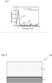
- FIG 3 shows the result of deep level transient spectroscopy (DLTS) analysis of the semiconductor device 1 according to Figure 1 .
- the curve with reference sign A shows a DLTS spectrum of untreated n-type 4H-SiC epitaxial layer 2 as-grown after step S1.
- the curve shows with reference sign B shows the DLTS spectrum of the epitaxial layer 2 after implantation of carbon ions in step S2 and annealing in step S3.
- the untreated semiconductor device 1 comprises a relatively high concentration of carbon vacancy.
- it comprises a concentration of Z 1/2 defects in the order of 10 12 /cm 3 .
- the defect level Z 1/2 is very close to the conduction band edge E C and would therefore negatively affect the performance of a finished semiconductor device 1.
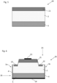
- processing steps for manufacturing a PIN diode 20 are shown with respect to Figures 4 to 6 .
- a first processing step shown in Figure 4 an n-type 4H-SiC epitaxial layer 2 is grown on a substrate 5. As described above, the epitaxial layer 2 will have a relatively high concentration of carbon vacancies V C .
- the epitaxial layer 2 is implanted with aluminum ions to form a highly doped p-type anode area 21. This is followed by a high temperature annealing step (not shown).
- Figure 6 shows the final p+-i-n structure of the PIN diode 20, further comprising implanted field relaxation layers 22 formed by conventional ion implantation.
- a metal anode electrode 23 and a metal cathode electrode 24 are formed on a top and bottom surface of the anode area 21 and the substrate 5, respectively.
- the anode electrode 23 and the cathode electrode 24 may be formed by electron-beam deposition. Forming of the field relaxation layers 22, the anode electrode 23 and the cathode electrode 24 may result in the generation of further carbon vacancies V C in the epitaxial layer 2 acting as an intrinsic drift layer of the PIN diode 20.
- two implantation areas 4 are formed on the sidewalls 3a of the PIN diode 20 (also shown in Figure 6 ). Implantation of Carbon or other ions in the implantation areas 4 and optional subsequent annealing of the epitaxial layer 2 will result in a reduced carbon vacancy V C concentration in the epitaxial layer 2 acting as a drift layer. This is indicated in Figure 6 by the lighter shading of the epitaxial layer 2.
- the side implantation and subsequent annealing will also generate ON1 and ON2 levels.
- the presence of ON1 and ON2 levels in the epitaxial layer 2 does not influence the performance of the PIN diode 20.
- forming of the field relaxation areas 22 is performed by frontside processing of the epitaxial layer 2 on a wafer or other substrate 5.
- formation of the electrodes 23 and 24 is implemented by conventional metallization procedures from the front and back surfaces of the semiconductor device 1.
- semiconductor devices 1 typically a relatively large number of semiconductor devices 1, such as PIN diodes 20 are formed together on a common wafer or other substrate 5.
- an area of the wafer or other substrate 5 corresponding to the PIN diode 20 may be separated from similar semiconductor circuit components grown on the same wafer or other substrate 5 by dicing. Thereby, individual semiconductor chips are formed, which may then be installed with the [0001] crystallographic axis pointing sideways into an ion implantation system to implant carbon ions through the sidewalls 3a of the individual semiconductor chips.
- a modified target holder carrying one or more semiconductor chips may be employed.
- a first implantation direction 25 for implanting ions into the field relaxation area 22 of the epitaxial layer 2 is orthogonal to a second implantation direction 26 for implanting ions into the implantation area 4.
- the implantation area 4 extends over the entire side surface of the semiconductor material, comprising the substrate 5 and the epitaxial layer 2.
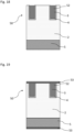
- FIGs 7 to 10 show processing steps for manufacturing a bipolar junction transistor (BJT) 30, exemplarily an NPN transistor, according to an embodiment of the present disclosure.
- BJT bipolar junction transistor
- an n-type collector 31 made from a semiconductor material comprising carbon, such as 4H-SiC or 6H-SiC, is provided.
- a p-type base 32 is epitaxially grown on the n-type collector 31 ( Figure 8 ).
- an n-type emitter layer 33 is epitaxially grown on the p-type base 32 ( Figure 9 ).
- gate electrodes as shown in Figure 10 .
- highly doped p-type layers 34 are formed in the p-type base 34.
- a gate electrode 35 is formed on a top surface of the highly doped p-type layer 34
- an emitter electrode 36 is formed on a top surface of the n-type emitter 33
- a collector electrode 36 is formed on a bottom surface of the n-type collector 31.
- the semiconductor material of both the n-type collector 31 as well as the n-type emitter 33 will comprise an increased concentration of carbon vacancies V C present in the respective epitaxial layers 2 as-grown and/or further processed during a processing of the BJT 30.
- implantation areas 4 are formed on sidewalls 3a of the BJT 30 as described above. The presence of the implantation areas 4 will result in the formation of carbon interstitials C I and thus a reduction of the carbon vacancy V C .
- a PNP BJT may be formed using the disclosed side implantation method, comprising a n-type base with a reduced carbon vacancy V C after annealing with respect to the epitaxial layer later forming the base as-grown.
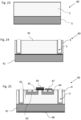
- FIGS 11 and 12 show two stages of manufacturing an insulated-gate bipolar transistor (IGBT) 40. Initially, an n-type base 42 made from 4H-SiC or 6H-SiC is epitaxially grown on a p-type collector 41, as shown in Figure 11 .
- IGBT insulated-gate bipolar transistor
- n-type base 42 As shown in Figure 12 , within the n-type base 42, two p-type base wells 43 are formed by ion implantation through a top surface of the n-type base 42. Therein, a total of four n-type areas 44 are formed by either plasma immersion ion implantation (PIII) or conventional ion implantation.
- PIII plasma immersion ion implantation
- an oxide layer 45 serving as electrical insulator, is formed in the central area of the n-type base 42 between right (inner) n-type area 44 of the left p-type base well 43 and the left (inner) n-type area 44 of the right p-type base well 43.
- an insulated gate electrode 46 is formed on top of the oxide layer 45.
- one or more emitter electrodes 47 are formed on top surface of the n-type areas 44.
- a collector electrode 47 is formed on the back surface of the p-type collector 41.
- the electrodes 46, 47 and 48 may be formed by e-beam deposition.
- a buffer layer can be present at the interface between the n-type base 42 and the p-type collector 41.
- the n-type base layer 42 will have a high carbon vacancy V C concentration after forming the IGBT 40.
- implantation areas 4 are formed on sidewalls 3a of the IGBT 40 before annealing the n-type base 42. As described above, this will remove carbon vacancy V C from the base 42 and result in the generation of ON1 and ON2 in the n-type layers 42 and 44. However, the generated ON1 and ON2 are not harmful for the manufactured semiconductor device, e.g. the IGBT 40.
- the process has been described for an IGBT 40 comprising an n-type base layer 42, the same applies for an IGBT fabricated starting from an n-type collector layer and having a p-type base layer.
- the implantation area 4 is placed outside an electrically active area of the respective semiconductor device 1.
- the finished semiconductor device 1 may comprise a high concentration of the implanted species, such as carbon, in the implantation area 4.
- the implanted species such as carbon
- a remaining implantation defect area of the implantation area 4 will still contain amorphous silicon indicative of the previous side implantation step.
- no long oxidation time and no long HF etching time are required.
- carbon vacancy V C can be reduced in epitaxial layers 2 of any thickness.
- the process is especially suited for very thick drift layers of more than 50um thickness.
- the method can be applied to both unipolar and bipolar devices. Some processing steps, such as annealing, can be carried out at lower temperatures compared to prior art methods.
- an implantation through a sidewall of the epitaxial layer 2 can also be achieved using one or more trenches formed in an epitaxial layer 2 as described in further detail below. This may also be used in semiconductor devices, in which trenches are formed throughout a normal manufacturing process anyhow.
- FIG. 13 schematically shows a cross-sectional view of a semiconductor device 1 according to an embodiment of the disclosure.
- the semiconductor device 1 comprises an epitaxial layer 2 of a reduced concentration of carbon vacancy Vc.
- the semiconductor device 1 comprises, besides the epitaxial layer 2, a trench 3 extending in the epitaxial layer 2.
- the trench 3 comprises an implantation layer 4 in form of an implanted carbon layer, which is provided on the trench sidewalls 3a and a trench bottom 3b.
- carbon (C) one of boron (B), aluminum (Al), germanium (Ge), nitrogen (N), phosphorus (P), arsenic (As), oxygen (O), sulfur (S), hydrogen (H), argon (Ar) or silicon (Si) may be implanted.
- the implantation may be performed by plasma immersion ion implantation (PIII).
- PIII can also be performed on the top surface of the epitaxial layer 2, e.g. the main or front surface of the epitaxial layer 2, at which the trench 3 opens.
- PIII can also be performed parallel to the [0001] crystallographic axis (not shown in Figure 13 ). If PIII is applied at the front surface of the epitaxial layer 2, the formed PIII sublayer needs to be removed later by dry etching. However, as detailed below, this is not necessary for surfaces within the trench 3.
- the epitaxial layer 2 comprises an epitaxial sublayer 2a of a reduced concentration of carbon vacancy Vc. As shown, the epitaxial sublayer 2a of the reduced concentration of carbon vacancy Vc extends perpendicular to a [0001] crystallographic axis and parallel to this axis, and a thickness of the epitaxial sublayer 2a of the reduced carbon vacancy at least corresponds to a depth D T of the trench 3.
- the epitaxial layer 2 based on Silicon Carbon (SiC) comprises an amount of electrically active levels, corresponding to the carbon vacancy (Vc) concentration, which cannot be neglected.
- Vc carbon vacancy
- carbon vacancies V C can be removed in an area of the epitaxial layer 2 below the implantation surface, for example a sublayer of 100 ⁇ m thickness along the [0001] crystallographic axis.
- a suitable species such as B, Al, C, Si, Ge, N, P, As, O, S, F, H or Ar
- annealing the implantation area at 1600°C carbon vacancies V C can be removed in an area of the epitaxial layer 2 below the implantation surface, for example a sublayer of 100 ⁇ m thickness along the [0001] crystallographic axis.
- carbon vacancies V C can be removed over a much larger distance. For example, a horizontal diffusion length of several millimeters can be achieved.
- the PIII implanted species are confined in a relatively small space, for example a sublayer having a thickness of less than 50 nm. This causes stress that releases C I .
- the epitaxial layer 2 comprises the trench 3 with the implantation layer 4.
- the carbon layer 4 for example, has a thickness of less than 50 nm.
- the PIII carbon in the trench sidewalls 3a and trench bottom 3b provides carbon interstitials C I , which are defects, and which can migrate perpendicular to the [0001] crystallographic axis and recombine with the electrically active defects providing the carbon vacancy Vc as detailed above.
- filled circles in the epitaxial layer 2 are shown to illustrate the carbon interstitials C I .
- the trench 3 extends parallel to or along the [0001] crystallographic axis of the epitaxial layer 2.
- the trench 3 may also extend at an angle ⁇ relative to the [0001] crystallographic axis.
- L is a length of the PIII carbon layer 4 from a trench inlet to a trench ending.
- L corresponds to the trench depth D T .
- D is a distance, which is measured parallel to the [0001] crystallographic axis, from a beginning of the implantation layer 4 to an ending of the implantation layer 4 in the trench 3.
- D corresponds to the trench depth D T .
- ⁇ is an angle between L and D. In the exemplary embodiment of Figure 13 , ⁇ is zero.
- FIG 14 schematically shows a deep level transient spectroscopy (DLTS) spectrum of an epitaxial layer 2 being treated by a method according to an embodiment.
- the epitaxial layer 2 is made of 4H-SiC.
- the DLTS spectrum is shown for the epitaxial layer 2 with and without Carbon diffusion perpendicular to the [0001] crystallographic axis.
- the curve indicated by the reference sign A represents the DLTS spectrum in untreated material, that means the level Z 1/2 is in a range of 10 12 1/cm 3 .
- the curve indicated by the reference sign B represents the DLTS spectrum after implantation. It can be seen that no level Z 1/2 defects can be detected.
- the concentration of the level Z 1/2 that means the negative charge state of the electrically active defects providing the carbon vacancy V C , is below a detection limit.
- a manufacturing method according to an embodiment will be explained based on the flow diagram of Figure 26 and specific embodiments as shown in Figures 15 to 19 .
- the manufacturing method is suitable for providing a semiconductor device 1 with an epitaxial layer 2 with a reduced concentration of electrically active carbon levels in the epitaxial layer 2.
- the semiconductor device 1 produced according to the steps shown in Figures 3 to 7 is a Junction Barrier Schottky (JBS) diode 50.
- JBS Junction Barrier Schottky
- the method comprises providing an epitaxial layer 2 on a substrate 5 (see Figure 26 and Figure 15 ).
- the embodiment of Figure 15 shows an n-type 4H-SiC epitaxial layer 2 with a doping concentration in a range from 10 14 1/cm 3 to 10 16 1/cm 3 being grown on a 4H-SiC substrate with a doping concentration of 10 18 1/cm 3 .
- the epitaxial layer thickness and doping are selected according to a voltage class of the semiconductor device 1.
- the method comprises providing a photoresist layer 51 on the epitaxial layer 2 (see Figure 26 and Figure 16 ) and exposing the photoresist layer 51 with electromagnetic radiation using a mask (not depicted).
- the photoresist layer 51 being deposited on the epitaxial layer surface is patterned by photolithography according to the desired shape/dimensions of the trenches 3 which are provided in a subsequent step.
- the method comprises providing two trenches 3 in the epitaxial layer 2 (see Figure 26 and Figure 16 ).
- the epitaxial layer 2 is etched by reactive ion etching (RIE) in order to form the trenches 3.
- RIE reactive ion etching
- the trenches 2 can have any cross section, such as square, round, rectangular, or polygonal. If D T is the depth of the trench 3 and 1 the width of the cross section, deep trenches 3 (D T >>1) can also be formed.
- the method comprises implanting carbon or another suitable species in each of the trenches 3 (see Figure 26 and Figure 17 ).
- the trench sidewalls 3a and the trench bottom 3b of the trenches 3 are implanted with Carbon by plasma immersion ion implantation (PIII) to obtain the maximum doping concentration but not exceeding a solubility limit.
- the method comprises filling the trenches 3 with p-type polysilicon 52 (see Figure 26 and Figure 18 ).
- the step of filling the trenches 3 with p-type polysilicon 52 may be, alternatively, carried out after removing the photoresist layer 51 (see description in the context of step S16 below). As detailed later, filling the trenches 3 may assist in forming contacts, and generally will improve the mechanical stability of the finished semiconductor device 1.
- the method comprises carrying out an annealing process such that carbon ion diffusion from the at least one trench 3 perpendicular and/or parallel to a crystallographic [0001] axis of the at least one epitaxial layer 2 is induced (see Figure 26 ; the diffusion process is not illustrated in Figure 18 ; Figure 13 illustrates the diffusion process of the carbon interstitials C I ).
- Carbon is diffused by annealing at a temperature of less than 1600 °C for a time in the range from 5 minutes to 600 minutes.
- oxygen plasma ashing is, for example, employed to remove the photoresist layer 51.
- the photoresist layer 51 can be removed after PIII in steps S14, and a graphitic cap is then formed on the epitaxial layer surface so to ensure low surface roughness on the trench walls 3a during activation. After annealing, a graphitic cap can be removed by oxygen plasma ashing.
- the epitaxial layer 2 has a V C concentration below the detection limit.
- the method comprises providing contact layers 53 according to a functioning of the semiconductor device 1.
- metal is deposited on an epitaxial layer surface and on a backside for Schottky/ohmic contact formation.
- the manufacturing method according to the embodiment of Figure 26 will also be described based on the Figures 20 to 22 .
- the semiconductor device 1 produced according to the steps shown in Figures 20 to 22 is a Bipolar Junction Transistor (BJT) 30.
- the BJT 30 is an NPN transistor.
- Figure 20 schematically shows a first step of the method for producing the BJT 30.
- Two epitaxial layers 2 are provided, which are grown on a substrate 5.
- the Figure 20 shows an upper n-type 4H-SiC epitaxial layer 2 with a doping concentration in a range from 10 14 1/cm 3 to 10 16 1/cm 3 . It is grown on a middle epitaxial p-type epitaxial layer 2 with a doping concentration in a range from 10 14 1/cm 3 to 10 16 1/cm 3 on top of a 4H-SiC substrate 5 with a doping concentration of 10 18 1/cm 3 .
- the layer thicknesses and doping concentrations are selected according to the voltage class of the BJT 30.
- FIG 21 schematically shows a second step of the method for producing the BJT 30.
- the epitaxial layers 2 are etched by reactive ion etching (RIE) in order to form two trenches 3.
- the trenches 3 can have any cross section, such as square, round, rectangular, or polygonal.
- Carbon is implanted in the trenches 3 by PIII and later diffused by annealing. After Carbon diffusion the upper epitaxial layer 2 corresponding to the n-type emitter 33 as well as the substrate 5 corresponding to the n-type collector 31 have a low carbon vacancy concentration.
- Trench sidewalls 3a and an epitaxial layer top can be protected by a graphitic cap.
- Figure 22 schematically shows a third step of a method for producing the BJT 30.
- oxygen plasma ashing is employed to remove the graphitic cap.
- high-doped p-type layers 34 are formed and metal is deposited for providing gate electrodes 35, emitter electrodes 36, and collector electrodes 37.
- the manufacturing method according to the embodiment of Figure 26 will also be described based on the Figures 11 to 13 .
- the semiconductor device 1 produced according to the steps shown in Figures 23 to 25 is an insulated-gate bipolar transistor (IGBT) 40.
- IGBT insulated-gate bipolar transistor
- Figure 23 schematically shows a first step of the method for producing the IGBT 40.
- the Figure 23 shows an n-type 4H-SiC epitaxial layer 2 with a doping concentration in a range from 10 14 1/cm 3 to 10 16 1/cm 3 on top of a 4H-SiC substrate 5 with a doping concentration of 10 18 1/cm 3 .
- the epitaxial layer and substrate thicknesses and doping concentrations are selected according to the voltage class of the IGBT 40.
- Figure 24 schematically shows a second step of the method for producing the IGBT 40.
- the epitaxial layer 2 is etched by reactive ion etching (RIE) in order to form two trenches 3.
- a depth D T of the trenches 3 corresponds to a thickness of the epitaxial layer 2.
- a relatively deep trench 3 as shown in Figure 24 assists in removing carbon vacancies throughout a relatively thick epitaxial layer 2.
- the trenches 3 can have any cross section, such as square, round, rectangular, or polygonal.
- Carbon is implanted in the trenches 3 by PIII and later diffused by annealing. After Carbon diffusion the epitaxial layer 2 comprising an n-type base 42 has a low carbon vacancy concentration.
- the trench sidewalls 3a and an epitaxial layer top can be protected by a graphitic cap.
- FIG 25 schematically shows a third step of the method for producing the IGBT 40.
- oxygen plasma ashing is employed to remove the graphitic cap.
- Two p-type base well 43 are formed by ion implantation and a total of four n-type areas 44 are formed inside them by either PIII or by ion implantation. Ion implantation would be carried out in a state, in which the device manufacturing is in the state shown in Figure 24 .
- a gate electrode 46, an emitter electrode 47, and a collector electrode 48 are formed by e-beam deposition.
- the gate electrode 48 is provided with an oxide layer 45, which insulated the gate from the epitaxial layer 2 with the active electrical areas formed therein.
- a buffer layer can also be provided at the base/collector interface (not shown in Figure 25 ).
Landscapes
- Recrystallisation Techniques (AREA)
- Chemical & Material Sciences (AREA)
- Crystallography & Structural Chemistry (AREA)
Description
- The present disclosure relates to semiconductor devices comprising at least one epitaxial layer made from a first semiconductor material comprising carbon, wherein at least one part of the epitaxial layer has a reduced concentration of carbon vacancies with respect to the first semiconductor material of the at least one epitaxial layer as-grown. The present disclosure further relates to methods for manufacturing such semiconductor devices.
-
US 7 754 589 B2 relates to a method for improving the quality of a SiC layer by effectively reducing or eliminating the carrier trapping centers in the as-grown SiC crystal. - The process described in the following with reference to
fig. 27 , which is based on the implantation of C atoms into the top surface of a SiC epitaxial layer, is similar to one of the alternative processes disclosed in this document. -
US2013/183820 A1 discloses a further method to reduce the carbon vacancy concentration in a SiC semiconductor body. That method comprises forming trenches in a SiC body by means of RIE followed by thermal etching, forming a C-rich layer on the sidewalls of said trenches and diffusing them into the semiconductor body by heat treatment. -
US 2014/361312 A1 relates to a SiC reverse blocking MOSFET that includes an active region including a MOS gate structure and a breakdown voltage structure portion surrounding the outer circumference of the active region, which are provided on the surface side of a SiC-n- drift layer that is grown on one main surface of a p+ SiC substrate. -
US 2015/333190 A1 relates to a semiconductor device that includes a semiconductor layer made of a wide bandgap semiconductor, a trench that is selectively formed on a surface portion of the semiconductor layer and that defines a unit cell having a predetermined shape on the surface portion, and a surface electrode that is embedded in the trench so as to cover an upper surface of the unit cell and that forms a Schottky junction between the unit cell and the surface electrode, and side surfaces of the trench are formed of only a plurality of planes that have plane orientations crystallographically equivalent to each other. -
US 2015/108500 A1 discloses a semiconductor device comprising a semiconductor body of a first semiconductor material, wherein at least a part of the semiconductor body constitutes a drift zone of a first conductivity type. The semiconductor device further comprises a channel layer structure comprising a semiconductor heterojunction between first and second semiconductor layers electrically coupled to the drift zone. The first and second semiconductor layers include semiconductor materials that are different to the first semiconductor material. -
US 9 093 568 B1 - Embodiments of the disclosure relate to improved semiconductor devices and methods for their manufacturing. Exemplarily, there is a need for semiconductor devices that have an improved lifetime, low defect density and/or can be manufactured in a flexible way using conventional semiconductor processing steps.
- The invention is defined by the attached set of claims. Further details of the disclosed devices and methods are provided in the following, which are helpful for understanding the claimed invention.
- According to a first aspect, a semiconductor device comprising at least one epitaxial layer made from a first semiconductor material comprising carbon and having a [0001] crystallographic axis is provided. At least one implantation area is formed at a sidewall of the epitaxial layer, a normal direction of the sidewall being perpendicular to the [0001] crystallographic axis. At least one part of the epitaxial layer has a reduced concentration of carbon vacancies with respect to the first semiconductor material of the at least one epitaxial layer as-grown.
- The at least one at least one epitaxial layer made from a first semiconductor material comprises at least one of n-type 4H-SiC or n-type 6H-SiC semiconductor material. The at least one implantation area comprises an implanted species, comprising at least one of carbon ions or silicon ions. The at least one part of the epitaxial layer is adjacent to the sidewall and has a concentration of carbon vacancy Z1/2 of below 1010/cm3.
- By providing an implantation area at a sidewall of an epitaxial layer, implantation can be performed independent of other processing steps, which are typically performed in parallel to the [0001] crystallographic axis, e.g. on or through the front face of the epitaxial layer. At the same time, motility of an implanted species is improved, which simplifies a later annealing of the at least one epitaxial layer and results in a reduced concentration of carbon vacancies therein.
- According to at least one embodiment, the at least one implantation area is formed on one of a plurality of sidewalls of at least one semiconductor chip comprising the at least one epitaxial layer. Implanting a species through a sidewall of a semiconductor chip allows the reduction of carbon vacancies on already separated, almost finished semiconductor circuit component.
- According to at least one embodiment, the semiconductor device comprises at least one trench having two sidewalls formed in the at least one epitaxial layer. The at least one implantation area is formed on at least one of the two sidewalls of the at least one trench. The at least one part of the epitaxial layer corresponds to a sublayer extending in a plane perpendicular to the [0001] crystallographic axis, wherein a thickness of the sublayer corresponds to or exceeds a depth of the at least one trench. Use of trenches allows the implantation of a species on a vertical side-wall of an epitaxial layers having a relatively large spatial extent.
- In at least one embodiment, the semiconductor device further comprises at least one electrode formed on a top or bottom surface of the at least one epitaxial layer, thereby forming an electrically active area, wherein the at least one implantation area is formed outside of an electrically active area. For example, the at least one implantation area may be formed in spatial proximity to the electrically active area of the semiconductor device. Such a spatial arrangement allows the reduction of carbon vacancies in the electrically active area without disturbing any elements within the electrically active area implementing a function of the semiconductor device.
- For example, the at least one implantation area may comprises an implantation defect area, comprising amorphous silicon.
- According to different embodiments, the semiconductor device may comprise different power electronic components, such as a PIN diode, a BJT, an IGBT, or a JBS diode.
- According to a second aspect of the disclosure, a method for manufacturing a semiconductor device is provided. The method comprises growing at least one epitaxial layer made from a first semiconductor material comprising carbon and having a [0001] crystallographic axis, and implanting ions through at least one sidewall of the at least one epitaxial layer in a direction perpendicular to the [0001] crystallographic axis to form at least one implantation area, thereby reducing a concentration of carbon vacancies in the first semiconductor material with respect to the at least one epitaxial layer as-grown.
- The at least one at least one epitaxial layer made from a first semiconductor material comprises at least one of n-type 4H-SiC or n-type 6H-SiC semiconductor material. The implanted ions in particular comprise at least one of carbon ions and silicon ions. The first semiconductor material of the finished semiconductor device has a concentration of carbon vacancy Z1/2 of below 1010/cm3.
- The above steps enable the manufacturing of a semiconductor device according to first aspect. They enable an improved degree of flexibility during manufacturing. In particular, the step of implanting ions can be performed towards the end of the manufacturing process after other steps negatively affecting carbon vacancies of the at least one epitaxial layer have been completed.
- According to at least one embodiment, the method further comprises at least one of annealing or proton irradiating the at least one epitaxial layer to further reduce the concentration of carbon vacancies in the first semiconductor material with respect to the at least one epitaxial layer after implanting ions. Annealing or proton irradiation helps to diffuse generated carbon interstitials.
- According to at least one embodiment, before implanting ions through at least one sidewall, the method further comprises: performing a plurality of processing steps to form at least one semiconductor circuit component comprising at least parts of the at least one epitaxial layer; and separating the at least one semiconductor circuit component to obtain a semiconductor chip having a top surface perpendicular to the [0001] crystallographic axis and a plurality of sidewalls perpendicular to the top surface. Implanting ions through sidewalls of semiconductor chips enables the reduction of carbon vacancies in a separated, essentially finished semiconductor component.
- According to another embodiment, the method further comprises forming at least one trench having two sidewalls within the at least one epitaxial layer, wherein implanting ions through at least one sidewall comprises plasma immersion ion implanting (PIII) of at least one of carbon (C) ions or silicon (Si) ions through the two sidewalls of the at least one trench.
- Further aspects, embodiments and advantages of the present invention are disclosed in the following detailed description of embodiments as well as the attached set of claims.
- The method for manufacturing a semiconductor device according to the second aspect described above is particularly suitable for manufacturing the semiconductor device according to the first aspect. Features and advantages described in connection with the semiconductor device can therefore be used in the manufacturing method and vice versa.
- Thus, every feature described with respect to one of the aspects is also disclosed herein with respect to the other aspect, even if the respective feature is not explicitly mentioned in the context of the specific aspect.
- The accompanying figures are included to provide a further understanding. In the figures, elements of the same structure and/or functionality may be referenced by the same reference signs. It is to be understood that the embodiments shown in the figures are illustrative representations and are not necessarily drawn to scale.
-
Figure 1 shows, in a schematic manner, a semiconductor device according to an embodiment of the disclosure. -
Figure 2 shows, in a schematic manner, a method for manufacturing a semiconductor device according to an embodiment of the disclosure. -
Figure 3 shows DLTS spectra of an epitaxial layer according toFigure 1 before and after implanting and annealing. -
Figures 4 to 6 show steps for manufacturing a PIN diode according to an embodiment of the disclosure. -
Figures 7 to 10 show steps for manufacturing a BJT according to an embodiment of the disclosure. -
Figures 11 and 12 show steps for manufacturing an IGBT according to an embodiment of the disclosure. -
Figure 13 shows, in a schematic manner, a semiconductor device comprising a trench according to an embodiment of the disclosure. -
Figure 14 shows DLTS spectra of an epitaxial layer according toFigure 13 before and after implantation and annealing. -
Figures 15 to 19 show steps for manufacturing a JBS diode according to another embodiment of the disclosure. -
Figures 20 to 22 show steps for manufacturing a BJT according to another embodiment of the disclosure. -
Figures 23 to 25 show steps for manufacturing an IGBT according to another embodiment of the disclosure. -
Figure 26 shows, in a schematic manner, a method for producing a semiconductor device according to an embodiment of the disclosure. -
Figure 27 shows, in a schematic manner, the removal of carbon vacancies through a top surface of a semiconductor device, which is part of the technological background of the present invention. - While the disclosure is amenable to various modifications and alternative forms, specifics thereof have been shown by way of example in the figures and will be described in detail. It should be understood, however, that the intention is not to limit the disclosure to the particular embodiments described. On the contrary, the intention is to cover all modifications, equivalents, and alternatives falling within the scope of the disclosure defined by the appended claims.
- Before various embodiments of the present disclosure are described in more detail, at first some challenges encountered in conventional silicon carbide semiconductor materials and their processing are discussed.
- The so-called carbon vacancy (VC) is a technologically relevant, electrically active point defect in n-type 4H silicon carbide (4H-SiC). The presence of carbon vacancy gives rise to two levels in the bandgap of the semiconductor material, referred to as Z1/2 and EH6/7, located at 0.65 eV and 1.6 eV below the conduction band edge (EC), respectively. As the level of Z1/2 defects is particularly close to the conduction band edge, it acts as a recombination center, affecting the lifetime, forward voltage drop of bipolar devices and leakage current in unipolar devices formed from such semiconductor materials.
- In principle, it is possible to remove a carbon vacancy from an epitaxial layer as-grown as shown in
Figure 27 . - A
semiconductor device 1 comprises a 4H-SiC epitaxial layer 2 grown on a surface of asubstrate 5 in a [0001] crystallographic axis direction X, as defined by Miller-Bravais indices. The [0001] crystallographic axis typically corresponds to the normal direction of the surface of thesubstrate 5. As-grown, theepitaxial layer 2 will comprise a number of carbon vacancies VC throughout the 4H-SiC epitaxial layer 2. To reduce the concentration of carbon vacancy VC, atop surface area 4a is either oxidized at a temperature of 1050 to 1400°C. Alternatively, a shallow carbon ions may be implanted into thetop surface area 4a ofSiC epitaxial layer 2. Either approach will in the introduction of carbon interstitials CI into the 4H-SiC epitaxial layer 2. Then, theepitaxial layer 2 is annealed at a temperature in excess of 1500°C, resulting in a diffusion of the carbon interstitials CI throughout theepitaxial layer 2. The carbon interstitials CI can then recombine with the carbon vacancies VC. Consequently, theepitaxial layer 2 will have a reduced carbon vacancy concentration. - As shown in
Figure 27 , Carbon implantation is performed parallel to the [0001] crystallographic axis. After diffusion of carbon interstitials CI, reactive ion etching (RIE) or chemical mechanical polishing (CMP) is used in order to remove the C-implanted layer formed in thetop surface area 4a. A similar situation would occur if oxidation is employed for carbon vacancy VC reduction, where the oxide layer needs to be removed using hydrofluoric acid (HF). - Thus, the method for reducing carbon vacancy described above can only be carried out relatively early in a manufacturing processes, e.g. on the
epitaxial layer 2 as-received. While this results in a 4H-SiC epitaxial layer 2 having a reduced concentration of carbon vacancies VC towards the start of the manufacturing of asemiconductor device 1, subsequent processing steps such as activation of a highly doped p+ area or annealing of electrodes of an semiconductor circuit component, result in a regeneration of carbon vacancies VC in theepitaxial layer 2. Once the carbon vacancies VC have been re-generated, a second Carbon ion implantation cannot be performed, as this would require implanting Carbon into electrically active areas of the semiconductor device, such as an anode area or electrode. Moreover, oxidation cannot be performed, as this would consume parts of the active circuit structures in case of relatively thickepitaxial layers 2, e.g.epitaxial layers 2 having a thickness of 100 µm or more. - The present disclosure aims to describe alternative methods and devices having a reduced carbon vacancy concentration as compared to an epitaxial layer as-grown.
-
Figure 1 shows asemiconductor device 1 according to an embodiment of the present disclosure. Steps S1 to S3 of a method for reducing carbon vacancy VC of anepitaxial layer 2 of thesemiconductor device 1 are shown inFigure 2 . - In a step S1, the
epitaxial layer 2 is grown on asubstrate 5 or other epitaxial layer (not shown). Initially, theepitaxial layer 2 will comprise a relatively high concentration of carbon vacancy VC. For example, untreated n-type 4H-SiC semiconductor material of theepitaxial layer 2 may have comprise 1012 Z1/2 defects per cm3. - Thus, in step S2, ions, for example carbon (C) ions, aluminum (Al) ions or silicon (Si) ions, are implanted through a
sidewall 3a to form animplantation area 4 in the semiconductor material. Contrary to the situation shown inFigure 27 , in the embodiment shown inFigure 1 , ions are implanted throughsidewalls 3a to formimplantation areas 4 in a plane perpendicular to a top surface of the semiconductor device. That is to say, the implantation direction is perpendicular to the [0001] crystallographic axis direction X of theepitaxial layer 2. The side implantation may be performed at room temperature. - In the embodiment shown in
Figure 1 , carbon ions are implanted through twoopposite sidewalls 3a to form carbon interstitial CI in twoimplantation areas 4. It is also possible to implant ions through asingle sidewall 3a to form asingle implantation area 4, or to implant ions through three or foursidewalls 31, for example all sidewalls of a rectangular semiconductor chip. In the described embodiment, side implantation of Carbon on a 3-5 x 1016 cm-3 N-dopedepitaxial layer 2 was carried out. One or more side implantation energies can be chosen so that the implantation profile will be outside the active electric area of thesemiconductor device 1. For example, three different implantation stages with energies in the range of 10 to 200 keV may be used. Side implantation doses can range from 1010 to 1016 cm-2. - As shown in
Figure 1 , step S2 may be carried out immediately after growing the epitaxial layer S1. However, it is also possible to form theimplantation areas 4 towards the end of manufacturing thesemiconductor device 1 as later described with regard to various specific semiconductor devices. - Side implantation can be followed by an optional, separate diffusion step S3. For example, the
epitaxial layer 2 may be annealed at temperatures in excess of 1000°C for periods between 1 minute and 10 hours depending on the thickness of theepitaxial layer 2. The thickness of theepitaxial layer 2 may lie in a range of 5 to 150 µm for example. In the described embodiment, theepitaxial layer 2 a relatively short annealing step is carried out at a temperature of 1500°C for a period of 5 minutes. During this period, the generated carbon interstitials CI further diffuse throughout theepitaxial layer 2. Alternatively or in addition, proton irradiation may be used to further diffuse the generated carbon interstitials CI. For example, proton irradiation at or below 10 keV may be used. - Alternatively, side implantation with no subsequent diffusion step can be carried out on a finished semiconductor component. For example, after implantation of carbon with energies equal or higher than 300 keV, sufficient diffusion of carbon interstitials CI takes place without an additional diffusion step.
- It has been found that point defects in crystal structure of the
epitaxial layer 2 can migrate quickly and thus a relatively long distances perpendicular to the [0001] crystallographic axis direction X. For example, carbon interstitials can diffuse long distances perpendicular to [0001] direction after 10 keV proton irradiation even at room temperature. This in turn significantly reduces carbon vacancy VC throughout theepitaxial layer 2. For example, using the parameters described above, a horizontal diffusion length of several millimeters can be achieved, resulting in a significant reduction of carbon vacancy VC throughout the entire width of theepitaxial layer 2 of a semiconductor chip having an edge length of 5 mm, for example. For example, a concentration of carbon vacancies VC may be reduced by two or more orders of magnitude as compared with theepitaxial layer 2 as-grown. -
Figure 3 shows the result of deep level transient spectroscopy (DLTS) analysis of thesemiconductor device 1 according toFigure 1 . Therein, the curve with reference sign A shows a DLTS spectrum of untreated n-type 4H-SiC epitaxial layer 2 as-grown after step S1. The curve shows with reference sign B shows the DLTS spectrum of theepitaxial layer 2 after implantation of carbon ions in step S2 and annealing in step S3. As can be seen, after step S1, theuntreated semiconductor device 1 comprises a relatively high concentration of carbon vacancy. Exemplarily, it comprises a concentration of Z1/2 defects in the order of 1012/cm3. As detailed above, the defect level Z1/2 is very close to the conduction band edge EC and would therefore negatively affect the performance of afinished semiconductor device 1. - After implantation of carbon ions in step S2 and annealing of the epitaxial layer in step S3, no detectable amount of Z1/2 defects are present in the
semiconductor device 1. In addition, as can be seen inFigure 3 , the presence of so-called deep level ON1 and ON2 peaks that lie 0.84 eV and 1.1 eV below the conduction band edge EC, respectively, can be detected. ON1 and ON2 levels are associated with carbon diffusion and typically detected after the implantation of carbon ions as described above with regard toFigure 27 . Accordingly, side implantation of carbon ions throughsidewalls 3a of a semiconductor device greatly reduce the concentration of carbon vacancy VC of anepitaxial layer 2 with respect to the concentration of carbon vacancies VC in thesame epitaxial layer 2 as-grown. - In the following, manufacturing processes for
various semiconductor devices 1 are described in more detail. The described processing steps will make apparent that a side implementation as described above with regard toFigures 1 and 2 provides an enhanced degree of flexibility in the manufacturing ofsemiconductor devices 1. - At first, processing steps for manufacturing a
PIN diode 20 are shown with respect toFigures 4 to 6 . In a first processing step shown inFigure 4 , an n-type 4H-SiC epitaxial layer 2 is grown on asubstrate 5. As described above, theepitaxial layer 2 will have a relatively high concentration of carbon vacancies VC. In a next processing step shown inFigure 5 , theepitaxial layer 2 is implanted with aluminum ions to form a highly doped p-type anode area 21. This is followed by a high temperature annealing step (not shown). - During the annealing, further carbon vacancies VC are generated, even in the case carbon vacancies VC had been previously removed.
-
Figure 6 shows the final p+-i-n structure of thePIN diode 20, further comprising implanted field relaxation layers 22 formed by conventional ion implantation. In addition, ametal anode electrode 23 and ametal cathode electrode 24 are formed on a top and bottom surface of theanode area 21 and thesubstrate 5, respectively. Theanode electrode 23 and thecathode electrode 24 may be formed by electron-beam deposition. Forming of the field relaxation layers 22, theanode electrode 23 and thecathode electrode 24 may result in the generation of further carbon vacancies VC in theepitaxial layer 2 acting as an intrinsic drift layer of thePIN diode 20. - To improve the performance of the
PIN diode 20, and exemplarily of the n-type epitaxial layer 2, twoimplantation areas 4 are formed on thesidewalls 3a of the PIN diode 20 (also shown inFigure 6 ). Implantation of Carbon or other ions in theimplantation areas 4 and optional subsequent annealing of theepitaxial layer 2 will result in a reduced carbon vacancy VC concentration in theepitaxial layer 2 acting as a drift layer. This is indicated inFigure 6 by the lighter shading of theepitaxial layer 2. - As detailed above with
Figure 3 , the side implantation and subsequent annealing will also generate ON1 and ON2 levels. However, the presence of ON1 and ON2 levels in theepitaxial layer 2 does not influence the performance of thePIN diode 20. - In the described embodiment, forming of the
field relaxation areas 22 is performed by frontside processing of theepitaxial layer 2 on a wafer orother substrate 5. Similarly, formation of theelectrodes semiconductor device 1. For efficiency, typically a relatively large number ofsemiconductor devices 1, such asPIN diodes 20 are formed together on a common wafer orother substrate 5. - To implant ions in the
vertical implantation areas 4, an area of the wafer orother substrate 5 corresponding to thePIN diode 20 may be separated from similar semiconductor circuit components grown on the same wafer orother substrate 5 by dicing. Thereby, individual semiconductor chips are formed, which may then be installed with the [0001] crystallographic axis pointing sideways into an ion implantation system to implant carbon ions through thesidewalls 3a of the individual semiconductor chips. For this purpose, a modified target holder carrying one or more semiconductor chips may be employed. During implantation, afirst implantation direction 25 for implanting ions into thefield relaxation area 22 of theepitaxial layer 2 is orthogonal to asecond implantation direction 26 for implanting ions into theimplantation area 4. Moreover, due to the side implantation, theimplantation area 4 extends over the entire side surface of the semiconductor material, comprising thesubstrate 5 and theepitaxial layer 2. -
Figures 7 to 10 show processing steps for manufacturing a bipolar junction transistor (BJT) 30, exemplarily an NPN transistor, according to an embodiment of the present disclosure. In a first step shown inFigure 7 , an n-type collector 31 made from a semiconductor material comprising carbon, such as 4H-SiC or 6H-SiC, is provided. Subsequently, a p-type base 32 is epitaxially grown on the n-type collector 31 (Figure 8 ). Then, an n-type emitter layer 33 is epitaxially grown on the p-type base 32 (Figure 9 ). - Subsequently, selected areas of the
emitter 33 and corresponding top parts of the base 32 are etched to allow for the formation of gate electrodes as shown inFigure 10 . At the base of the etched trenches, highly doped p-type layers 34 are formed in the p-type base 34. Thereafter, agate electrode 35 is formed on a top surface of the highly doped p-type layer 34, anemitter electrode 36 is formed on a top surface of the n-type emitter 33, and acollector electrode 36 is formed on a bottom surface of the n-type collector 31. - The semiconductor material of both the n-
type collector 31 as well as the n-type emitter 33 will comprise an increased concentration of carbon vacancies VC present in therespective epitaxial layers 2 as-grown and/or further processed during a processing of theBJT 30. To reduce the carbon vacancy VC in thecollector 31 andemitter 33,implantation areas 4 are formed onsidewalls 3a of theBJT 30 as described above. The presence of theimplantation areas 4 will result in the formation of carbon interstitials CI and thus a reduction of the carbon vacancy VC. - While the manufacturing method shown in
Figures 7 to 10 has been described with respect to formation of an NPN BJT, similarly, a PNP BJT may be formed using the disclosed side implantation method, comprising a n-type base with a reduced carbon vacancy VC after annealing with respect to the epitaxial layer later forming the base as-grown. -
Figures 11 and 12 show two stages of manufacturing an insulated-gate bipolar transistor (IGBT) 40. Initially, an n-type base 42 made from 4H-SiC or 6H-SiC is epitaxially grown on a p-type collector 41, as shown inFigure 11 . - As shown in
Figure 12 , within the n-type base 42, two p-type base wells 43 are formed by ion implantation through a top surface of the n-type base 42. Therein, a total of four n-type areas 44 are formed by either plasma immersion ion implantation (PIII) or conventional ion implantation. - Thereafter, an
oxide layer 45, serving as electrical insulator, is formed in the central area of the n-type base 42 between right (inner) n-type area 44 of the left p-type base well 43 and the left (inner) n-type area 44 of the right p-type base well 43. On top of theoxide layer 45, aninsulated gate electrode 46 is formed. Moreover, one ormore emitter electrodes 47 are formed on top surface of the n-type areas 44. On the back surface of the p-type collector 41, acollector electrode 47 is formed. Theelectrodes - Although not shown in
Figure 12 , a buffer layer can be present at the interface between the n-type base 42 and the p-type collector 41. - As detailed above, the n-
type base layer 42 will have a high carbon vacancy VC concentration after forming theIGBT 40. To reduce the unwanted point defects,implantation areas 4 are formed onsidewalls 3a of theIGBT 40 before annealing the n-type base 42. As described above, this will remove carbon vacancy VC from thebase 42 and result in the generation of ON1 and ON2 in the n-type layers IGBT 40. Moreover, although the process has been described for anIGBT 40 comprising an n-type base layer 42, the same applies for an IGBT fabricated starting from an n-type collector layer and having a p-type base layer. - It is noted that in the examples described above with reference to
Figures 4 to 12 , it is not necessary to remove theimplantation areas 4 after device manufacturing. In each case, theimplantation area 4 is placed outside an electrically active area of therespective semiconductor device 1. Thus, no additional RIE or CMP step is required as part of the disclosed manufacturing method, and thefinished semiconductor device 1 may comprise a high concentration of the implanted species, such as carbon, in theimplantation area 4. Even in the case that an part of theimplantation area 4 comprising the implanted species is removed after annealing, for example by RIE or CMP of thesidewalls 3a of the finished semiconductor chip, a remaining implantation defect area of theimplantation area 4 will still contain amorphous silicon indicative of the previous side implantation step. Similarly, compared to the oxidation method detailed above with respect toFigure 27 , no long oxidation time and no long HF etching time are required. - The described methods and devices have further advantages. For example, carbon vacancy VC can be reduced in
epitaxial layers 2 of any thickness. The process is especially suited for very thick drift layers of more than 50um thickness. The method can be applied to both unipolar and bipolar devices. Some processing steps, such as annealing, can be carried out at lower temperatures compared to prior art methods. - The above steps for implanting ions through one or more sidewalls 3a of an
individual semiconductor device 1 are particularly useful if the electrically active area of the finished device does not exceed the diffusion length of the implanted species. This will be the case for many typical power components, such as thePIN diode 20, theBJT 30 and theIGBT 40 described above. However, in the case of relatively large electrically active areas or in the case that carbon vacancy VC removal is required before separation of individual semiconductor circuit component, an implantation through a sidewall of theepitaxial layer 2 can also be achieved using one or more trenches formed in anepitaxial layer 2 as described in further detail below. This may also be used in semiconductor devices, in which trenches are formed throughout a normal manufacturing process anyhow. -
Figure 13 schematically shows a cross-sectional view of asemiconductor device 1 according to an embodiment of the disclosure. Thesemiconductor device 1 comprises anepitaxial layer 2 of a reduced concentration of carbon vacancy Vc. Thesemiconductor device 1 comprises, besides theepitaxial layer 2, atrench 3 extending in theepitaxial layer 2. Thetrench 3 comprises animplantation layer 4 in form of an implanted carbon layer, which is provided on thetrench sidewalls 3a and atrench bottom 3b. Instead of carbon (C), one of boron (B), aluminum (Al), germanium (Ge), nitrogen (N), phosphorus (P), arsenic (As), oxygen (O), sulfur (S), hydrogen (H), argon (Ar) or silicon (Si) may be implanted. - For example, the implantation may be performed by plasma immersion ion implantation (PIII). PIII can also be performed on the top surface of the
epitaxial layer 2, e.g. the main or front surface of theepitaxial layer 2, at which thetrench 3 opens. Thus, PIII can also be performed parallel to the [0001] crystallographic axis (not shown inFigure 13 ). If PIII is applied at the front surface of theepitaxial layer 2, the formed PIII sublayer needs to be removed later by dry etching. However, as detailed below, this is not necessary for surfaces within thetrench 3. - The
epitaxial layer 2 comprises anepitaxial sublayer 2a of a reduced concentration of carbon vacancy Vc. As shown, theepitaxial sublayer 2a of the reduced concentration of carbon vacancy Vc extends perpendicular to a [0001] crystallographic axis and parallel to this axis, and a thickness of theepitaxial sublayer 2a of the reduced carbon vacancy at least corresponds to a depth DT of thetrench 3. - Without any treatment, the
epitaxial layer 2 based on Silicon Carbon (SiC) comprises an amount of electrically active levels, corresponding to the carbon vacancy (Vc) concentration, which cannot be neglected. InFigure 13 , unfilled circles in the epitaxial layer are shown to illustrate the occurrence of carbon vacancy VC as detailed above. - The inventors have found that after plasma immersion ion implantation of a suitable species, such as B, Al, C, Si, Ge, N, P, As, O, S, F, H or Ar, and annealing the implantation area at 1600°C, carbon vacancies VC can be removed in an area of the
epitaxial layer 2 below the implantation surface, for example a sublayer of 100 µm thickness along the [0001] crystallographic axis. However, as detailed above, in a direction perpendicular to the [0001] crystallographic axis, carbon vacancies VC can be removed over a much larger distance. For example, a horizontal diffusion length of several millimeters can be achieved. The PIII implanted species are confined in a relatively small space, for example a sublayer having a thickness of less than 50 nm. This causes stress that releases CI. - According to the exemplary embodiment of
Figure 13 , theepitaxial layer 2 comprises thetrench 3 with theimplantation layer 4. Thecarbon layer 4, for example, has a thickness of less than 50 nm. As detailed above, the PIII carbon in thetrench sidewalls 3a andtrench bottom 3b provides carbon interstitials CI, which are defects, and which can migrate perpendicular to the [0001] crystallographic axis and recombine with the electrically active defects providing the carbon vacancy Vc as detailed above. InFigure 13 , filled circles in theepitaxial layer 2 are shown to illustrate the carbon interstitials CI. - In
Figure 13 , thetrench 3 extends parallel to or along the [0001] crystallographic axis of theepitaxial layer 2. Thetrench 3 may also extend at an angle α relative to the [0001] crystallographic axis. In such case, the thickness of theepitaxial sublayer 2a and the depth of thetrench 3 are defined by L = D cos (α). - In this context, L is a length of the
PIII carbon layer 4 from a trench inlet to a trench ending. In the exemplary embodiment ofFigure 13 , L corresponds to the trench depth DT. D is a distance, which is measured parallel to the [0001] crystallographic axis, from a beginning of theimplantation layer 4 to an ending of theimplantation layer 4 in thetrench 3. In the exemplary embodiment ofFigure 13 , D corresponds to the trench depth DT. α is an angle between L and D. In the exemplary embodiment ofFigure 13 , α is zero. -
Figure 14 schematically shows a deep level transient spectroscopy (DLTS) spectrum of anepitaxial layer 2 being treated by a method according to an embodiment. Theepitaxial layer 2 is made of 4H-SiC. The DLTS spectrum is shown for theepitaxial layer 2 with and without Carbon diffusion perpendicular to the [0001] crystallographic axis. The curve indicated by the reference sign A represents the DLTS spectrum in untreated material, that means the level Z1/2 is in a range of 1012 1/cm3. The curve indicated by the reference sign B represents the DLTS spectrum after implantation. It can be seen that no level Z1/2 defects can be detected. Thus, as theFigure 14 shows, after diffusion, the concentration of the level Z1/2, that means the negative charge state of the electrically active defects providing the carbon vacancy VC, is below a detection limit. - A manufacturing method according to an embodiment will be explained based on the flow diagram of
Figure 26 and specific embodiments as shown inFigures 15 to 19 . The manufacturing method is suitable for providing asemiconductor device 1 with anepitaxial layer 2 with a reduced concentration of electrically active carbon levels in theepitaxial layer 2. Thesemiconductor device 1 produced according to the steps shown inFigures 3 to 7 is a Junction Barrier Schottky (JBS)diode 50. - According to a step S12, the method comprises providing an
epitaxial layer 2 on a substrate 5 (seeFigure 26 andFigure 15 ). The embodiment ofFigure 15 shows an n-type 4H-SiC epitaxial layer 2 with a doping concentration in a range from 1014 1/cm3 to 1016 1/cm3 being grown on a 4H-SiC substrate with a doping concentration of 1018 1/cm3. The epitaxial layer thickness and doping are selected according to a voltage class of thesemiconductor device 1. - According to a step S12, the method comprises providing a
photoresist layer 51 on the epitaxial layer 2 (seeFigure 26 andFigure 16 ) and exposing thephotoresist layer 51 with electromagnetic radiation using a mask (not depicted). For example, thephotoresist layer 51 being deposited on the epitaxial layer surface is patterned by photolithography according to the desired shape/dimensions of thetrenches 3 which are provided in a subsequent step. - According to a step S13, the method comprises providing two
trenches 3 in the epitaxial layer 2 (seeFigure 26 andFigure 16 ). For example, theepitaxial layer 2 is etched by reactive ion etching (RIE) in order to form thetrenches 3. Thetrenches 2 can have any cross section, such as square, round, rectangular, or polygonal. If DT is the depth of thetrench - According to a step S14, the method comprises implanting carbon or another suitable species in each of the trenches 3 (see
Figure 26 andFigure 17 ). In the described example, thetrench sidewalls 3a and thetrench bottom 3b of thetrenches 3 are implanted with Carbon by plasma immersion ion implantation (PIII) to obtain the maximum doping concentration but not exceeding a solubility limit. - According to a step S15, the method comprises filling the
trenches 3 with p-type polysilicon 52 (seeFigure 26 andFigure 18 ). The step of filling thetrenches 3 with p-type polysilicon 52 may be, alternatively, carried out after removing the photoresist layer 51 (see description in the context of step S16 below). As detailed later, filling thetrenches 3 may assist in forming contacts, and generally will improve the mechanical stability of thefinished semiconductor device 1. - According to a step S16, the method comprises carrying out an annealing process such that carbon ion diffusion from the at least one
trench 3 perpendicular and/or parallel to a crystallographic [0001] axis of the at least oneepitaxial layer 2 is induced (seeFigure 26 ; the diffusion process is not illustrated inFigure 18 ;Figure 13 illustrates the diffusion process of the carbon interstitials CI). For example, Carbon is diffused by annealing at a temperature of less than 1600 °C for a time in the range from 5 minutes to 600 minutes. Subsequently, oxygen plasma ashing is, for example, employed to remove thephotoresist layer 51. - Alternatively, the
photoresist layer 51 can be removed after PIII in steps S14, and a graphitic cap is then formed on the epitaxial layer surface so to ensure low surface roughness on thetrench walls 3a during activation. After annealing, a graphitic cap can be removed by oxygen plasma ashing. - Following Carbon diffusion, the
epitaxial layer 2 has a VC concentration below the detection limit. - According to a step S17, the method comprises providing
contact layers 53 according to a functioning of thesemiconductor device 1. In the exemplary embodiment, metal is deposited on an epitaxial layer surface and on a backside for Schottky/ohmic contact formation. - The manufacturing method according to the embodiment of
Figure 26 will also be described based on theFigures 20 to 22 . Thesemiconductor device 1 produced according to the steps shown inFigures 20 to 22 is a Bipolar Junction Transistor (BJT) 30. In the exemplary embodiment, theBJT 30 is an NPN transistor. -
Figure 20 schematically shows a first step of the method for producing theBJT 30. Twoepitaxial layers 2 are provided, which are grown on asubstrate 5. TheFigure 20 shows an upper n-type 4H-SiC epitaxial layer 2 with a doping concentration in a range from 1014 1/cm3 to 1016 1/cm3. It is grown on a middle epitaxial p-type epitaxial layer 2 with a doping concentration in a range from 1014 1/cm3 to 1016 1/cm3 on top of a 4H-SiC substrate 5 with a doping concentration of 1018 1/cm3. The layer thicknesses and doping concentrations are selected according to the voltage class of theBJT 30. -
Figure 21 schematically shows a second step of the method for producing theBJT 30. Theepitaxial layers 2 are etched by reactive ion etching (RIE) in order to form twotrenches 3. Thetrenches 3 can have any cross section, such as square, round, rectangular, or polygonal. Carbon is implanted in thetrenches 3 by PIII and later diffused by annealing. After Carbon diffusion theupper epitaxial layer 2 corresponding to the n-type emitter 33 as well as thesubstrate 5 corresponding to the n-type collector 31 have a low carbon vacancy concentration. Trench sidewalls 3a and an epitaxial layer top can be protected by a graphitic cap. -
Figure 22 schematically shows a third step of a method for producing theBJT 30. In this step, oxygen plasma ashing is employed to remove the graphitic cap. Last, high-doped p-type layers 34 are formed and metal is deposited for providinggate electrodes 35,emitter electrodes 36, andcollector electrodes 37. - The manufacturing method according to the embodiment of
Figure 26 will also be described based on theFigures 11 to 13 . Thesemiconductor device 1 produced according to the steps shown inFigures 23 to 25 is an insulated-gate bipolar transistor (IGBT) 40. -
Figure 23 schematically shows a first step of the method for producing theIGBT 40. TheFigure 23 shows an n-type 4H-SiC epitaxial layer 2 with a doping concentration in a range from 1014 1/cm3 to 1016 1/cm3 on top of a 4H-SiC substrate 5 with a doping concentration of 1018 1/cm3. The epitaxial layer and substrate thicknesses and doping concentrations are selected according to the voltage class of theIGBT 40. -
Figure 24 schematically shows a second step of the method for producing theIGBT 40. Theepitaxial layer 2 is etched by reactive ion etching (RIE) in order to form twotrenches 3. In this example, a depth DT of thetrenches 3 corresponds to a thickness of theepitaxial layer 2. A relativelydeep trench 3 as shown inFigure 24 assists in removing carbon vacancies throughout a relatively thickepitaxial layer 2. Thetrenches 3 can have any cross section, such as square, round, rectangular, or polygonal. Carbon is implanted in thetrenches 3 by PIII and later diffused by annealing. After Carbon diffusion theepitaxial layer 2 comprising an n-type base 42 has a low carbon vacancy concentration. Thetrench sidewalls 3a and an epitaxial layer top can be protected by a graphitic cap. -
Figure 25 schematically shows a third step of the method for producing theIGBT 40. In this step, oxygen plasma ashing is employed to remove the graphitic cap. Two p-type base well 43 are formed by ion implantation and a total of four n-type areas 44 are formed inside them by either PIII or by ion implantation. Ion implantation would be carried out in a state, in which the device manufacturing is in the state shown inFigure 24 . At last, agate electrode 46, anemitter electrode 47, and acollector electrode 48 are formed by e-beam deposition. Thegate electrode 48 is provided with anoxide layer 45, which insulated the gate from theepitaxial layer 2 with the active electrical areas formed therein. A buffer layer can also be provided at the base/collector interface (not shown inFigure 25 ). - The embodiments shown in the
Figures 1 to 26 as stated represent exemplary embodiments of improved semiconductor devices and methods for their manufacturing. Therefore, they do not constitute a complete list of all embodiments according to the improved methods. Actual devices and methods may vary from the embodiments shown in terms of specific semiconductor material, doped areas and electrical electrodes, for example. The scope of the invention is defined solely by the appended claims. -
- 1
- semiconductor device
- 2
- epitaxial layer
- 2a
- epitaxial sublayer
- 3
- trench
- 3a
- sidewall
- 3b
- trench bottom
- 4
- implantation area
- 4a
- top surface area
- 5
- substrate
- 20
- PIN diode
- 21
- anode area
- 22
- field relaxation area
- 23
- anode electrode
- 24
- cathode electrode
- 25
- first implantation direction
- 26
- second implantation direction
- 30
- BJT
- 31
- collector
- 32
- base
- 33
- emitter
- 34
- highly doped p-type layer
- 35
- gate electrode
- 36
- emitter electrode
- 37
- collector electrode
- 40
- IGBT
- 41
- collector
- 42
- base
- 43
- p-type base well
- 44
- n-type area
- 45
- oxide layer
- 46
- gate electrode
- 47
- emitter electrode
- 48
- collector electrode
- 50
- JBS diode
- 51
- photoresist layer
- 52
- p-type polysilicon
- 53
- contact layer
- A
- DLTS spectrum of untreated epitaxial layer
- B
- DLTS spectrum of annealed epitaxial layer
- Ci
- carbon interstitials
- DT
- trench depth
- VC
- carbon vacancy
- X
- crystallographic axis direction
Claims (15)
- A method for manufacturing a semiconductor device (1), comprising:- growing at least one epitaxial layer (2), the at least one epitaxial layer (2) made from a first semiconductor material having a [0001] crystallographic axis and comprising at least one of n-type 4H-SiC or n-type 6H-SiC semiconductor material; and- implanting ions, comprising at least one of carbon ions and silicon ions, through at least one sidewall (3a) of the at least one epitaxial layer (2) in a direction perpendicular to the [0001] crystallographic axis to form at least one implantation area (4), thereby reducing a concentration of carbon vacancies (VC) in the first semiconductor material with respect to the at least one epitaxial layer (2) as-grown, such that the respective first semiconductor material of the finished semiconductor device (1) has a concentration of carbon vacancy Z1/2 of below 1010/cm3.
- The method of claim 1, further comprising at least one of:- annealing the at least one epitaxial layer (2) to further reduce a concentration of carbon vacancies (VC) in the first semiconductor material with respect to the at least one epitaxial layer (2) after implanting ions; or- proton irradiating the at least one epitaxial layer (2) to further reduce a concentration of carbon vacancies (VC) in the first semiconductor material with respect to the at least one epitaxial layer (2) after implanting ions.
- The method of claim 1 or 2, before implanting ions through at least one sidewall (3a), the method further comprises:- performing a plurality of processing steps to form at least one semiconductor circuit component comprising at least parts of the at least one epitaxial layer (2); and- separating the at least one semiconductor circuit component to obtain a semiconductor chip having a top surface perpendicular to the [0001] crystallographic axis and a plurality of sidewalls (3a) perpendicular to the top surface.
- The method of claim 3, comprising:- forming a plurality of semiconductor circuit components on a carrier substrate (5) carrying the at least one epitaxial layer (2);- separating the plurality of semiconductor circuit components by dicing the carrier substrate (5) carrying the at least one epitaxial layer (2) along at least one cut surface perpendicular to the [0001] crystallographic axis; and- implanting the ions through the at least one cut surface.
- The method of claim 3 or 4, wherein- forming at least one semiconductor circuit component comprises implanting at least one first species through a surface of the at least one epitaxial layer (2) in a first implantation direction (25) parallel to the [0001] crystallographic axis before separating the at least one semiconductor circuit component; and- implanting ions through at least one sidewall (3a) comprises implanting at least one second species through the at least one sidewall (3a) of the at least one epitaxial layer (2) in a second implantation direction (26) orthogonal to the first implantation direction (25) after separating the at least one semiconductor circuit component.
- The method of claim 1 or 2, further comprising:- forming at least one trench (3) having two sidewalls (3a) within the at least one epitaxial layer (2),- wherein implanting ions through at least one sidewall (3a) comprises plasma immersion ion implanting, PIII, of at least one of carbon ions or silicon ions through the two sidewalls (3a) of the at least one trench (3).
- The method of claim 6, further comprising:- filling the at least one trench (3) after PIII; and- forming at least one contact layer (53) on a top surface of the at least one epitaxial layer (2) after filling the at least one trench (3).
- The method of claim 6, further comprising:- forming at least one electrode at a bottom surface (3b) of the at least one trench (3).
- The method of any one of claims 1 to 8, before implanting ions through the at least one sidewall (3a), the method further comprises:- depositing at least one metal material on a surface of the at least one epitaxial layer (2); and- annealing the at least one metal material to form an electrode, thereby increasing a concentration of carbon vacancies (VC) in the first semiconductor material.
- A semiconductor device (1), comprising:- at least one epitaxial layer (2) made from a first semiconductor material having a [0001] crystallographic axis and comprising at least one of n-type 4H-SiC or n-type 6H-SiC semiconductor material; and- at least one implantation area (4) formed at a sidewall (3a) of the epitaxial layer (2), a normal direction of the sidewall (3a) being perpendicular to the [0001] crystallographic axis, the at least one implantation area (4) comprising an implanted species, comprising at least one of carbon ions or silicon ions;- wherein at least one part of the epitaxial layer (2) adjacent to the sidewall (3a) has a reduced concentration of carbon vacancies (VC) with a concentration of carbon vacancy Z1/2 of below 1010/cm3. , wherein the semiconductor device is manufactured according to the method of claim 1.
- The semiconductor device (1) of claim 10, comprising at least one semiconductor chip comprising the at least one epitaxial layer (2), wherein the at least one implantation area (4) is formed on at least one of a plurality of sidewalls (3a) of the at least one semiconductor chip.
- The semiconductor device (1) of claim 10, comprising at least one trench (3) having two sidewalls (3a) formed in the at least one epitaxial layer (2), wherein- the at least one implantation area (4) is formed on at least one of the two sidewalls (3a) of the at least one trench (3),- the at least one part of the epitaxial layer (2) corresponds to a sublayer (2a) extending in a plane perpendicular to the [0001] crystallographic axis, and- a thickness of the sublayer (2a) corresponds to or exceeds a depth (DT) of the at least one trench (3).
- The semiconductor device (1) of any one of claims 10 to 12, further comprising:- at least one electrode formed on a top or bottom surface of the at least one epitaxial layer (2), thereby forming an electrically active area, wherein the at least one implantation area (4) is formed outside of the electrically active area.
- The semiconductor device (1) of any one of claims 10 to 13, wherein the at least one implantation area (4) comprises an implantation defect area, comprising amorphous silicon.
- The semiconductor device (1) of any one of claims 10 to 14, wherein the semiconductor device (1) comprises at least one of:- a PIN diode (20) comprising a drift layer, wherein the at least one epitaxial layer (2) comprises the drift layer;- a BJT (30) comprising an emitter (33), a collector (31) and a base (32), wherein the at least one epitaxial layer (2) comprises at least one of the emitter (33), the collector (31) or the base (32);- an IGBT (40) comprising a base (42) formed from the first semiconductor material, wherein the at least one epitaxial layer (2) comprises the base (42); or- a JBS diode (50) comprising a semiconductor body formed from the first semiconductor material, wherein the at least one epitaxial layer (2) comprises the semiconductor body.
Priority Applications (5)
| Application Number | Priority Date | Filing Date | Title |
|---|---|---|---|
| EP21176547.4A EP4095888B1 (en) | 2021-05-28 | 2021-05-28 | Semiconductor device having a reduced concentration of carbon vacancies and method for manufacturing a semiconductor device |
| CN202280038661.6A CN117397016A (en) | 2021-05-28 | 2022-04-26 | Semiconductor device with reduced carbon hole concentration and method of manufacturing same |
| PCT/EP2022/061041 WO2022248140A1 (en) | 2021-05-28 | 2022-04-26 | Semiconductor device having a reduced concentration of carbon vacancies and its manufacturing method |
| JP2023573225A JP7761675B2 (en) | 2021-05-28 | 2022-04-26 | Semiconductor devices with reduced carbon vacancy concentrations and methods for manufacturing semiconductor devices - Patents.com |
| US18/564,501 US20240339322A1 (en) | 2021-05-28 | 2022-04-26 | Semiconductor device having a reduced concentration of carbon vacancies and its manufacturing method |
Applications Claiming Priority (1)
| Application Number | Priority Date | Filing Date | Title |
|---|---|---|---|
| EP21176547.4A EP4095888B1 (en) | 2021-05-28 | 2021-05-28 | Semiconductor device having a reduced concentration of carbon vacancies and method for manufacturing a semiconductor device |
Publications (2)
| Publication Number | Publication Date |
|---|---|
| EP4095888A1 EP4095888A1 (en) | 2022-11-30 |
| EP4095888B1 true EP4095888B1 (en) | 2024-12-18 |
Family
ID=76197246
Family Applications (1)
| Application Number | Title | Priority Date | Filing Date |
|---|---|---|---|
| EP21176547.4A Active EP4095888B1 (en) | 2021-05-28 | 2021-05-28 | Semiconductor device having a reduced concentration of carbon vacancies and method for manufacturing a semiconductor device |
Country Status (5)
| Country | Link |
|---|---|
| US (1) | US20240339322A1 (en) |
| EP (1) | EP4095888B1 (en) |
| JP (1) | JP7761675B2 (en) |
| CN (1) | CN117397016A (en) |
| WO (1) | WO2022248140A1 (en) |
Families Citing this family (1)
| Publication number | Priority date | Publication date | Assignee | Title |
|---|---|---|---|---|
| EP4531075B1 (en) * | 2023-09-28 | 2026-01-21 | Hitachi Energy Ltd | Method for the production of improved sic-substrates and sic-epilayers |
Citations (1)
| Publication number | Priority date | Publication date | Assignee | Title |
|---|---|---|---|---|
| US20130183820A1 (en) * | 2012-01-12 | 2013-07-18 | National University Corporation NARA Institute of Science and Technology | Method for manufacturing silicon carbide semiconductor device |
Family Cites Families (6)
| Publication number | Priority date | Publication date | Assignee | Title |
|---|---|---|---|---|
| JP5155536B2 (en) | 2006-07-28 | 2013-03-06 | 一般財団法人電力中央研究所 | Method for improving the quality of SiC crystal and method for manufacturing SiC semiconductor device |
| JP6032831B2 (en) | 2012-03-07 | 2016-11-30 | 国立研究開発法人産業技術総合研究所 | SiC semiconductor device and manufacturing method thereof |
| WO2013172059A1 (en) * | 2012-05-15 | 2013-11-21 | 富士電機株式会社 | Semiconductor device |
| JP6112600B2 (en) * | 2012-12-10 | 2017-04-12 | ローム株式会社 | Semiconductor device and manufacturing method of semiconductor device |
| US20150108500A1 (en) * | 2013-10-18 | 2015-04-23 | Infineon Technologies Austria Ag | Semiconductor Device and Method of Manufacturing the Same |
| US9093568B1 (en) * | 2014-04-16 | 2015-07-28 | Infineon Technologies Ag | Semiconductor diode |
-
2021
- 2021-05-28 EP EP21176547.4A patent/EP4095888B1/en active Active
-
2022
- 2022-04-26 JP JP2023573225A patent/JP7761675B2/en active Active
- 2022-04-26 US US18/564,501 patent/US20240339322A1/en active Pending
- 2022-04-26 CN CN202280038661.6A patent/CN117397016A/en active Pending
- 2022-04-26 WO PCT/EP2022/061041 patent/WO2022248140A1/en not_active Ceased
Patent Citations (1)
| Publication number | Priority date | Publication date | Assignee | Title |
|---|---|---|---|---|
| US20130183820A1 (en) * | 2012-01-12 | 2013-07-18 | National University Corporation NARA Institute of Science and Technology | Method for manufacturing silicon carbide semiconductor device |
Also Published As
| Publication number | Publication date |
|---|---|
| EP4095888A1 (en) | 2022-11-30 |
| CN117397016A (en) | 2024-01-12 |
| US20240339322A1 (en) | 2024-10-10 |
| WO2022248140A1 (en) | 2022-12-01 |
| JP7761675B2 (en) | 2025-10-28 |
| JP2024520079A (en) | 2024-05-21 |
Similar Documents
| Publication | Publication Date | Title |
|---|---|---|
| US11837629B2 (en) | Power semiconductor devices having gate trenches and buried edge terminations and related methods | |
| US11894258B2 (en) | Semiconductor device and manufacturing method thereof | |
| US6610572B1 (en) | Semiconductor device and method for manufacturing the same | |
| TWI384555B (en) | Method for improving SiC crystal and SiC semiconductor component | |
| US20160307993A1 (en) | Semiconductor device and method of manufacturing semiconductor device | |
| KR20190068627A (en) | Power semiconductor devices and associated methods having gate trenches with implanted sidewalls | |
| EP3920209B1 (en) | Semiconductor device and manufacturing method | |
| US8343841B2 (en) | Method for fabricating a semiconductor device | |
| JP7658117B2 (en) | Silicon carbide semiconductor device and method for manufacturing silicon carbide semiconductor device | |
| US11245010B2 (en) | Semiconductor device and method of manufacturing semiconductor device | |
| JP4862207B2 (en) | Manufacturing method of semiconductor device | |
| CN1362744A (en) | Semiconductor device | |
| US20240339322A1 (en) | Semiconductor device having a reduced concentration of carbon vacancies and its manufacturing method | |
| US12354878B2 (en) | Semiconductor device having semiconductor substrate including hydrogen-related donor, and manufacturing method therefor | |
| CN113903800B (en) | Semiconductor devices | |
| US20250089283A1 (en) | Semiconductor device manufacturing method and semiconductor device | |
| CN115280471B (en) | Semiconductor device and method for manufacturing the same | |
| WO2024056185A1 (en) | Method for producing a semiconductor body, semiconductor body and power semiconductor device | |
| WO2024170052A1 (en) | Method for producing a semiconductor device and semiconductor device | |
| CN116230740A (en) | Super-junction IGBT device with carrier storage layer and manufacturing method thereof |
Legal Events
| Date | Code | Title | Description |
|---|---|---|---|
| PUAI | Public reference made under article 153(3) epc to a published international application that has entered the european phase |
Free format text: ORIGINAL CODE: 0009012 |
|
| STAA | Information on the status of an ep patent application or granted ep patent |
Free format text: STATUS: THE APPLICATION HAS BEEN PUBLISHED |
|
| AK | Designated contracting states |
Kind code of ref document: A1 Designated state(s): AL AT BE BG CH CY CZ DE DK EE ES FI FR GB GR HR HU IE IS IT LI LT LU LV MC MK MT NL NO PL PT RO RS SE SI SK SM TR |
|
| STAA | Information on the status of an ep patent application or granted ep patent |
Free format text: STATUS: REQUEST FOR EXAMINATION WAS MADE |
|
| 17P | Request for examination filed |
Effective date: 20230221 |
|
| RBV | Designated contracting states (corrected) |
Designated state(s): AL AT BE BG CH CY CZ DE DK EE ES FI FR GB GR HR HU IE IS IT LI LT LU LV MC MK MT NL NO PL PT RO RS SE SI SK SM TR |
|
| STAA | Information on the status of an ep patent application or granted ep patent |
Free format text: STATUS: EXAMINATION IS IN PROGRESS |
|
| 17Q | First examination report despatched |
Effective date: 20230425 |
|
| P01 | Opt-out of the competence of the unified patent court (upc) registered |
Effective date: 20230527 |
|
| RAP1 | Party data changed (applicant data changed or rights of an application transferred) |
Owner name: HITACHI ENERGY LTD |
|
| GRAP | Despatch of communication of intention to grant a patent |
Free format text: ORIGINAL CODE: EPIDOSNIGR1 |
|
| STAA | Information on the status of an ep patent application or granted ep patent |
Free format text: STATUS: GRANT OF PATENT IS INTENDED |
|
| INTG | Intention to grant announced |
Effective date: 20240716 |
|
| GRAS | Grant fee paid |
Free format text: ORIGINAL CODE: EPIDOSNIGR3 |
|
| GRAA | (expected) grant |
Free format text: ORIGINAL CODE: 0009210 |
|
| STAA | Information on the status of an ep patent application or granted ep patent |
Free format text: STATUS: THE PATENT HAS BEEN GRANTED |
|
| AK | Designated contracting states |
Kind code of ref document: B1 Designated state(s): AL AT BE BG CH CY CZ DE DK EE ES FI FR GB GR HR HU IE IS IT LI LT LU LV MC MK MT NL NO PL PT RO RS SE SI SK SM TR |
|
| REG | Reference to a national code |
Ref country code: CH Ref legal event code: EP |
|
| REG | Reference to a national code |
Ref country code: DE Ref legal event code: R096 Ref document number: 602021023445 Country of ref document: DE |
|
| REG | Reference to a national code |
Ref country code: IE Ref legal event code: FG4D |
|
| REG | Reference to a national code |
Ref country code: LT Ref legal event code: MG9D |
|
| PG25 | Lapsed in a contracting state [announced via postgrant information from national office to epo] |
Ref country code: HR Free format text: LAPSE BECAUSE OF FAILURE TO SUBMIT A TRANSLATION OF THE DESCRIPTION OR TO PAY THE FEE WITHIN THE PRESCRIBED TIME-LIMIT Effective date: 20241218 |
|
| PG25 | Lapsed in a contracting state [announced via postgrant information from national office to epo] |
Ref country code: FI Free format text: LAPSE BECAUSE OF FAILURE TO SUBMIT A TRANSLATION OF THE DESCRIPTION OR TO PAY THE FEE WITHIN THE PRESCRIBED TIME-LIMIT Effective date: 20241218 |
|
| PG25 | Lapsed in a contracting state [announced via postgrant information from national office to epo] |
Ref country code: BG Free format text: LAPSE BECAUSE OF FAILURE TO SUBMIT A TRANSLATION OF THE DESCRIPTION OR TO PAY THE FEE WITHIN THE PRESCRIBED TIME-LIMIT Effective date: 20241218 |
|
| PG25 | Lapsed in a contracting state [announced via postgrant information from national office to epo] |
Ref country code: NO Free format text: LAPSE BECAUSE OF FAILURE TO SUBMIT A TRANSLATION OF THE DESCRIPTION OR TO PAY THE FEE WITHIN THE PRESCRIBED TIME-LIMIT Effective date: 20250318 |
|
| REG | Reference to a national code |
Ref country code: NL Ref legal event code: MP Effective date: 20241218 |
|
| PG25 | Lapsed in a contracting state [announced via postgrant information from national office to epo] |
Ref country code: LV Free format text: LAPSE BECAUSE OF FAILURE TO SUBMIT A TRANSLATION OF THE DESCRIPTION OR TO PAY THE FEE WITHIN THE PRESCRIBED TIME-LIMIT Effective date: 20241218 Ref country code: GR Free format text: LAPSE BECAUSE OF FAILURE TO SUBMIT A TRANSLATION OF THE DESCRIPTION OR TO PAY THE FEE WITHIN THE PRESCRIBED TIME-LIMIT Effective date: 20250319 |
|
| PG25 | Lapsed in a contracting state [announced via postgrant information from national office to epo] |
Ref country code: RS Free format text: LAPSE BECAUSE OF FAILURE TO SUBMIT A TRANSLATION OF THE DESCRIPTION OR TO PAY THE FEE WITHIN THE PRESCRIBED TIME-LIMIT Effective date: 20250318 |
|
| PG25 | Lapsed in a contracting state [announced via postgrant information from national office to epo] |
Ref country code: NL Free format text: LAPSE BECAUSE OF FAILURE TO SUBMIT A TRANSLATION OF THE DESCRIPTION OR TO PAY THE FEE WITHIN THE PRESCRIBED TIME-LIMIT Effective date: 20241218 |
|
| REG | Reference to a national code |
Ref country code: AT Ref legal event code: MK05 Ref document number: 1752960 Country of ref document: AT Kind code of ref document: T Effective date: 20241218 |
|
| PG25 | Lapsed in a contracting state [announced via postgrant information from national office to epo] |
Ref country code: SM Free format text: LAPSE BECAUSE OF FAILURE TO SUBMIT A TRANSLATION OF THE DESCRIPTION OR TO PAY THE FEE WITHIN THE PRESCRIBED TIME-LIMIT Effective date: 20241218 |
|
| PG25 | Lapsed in a contracting state [announced via postgrant information from national office to epo] |
Ref country code: PL Free format text: LAPSE BECAUSE OF FAILURE TO SUBMIT A TRANSLATION OF THE DESCRIPTION OR TO PAY THE FEE WITHIN THE PRESCRIBED TIME-LIMIT Effective date: 20241218 |
|
| PGFP | Annual fee paid to national office [announced via postgrant information from national office to epo] |
Ref country code: DE Payment date: 20250521 Year of fee payment: 5 |
|
| PG25 | Lapsed in a contracting state [announced via postgrant information from national office to epo] |
Ref country code: ES Free format text: LAPSE BECAUSE OF FAILURE TO SUBMIT A TRANSLATION OF THE DESCRIPTION OR TO PAY THE FEE WITHIN THE PRESCRIBED TIME-LIMIT Effective date: 20241218 |
|
| PG25 | Lapsed in a contracting state [announced via postgrant information from national office to epo] |
Ref country code: IS Free format text: LAPSE BECAUSE OF FAILURE TO SUBMIT A TRANSLATION OF THE DESCRIPTION OR TO PAY THE FEE WITHIN THE PRESCRIBED TIME-LIMIT Effective date: 20250418 |
|
| PG25 | Lapsed in a contracting state [announced via postgrant information from national office to epo] |
Ref country code: PT Free format text: LAPSE BECAUSE OF FAILURE TO SUBMIT A TRANSLATION OF THE DESCRIPTION OR TO PAY THE FEE WITHIN THE PRESCRIBED TIME-LIMIT Effective date: 20250421 |
|
| PG25 | Lapsed in a contracting state [announced via postgrant information from national office to epo] |
Ref country code: EE Free format text: LAPSE BECAUSE OF FAILURE TO SUBMIT A TRANSLATION OF THE DESCRIPTION OR TO PAY THE FEE WITHIN THE PRESCRIBED TIME-LIMIT Effective date: 20241218 |
|
| PG25 | Lapsed in a contracting state [announced via postgrant information from national office to epo] |
Ref country code: RO Free format text: LAPSE BECAUSE OF FAILURE TO SUBMIT A TRANSLATION OF THE DESCRIPTION OR TO PAY THE FEE WITHIN THE PRESCRIBED TIME-LIMIT Effective date: 20241218 Ref country code: AT Free format text: LAPSE BECAUSE OF FAILURE TO SUBMIT A TRANSLATION OF THE DESCRIPTION OR TO PAY THE FEE WITHIN THE PRESCRIBED TIME-LIMIT Effective date: 20241218 |
|
| PG25 | Lapsed in a contracting state [announced via postgrant information from national office to epo] |
Ref country code: SK Free format text: LAPSE BECAUSE OF FAILURE TO SUBMIT A TRANSLATION OF THE DESCRIPTION OR TO PAY THE FEE WITHIN THE PRESCRIBED TIME-LIMIT Effective date: 20241218 |
|
| PG25 | Lapsed in a contracting state [announced via postgrant information from national office to epo] |
Ref country code: CZ Free format text: LAPSE BECAUSE OF FAILURE TO SUBMIT A TRANSLATION OF THE DESCRIPTION OR TO PAY THE FEE WITHIN THE PRESCRIBED TIME-LIMIT Effective date: 20241218 |
|
| PG25 | Lapsed in a contracting state [announced via postgrant information from national office to epo] |
Ref country code: IT Free format text: LAPSE BECAUSE OF FAILURE TO SUBMIT A TRANSLATION OF THE DESCRIPTION OR TO PAY THE FEE WITHIN THE PRESCRIBED TIME-LIMIT Effective date: 20241218 |
|
| PG25 | Lapsed in a contracting state [announced via postgrant information from national office to epo] |
Ref country code: SE Free format text: LAPSE BECAUSE OF FAILURE TO SUBMIT A TRANSLATION OF THE DESCRIPTION OR TO PAY THE FEE WITHIN THE PRESCRIBED TIME-LIMIT Effective date: 20241218 |
|
| REG | Reference to a national code |
Ref country code: DE Ref legal event code: R097 Ref document number: 602021023445 Country of ref document: DE |
|
| PG25 | Lapsed in a contracting state [announced via postgrant information from national office to epo] |
Ref country code: DK Free format text: LAPSE BECAUSE OF FAILURE TO SUBMIT A TRANSLATION OF THE DESCRIPTION OR TO PAY THE FEE WITHIN THE PRESCRIBED TIME-LIMIT Effective date: 20241218 |
|
| PLBE | No opposition filed within time limit |
Free format text: ORIGINAL CODE: 0009261 |
|
| STAA | Information on the status of an ep patent application or granted ep patent |
Free format text: STATUS: NO OPPOSITION FILED WITHIN TIME LIMIT |
|
| REG | Reference to a national code |
Ref country code: CH Ref legal event code: L10 Free format text: ST27 STATUS EVENT CODE: U-0-0-L10-L00 (AS PROVIDED BY THE NATIONAL OFFICE) Effective date: 20251029 |
|
| 26N | No opposition filed |
Effective date: 20250919 |
|
| REG | Reference to a national code |
Ref country code: CH Ref legal event code: H13 Free format text: ST27 STATUS EVENT CODE: U-0-0-H10-H13 (AS PROVIDED BY THE NATIONAL OFFICE) Effective date: 20251223 |
|
| PG25 | Lapsed in a contracting state [announced via postgrant information from national office to epo] |
Ref country code: LU Free format text: LAPSE BECAUSE OF NON-PAYMENT OF DUE FEES Effective date: 20250528 |
|
| PG25 | Lapsed in a contracting state [announced via postgrant information from national office to epo] |
Ref country code: CH Free format text: LAPSE BECAUSE OF NON-PAYMENT OF DUE FEES Effective date: 20250531 |
|
| GBPC | Gb: european patent ceased through non-payment of renewal fee |
Effective date: 20250528 |
|
| REG | Reference to a national code |
Ref country code: BE Ref legal event code: MM Effective date: 20250531 |
|
| PG25 | Lapsed in a contracting state [announced via postgrant information from national office to epo] |
Ref country code: MC Free format text: LAPSE BECAUSE OF FAILURE TO SUBMIT A TRANSLATION OF THE DESCRIPTION OR TO PAY THE FEE WITHIN THE PRESCRIBED TIME-LIMIT Effective date: 20241218 |
|
| PG25 | Lapsed in a contracting state [announced via postgrant information from national office to epo] |
Ref country code: GB Free format text: LAPSE BECAUSE OF NON-PAYMENT OF DUE FEES Effective date: 20250528 |
|
| PG25 | Lapsed in a contracting state [announced via postgrant information from national office to epo] |
Ref country code: IE Free format text: LAPSE BECAUSE OF NON-PAYMENT OF DUE FEES Effective date: 20250528 |
|
| PG25 | Lapsed in a contracting state [announced via postgrant information from national office to epo] |
Ref country code: BE Free format text: LAPSE BECAUSE OF NON-PAYMENT OF DUE FEES Effective date: 20250531 |
|
| PG25 | Lapsed in a contracting state [announced via postgrant information from national office to epo] |
Ref country code: FR Free format text: LAPSE BECAUSE OF NON-PAYMENT OF DUE FEES Effective date: 20250531 |