EP4092862B1 - Wireless charging circuit, wireless charging method, device, and system - Google Patents
Wireless charging circuit, wireless charging method, device, and system Download PDFInfo
- Publication number
- EP4092862B1 EP4092862B1 EP20918236.9A EP20918236A EP4092862B1 EP 4092862 B1 EP4092862 B1 EP 4092862B1 EP 20918236 A EP20918236 A EP 20918236A EP 4092862 B1 EP4092862 B1 EP 4092862B1
- Authority
- EP
- European Patent Office
- Prior art keywords
- circuit
- voltage
- switching transistor
- oscillation
- bridge arm
- Prior art date
- Legal status (The legal status is an assumption and is not a legal conclusion. Google has not performed a legal analysis and makes no representation as to the accuracy of the status listed.)
- Active
Links
Images







Classifications
-
- H—ELECTRICITY
- H02—GENERATION; CONVERSION OR DISTRIBUTION OF ELECTRIC POWER
- H02J—ELECTRIC POWER NETWORKS; CIRCUIT ARRANGEMENTS OR SYSTEMS FOR SUPPLYING OR DISTRIBUTING ELECTRIC POWER; SYSTEMS FOR STORING ELECTRIC ENERGY
- H02J50/00—Circuit arrangements or systems for wireless supply or distribution of electric power
- H02J50/10—Circuit arrangements or systems for wireless supply or distribution of electric power using inductive coupling
- H02J50/12—Circuit arrangements or systems for wireless supply or distribution of electric power using inductive coupling of the resonant type
-
- H—ELECTRICITY
- H02—GENERATION; CONVERSION OR DISTRIBUTION OF ELECTRIC POWER
- H02J—ELECTRIC POWER NETWORKS; CIRCUIT ARRANGEMENTS OR SYSTEMS FOR SUPPLYING OR DISTRIBUTING ELECTRIC POWER; SYSTEMS FOR STORING ELECTRIC ENERGY
- H02J50/00—Circuit arrangements or systems for wireless supply or distribution of electric power
- H02J50/60—Circuit arrangements or systems for wireless supply or distribution of electric power responsive to the presence of foreign objects, e.g. detection of living beings
-
- H—ELECTRICITY
- H02—GENERATION; CONVERSION OR DISTRIBUTION OF ELECTRIC POWER
- H02J—ELECTRIC POWER NETWORKS; CIRCUIT ARRANGEMENTS OR SYSTEMS FOR SUPPLYING OR DISTRIBUTING ELECTRIC POWER; SYSTEMS FOR STORING ELECTRIC ENERGY
- H02J50/00—Circuit arrangements or systems for wireless supply or distribution of electric power
- H02J50/70—Circuit arrangements or systems for wireless supply or distribution of electric power involving the reduction of electric, magnetic or electromagnetic leakage fields
-
- H—ELECTRICITY
- H02—GENERATION; CONVERSION OR DISTRIBUTION OF ELECTRIC POWER
- H02J—ELECTRIC POWER NETWORKS; CIRCUIT ARRANGEMENTS OR SYSTEMS FOR SUPPLYING OR DISTRIBUTING ELECTRIC POWER; SYSTEMS FOR STORING ELECTRIC ENERGY
- H02J7/00—Circuit arrangements for charging or discharging batteries or for supplying loads from batteries
- H02J7/80—Circuit arrangements for charging or discharging batteries or for supplying loads from batteries including monitoring or indicating arrangements
-
- H—ELECTRICITY
- H03—ELECTRONIC CIRCUITRY
- H03H—IMPEDANCE NETWORKS, e.g. RESONANT CIRCUITS; RESONATORS
- H03H7/00—Multiple-port networks comprising only passive electrical elements as network components
- H03H7/01—Frequency selective two-port networks
- H03H7/0115—Frequency selective two-port networks comprising only inductors and capacitors
-
- H—ELECTRICITY
- H02—GENERATION; CONVERSION OR DISTRIBUTION OF ELECTRIC POWER
- H02J—ELECTRIC POWER NETWORKS; CIRCUIT ARRANGEMENTS OR SYSTEMS FOR SUPPLYING OR DISTRIBUTING ELECTRIC POWER; SYSTEMS FOR STORING ELECTRIC ENERGY
- H02J7/00—Circuit arrangements for charging or discharging batteries or for supplying loads from batteries
- H02J7/02—Circuit arrangements for charging or discharging batteries or for supplying loads from batteries for charging batteries from AC mains by converters
Definitions
- This application relates to the field of wireless charging technologies, and in particular, to wireless charging circuits, a wireless charging method, a device, and a wireless charging system.
- Wireless charging refers to a process in which a device that is charged based on an electromagnetic wave induction principle.
- the principle is similar to that of a transformer.
- the coil at the transmit terminal is connected to a wired power supply and generates an electromagnetic signal.
- the coil at the receive terminal induces the electromagnetic signal from the transmit terminal, and converts the electromagnetic signal into a required direct current, to charge a battery at the receive terminal.
- the Qi standard is a "wireless charging" standard launched by the Wireless Power Consortium (Wireless Power Consortium, WPC), and has two features: convenience and universality.
- WPC Wireless Power Consortium
- WPC Wireless Power Consortium
- the transmit terminal When wireless charging is performed on the receive terminal such as a mobile phone, the transmit terminal needs to monitor and identify the receive terminal in real time. When identifying the receive terminal, the transmit terminal starts to transmit power in the wireless charging coil. In addition, a charging environment in the wireless charging coil also needs to be monitored. If there is a foreign object in the coil, for example, a bank card, an identity card, or another metal foreign object, a magnetic field generates an eddy current, and these foreign objects consume power in the wireless charging coil. This reduces charging efficiency, and also causes an accident such as a fire. Therefore, foreign object monitoring becomes a primary problem to ensure safety in a wireless charging process.
- a foreign object in the coil for example, a bank card, an identity card, or another metal foreign object
- US 2019/199142 describes a method for performing foreign object detection for a wireless power transmitter in which a matching network and transmit coil are energized, and a resonance is excited. The resonance is allowed to decay. A temporal characteristic of the decay is measured. The temporal characteristic is analyzed to determine whether a foreign object is coupled to an electromagnetic field generated by the transmit coil.
- US 2015/285926 describes a wireless power transmitter that includes an analog-to-digital converter (ADC) and a controller.
- ADC analog-to-digital converter
- the controller is configured to cause pulses to be applied to the power train to thereby cause the power train to ring, receive digital values from the ADC acquired while the power train is ringing and after the pulses complete, and, based on an analysis of the digital values of the ringing of the power train, to determine whether a wireless power receiver is present on or near the wireless power transmitter or whether a foreign object is present on the transmitter.
- US 2010/013321 describes a power receiving control device provided to a power receiving device included in a contactless power transmission system that transmits electric power from a power transmission device to the power receiving device by electromagnetically coupling a primary coil and a secondary coil so as to feed the electric power to a load serving as a power feeding object from a voltage output node of the power receiving device,
- This application provides a wireless charging circuit and a wireless charging method.
- the wireless charging circuit can monitor a foreign object more accurately by using a Q value.
- this application discloses the following technical solutions. The scope of protection of the present invention is set out by the appended claims.
- an embodiment of this application provides a wireless charging circuit.
- the circuit includes an oscillation circuit and a monitoring circuit that are sequentially connected.
- the oscillation circuit includes an excitation voltage source Us, a full-bridge circuit, and an LC series circuit that are connected in series.
- the excitation voltage source Us is configured to provide a stable voltage for the LC series circuit.
- the full-bridge circuit includes a first bridge arm and a second bridge arm that are connected in parallel.
- the first bridge arm includes a first switching transistor Q1 and a third switching transistor Q3.
- the second bridge arm includes a second switching transistor Q2 and a fourth switching transistor Q4.
- the LC series circuit includes an inductor Lp and a resonance capacitor Cp that are connected in series.
- One terminal of the LC series circuit is connected to a phase midpoint of the first bridge arm, and the other terminal is connected to a phase midpoint of the second bridge arm.
- a phase center of the LC series circuit is connected to the monitoring circuit, and is configured to output a resonant voltage signal during damped oscillation to the monitoring circuit.
- the monitoring circuit includes a comparison module and a processing module.
- the comparison module is configured to receive the resonant voltage signal output by the oscillation circuit, and convert the resonant voltage signal into a digital square wave signal.
- the processing module is configured to: receive the digital square wave signal, obtain a resonant voltage attenuation waveform during damped oscillation based on turn-on and turn-off of the switching transistors Q1 to Q4, obtain a first parameter that meets a first preset condition and that is in the resonant voltage attenuation waveform, and determine a quality factor Q based on the first parameter.
- the first parameter includes a quantity of peaks, a quantity of troughs, or a sum of the quantity of peaks and the quantity of troughs.
- the processing module is further configured to monitor a foreign object based on the quality factor Q to obtain a monitoring result.
- the quality factor Q represents a ratio of power stored in the oscillation circuit to a power loss in each cycle. A larger Q value indicates a smaller loss of this charging circuit in a same cycle and better performance.
- the wireless charging circuit in this embodiment, in a design of the full-bridge circuit including the first bridge arm and the second bridge arm, turn-on and turn-off of the switching transistors in the full-bridge circuit are controlled, to implement charging and discharging of the oscillation circuit.
- the monitoring circuit determines, based on the waveform of the resonant voltage output by the oscillation circuit, the quantity of peaks, the quantity of troughs, or the sum of the quantity of peaks and the quantity of troughs that meets the preset condition, and calculates the quality factor Q, to monitor the foreign object by using the Q value.
- the comparison module includes a comparator. Further, the comparator is a voltage comparator. One input terminal of the voltage comparator is connected to a reference power supply and is configured to obtain a reference voltage, and the other input terminal is connected to an output terminal of the oscillation circuit and is configured to receive a resonant voltage generated by the oscillation circuit. An output terminal of the comparator is connected to the processing module.
- the comparator may alternatively be replaced with another circuit, for example, an operational amplifier.
- the comparison module may further include another auxiliary control circuit. This is not limited in this embodiment.
- the first preset condition is that in each oscillation cycle, the resonant voltage generated during damped oscillation is greater than the reference voltage.
- the damped oscillation occurs in the oscillation circuit to generate the resonant voltage.
- the first parameter includes the quantity of peaks.
- the quantity of peaks that meets the first preset condition is the quantity of peaks that meets the first preset condition and that is determined, based on the digital square wave signal output by the comparison module, by the processing module when the first switching transistor Q1 of the first bridge arm is off, the third switching transistor Q3 of the first bridge arm is on, the second switching transistor Q2 of the second bridge arm is changed from on to off, and the fourth switching transistor Q4 of the second bridge arm is changed from off to on.
- the first parameter includes the quantity of troughs.
- the quantity of troughs that meets the first preset condition is the quantity of troughs that meets the first preset condition and that is determined, based on the digital square wave signal output by the comparison module, by the processing module when the second switching transistor Q2 of the second bridge arm is off, the fourth switching transistor Q4 of the second bridge arm is on, the first switching transistor Q1 of the first bridge arm is changed from on to off, and the third switching transistor Q3 of the first bridge arm is changed from off to on.
- the first parameter includes the sum of the quantity of peaks and the quantity of troughs.
- the sum is the sum of the quantity of peaks that meets the first preset condition and the quantity of troughs that meets the first preset condition.
- a measurement step unit is determined based on m.
- a larger value of m indicates a smaller step unit and higher measurement accuracy.
- the value of m is 2.
- this case halves the measurement step unit, to double accuracy of the Q value and enhance a capability of identifying the foreign object.
- the turn-on and turn-off of the four switching transistors in the full-bridge circuit are controlled, to change the measurement step unit of the Q value from an original integer to half of the integer. Because the step unit is reduced, a measurement result is more accurate, and whether the foreign object exists in the coil can be more accurately determined, to improve measurement accuracy.
- Q n ⁇ ⁇ m ⁇ ln U 1 / U 2 , where when the Q value is specific, n is proportional to m, and n is inversely proportional to 1/m.
- n t 2 ⁇ t 1 T 0 m
- a peak or trough voltage U1 of the oscillation waveform corresponds to a moment t1
- a peak or trough voltage U2 of the oscillation waveform corresponds to a moment t2.
- the larger value of m indicates the smaller step unit, the higher measurement accuracy, and the more accurate measurement result.
- an embodiment of this application further provides another wireless charging circuit.
- the circuit includes an oscillation circuit and a monitoring circuit that are sequentially connected.
- the oscillation circuit includes an excitation voltage source Us, a half-bridge circuit, and an LC series circuit that are connected in series.
- the excitation voltage source Us is configured to provide a stable voltage for the LC series circuit.
- the half-bridge circuit includes a fifth switching transistor Q5 and a sixth switching transistor Q6 that are connected in series.
- the LC series circuit includes an inductor Lp and a resonance capacitor Cp that are connected in series.
- One terminal of the LC series circuit is connected to a phase midpoint of the half-bridge circuit, and the other terminal is connected to the ground.
- a phase center of the LC series circuit is connected to the monitoring circuit, and is configured to output a resonant voltage signal during damped oscillation to the monitoring circuit.
- the monitoring circuit includes a voltage biasing module, a comparison module, and a processing module.
- the voltage biasing module is connected to the oscillation circuit, and is configured to receive the resonant voltage signal output by the oscillation circuit, bias the resonant voltage signal, and transmit a biased resonant voltage signal to the comparison module.
- the comparison module receives the biased resonant voltage signal, converts the biased resonant voltage signal into a digital square wave signal, and outputs the digital square wave signal to the processing module.
- the processing module is configured to: receive the digital square wave signal, obtain a resonant voltage attenuation waveform during damped oscillation based on turn-on and turn-off of the switching transistors Q1 to Q4, obtain a second parameter that meets a second preset condition and that is in the resonant voltage attenuation waveform, and determine a quality factor Q based on the second parameter, where the second parameter includes a sum of a quantity of peaks and a quantity of troughs.
- the processing module is further configured to monitor a foreign object based on the quality factor Q to obtain a monitoring result.
- the quality factor Q represents a ratio of power stored in the oscillation circuit to a power loss in each cycle.
- the half-bridge circuit is designed in the oscillation circuit. Turn-on and turn-off of the fifth switching transistor Q5 and the sixth switching transistor Q6 in the half-bridge circuit are controlled, to implement the half-cycle oscillation circuit.
- the comparison module processes a resonant voltage output by the oscillation circuit to obtain the second parameter and an oscillation frequency, and calculates a Q value, to monitor the foreign object in a wireless charging coil.
- this circuit can also measure and obtain the sum of the quantity of peaks and the quantity of troughs in a half cycle, to calculate the Q value.
- this case halves a measurement step unit. Because the step unit is smaller, a measurement result is more accurate, and whether the foreign object exists in the coil can be more accurately determined, to double monitoring accuracy of the Q value and enhance a capability of identifying the foreign object.
- the second preset condition is: Uc + V ref 0 > V ref 1 or Uc + V ref 0 ⁇ V ref 2 , where Uc is a resonant voltage generated during damped oscillation, V ref 0 is a bias voltage, U c + V ref 0 is a resonant voltage biased by the voltage biasing module, V ref 1 is a first reference voltage, and V ref 2 is a second reference voltage; and when a voltage of the phase midpoint of the LC series circuit to ground reaches an amplitude voltage of the excitation voltage source Us, the damped oscillation occurs in the oscillation circuit to generate the resonant voltage.
- the sum of the quantity of peaks and the quantity of troughs is the sum of the quantity of peaks and the quantity of troughs that meets the second preset condition and that is determined, based on the digital square wave signal output by the comparison module, by the processing module when the fifth switching transistor Q5 is changed from on to off and the sixth switching transistor Q6 is changed from off to on.
- the switching transistors Q5 and Q6 may be controlled by a control circuit connected to the switching transistors Q5 and Q6.
- both the switching transistors Q5 and Q6 are diodes, MOSFET transistors, IGBTs, or the like, and the control circuit is connected to a gate of each switching transistor and configured to drive the switching transistors Q5 and Q6 to be turned on or off.
- an input terminal of the comparison module is connected to an output terminal of the voltage biasing module, and an output terminal is connected to the processing module.
- the comparison module includes a first comparator and a second comparator.
- the first comparator and the second comparator each include a first input terminal, a second input terminal, and an output terminal.
- the first input terminal of the first comparator is connected to a first voltage source, and is configured to obtain the first reference voltage provided by the first voltage source.
- the second input terminal of the first comparator and the first input terminal of the second comparator are connected to each other to be used as the input terminal of the comparison module.
- the second input terminal of the second comparator is connected to a second voltage source, and is configured to obtain the second reference voltage provided by the second voltage source.
- the output terminal of the first comparator and the output terminal of the second comparator are connected to each other to be used as the output terminal of the comparison module.
- the first reference voltage and the second reference voltage may be positive values, or may be negative values.
- V ref 2 ⁇ Uc + V ref 0 ⁇ V ref 1 If V ref 2 ⁇ Uc + V ref 0 ⁇ V ref 1 , the second preset condition is not met, a high level is not generated, and a low level signal is output.
- an embodiment of this application further provides a wireless charging method.
- the method is applied to a wireless charging circuit.
- This circuit and the wireless charging circuit according to the first aspect have a same structure.
- the wireless charging circuit includes an oscillation circuit and a monitoring circuit that are sequentially connected.
- the oscillation circuit includes an excitation voltage source Us, a full-bridge circuit, and an LC series circuit that are connected in series.
- the excitation voltage source Us is configured to provide a stable voltage for the LC series circuit.
- the full-bridge circuit includes a first bridge arm and a second bridge arm that are connected in parallel.
- the first bridge arm includes a first switching transistor Q1 and a third switching transistor Q3.
- the second bridge arm includes a second switching transistor Q2 and a fourth switching transistor Q4.
- the LC series circuit includes an inductor Lp and a resonance capacitor Cp that are connected in series.
- One terminal of the LC series circuit is connected to a phase midpoint of the first bridge arm, and the other terminal is connected to a phase midpoint of the second bridge arm.
- a phase midpoint of the LC series circuit is connected to the monitoring circuit, and is configured to output a resonant voltage signal during damped oscillation to the monitoring circuit.
- the monitoring circuit includes a comparison module and a processing module.
- the comparison module is configured to receive the resonant voltage signal, and convert the resonant voltage signal into a digital square wave signal.
- the method includes: The processing module receives the digital square wave signal, where the digital square wave signal is generated by converting the resonant voltage signal.
- the processing module obtains a resonant voltage attenuation waveform during damped oscillation based on turn-on and turn-off of the switching transistors Q1 to Q4, and obtains, based on the resonant voltage attenuation waveform, a first parameter that meets a first preset condition, where the first parameter includes a quantity of peaks, a quantity of troughs, or a sum of the quantity of peaks and the quantity of troughs.
- the processing module determines a quality factor Q based on the first parameter.
- the processing module monitors a foreign object based on the quality factor Q to obtain a monitoring result.
- the first preset condition is that in each oscillation cycle, the resonant voltage generated during damped oscillation is greater than the reference voltage.
- a voltage of the phase midpoint of the LC series circuit to ground reaches an amplitude voltage of the excitation voltage source Us, the damped oscillation occurs in the oscillation circuit to generate the resonant voltage.
- the monitoring a foreign object includes: if the quality factor Q is less than or equal to a first threshold, determining that the foreign object exists in a wireless charging coil; if the quality factor Q is greater than a first threshold and less than or equal to a second threshold, determining that the foreign object may exist in a wireless charging coil and needs to be further inspected; or if the quality factor Q is greater than a second threshold, determining that no foreign object exists in a wireless charging coil.
- the first threshold and the second threshold may be set by a user.
- an embodiment of this application further provides another wireless charging method.
- the method is applied to a wireless charging circuit.
- This circuit and the wireless charging circuit according to the second aspect have a same structure.
- the wireless charging circuit includes an oscillation circuit and a monitoring circuit that are sequentially connected.
- the oscillation circuit includes an excitation voltage source Us, a half-bridge circuit, and an LC series circuit that are connected in series.
- the excitation voltage source Us is configured to provide a stable voltage for the LC series circuit.
- the half-bridge circuit includes a fifth switching transistor Q5 and a sixth switching transistor Q6 that are connected in series.
- the LC series circuit includes an inductor Lp and a resonance capacitor Cp that are connected in series.
- One terminal of the LC series circuit is connected to a phase midpoint of the half-bridge circuit, and the other terminal is connected to the ground.
- a phase midpoint of the LC series circuit is connected to the monitoring circuit, and is configured to output a resonant voltage signal during damped oscillation to the monitoring circuit.
- the monitoring circuit includes a voltage biasing module, a comparison module, and a processing module.
- the voltage biasing module receives the resonant voltage signal, biases the resonant voltage signal, and transmits a biased resonant voltage signal to the comparison module.
- the comparison module receives the biased resonant voltage signal, converts the biased resonant voltage signal into a digital square wave signal, and then outputs the digital square wave signal to the processing module.
- the method includes: The processing module receives the digital square wave signal.
- the processing module obtains a resonant voltage attenuation waveform during damped oscillation based on turn-on and turn-off of the switching transistors Q1 to Q4, and obtains a second parameter that meets a second preset condition and that is in the resonant voltage attenuation waveform, where the second parameter includes a sum of a quantity of peaks and a quantity of troughs.
- the processing module determines a quality factor Q based on the second parameter.
- the processing module is further configured to monitor a foreign object based on the quality factor Q to obtain a monitoring result.
- the second preset condition is UC + V ref 0 > V ref 1 or Uc + V ref 0 ⁇ V ref 2 , where V ref 1 is a first reference voltage, V ref 2 is a second reference voltage, V ref 0 is a bias voltage, Uc is a resonant voltage generated during damped oscillation, and U c + V ref 0 is a resonant electricity biased by the voltage biasing module.
- the sum of the quantity of peaks and the quantity of troughs is the sum of the quantity of peaks and the quantity of troughs that meets the second preset condition and that is determined, based on the digital square wave signal output by the comparison module, by the processing module when the fifth switching transistor Q5 is changed from on to off and the sixth switching transistor Q6 is changed from off to on.
- an embodiment of this application further provides a processing apparatus.
- the processing apparatus includes a processor and a memory.
- the processor is coupled to the memory. Further, the processor is configured to: run or execute computer program instructions stored in the memory, and invoke data in the memory, to perform the method in the implementations of the third aspect or the fourth aspect and monitor, based on a Q value, whether a foreign object exists in a charging coil.
- the processor is a processing chip or a processing module.
- the processor is a random access memory (RAM) or a nonvolatile memory such as a flash memory or a hard disk.
- RAM random access memory
- nonvolatile memory such as a flash memory or a hard disk.
- an embodiment of this application further provides a device.
- the device is a transmit device or a receive device.
- the transmit device or the receive device includes the wireless charging circuit in the first aspect and the implementations of the first aspect.
- the wireless charging circuit is used for implementing the method according to the second aspect and the implementations of the second aspect, and monitoring the foreign object.
- the monitoring process includes: determining a relationship between the quality factor Q value and both of a first threshold and a second threshold.
- a quality factor Q is less than or equal to the first threshold, it is determined that the foreign object exists in a wireless charging coil.
- a quality factor Q is greater than the first threshold, and is less than or equal to the second threshold, it is determined that the foreign object may exist in a wireless charging coil and needs to be further inspected.
- a quality factor Q is greater than the second threshold, it is determined that no foreign object exists in a wireless charging coil.
- an embodiment of this application further provides a wireless charging system.
- the system includes a transmit device and a receive device.
- the transmit device includes the wireless charging circuit according to the first aspect or the second aspect.
- the receive device is a to-be-charged device.
- the receive device further includes the wireless charging circuit according to the first aspect or the second aspect, to monitor a foreign object.
- an embodiment of this application further provides a computer-readable storage medium.
- the storage medium stores instructions. When the instructions are run on a computer or a processor, the method according to the implementations of the third aspect or the fourth aspect is performed.
- the computer program product includes computer instructions. When the instructions are executed by a computer or a processor, the method according to the implementations of the third aspect or the fourth aspect may be performed.
- the technical solutions of this application are applied to a scenario of a wireless charging technology.
- the scenario includes a wireless charging device and a to-be-charged device.
- the wireless charging device is configured to charge the to-be-charged device capable of being wirelessly charged.
- the wireless charging device may be a wireless charging mobile power supply, a wireless charging board, a wireless charger, or the like.
- the to-be-charged device includes an electronic device with a built-in rechargeable battery, such as a mobile phone, a tablet, a notebook computer, an in-vehicle apparatus, or a digital camera.
- the wireless charging device may also be referred to as a transmit device.
- the to-be-charged device may also be referred to as a receive device.
- the wireless charging device includes a housing, a wireless charging coil, a carrying apparatus, and the like.
- a charging surface for carrying the to-be-charged device is disposed on a surface of the housing. Therefore, the to-be-charged device may be placed on the charging surface of the housing.
- a battery and a circuit board are further disposed in the housing. The battery is configured to store electric energy and output the electric energy.
- a wireless charging circuit is disposed on the circuit board. The wireless charging circuit is electrically connected to the wireless charging coil, and is configured to control a charging and discharging process of the wireless charging device and control an operation state of the entire wireless charging device.
- the wireless charging coil is disposed in the housing, and is configured to convert the electric energy of the battery into magnetic energy for transmission and emission.
- the carrying apparatus is disposed in the housing, and is configured to carry and fasten the wireless charging coil and protect the wireless charging coil.
- an embodiment of this application provides a method for determining a quality factor Q (or referred to as a "Q value").
- the quality factor represents a ratio of power stored in a power storage device (such as an inductor or a capacitor) or a resonant circuit to a power loss in each cycle.
- a Q value of a reactance element in a series resonant loop is equal to a ratio of reactance of the reactance element to an equivalent series resistance of the reactance element.
- a larger Q value of the element indicates a smaller loss and better performance of a circuit or a network that includes the element. Therefore, the quality factor Q may be used for evaluating a magnitude of a loop loss.
- the Q value ranges from dozens to hundreds.
- the Q value may be obtained through damped oscillation.
- a wireless charging circuit is designed to obtain a resonant voltage attenuation waveform generated when the damped oscillation occurs in an LC series circuit, to determine the Q value.
- a wireless charging circuit in a wireless charging device is described in detail in the following embodiment.
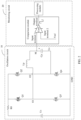
- FIG. 1 is a schematic diagram of a structure of a wireless charging circuit according to an embodiment of this application.
- the circuit includes an oscillation circuit 10 and a monitoring circuit 20.
- the oscillation circuit 10 includes a power supply 1001, a detection and control circuit 1002, and an LC series circuit 1003 that are sequentially connected.
- the monitoring circuit 20 includes a comparison module 2001 and a processing module 2002.
- the power supply 1001 may be an excitation voltage source Us, and is configured to provide a voltage for the oscillation circuit 10.
- the detection and control circuit 1002 is connected in series to the power supply 1001 and the LC series circuit 1003, and is configured to detect a voltage and control charging and discharging of the LC series circuit 1003.
- the detection and control circuit 1002 includes at least one switching transistor.
- the switching transistor includes a switch, a diode, a metal-oxide-semiconductor field-effect transistor (MOSFET transistor), an insulated gate bipolar transistor (Insulated Gate Bipolar Transistor, IGBT), and the like, or the switching transistor may further include another material.
- the LC series circuit 1003 outputs a resonant voltage signal in a damped oscillation process, and the resonant voltage signal is output to the comparison module 2001 and the processing module 2002.
- the comparison module 2001 and the processing module 2002 perform sampling processing on the resonant voltage signal, calculate a Q value, and monitor a foreign object by using the Q value.
- circuit components in the wireless charging circuit may include the following specific implementations.
- FIG. 2 is a schematic diagram of a structure of another wireless charging circuit according to an embodiment.
- the circuit includes an oscillation circuit 10 and a monitoring circuit 20.
- the oscillation circuit 10 is connected to the monitoring circuit 20.
- the oscillation circuit 10 includes an excitation voltage source Us, a full-bridge circuit, an LC series circuit, and an equivalent impedance R of the LC series circuit.
- the equivalent impedance R is not shown in FIG. 2 .
- a voltage amplitude of the excitation voltage source Us is U 0 .
- the wireless charging circuit further includes a charging control resistor R0.
- the resistor R0 is configured to suppress oscillation of the circuit oscillation 10 when the LC series circuit is charged.
- the full-bridge circuit includes a first bridge arm 11 and a second bridge arm 12 that are connected in parallel.
- the first bridge arm 11 includes a first switching transistor Q1 and a third switching transistor Q3.
- the second bridge arm 12 includes a second switching transistor Q2 and a fourth switching transistor Q4.
- Q1 is connected in series to Q3, and Q2 is connected in series to Q4.
- a phase midpoint of the first bridge arm 11 is O1
- a phase midpoint of the second bridge arm 12 is O2. Electric potentials at two terminals of the phase midpoint of each bridge arm are equal.
- One terminal of the full-bridge circuit is connected to a positive electrode of the excitation voltage source Us through the charging control resistor R0, and the other terminal is connected to a negative electrode of the excitation voltage source Us.
- the excitation voltage source Us is configured to provide a stable voltage for the LC series circuit.
- the full-bridge circuit may be configured to control the excitation voltage source Us to charge the LC series circuit and control the LC series circuit to discharge.
- the LC series circuit includes an inductor Lp and a resonance capacitor Cp that are connected in series.
- the inductor Lp and the resonance capacitor Cp are connected in series.
- a phase midpoint of the inductor Lp and the resonance capacitor Cp is M.
- the LC series circuit further includes the equivalent impedance R. The equivalent impedance is not shown in FIG. 2 .
- the LC series circuit is connected to the full-bridge circuit. Specifically, the phase midpoint O1 of the first bridge arm of the full-bridge circuit is connected to one terminal of the LC series circuit, and the phase midpoint O2 of the second bridge arm of the full-bridge circuit is connected to the other terminal of the LC series circuit.
- a voltage of the phase midpoint M of the LC series circuit to ground (GND) is Uc.
- a pin that is output at the phase midpoint M is connected to the monitoring circuit 20.
- the monitoring circuit 20 includes a comparison module and a processing module.
- the comparison module includes a comparator.
- the comparator may be represented by "Com”.
- the comparator Com is a voltage comparator.
- the comparison module in this embodiment is described in an example of the comparator Com.
- the comparator includes a first input terminal (also referred to as an input terminal 1), a second input terminal (also referred to as an input terminal 2), and an output terminal.
- the input terminal 1 is a non-inverting input terminal +, and the input terminal 2 is an inverting input terminal -.
- the input terminal 1 is connected to the pin that is output at the phase midpoint M of the LC series circuit.
- the input terminal 2 is connected to a reference power supply.
- the reference power supply provides a reference voltage.
- the output terminal of the comparator is connected to the processing module.
- the reference voltage may be represented as "Vref".
- the reference voltage may be a positive value or a negative value.
- the comparator is configured to obtain a resonant voltage signal that is output when damped oscillation occurs in the oscillation circuit, convert the resonant voltage signal (namely, the voltage Uc of the phase midpoint M of the LC series circuit to ground) into a digital square wave signal, and transmit the digital square wave signal to the processing module.
- the processing module is connected to the output terminal of the comparator, and is configured to receive the digital square wave signal output by the comparator, obtain a resonant voltage attenuation waveform during damped oscillation based on turn-on and turn-off of the switching transistors Q1 to Q4, obtain a first parameter that meets a first preset condition and that is in the resonant voltage attenuation waveform, determine a quality factor Q based on the first parameter, and monitor a foreign object based on the quality factor Q to obtain a monitoring result.
- the quality factor Q represents a ratio of power stored in the oscillation circuit to a power loss in each cycle. A larger Q value indicates a smaller loss and better charging effect.
- the first preset condition is that in each oscillation cycle, a resonant voltage generated during damped oscillation is greater than the reference voltage.
- the voltage of the phase midpoint M of the LC series circuit to ground reaches an amplitude voltage of the excitation voltage source Us, the damped oscillation occurs in the oscillation circuit to generate the resonant voltage.
- the first parameter includes a quantity of peaks, a quantity of troughs, or a sum of the quantity of peaks and the quantity of troughs.
- the first parameter may further include other parameters. Specifically, there are the following three implementations.
- the first parameter is the quantity of peaks.
- the method includes the following steps.
- the processing module obtains the quantity of peaks that meets the first preset condition.
- the quantity of peaks is represented as "n1".
- step 401 includes the following steps.
- the first switching transistor Q1 of the first bridge arm is controlled to be turned off and the third switching transistor Q3 is controlled to be turned on.
- the second switching transistor Q2 of the second bridge arm is controlled to be turned on and the fourth switching transistor Q4 is controlled to be turned off.
- the oscillation circuit forms a first loop: Us ⁇ Q2 ⁇ Cp ⁇ Lp ⁇ Q3 ⁇ Ground (GND)-Us, and the excitation voltage source Us charges the capacitor Cp.
- the oscillation circuit forms a second loop: GND ⁇ Q3 ⁇ Lp ⁇ Cp ⁇ Q4 ⁇ GND, and the capacitor Cp of the LC series circuit discharges.
- FIG. 5a An equivalent circuit is shown in FIG. 5a .
- Controlling Q3 to be turned on, Q4 to be turned on, and Q2 to be turned off is equivalent to thumbing a switch K of the equivalent circuit from a contact a to a contact b (t > 0) to form the second loop.
- the LC series circuit outputs the resonant voltage Uc to the comparator. The resonant voltage starts to attenuate from the amplitude voltage U 0 .
- Step 4011 and step 4012 may be performed by a control circuit connected to the switching transistors Q1 to Q4.
- the switching transistors Q1 to Q4 are all MOSFET transistors, and the control circuit is connected to a gate of each MOSFET transistor and configured to drive the switching transistors Q1 to Q4 to be turned on or off.
- the comparator obtains the resonant voltage signal Uc output by the oscillation circuit, converts the resonant voltage signal Uc into a digital square wave signal, and transmits the digital square wave signal to the processing module.
- the comparator is configured to compare a value of the resonant voltage signal output by the oscillation circuit in each oscillation cycle with a value of the reference voltage. Whether the resonant voltage Uc generated during damped oscillation is greater than the reference voltage Vref in each oscillation cycle is further determined. If yes, the first preset condition is met; otherwise, the first preset condition is not met.
- FIG. 5b is a schematic diagram of the attenuation waveform of the resonant voltage generated by the oscillation circuit.
- the excitation voltage source Us generates a first-order step excitation signal e(t). After the attenuation waveform of the resonant voltage output by the oscillation circuit of the excitation voltage source Us passes through the comparator, the output resonant voltage Uc gradually attenuates within a specific time.
- a wavy line represents a resonant voltage attenuation curve, and a square wave line represents the digital square wave signal obtained through the conversion.
- a frequency of the oscillation cycles is f1.
- Vref is a direct current level.
- the direct current level is a positive level
- a square wave signal is generated, and a rising edge of a square wave appears.
- a start moment of the rising edge is an intersection point of the resonant voltage attenuation curve and the reference voltage. If Uc ⁇ Vref, no square wave signal is generated, and the damped oscillation tends to end.
- a quantity of peaks that meets the first preset condition and that is in the resonant voltage attenuation curve is the same as a quantity of rising edges in the square wave.
- the processing module receives the digital square wave signal from the comparator, obtains the resonant voltage attenuation waveform during damped oscillation based on the turn-on and turn-off of the switching transistors Q1 to Q4, and obtains a quantity n1 of peaks that meets the first preset condition and that is in the resonant voltage attenuation waveform.
- the processing module determines the quantity n1 of peaks based on the digital square wave signal output by the comparator, where n1 is the same as the quantity of rising edges in the square wave.
- n1 is the same as the quantity of rising edges in the square wave.
- the first parameter is the quantity of troughs.
- the method includes the following steps.
- the processing module obtains the quantity of troughs that meets the first preset condition.
- the quantity of troughs is represented as "n2".
- a method for obtaining the quantity n2 of troughs is similar to a method for obtaining the quantity n1 of peaks in step 401.
- the method specifically includes the following steps.
- the first switching transistor Q1 of the first bridge arm is controlled to be turned on and the third switching transistor Q3 is controlled to be turned off.
- the second switching transistor Q2 of the second bridge arm is controlled to be turned off and the fourth switching transistor Q4 is controlled to be turned on.
- the oscillation circuit forms a third loop: Us ⁇ Q1 ⁇ Lp ⁇ Cp ⁇ Q4 ⁇ GND ⁇ Us, and the excitation voltage source Us charges the capacitor Cp.
- FIG. 6a An equivalent circuit is shown in FIG. 6a . Controlling Q3 to be turned on, Q4 to be turned on, Q1 to be turned off, and Q2 to be turned off is equivalent to thumbing a switch K of the equivalent circuit from a contact a to a contact b (t > 0) to form the fourth loop.
- the LC series circuit outputs the resonant voltage signal Uc to the comparator.
- the comparator obtains the resonant voltage signal Uc output by the oscillation circuit, converts the resonant voltage signal Uc into a digital square wave signal, and transmits the digital square wave signal to the processing module.
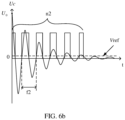
- FIG. 6b is a schematic diagram of the attenuation waveform of the resonant voltage output by the oscillation circuit.
- the excitation voltage source Us generates a first-order step excitation signal e(t). After an attenuation oscillation signal of the LC oscillation circuit of the excitation voltage source Us passes through the voltage comparator, the output voltage gradually attenuates within a specific time.
- a wavy line represents a curve of the resonant voltage attenuation waveform, this waveform and the waveform shown in FIG.
- a frequency of the oscillation cycles is f2.
- Uc resonant voltage
- Vref resonant voltage
- Uc resonant voltage
- Vref resonant voltage
- no square wave signal is generated, and the damped oscillation tends to end.
- a quantity of peaks that meets the first preset condition and that is in the waveform shown in FIG. 6b is equivalent to a quantity of troughs in the attenuation waveform shown in FIG. 5b .
- the quantity of troughs is the same as a quantity of rising edges in the square wave.
- the processing module receives the digital square wave signal from the comparator, and determines the quantity n2 of troughs based on the digital square wave signal.
- the quantity of troughs that meets the first preset condition is 6.
- n2 6.
- the corresponding oscillation frequency is f2.
- the first parameter is the sum of the quantity of peaks and the quantity of troughs.
- the method includes the following steps.
- the processing module obtains the sum of the quantity of peaks and the quantity of troughs.
- the sum (or referred to as a total quantity) may be represented as n.
- n n1 + n2
- the oscillation frequency is f ⁇ f1 ⁇ f2.
- the first parameter may further include a process of obtaining these parameters.
- the processing module determines the quality factor Q based on the sum n (the first parameter) of the quantity of peaks and the quantity of troughs.
- an input source of the LC series circuit is the excitation voltage source Us
- an output direct current voltage amplitude of the excitation voltage source Us is U 0
- a voltage of the fully charged capacitor Cp is U 0 .
- u t ⁇ 1 n U 0 ⁇ e ⁇ ⁇ 0 2 Q t .
- u ( t ) is a negative peak value.
- u ( t ) is a positive peak value.
- Peak or trough voltages corresponding to any two peak moments t1 and t2 are selected as U1 and U2, where t1 and t2 are moments of any two peaks or troughs in the resonant voltage attenuation waveform.
- t1 is a peak moment of the oscillation waveform, and t2 is another peak moment of the oscillation waveform; t1 is a peak moment of the oscillation waveform, and t2 is a trough moment of the oscillation waveform; t1 is a trough moment of the oscillation waveform, and t2 is another peak moment of the oscillation waveform; or t1 is a trough moment of the oscillation waveform, and t2 is another trough moment of the oscillation waveform.
- the processing module monitors the foreign object based on the quality factor Q to obtain the monitoring result.
- a monitoring method is setting two thresholds: a first threshold and a second threshold.
- the first threshold is less than the second threshold.
- the monitoring result is obtained based on the Q value obtained in the foregoing step when the following condition is met.
- the quality factor Q is less than or equal to the first threshold, it is determined that the foreign object exists in a wireless charging coil.
- the quality factor Q is greater than the first threshold, and is less than or equal to the second threshold, it is determined that the foreign object may exist in a wireless charging coil and needs to be further inspected.
- the quality factor Q is greater than the second threshold, it is determined that no foreign object exists in a wireless charging coil.
- the first parameter includes the quantity n1 of peaks or the quantity n2 of troughs.
- m 1.
- the first parameter includes the sum of the quantity of peaks and the quantity of troughs.
- n n1 + n2.
- m 2.
- accuracy of Q is limited by a step value k.
- a smaller value of k indicates a larger value of m and higher accuracy of Q.
- the value of m is 2.
- this case doubles a quantity of sampled peaks, and halves a measurement step unit under the specific Q value, to double accuracy of the Q value and enhance a capability of identifying the foreign object.
- possible measurement accuracy is 1.
- obtained measurement accuracy is 0.5.
- the measurement step unit of the Q value is changed from an original integer to half of the integer. Because the step unit is reduced, a measurement result is more accurate, and whether the foreign object exists in the coil can be more accurately determined, to improve measurement accuracy.
- the first parameter may further include other parameters, so that the value of m is greater than 2, to obtain the smaller measurement accuracy unit and the more accurate measurement result.
- the full-bridge circuit outputs the output voltage of the LC series circuit, and calculates the Q value based on the quantity of peaks, the quantity of troughs, or the sum of the quantity of peaks and the quantity of troughs, to monitor the foreign object in the charging coil.
- This embodiment provides another wireless charging circuit.
- the wireless charging circuit is similar to Embodiment 1 in structure except that in this embodiment, the full-bridge circuit of the oscillation circuit 10 is replaced with a half-bridge circuit, and a voltage biasing module is added to the monitoring circuit.
- the comparison module includes two or more comparators. Further, the two or more comparators are also referred to as integrated voltage comparators.
- the wireless charging circuit includes an oscillation circuit 10 and a monitoring circuit 20.
- the oscillation circuit 10 includes an excitation voltage source Us, the half-bridge circuit, an LC series circuit, and an equivalent impedance R of the LC series circuit.
- the equivalent resistance R is not shown in FIG. 7 .
- U 0 is a voltage amplitude of the excitation voltage source Us with a variable frequency.
- the wireless charging circuit further includes a charging control resistor R0 configured to suppress oscillation of the circuit oscillation 10 when the LC series circuit is charged.
- the half-bridge circuit includes a fifth switching transistor Q5 and a sixth switching transistor Q6.
- Q5 is connected in series to Q6.
- a phase midpoint of the half-bridge circuit is O3.
- One terminal of the half-bridge circuit is connected to the charging control resistor R0, and the other terminal is connected to a negative electrode of the excitation voltage source Us.
- the LC series circuit includes an inductor Lp and a resonance capacitor Cp.
- a phase midpoint of the inductor Lp and the resonance capacitor Cp is M.
- the LC series circuit further includes the equivalent impedance R.
- the phase midpoint M of the LC series circuit is connected to the monitoring circuit 20, and is configured to output a resonant voltage signal generated during damped oscillation to the monitoring circuit 20.
- the resonant voltage signal is also referred to as a voltage of the phase midpoint M of the LC series circuit to ground.
- the monitoring circuit 20 includes a voltage biasing module, a comparison module, and a processing module.
- the voltage biasing module is connected to the oscillation circuit, and is configured to receive the resonant voltage signal output by the oscillation circuit, bias the resonant voltage signal, and transmit a biased resonant voltage signal to the comparison module.
- the comparison module is configured to receive the biased resonant voltage signal, convert the output biased resonant voltage signal into a digital square wave signal, and output the digital square wave signal to the processing module.
- a biased resonant voltage Uc + V ref 0 is output, where V ref 0 is a bias voltage.
- An output terminal of the comparison module is connected to the processing module. Further, the comparison module includes a first comparator (which may be represented as "Com1”) and a second comparator (which may be represented as "Com2").
- Com1 includes an input terminal d1, an input terminal d2, and an output terminal h1.
- Com2 includes an input terminal g1, an input terminal g2, and an output terminal h2.
- the phase midpoint M of the LC series circuit is connected to the input terminal d2 of Com1 and the input terminal g1 of Com2 through the voltage biasing module.
- the input terminal d1 is connected to a first voltage source.
- the input terminal g2 is connected to a second voltage source.
- the output terminal h1 of Com1 is connected to the output terminal h2 of Com2, and a connection point is P.
- the first voltage source is configured to provide a first reference voltage V ref 1 for Com1.
- the second voltage source is configured to provide a second reference voltage V ref 2 for Com2.
- the input terminals d1 and g1 are non-inverting input terminals +, and the input terminals d2 and g2 are inverting input terminals -.
- the comparison module is configured to determine whether the biased resonant voltage UC + V ref 0 is between the first reference voltage V ref 1 and the second reference voltage V ref 2 . If yes, V ref 2 ⁇ Uc + V ref 0 ⁇ V ref 1 . In this case, an output voltage is a low level. Otherwise, the output voltage is a high level. A square wave signal is generated when the high level is output, and a rising edge is formed.
- the comparison module transmits the generated digital square wave signal to the processing module.
- the damped oscillation occurs in the oscillation circuit to generate a resonant voltage.
- the resonant voltage is biased by the voltage biasing module to obtain the resonant voltage Uc + V ref 0 , where Uc is the resonant voltage generated during damped oscillation, and V ref 0 is the bias voltage.
- a second preset condition is Uc + V ref 0 > V ref 1 or Uc + V ref 0 ⁇ V ref 2 , where V ref 1 is the first reference voltage, and V ref 2 is the second reference voltage.
- the processing module receives the digital square wave signal output by the comparison module, obtains a resonant voltage attenuation waveform during damped oscillation based on turn-on and turn-off of switching transistors Q1 to Q4, obtains a second parameter that meets the second preset condition and that is in the resonant voltage attenuation waveform, determines a Q value based on the second parameter, and monitors a foreign object based on a quality factor Q to obtain a monitoring result.
- the second parameter includes a sum of a quantity of peaks and a quantity of troughs.
- a method for determining, by the processing module, the Q value based on the second parameter includes the following steps.
- the oscillation circuit 802 When the voltage of the phase center M of the LC series circuit to ground is increased to the amplitude voltage U 0 , control Q5 to be turned off and Q6 to be turned on.
- the oscillation circuit forms a sixth loop: GND ⁇ Q6 ⁇ Lp ⁇ Cp ⁇ GND, and the capacitor Cp of the LC series circuit discharges, so that the oscillation circuit starts to perform the damped oscillation and outputs the resonant voltage signal Uc.
- the resonant voltage signal Uc starts to attenuate from U 0 .
- An equivalent circuit is shown in FIG. 5a .
- the LC series circuit outputs the resonant voltage signal Uc to the voltage biasing module of the monitoring circuit.
- the voltage biasing module receives the resonant voltage signal output by the oscillation circuit, biases the resonant voltage signal, and transmits a biased resonant voltage signal to the comparison module.
- the comparison module receives the biased resonant voltage signal, converts the biased resonant voltage signal into a digital square wave signal, and outputs the digital square wave signal to the processing module.
- the processing module receives the digital square wave signal, obtains the resonant voltage attenuation waveform during damped oscillation based on the turn-on and turn-off of the switching transistors Q1 to Q4, and obtains the second parameter that meets the second preset condition and that is in the resonant voltage attenuation waveform.
- the second parameter includes the sum of the quantity of peaks and the quantity of troughs.
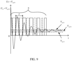
- FIG. 9 is a schematic diagram of an attenuation waveform of a resonant voltage Uc in an oscillation circuit.
- V ref 0 is the bias voltage
- V ref 1 is the first reference voltage
- V ref 2 is the second reference voltage
- U 0 + V ref 0 represents a voltage that is output after the amplitude voltage U 0 generated by the oscillation circuit is processed by using the bias voltage V ref 0 .
- Uc is the voltage of the phase midpoint M of the LC series circuit to ground, and is also referred to as the resonant voltage.
- a maximum amplitude of the resonant voltage is U 0 .
- the processing module determines the quality factor Q based on the second parameter (the sum of the quantity of peaks and the quantity of troughs).
- the processing module monitors the foreign object based on the quality factor Q to obtain the monitoring result.
- a method for determining, by the processing module based on the Q value, whether the foreign object exists in a wireless charging coil is the same as that in Embodiment 1. Details are not described herein again in this embodiment.
- the wireless charging circuit provided in this embodiment monitors the sum of the quantity of peaks and the quantity of troughs in the half cycle by using the comparison module, to calculate the Q value.
- this case halves a measurement step unit. Because the step unit is smaller, a measurement result is more accurate, and whether the foreign object exists in the coil can be more accurately determined, to double monitoring accuracy of the Q value and enhance a capability of identifying the foreign object.
- the inductor Lp and the resonance capacitor Cp of the LC series circuit switch their positions.
- an attenuation waveform of a damped oscillation voltage generated during damped oscillation is transmitted.
- the biased resonant voltage Uc + V ref 0 starts to attenuate from -( U 0 - V ref 0 ) in an oscillation manner. If Uc + V ref 0 > V ref 1 , a high level is output, and a rising edge is generated. A start moment of the rising edge is an intersection point of the biased resonant voltage and the first reference voltage V ref 1 .
- FIG. 10 the inductor Lp and the resonance capacitor Cp of the LC series circuit switch their positions. In this case, an attenuation waveform of a damped oscillation voltage generated during damped oscillation is transmitted.
- the biased resonant voltage Uc + V ref 0 starts to attenuate from -( U 0 - V ref 0 ) in an oscillation manner. If Uc + V ref
- a square wave signal with a solid line is generated. If UC + V ref 0 ⁇ V ref 2 , a high level is output. In this case, the second preset condition is met, and a rising edge is generated. A start moment of the rising edge is an intersection point of the biased resonant voltage and the second reference voltage V ref 2 . As shown in FIG. 11 , a square wave signal with a dashed line is generated. If V ref 2 ⁇ Uc+V ref 0 ⁇ V ref 1 , the second preset condition is not met, a high level is not generated, and a low level signal is output.
- the processing module in the foregoing embodiment may be a processing chip or a processing apparatus. As shown in FIG. 12 , the processing module includes a processor 1201 and a memory 1202. The processor 1201 is coupled to the memory 1202. In addition, the processing module may further include more or fewer components, or combine some components, or have different component arrangements. This is not limited in this application.
- the processor 1201 is a control center of the processing module, is connected to all parts of the entire apparatus through various interfaces and lines, and runs or executes a software program or module stored in the memory 1202 and invokes data stored in the memory 1202 to implement a corresponding function.
- the processor 1201 may include an integrated circuit (integrated circuit, IC), for example, may include a single packaged IC, or may include a plurality of packaged ICs that are connected and that have a same function or different functions.
- the processor 1201 may include a central processing unit (central processing unit, CPU) and the like.
- the memory 1202 may include a volatile memory (volatile memory), for example, a random access memory (random access memory, RAM); and may further include a non-volatile memory (non-volatile memory), for example, a flash memory (flash memory), a hard disk drive (hard disk drive, HDD), or a solid-state drive (solid-state drive, SSD).
- volatile memory volatile memory
- non-volatile memory non-volatile memory
- flash memory flash memory
- HDD hard disk drive
- solid-state drive solid-state drive
- SSD solid-state drive
- the memory 1202 may further include a combination of the foregoing types of memories.
- the memory may store a program, code, or data.
- this application further provides a computer storage medium.
- the computer storage medium may store programs. When the programs are executed, some or all of the steps of the method for determining the Q value provided in this application and embodiments shown in FIG. 4a , FIG. 4b , and FIG. 8 may be included.
- the storage medium may be a magnetic disk, an optical disc, a read-only memory (ROM), a random access memory (RAM), or the like.
- the computer program product includes one or more computer instructions, such as computation instructions.
- a computer loads and executes the computer program, all or some of the procedures or functions are generated according to embodiments of this application.
- the computer may be a general-purpose computer, a dedicated computer, a computer network, or another programmable apparatus.
- the computer instructions may be stored in a computer-readable storage medium.
- the computer-readable storage medium may be any usable medium accessible by a computer, or a storage device, such as a server or a data center, integrating one or more usable media.
- the usable medium may be a magnetic medium, for example, a floppy disk, a hard disk, a magnetic tape, an optical medium (for example, a DVD), a semiconductor medium, for example, a solid-state drive (SSD), or the like.
- a wireless charging device provided in this application includes but is not limited to the circuit structure of the wireless charging circuit in Embodiment 1 and Embodiment 2.
- the processing module of the wireless charging circuit may be the processing chip or the processing apparatus shown in FIG. 12 , and is configured to perform the method for determining the Q value in FIG. 4a , FIG. 4b , or FIG. 8 .
- the method for determining the Q value in embodiments of this application may be applied to a transmit terminal device and may also be applied to a receive terminal device.
- a to-be-charged device is a mobile phone.
- the method for determining the Q value and the method for monitoring the foreign object are used for monitoring a wireless charging environment of the mobile phone, and may also be used for monitoring another charging environment, for example, vehicle-mounted charging.
- An embodiment of this application further provides a wireless charging system.
- the system includes a transmit device and a receive device.
- the transmit device is the wireless charging device in the foregoing embodiment.
- the receive device is a to-be-charged device.
- the wireless charging device includes the wireless charging circuit in Embodiment 1 or Embodiment 2, and is configured to implement the method for determining the Q value in embodiments of this application and monitor a foreign object in a wireless charging coil.
- the transmit device is the wireless charging device.
- the receive device is the to-be-charged device.
- the receive device further includes the wireless charging circuit in Embodiment 1 or Embodiment 2, is configured to implement the method for determining the Q value in embodiments of this application, and has a function of monitoring the foreign object in the wireless charging coil.
- the receive device includes an oscillation circuit and a monitoring circuit that are sequentially connected.
- the oscillation circuit includes an excitation voltage source, a full-bridge circuit, and an LC series circuit that are connected in series.
- the excitation voltage source is configured to provide a stable voltage for the LC series circuit.
- the full-bridge circuit includes a first bridge arm and a second bridge arm that are connected in parallel.
- the first bridge arm includes a first switching transistor Q1 and a third switching transistor Q3.
- the second bridge arm includes a second switching transistor Q2 and a fourth switching transistor Q4.
- the LC series circuit includes an inductor and a resonance capacitor that are connected in series. One terminal of the LC series circuit is connected to a phase midpoint of the first bridge arm, and the other terminal is connected to a phase midpoint of the second bridge arm.
- a phase midpoint of the LC series circuit is connected to the monitoring circuit, and is configured to output a resonant voltage signal during damped oscillation to the monitoring circuit.
- the monitoring circuit includes a comparison module and a processing module.
- the comparison module is configured to receive the resonant voltage signal, and convert the resonant voltage signal into a digital square wave signal.
- the processing module is configured to receive the digital square wave signal, obtain a resonant voltage attenuation waveform during damped oscillation based on turn-on and turn-off of the switching transistors Q1 to Q4, obtain a first parameter that meets a first preset condition and that is in the resonant voltage attenuation waveform, and determine a quality factor Q based on the first parameter.
- the first parameter includes a quantity of peaks, a quantity of troughs, or a sum of the quantity of peaks and the quantity of troughs.
- the processing module is further configured to monitor the foreign object based on the quality factor Q to obtain a monitoring result. If the quality factor Q is less than or equal to a first threshold, it is determined that the foreign object exists. If the quality factor Q is greater than a first threshold and less than or equal to a second threshold, it is determined that the foreign object may exist. If the quality factor Q is greater than a second threshold, it is determined that no foreign object exists.
- Embodiment 2 and embodiments of the receive device are basically similar to a method embodiment, and therefore are described briefly.
- related parts refer to descriptions in the method embodiment.
Landscapes
- Engineering & Computer Science (AREA)
- Power Engineering (AREA)
- Computer Networks & Wireless Communication (AREA)
- Physics & Mathematics (AREA)
- Electromagnetism (AREA)
- Charge And Discharge Circuits For Batteries Or The Like (AREA)
- Secondary Cells (AREA)
Description
- This application relates to the field of wireless charging technologies, and in particular, to wireless charging circuits, a wireless charging method, a device, and a wireless charging system.
- Wireless charging refers to a process in which a device that is charged based on an electromagnetic wave induction principle. The principle is similar to that of a transformer. There is a coil at a transmit terminal and a coil at a receive terminal. The coil at the transmit terminal is connected to a wired power supply and generates an electromagnetic signal. The coil at the receive terminal induces the electromagnetic signal from the transmit terminal, and converts the electromagnetic signal into a required direct current, to charge a battery at the receive terminal.
- The Qi standard is a "wireless charging" standard launched by the Wireless Power Consortium (Wireless Power Consortium, WPC), and has two features: convenience and universality. With development and popularization of wireless charging technologies, many wireless charging products emerge in the market. In particular, wireless charging products based on the Qi standard of the WPC have a large market share.
- When wireless charging is performed on the receive terminal such as a mobile phone, the transmit terminal needs to monitor and identify the receive terminal in real time. When identifying the receive terminal, the transmit terminal starts to transmit power in the wireless charging coil. In addition, a charging environment in the wireless charging coil also needs to be monitored. If there is a foreign object in the coil, for example, a bank card, an identity card, or another metal foreign object, a magnetic field generates an eddy current, and these foreign objects consume power in the wireless charging coil. This reduces charging efficiency, and also causes an accident such as a fire. Therefore, foreign object monitoring becomes a primary problem to ensure safety in a wireless charging process.
-
US 2019/199142 describes a method for performing foreign object detection for a wireless power transmitter in which a matching network and transmit coil are energized, and a resonance is excited. The resonance is allowed to decay. A temporal characteristic of the decay is measured. The temporal characteristic is analyzed to determine whether a foreign object is coupled to an electromagnetic field generated by the transmit coil. -
US 2015/285926 describes a wireless power transmitter that includes an analog-to-digital converter (ADC) and a controller. The ADC is configured to convert an analog signal associated with a power train to digital values. The controller is configured to cause pulses to be applied to the power train to thereby cause the power train to ring, receive digital values from the ADC acquired while the power train is ringing and after the pulses complete, and, based on an analysis of the digital values of the ringing of the power train, to determine whether a wireless power receiver is present on or near the wireless power transmitter or whether a foreign object is present on the transmitter. -
US 2010/013321 describes a power receiving control device provided to a power receiving device included in a contactless power transmission system that transmits electric power from a power transmission device to the power receiving device by electromagnetically coupling a primary coil and a secondary coil so as to feed the electric power to a load serving as a power feeding object from a voltage output node of the power receiving device, - This application provides a wireless charging circuit and a wireless charging method. The wireless charging circuit can monitor a foreign object more accurately by using a Q value. Specifically, this application discloses the following technical solutions. The scope of protection of the present invention is set out by the appended claims.
- According to a first aspect, an embodiment of this application provides a wireless charging circuit. The circuit includes an oscillation circuit and a monitoring circuit that are sequentially connected. The oscillation circuit includes an excitation voltage source Us, a full-bridge circuit, and an LC series circuit that are connected in series. The excitation voltage source Us is configured to provide a stable voltage for the LC series circuit.
- Further, the full-bridge circuit includes a first bridge arm and a second bridge arm that are connected in parallel. The first bridge arm includes a first switching transistor Q1 and a third switching transistor Q3. The second bridge arm includes a second switching transistor Q2 and a fourth switching transistor Q4. The LC series circuit includes an inductor Lp and a resonance capacitor Cp that are connected in series. One terminal of the LC series circuit is connected to a phase midpoint of the first bridge arm, and the other terminal is connected to a phase midpoint of the second bridge arm. A phase center of the LC series circuit is connected to the monitoring circuit, and is configured to output a resonant voltage signal during damped oscillation to the monitoring circuit.
- The monitoring circuit includes a comparison module and a processing module. The comparison module is configured to receive the resonant voltage signal output by the oscillation circuit, and convert the resonant voltage signal into a digital square wave signal. The processing module is configured to: receive the digital square wave signal, obtain a resonant voltage attenuation waveform during damped oscillation based on turn-on and turn-off of the switching transistors Q1 to Q4, obtain a first parameter that meets a first preset condition and that is in the resonant voltage attenuation waveform, and determine a quality factor Q based on the first parameter. The first parameter includes a quantity of peaks, a quantity of troughs, or a sum of the quantity of peaks and the quantity of troughs.
- In addition, the processing module is further configured to monitor a foreign object based on the quality factor Q to obtain a monitoring result. The quality factor Q represents a ratio of power stored in the oscillation circuit to a power loss in each cycle. A larger Q value indicates a smaller loss of this charging circuit in a same cycle and better performance.
- According to the wireless charging circuit provided in this embodiment, in a design of the full-bridge circuit including the first bridge arm and the second bridge arm, turn-on and turn-off of the switching transistors in the full-bridge circuit are controlled, to implement charging and discharging of the oscillation circuit. In addition, the monitoring circuit determines, based on the waveform of the resonant voltage output by the oscillation circuit, the quantity of peaks, the quantity of troughs, or the sum of the quantity of peaks and the quantity of troughs that meets the preset condition, and calculates the quality factor Q, to monitor the foreign object by using the Q value.
- The comparison module includes a comparator. Further, the comparator is a voltage comparator. One input terminal of the voltage comparator is connected to a reference power supply and is configured to obtain a reference voltage, and the other input terminal is connected to an output terminal of the oscillation circuit and is configured to receive a resonant voltage generated by the oscillation circuit. An output terminal of the comparator is connected to the processing module.
- In addition, the comparator may alternatively be replaced with another circuit, for example, an operational amplifier. The comparison module may further include another auxiliary control circuit. This is not limited in this embodiment.
- In the first aspect, the first preset condition is that in each oscillation cycle, the resonant voltage generated during damped oscillation is greater than the reference voltage. When a voltage of the phase midpoint of the LC series circuit to ground reaches an amplitude voltage of the excitation voltage source Us, the damped oscillation occurs in the oscillation circuit to generate the resonant voltage.
- Further, in a specific implementation of the first aspect, there may be the following three possible implementations for the first parameter.
- In a first possible implementation, the first parameter includes the quantity of peaks. The quantity of peaks that meets the first preset condition is the quantity of peaks that meets the first preset condition and that is determined, based on the digital square wave signal output by the comparison module, by the processing module when the first switching transistor Q1 of the first bridge arm is off, the third switching transistor Q3 of the first bridge arm is on, the second switching transistor Q2 of the second bridge arm is changed from on to off, and the fourth switching transistor Q4 of the second bridge arm is changed from off to on.
- In a second possible implementation, the first parameter includes the quantity of troughs. The quantity of troughs that meets the first preset condition is the quantity of troughs that meets the first preset condition and that is determined, based on the digital square wave signal output by the comparison module, by the processing module when the second switching transistor Q2 of the second bridge arm is off, the fourth switching transistor Q4 of the second bridge arm is on, the first switching transistor Q1 of the first bridge arm is changed from on to off, and the third switching transistor Q3 of the first bridge arm is changed from off to on.
- In a third possible implementation, the first parameter includes the sum of the quantity of peaks and the quantity of troughs. The sum is the sum of the quantity of peaks that meets the first preset condition and the quantity of troughs that meets the first preset condition.
- With reference to the first aspect, in a possible implementation of the first aspect, the processing module is specifically configured to determine, based on the first parameter, the quality factor Q:

m and n are both positive integers, m ≥ 1, and U1 and U2 are any peak voltage or any trough voltage in the resonant voltage attenuation waveform. - Further, when the first parameter is the quantity of peaks or the quantity of troughs and m = 1, the quality factor Q is:
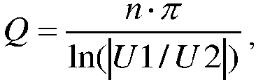
n is the quantity of peaks or the quantity of troughs. - When the first parameter is the sum of the quantity of peaks and the quantity of troughs and m = 2, the quality factor Q is:

n is the sum of the quantity of peaks and the quantity of troughs. - According to the method provided in this embodiment, under the specific Q value, a measurement step unit is determined based on m. A larger value of m indicates a smaller step unit and higher measurement accuracy. When the first parameter is the sum of the quantity of peaks and the quantity of troughs, the value of m is 2. Compared with the case in which the Q value is determined based on either the quantity of peaks or the quantity of troughs, this case halves the measurement step unit, to double accuracy of the Q value and enhance a capability of identifying the foreign object. For example, the turn-on and turn-off of the four switching transistors in the full-bridge circuit are controlled, to change the measurement step unit of the Q value from an original integer to half of the integer. Because the step unit is reduced, a measurement result is more accurate, and whether the foreign object exists in the coil can be more accurately determined, to improve measurement accuracy.
- In the foregoing Q value calculation equation,

when the Q value is specific, n is proportional to m, and n is inversely proportional to 1/m. - In addition,

- t1 is a peak moment of the oscillation waveform, and t2 is another peak moment of the oscillation waveform;
- t1 is a peak moment of the oscillation waveform, and t2 is a trough moment of the oscillation waveform;
- t1 is a trough moment of the oscillation waveform, and t2 is another peak moment of the oscillation waveform; or
- t1 is a trough moment of the oscillation waveform, and t2 is another trough moment of the oscillation waveform.
- The larger value of m indicates the smaller step unit, the higher measurement accuracy, and the more accurate measurement result.
- According to a second aspect, an embodiment of this application further provides another wireless charging circuit. The circuit includes an oscillation circuit and a monitoring circuit that are sequentially connected. The oscillation circuit includes an excitation voltage source Us, a half-bridge circuit, and an LC series circuit that are connected in series. The excitation voltage source Us is configured to provide a stable voltage for the LC series circuit.
- Further, the half-bridge circuit includes a fifth switching transistor Q5 and a sixth switching transistor Q6 that are connected in series. The LC series circuit includes an inductor Lp and a resonance capacitor Cp that are connected in series. One terminal of the LC series circuit is connected to a phase midpoint of the half-bridge circuit, and the other terminal is connected to the ground. A phase center of the LC series circuit is connected to the monitoring circuit, and is configured to output a resonant voltage signal during damped oscillation to the monitoring circuit.
- The monitoring circuit includes a voltage biasing module, a comparison module, and a processing module. The voltage biasing module is connected to the oscillation circuit, and is configured to receive the resonant voltage signal output by the oscillation circuit, bias the resonant voltage signal, and transmit a biased resonant voltage signal to the comparison module. The comparison module receives the biased resonant voltage signal, converts the biased resonant voltage signal into a digital square wave signal, and outputs the digital square wave signal to the processing module. The processing module is configured to: receive the digital square wave signal, obtain a resonant voltage attenuation waveform during damped oscillation based on turn-on and turn-off of the switching transistors Q1 to Q4, obtain a second parameter that meets a second preset condition and that is in the resonant voltage attenuation waveform, and determine a quality factor Q based on the second parameter, where the second parameter includes a sum of a quantity of peaks and a quantity of troughs. The processing module is further configured to monitor a foreign object based on the quality factor Q to obtain a monitoring result. The quality factor Q represents a ratio of power stored in the oscillation circuit to a power loss in each cycle.
- In this aspect, the half-bridge circuit is designed in the oscillation circuit. Turn-on and turn-off of the fifth switching transistor Q5 and the sixth switching transistor Q6 in the half-bridge circuit are controlled, to implement the half-cycle oscillation circuit. The comparison module processes a resonant voltage output by the oscillation circuit to obtain the second parameter and an oscillation frequency, and calculates a Q value, to monitor the foreign object in a wireless charging coil.
- In addition, this circuit can also measure and obtain the sum of the quantity of peaks and the quantity of troughs in a half cycle, to calculate the Q value. Compared with the case in which the voltage comparator is used for calculating the Q value, this case halves a measurement step unit. Because the step unit is smaller, a measurement result is more accurate, and whether the foreign object exists in the coil can be more accurately determined, to double monitoring accuracy of the Q value and enhance a capability of identifying the foreign object.
- The second preset condition is: Uc + V ref0>V ref1or Uc + V ref 0 < V ref 2 , where Uc is a resonant voltage generated during damped oscillation, V ref 0 is a bias voltage, Uc + V ref 0 is a resonant voltage biased by the voltage biasing module, V ref 1 is a first reference voltage, and V ref 2 is a second reference voltage; and when a voltage of the phase midpoint of the LC series circuit to ground reaches an amplitude voltage of the excitation voltage source Us, the damped oscillation occurs in the oscillation circuit to generate the resonant voltage.
- With reference to the second aspect, in a possible implementation of the second aspect, the sum of the quantity of peaks and the quantity of troughs is the sum of the quantity of peaks and the quantity of troughs that meets the second preset condition and that is determined, based on the digital square wave signal output by the comparison module, by the processing module when the fifth switching transistor Q5 is changed from on to off and the sixth switching transistor Q6 is changed from off to on.
- The switching transistors Q5 and Q6 may be controlled by a control circuit connected to the switching transistors Q5 and Q6. For example, both the switching transistors Q5 and Q6 are diodes, MOSFET transistors, IGBTs, or the like, and the control circuit is connected to a gate of each switching transistor and configured to drive the switching transistors Q5 and Q6 to be turned on or off.
- With reference to the second aspect, in a possible implementation of the second aspect, an input terminal of the comparison module is connected to an output terminal of the voltage biasing module, and an output terminal is connected to the processing module.
- The comparison module includes a first comparator and a second comparator. Specifically, the first comparator and the second comparator each include a first input terminal, a second input terminal, and an output terminal. The first input terminal of the first comparator is connected to a first voltage source, and is configured to obtain the first reference voltage provided by the first voltage source. The second input terminal of the first comparator and the first input terminal of the second comparator are connected to each other to be used as the input terminal of the comparison module. The second input terminal of the second comparator is connected to a second voltage source, and is configured to obtain the second reference voltage provided by the second voltage source. The output terminal of the first comparator and the output terminal of the second comparator are connected to each other to be used as the output terminal of the comparison module.
- Optionally, the first reference voltage and the second reference voltage may be positive values, or may be negative values.
- With reference to the second aspect, in another possible implementation of the second aspect, the processing module is specifically configured to determine, based on the second parameter, the quality factor Q:

n and m are both positive integers, m ≥ 1, U0 is a voltage amplitude of the excitation voltage source Us, ΔV is a voltage difference between a bias voltage and a reference voltage, and the reference voltage is the first reference voltage or the second reference voltage. - Further, when m = 2, the quality factor Q is:

n is the sum of the quantity of peaks and the quantity of troughs. - In each half cycle, if Uc + V ref 0 > ΔV and ΔV = V ref 1 - V ref 0 , or if Uc + V ref 0 <ΔV and ΔV = V ref 0 - V ref 2 , the second preset condition is met, a high level is output, and a rising edge is generated, where Uc is the resonant voltage output by the oscillation circuit, ΔV is the voltage difference, ΔV = V ref 1 - V ref 0 - V ref 0 - V ref 2, V ref 0 is the bias voltage, V ref 1 is the first reference voltage, and V ref 2 is the second reference voltage.
- If V ref 2 ≤ Uc + V ref 0 ≤ V ref 1 , the second preset condition is not met, a high level is not generated, and a low level signal is output.
- According to a third aspect, an embodiment of this application further provides a wireless charging method. The method is applied to a wireless charging circuit. This circuit and the wireless charging circuit according to the first aspect have a same structure. Specifically, the wireless charging circuit includes an oscillation circuit and a monitoring circuit that are sequentially connected.
- The oscillation circuit includes an excitation voltage source Us, a full-bridge circuit, and an LC series circuit that are connected in series. The excitation voltage source Us is configured to provide a stable voltage for the LC series circuit. The full-bridge circuit includes a first bridge arm and a second bridge arm that are connected in parallel. The first bridge arm includes a first switching transistor Q1 and a third switching transistor Q3. The second bridge arm includes a second switching transistor Q2 and a fourth switching transistor Q4. The LC series circuit includes an inductor Lp and a resonance capacitor Cp that are connected in series. One terminal of the LC series circuit is connected to a phase midpoint of the first bridge arm, and the other terminal is connected to a phase midpoint of the second bridge arm. A phase midpoint of the LC series circuit is connected to the monitoring circuit, and is configured to output a resonant voltage signal during damped oscillation to the monitoring circuit. The monitoring circuit includes a comparison module and a processing module. The comparison module is configured to receive the resonant voltage signal, and convert the resonant voltage signal into a digital square wave signal.
- The method includes:
The processing module receives the digital square wave signal, where the digital square wave signal is generated by converting the resonant voltage signal. - The processing module obtains a resonant voltage attenuation waveform during damped oscillation based on turn-on and turn-off of the switching transistors Q1 to Q4, and obtains, based on the resonant voltage attenuation waveform, a first parameter that meets a first preset condition, where the first parameter includes a quantity of peaks, a quantity of troughs, or a sum of the quantity of peaks and the quantity of troughs.
- The processing module determines a quality factor Q based on the first parameter.
- The processing module monitors a foreign object based on the quality factor Q to obtain a monitoring result.
- The first preset condition is that in each oscillation cycle, the resonant voltage generated during damped oscillation is greater than the reference voltage. When a voltage of the phase midpoint of the LC series circuit to ground reaches an amplitude voltage of the excitation voltage source Us, the damped oscillation occurs in the oscillation circuit to generate the resonant voltage.
- With reference to the third aspect, in a possible implementation of the third aspect,
- the first parameter includes the quantity of peaks, and the quantity of peaks that meets the first preset condition is the quantity of peaks that meets the first preset condition and that is determined, based on the digital square wave signal output by the comparison module, by the processing module when the first switching transistor Q1 of the first bridge arm is off, the third switching transistor Q3 of the first bridge arm is on, the second switching transistor Q2 of the second bridge arm is changed from on to off, and the fourth switching transistor Q4 of the second bridge arm is changed from off to on;
- the first parameter includes the quantity of troughs, and the quantity of troughs that meets the first preset condition is the quantity of troughs that meets the first preset condition and that is determined, based on the digital square wave signal output by the comparison module, by the processing module when the second switching transistor Q2 of the second bridge arm is off, the fourth switching transistor Q4 of the second bridge arm is on, the first switching transistor Q1 of the first bridge arm is changed from on to off, and the third switching transistor Q3 of the first bridge arm is changed from off to on; or
- the first parameter includes the sum of the quantity of peaks and the quantity of troughs, and the sum is the sum of the quantity of peaks that meets the first preset condition and the quantity of troughs that meets the first preset condition.
- With reference to the third aspect, in another possible implementation of the third aspect, that the processing module determines a quality factor Q based on the first parameter includes: The processing module determines, based on the first parameter, the quality factor Q:

n and m are both positive integers, m ≥ 1, and U1 and U2 are any peak voltage or any trough voltage in the resonant voltage attenuation waveform. - Further, when m = 2, the quality factor Q is:

n is the sum of the quantity of peaks and the quantity of troughs. - In addition, with reference to the third aspect, in still another possible implementation of the third aspect, the monitoring a foreign object includes: if the quality factor Q is less than or equal to a first threshold, determining that the foreign object exists in a wireless charging coil; if the quality factor Q is greater than a first threshold and less than or equal to a second threshold, determining that the foreign object may exist in a wireless charging coil and needs to be further inspected; or if the quality factor Q is greater than a second threshold, determining that no foreign object exists in a wireless charging coil. The first threshold and the second threshold may be set by a user.
- According to a fourth aspect, an embodiment of this application further provides another wireless charging method. The method is applied to a wireless charging circuit. This circuit and the wireless charging circuit according to the second aspect have a same structure. The wireless charging circuit includes an oscillation circuit and a monitoring circuit that are sequentially connected.
- The oscillation circuit includes an excitation voltage source Us, a half-bridge circuit, and an LC series circuit that are connected in series. The excitation voltage source Us is configured to provide a stable voltage for the LC series circuit. The half-bridge circuit includes a fifth switching transistor Q5 and a sixth switching transistor Q6 that are connected in series. The LC series circuit includes an inductor Lp and a resonance capacitor Cp that are connected in series. One terminal of the LC series circuit is connected to a phase midpoint of the half-bridge circuit, and the other terminal is connected to the ground. A phase midpoint of the LC series circuit is connected to the monitoring circuit, and is configured to output a resonant voltage signal during damped oscillation to the monitoring circuit. The monitoring circuit includes a voltage biasing module, a comparison module, and a processing module. The voltage biasing module receives the resonant voltage signal, biases the resonant voltage signal, and transmits a biased resonant voltage signal to the comparison module. The comparison module receives the biased resonant voltage signal, converts the biased resonant voltage signal into a digital square wave signal, and then outputs the digital square wave signal to the processing module.
- The method includes:
The processing module receives the digital square wave signal. - The processing module obtains a resonant voltage attenuation waveform during damped oscillation based on turn-on and turn-off of the switching transistors Q1 to Q4, and obtains a second parameter that meets a second preset condition and that is in the resonant voltage attenuation waveform, where the second parameter includes a sum of a quantity of peaks and a quantity of troughs. The processing module determines a quality factor Q based on the second parameter.
- The processing module is further configured to monitor a foreign object based on the quality factor Q to obtain a monitoring result.
- Further, the second preset condition is UC + V ref 0 > V ref 1 or Uc + V ref 0 < V ref 2, where V ref 1 is a first reference voltage, V ref 2 is a second reference voltage, V ref 0 is a bias voltage, Uc is a resonant voltage generated during damped oscillation, and Uc + V ref 0 is a resonant electricity biased by the voltage biasing module.
- When a voltage of the phase midpoint of the LC series circuit to ground reaches an amplitude voltage of the excitation voltage source Us, the damped oscillation occurs in the oscillation circuit to generate the resonant voltage.
- With reference to the fourth aspect, in a possible implementation of the fourth aspect, the sum of the quantity of peaks and the quantity of troughs is the sum of the quantity of peaks and the quantity of troughs that meets the second preset condition and that is determined, based on the digital square wave signal output by the comparison module, by the processing module when the fifth switching transistor Q5 is changed from on to off and the sixth switching transistor Q6 is changed from off to on.
- With reference to the fourth aspect, in another possible implementation of the fourth aspect, that the processing module determines a quality factor Q based on the second parameter includes: The processing module determines, based on the second parameter, the quality factor Q:

n and m are both positive integers, m ≥ 1, U 0 is a voltage amplitude of the excitation voltage source Us, ΔV is a voltage difference between a bias voltage and a reference voltage, and the reference voltage is the first reference voltage or the second reference voltage. - Further, when m = 2, the quality factor Q is:

n is the sum of the quantity of peaks and the quantity of troughs. - According to a fifth aspect, an embodiment of this application further provides a processing apparatus. The processing apparatus includes a processor and a memory. The processor is coupled to the memory. Further, the processor is configured to: run or execute computer program instructions stored in the memory, and invoke data in the memory, to perform the method in the implementations of the third aspect or the fourth aspect and monitor, based on a Q value, whether a foreign object exists in a charging coil.
- Optionally, the processor is a processing chip or a processing module.
- Optionally, the processor is a random access memory (RAM) or a nonvolatile memory such as a flash memory or a hard disk.
- According to a sixth aspect, an embodiment of this application further provides a device. The device is a transmit device or a receive device. The transmit device or the receive device includes the wireless charging circuit in the first aspect and the implementations of the first aspect. In addition, the wireless charging circuit is used for implementing the method according to the second aspect and the implementations of the second aspect, and monitoring the foreign object.
- Specifically, the monitoring process includes: determining a relationship between the quality factor Q value and both of a first threshold and a second threshold.
- If a quality factor Q is less than or equal to the first threshold, it is determined that the foreign object exists in a wireless charging coil.
- If a quality factor Q is greater than the first threshold, and is less than or equal to the second threshold, it is determined that the foreign object may exist in a wireless charging coil and needs to be further inspected.
- If a quality factor Q is greater than the second threshold, it is determined that no foreign object exists in a wireless charging coil.
- In addition, whether the foreign object exists may alternatively be monitored by using other methods or strategies.
- According to a seventh aspect, an embodiment of this application further provides a wireless charging system. The system includes a transmit device and a receive device. The transmit device includes the wireless charging circuit according to the first aspect or the second aspect. The receive device is a to-be-charged device.
- Optionally, the receive device further includes the wireless charging circuit according to the first aspect or the second aspect, to monitor a foreign object.
- According to an eighth aspect, an embodiment of this application further provides a computer-readable storage medium. The storage medium stores instructions. When the instructions are run on a computer or a processor, the method according to the implementations of the third aspect or the fourth aspect is performed.
- Further, a computer program product is provided. The computer program product includes computer instructions. When the instructions are executed by a computer or a processor, the method according to the implementations of the third aspect or the fourth aspect may be performed.
-
-
FIG. 1 is a schematic diagram of a structure of a wireless charging circuit according to an embodiment of this application; -
FIG. 2 is a schematic diagram of a structure of another wireless charging circuit according to an embodiment of this application; -
FIG. 3 is a schematic diagram of a structure of a full-bridge circuit according to an embodiment of this application; -
FIG. 4a is a flowchart of a method for determining a Q value according to an embodiment of this application; -
FIG. 4b is a flowchart of a method for determining a quantity of peaks according to an embodiment of this application; -
FIG. 5a is an equivalent circuit diagram of a resonant circuit according to an embodiment of this application; -
FIG. 5b is a schematic diagram of an attenuation waveform of a resonant voltage generated by an oscillation circuit according to an embodiment of this application; -
FIG. 6a is an equivalent circuit diagram of another resonant circuit according to an embodiment of this application; -
FIG. 6b is a schematic diagram of another attenuation waveform of a resonant voltage generated by an oscillation circuit according to an embodiment of this application; -
FIG. 7 is a schematic diagram of a structure of another wireless charging circuit according to an embodiment of this application; -
FIG. 8 is a flowchart of another method for determining a Q value according to an embodiment of this application; -
FIG. 9 is a schematic diagram of still another attenuation waveform of a resonant voltage generated by an oscillation circuit according to an embodiment of this application; -
FIG. 10 is a schematic diagram of a structure of still another wireless charging circuit according to an embodiment of this application; -
FIG. 11 is a schematic diagram of still another attenuation waveform of a resonant voltage generated by an oscillation circuit according to an embodiment of this application; and -
FIG. 12 is a schematic diagram of a structure of a processing module according to an embodiment of this application. - To make a person skilled in the art understand the technical solutions in embodiments of this application better, and make the objectives, features, and advantages of embodiments of this application clearer, the following further describes the technical solutions in embodiments of this application in detail with reference to the accompanying drawings.
- First, technical scenarios used in embodiments of this application are described.
- The technical solutions of this application are applied to a scenario of a wireless charging technology. The scenario includes a wireless charging device and a to-be-charged device. The wireless charging device is configured to charge the to-be-charged device capable of being wirelessly charged. For example, the wireless charging device may be a wireless charging mobile power supply, a wireless charging board, a wireless charger, or the like. The to-be-charged device includes an electronic device with a built-in rechargeable battery, such as a mobile phone, a tablet, a notebook computer, an in-vehicle apparatus, or a digital camera.
- The wireless charging device may also be referred to as a transmit device. The to-be-charged device may also be referred to as a receive device.
- Optionally, the wireless charging device includes a housing, a wireless charging coil, a carrying apparatus, and the like. Specifically, a charging surface for carrying the to-be-charged device is disposed on a surface of the housing. Therefore, the to-be-charged device may be placed on the charging surface of the housing. In addition, in this embodiment of this application, a battery and a circuit board are further disposed in the housing. The battery is configured to store electric energy and output the electric energy. A wireless charging circuit is disposed on the circuit board. The wireless charging circuit is electrically connected to the wireless charging coil, and is configured to control a charging and discharging process of the wireless charging device and control an operation state of the entire wireless charging device.
- The wireless charging coil is disposed in the housing, and is configured to convert the electric energy of the battery into magnetic energy for transmission and emission. The carrying apparatus is disposed in the housing, and is configured to carry and fasten the wireless charging coil and protect the wireless charging coil.
- In this embodiment of this application, how to monitor whether a charging environment is good when the to-be-charged device is charged based on an electromagnetic wave induction principle is a technical problem to be mainly resolved. In other words, whether a foreign object that affects charging quality exists in the wireless charging coil is monitored.
- To resolve the technical problem, an embodiment of this application provides a method for determining a quality factor Q (or referred to as a "Q value"). The quality factor represents a ratio of power stored in a power storage device (such as an inductor or a capacitor) or a resonant circuit to a power loss in each cycle. A Q value of a reactance element in a series resonant loop is equal to a ratio of reactance of the reactance element to an equivalent series resistance of the reactance element. In addition, a larger Q value of the element indicates a smaller loss and better performance of a circuit or a network that includes the element. Therefore, the quality factor Q may be used for evaluating a magnitude of a loop loss. Generally, the Q value ranges from dozens to hundreds. In this embodiment of this application, the Q value may be obtained through damped oscillation. Specifically, a wireless charging circuit is designed to obtain a resonant voltage attenuation waveform generated when the damped oscillation occurs in an LC series circuit, to determine the Q value.
- A wireless charging circuit in a wireless charging device is described in detail in the following embodiment.
-
FIG. 1 is a schematic diagram of a structure of a wireless charging circuit according to an embodiment of this application. The circuit includes anoscillation circuit 10 and amonitoring circuit 20. Theoscillation circuit 10 includes apower supply 1001, a detection andcontrol circuit 1002, and anLC series circuit 1003 that are sequentially connected. Themonitoring circuit 20 includes acomparison module 2001 and aprocessing module 2002. - The
power supply 1001 may be an excitation voltage source Us, and is configured to provide a voltage for theoscillation circuit 10. The detection andcontrol circuit 1002 is connected in series to thepower supply 1001 and theLC series circuit 1003, and is configured to detect a voltage and control charging and discharging of theLC series circuit 1003. The detection andcontrol circuit 1002 includes at least one switching transistor. The switching transistor includes a switch, a diode, a metal-oxide-semiconductor field-effect transistor (MOSFET transistor), an insulated gate bipolar transistor (Insulated Gate Bipolar Transistor, IGBT), and the like, or the switching transistor may further include another material. TheLC series circuit 1003 outputs a resonant voltage signal in a damped oscillation process, and the resonant voltage signal is output to thecomparison module 2001 and theprocessing module 2002. Thecomparison module 2001 and theprocessing module 2002 perform sampling processing on the resonant voltage signal, calculate a Q value, and monitor a foreign object by using the Q value. - Further, the circuit components in the wireless charging circuit may include the following specific implementations.
-
FIG. 2 is a schematic diagram of a structure of another wireless charging circuit according to an embodiment. The circuit includes anoscillation circuit 10 and amonitoring circuit 20. Theoscillation circuit 10 is connected to themonitoring circuit 20. Further, theoscillation circuit 10 includes an excitation voltage source Us, a full-bridge circuit, an LC series circuit, and an equivalent impedance R of the LC series circuit. The equivalent impedance R is not shown inFIG. 2 . A voltage amplitude of the excitation voltage source Us is U 0 . In addition, the wireless charging circuit further includes a charging control resistor R0. The resistor R0 is configured to suppress oscillation of thecircuit oscillation 10 when the LC series circuit is charged. - Further, as shown in
FIG. 3 , the full-bridge circuit includes afirst bridge arm 11 and asecond bridge arm 12 that are connected in parallel. Thefirst bridge arm 11 includes a first switching transistor Q1 and a third switching transistor Q3. Thesecond bridge arm 12 includes a second switching transistor Q2 and a fourth switching transistor Q4. In addition, Q1 is connected in series to Q3, and Q2 is connected in series to Q4. A phase midpoint of thefirst bridge arm 11 is O1, and a phase midpoint of thesecond bridge arm 12 is O2. Electric potentials at two terminals of the phase midpoint of each bridge arm are equal. One terminal of the full-bridge circuit is connected to a positive electrode of the excitation voltage source Us through the charging control resistor R0, and the other terminal is connected to a negative electrode of the excitation voltage source Us. The excitation voltage source Us is configured to provide a stable voltage for the LC series circuit. - It should be understood that a function of the detection and
control circuit 1002 shown inFIG. 1 is implemented by the full-bridge circuit in this embodiment. The full-bridge circuit may be configured to control the excitation voltage source Us to charge the LC series circuit and control the LC series circuit to discharge. - As shown in
FIG. 2 , the LC series circuit includes an inductor Lp and a resonance capacitor Cp that are connected in series. The inductor Lp and the resonance capacitor Cp are connected in series. In addition, a phase midpoint of the inductor Lp and the resonance capacitor Cp is M. In addition, the LC series circuit further includes the equivalent impedance R. The equivalent impedance is not shown inFIG. 2 . The LC series circuit is connected to the full-bridge circuit. Specifically, the phase midpoint O1 of the first bridge arm of the full-bridge circuit is connected to one terminal of the LC series circuit, and the phase midpoint O2 of the second bridge arm of the full-bridge circuit is connected to the other terminal of the LC series circuit. A voltage of the phase midpoint M of the LC series circuit to ground (GND) is Uc. A pin that is output at the phase midpoint M is connected to themonitoring circuit 20. - The
monitoring circuit 20 includes a comparison module and a processing module. - The comparison module includes a comparator. The comparator may be represented by "Com". Further, the comparator Com is a voltage comparator. The comparison module in this embodiment is described in an example of the comparator Com.
- The comparator includes a first input terminal (also referred to as an input terminal 1), a second input terminal (also referred to as an input terminal 2), and an output terminal. The
input terminal 1 is a non-inverting input terminal +, and theinput terminal 2 is an inverting input terminal -. In addition, theinput terminal 1 is connected to the pin that is output at the phase midpoint M of the LC series circuit. Theinput terminal 2 is connected to a reference power supply. The reference power supply provides a reference voltage. The output terminal of the comparator is connected to the processing module. - The reference voltage may be represented as "Vref". The reference voltage may be a positive value or a negative value.
- The comparator is configured to obtain a resonant voltage signal that is output when damped oscillation occurs in the oscillation circuit, convert the resonant voltage signal (namely, the voltage Uc of the phase midpoint M of the LC series circuit to ground) into a digital square wave signal, and transmit the digital square wave signal to the processing module.
- The processing module is connected to the output terminal of the comparator, and is configured to receive the digital square wave signal output by the comparator, obtain a resonant voltage attenuation waveform during damped oscillation based on turn-on and turn-off of the switching transistors Q1 to Q4, obtain a first parameter that meets a first preset condition and that is in the resonant voltage attenuation waveform, determine a quality factor Q based on the first parameter, and monitor a foreign object based on the quality factor Q to obtain a monitoring result. The quality factor Q represents a ratio of power stored in the oscillation circuit to a power loss in each cycle. A larger Q value indicates a smaller loss and better charging effect.
- The first preset condition is that in each oscillation cycle, a resonant voltage generated during damped oscillation is greater than the reference voltage. When the voltage of the phase midpoint M of the LC series circuit to ground reaches an amplitude voltage of the excitation voltage source Us, the damped oscillation occurs in the oscillation circuit to generate the resonant voltage.
- In addition, the first parameter includes a quantity of peaks, a quantity of troughs, or a sum of the quantity of peaks and the quantity of troughs. In addition, the first parameter may further include other parameters. Specifically, there are the following three implementations.
- In a first possible implementation, the first parameter is the quantity of peaks. As shown in
FIG. 4a , the method includes the following steps. - 401: The processing module obtains the quantity of peaks that meets the first preset condition. The quantity of peaks is represented as "n1".
- Either the switching transistor Q1 or the switching transistor Q3 of the first bridge arm of the full-bridge circuit is turned on. Similarly, either the switching transistor Q2 or the switching transistor Q4 of the second bridge arm is turned on. Further, as shown in
FIG. 4b ,step 401 includes the following steps. - 4011: Control the switching transistors Q1 to Q4 of the full-bridge circuit to enable the excitation voltage source Us to charge the LC series circuit.
- Specifically, the first switching transistor Q1 of the first bridge arm is controlled to be turned off and the third switching transistor Q3 is controlled to be turned on. In addition, the second switching transistor Q2 of the second bridge arm is controlled to be turned on and the fourth switching transistor Q4 is controlled to be turned off. In this case, the oscillation circuit forms a first loop: Us→Q2→Cp→Lp→Q3→Ground (GND)-Us, and the excitation voltage source Us charges the capacitor Cp.
- 4012: When the voltage of the phase midpoint M of the LC series circuit to ground reaches an amplitude voltage U 0 of the excitation voltage source Us, control the switching transistors Q1 to Q4 of the full-bridge circuit to enable the LC series circuit to discharge, so that the oscillation circuit starts to perform the damped oscillation.
- Specifically, when the voltage Uc of the phase midpoint M of the LC series circuit to ground is the amplitude voltage U 0, the second switching transistor Q2 of the second bridge arm is controlled to be turned off and the fourth switching transistor Q4 is controlled to be turned on, and states of the first switching transistor Q1 and the third switching transistor Q3 of the first bridge arm are kept unchanged. In this case, the oscillation circuit forms a second loop: GND→Q3→Lp→Cp→Q4→GND, and the capacitor Cp of the LC series circuit discharges.
- An equivalent circuit is shown in
FIG. 5a . Controlling Q3 to be turned on, Q4 to be turned on, and Q2 to be turned off is equivalent to thumbing a switch K of the equivalent circuit from a contact a to a contact b (t > 0) to form the second loop. The LC series circuit outputs the resonant voltage Uc to the comparator. The resonant voltage starts to attenuate from the amplitude voltage U 0 . -
Step 4011 andstep 4012 may be performed by a control circuit connected to the switching transistors Q1 to Q4. For example, the switching transistors Q1 to Q4 are all MOSFET transistors, and the control circuit is connected to a gate of each MOSFET transistor and configured to drive the switching transistors Q1 to Q4 to be turned on or off. - 4013: The comparator obtains the resonant voltage signal Uc output by the oscillation circuit, converts the resonant voltage signal Uc into a digital square wave signal, and transmits the digital square wave signal to the processing module.
- The comparator is configured to compare a value of the resonant voltage signal output by the oscillation circuit in each oscillation cycle with a value of the reference voltage. Whether the resonant voltage Uc generated during damped oscillation is greater than the reference voltage Vref in each oscillation cycle is further determined. If yes, the first preset condition is met; otherwise, the first preset condition is not met.
-
FIG. 5b is a schematic diagram of the attenuation waveform of the resonant voltage generated by the oscillation circuit. The excitation voltage source Us generates a first-order step excitation signal e(t). After the attenuation waveform of the resonant voltage output by the oscillation circuit of the excitation voltage source Us passes through the comparator, the output resonant voltage Uc gradually attenuates within a specific time. InFIG. 5b , a wavy line represents a resonant voltage attenuation curve, and a square wave line represents the digital square wave signal obtained through the conversion. A frequency of the oscillation cycles is f1. In each oscillation cycle (1/f1), if the output resonant voltage Uc generated during damped oscillation is greater than Vref, Vref is a direct current level. In this embodiment, it is assumed that the direct current level is a positive level, a square wave signal is generated, and a rising edge of a square wave appears. A start moment of the rising edge is an intersection point of the resonant voltage attenuation curve and the reference voltage. If Uc ≤ Vref, no square wave signal is generated, and the damped oscillation tends to end. A quantity of peaks that meets the first preset condition and that is in the resonant voltage attenuation curve is the same as a quantity of rising edges in the square wave. - 4014: The processing module receives the digital square wave signal from the comparator, obtains the resonant voltage attenuation waveform during damped oscillation based on the turn-on and turn-off of the switching transistors Q1 to Q4, and obtains a quantity n1 of peaks that meets the first preset condition and that is in the resonant voltage attenuation waveform.
- Specifically, during the damped oscillation of the oscillation circuit, the resonant voltage Uc output by the LC series circuit gradually decreases from the amplitude voltage U 0 to 0. The processing module determines the quantity n1 of peaks based on the digital square wave signal output by the comparator, where n1 is the same as the quantity of rising edges in the square wave. In the example shown in
FIG. 5b , the quantity of peaks that meets the first preset condition is 5. In other words, n1 = 5. - In a second possible implementation, the first parameter is the quantity of troughs. As shown in
FIG. 4a , the method includes the following steps. - 402: The processing module obtains the quantity of troughs that meets the first preset condition. The quantity of troughs is represented as "n2".
- Specifically, a method for obtaining the quantity n2 of troughs is similar to a method for obtaining the quantity n1 of peaks in
step 401. The method specifically includes the following steps. - First: Control the switching transistors Q1 to Q4 of the full-bridge circuit to enable the excitation voltage source Us to charge the LC series circuit.
- Specifically, the first switching transistor Q1 of the first bridge arm is controlled to be turned on and the third switching transistor Q3 is controlled to be turned off. In addition, the second switching transistor Q2 of the second bridge arm is controlled to be turned off and the fourth switching transistor Q4 is controlled to be turned on. In this case, the oscillation circuit forms a third loop: Us→Q1→Lp→Cp→Q4→GND→Us, and the excitation voltage source Us charges the capacitor Cp.
- Second: When the voltage Uc of the phase midpoint of the LC series circuit to ground reaches an amplitude voltage U 0 of the excitation voltage source Us, control the switching transistors Q1 to Q4 of the full-bridge circuit to enable the LC series circuit to discharge, so that the oscillation circuit starts to perform the damped oscillation. Specifically, when the resonant voltage signal Uc is the amplitude voltage U 0 , the third switching transistor Q3 of the first bridge arm is controlled to be turned on and the first switching transistor Q1 is controlled to be turned off. In addition, the second switching transistor Q2 of the second bridge arm is kept off and the fourth switching transistor Q4 is kept on. In this case, the oscillation circuit forms a fourth loop: GND→Q3→Lp→Cp→Q4→GND, and the capacitor Cp of the LC series circuit discharges.
- An equivalent circuit is shown in
FIG. 6a . Controlling Q3 to be turned on, Q4 to be turned on, Q1 to be turned off, and Q2 to be turned off is equivalent to thumbing a switch K of the equivalent circuit from a contact a to a contact b (t > 0) to form the fourth loop. The LC series circuit outputs the resonant voltage signal Uc to the comparator. - Third: The comparator obtains the resonant voltage signal Uc output by the oscillation circuit, converts the resonant voltage signal Uc into a digital square wave signal, and transmits the digital square wave signal to the processing module.
- The comparator is configured to compare a value of the voltage signal Uc output by the oscillation circuit in each oscillation cycle with a value of the reference voltage Vref.
FIG. 6b is a schematic diagram of the attenuation waveform of the resonant voltage output by the oscillation circuit. The excitation voltage source Us generates a first-order step excitation signal e(t). After an attenuation oscillation signal of the LC oscillation circuit of the excitation voltage source Us passes through the voltage comparator, the output voltage gradually attenuates within a specific time. InFIG. 6b , a wavy line represents a curve of the resonant voltage attenuation waveform, this waveform and the waveform shown inFIG. 5b are symmetrical relative to a horizontal axis, and a square wave line represents the digital square wave signal obtained through conversion. A frequency of the oscillation cycles is f2. In each oscillation cycle (1/f2), if the resonant voltage Uc generated by the damped oscillation is greater than Vref, a square wave signal is generated, and a rising edge of a square wave appears. If Uc ≤ Vref, no square wave signal is generated, and the damped oscillation tends to end. A quantity of peaks that meets the first preset condition and that is in the waveform shown inFIG. 6b is equivalent to a quantity of troughs in the attenuation waveform shown inFIG. 5b . The quantity of troughs is the same as a quantity of rising edges in the square wave. - Fourth: The processing module receives the digital square wave signal from the comparator, and determines the quantity n2 of troughs based on the digital square wave signal. In the example shown in
FIG. 6b , the quantity of troughs that meets the first preset condition is 6. In other words, n2 = 6. The corresponding oscillation frequency is f2. - In a third possible implementation, the first parameter is the sum of the quantity of peaks and the quantity of troughs. As shown in
FIG. 4a , the method includes the following steps. - 403: The processing module obtains the sum of the quantity of peaks and the quantity of troughs. The sum (or referred to as a total quantity) may be represented as n.
- The sum of the quantity of peaks and the quantity of troughs is n = n1 + n2, and the oscillation frequency is f ≈ f1 ≈ f2. Further, for a process of obtaining the quantity n1 of peaks, refer to detailed descriptions of
step 401. For a process of obtaining the quantity n2 of troughs, refer to detailed descriptions ofstep 402. Details are not described herein again. - It should be understood that if the first parameter further includes other parameters, the first parameter may further include a process of obtaining these parameters.
- 404: The processing module determines the quality factor Q based on the sum n (the first parameter) of the quantity of peaks and the quantity of troughs.
- Specifically, as shown in
FIG. 6a , before K acts, namely at a moment t ≤ 0, an input source of the LC series circuit is the excitation voltage source Us, an output direct current voltage amplitude of the excitation voltage source Us is U 0, and a voltage of the fully charged capacitor Cp is U 0 . - After K acts, t > 0, and a voltage value of the LC input source jumps down to 0 from U 0 , a voltage u(t) of the capacitor Cp starts to attenuate in a free-run manner. A free-run equation is:

- The foregoing second-order differential equation (1) is solved.
- When



the quality factor Q (referred to as the Q value) of a resonant circuit is defined as:
- A resonance occurrence condition is:



- When the equivalent impedance R is small enough, namely when Q is large enough, ω ≈ ω 0, namely


- When n is a natural number, namely when n ≥ 0, the foregoing equation (8) is

- For example, t1 is a peak moment of the oscillation waveform, and t2 is another peak moment of the oscillation waveform; t1 is a peak moment of the oscillation waveform, and t2 is a trough moment of the oscillation waveform; t1 is a trough moment of the oscillation waveform, and t2 is another peak moment of the oscillation waveform; or t1 is a trough moment of the oscillation waveform, and t2 is another trough moment of the oscillation waveform.
- In this case,

- Therefore,

- Logarithms are taken on two sides of the equation (10) to obtain:

m and n are both positive integers, m ≥ 1,
- 405: The processing module monitors the foreign object based on the quality factor Q to obtain the monitoring result.
- Specifically, a monitoring method is setting two thresholds: a first threshold and a second threshold. The first threshold is less than the second threshold. The monitoring result is obtained based on the Q value obtained in the foregoing step when the following condition is met.
- If the quality factor Q is less than or equal to the first threshold, it is determined that the foreign object exists in a wireless charging coil.
- If the quality factor Q is greater than the first threshold, and is less than or equal to the second threshold, it is determined that the foreign object may exist in a wireless charging coil and needs to be further inspected.
- If the quality factor Q is greater than the second threshold, it is determined that no foreign object exists in a wireless charging coil.
- Further, in the foregoing three possible implementations of the first parameter, the first parameter includes the quantity n1 of peaks or the quantity n2 of troughs. In other words, n = n1 or n = n2. In this case, m = 1. Based on the foregoing equation (11), the Q value is:

- Alternatively, the first parameter includes the sum of the quantity of peaks and the quantity of troughs. In other words, n = n1 + n2. In this case, m = 2. Based on the foregoing equation (11), the Q value is:

- In addition, it can be learned from the equation (11) that because


- In this case, accuracy of Q is limited by a step value k. A smaller value of k indicates a larger value of m and higher accuracy of Q.
- In the foregoing third implementation, it can be learned from the equation (8) that


- In the method provided in this embodiment, the value of m is 2. Compared with the case in which the value of m is 1, this case doubles a quantity of sampled peaks, and halves a measurement step unit under the specific Q value, to double accuracy of the Q value and enhance a capability of identifying the foreign object. For example, when the value of m is 1, possible measurement accuracy is 1. When the value of m is 2, obtained measurement accuracy is 0.5. In this way, the measurement step unit of the Q value is changed from an original integer to half of the integer. Because the step unit is reduced, a measurement result is more accurate, and whether the foreign object exists in the coil can be more accurately determined, to improve measurement accuracy.
- It should be understood that the first parameter may further include other parameters, so that the value of m is greater than 2, to obtain the smaller measurement accuracy unit and the more accurate measurement result.
- In this method, the full-bridge circuit outputs the output voltage of the LC series circuit, and calculates the Q value based on the quantity of peaks, the quantity of troughs, or the sum of the quantity of peaks and the quantity of troughs, to monitor the foreign object in the charging coil.
- This embodiment provides another wireless charging circuit. The wireless charging circuit is similar to
Embodiment 1 in structure except that in this embodiment, the full-bridge circuit of theoscillation circuit 10 is replaced with a half-bridge circuit, and a voltage biasing module is added to the monitoring circuit. In addition, the comparison module includes two or more comparators. Further, the two or more comparators are also referred to as integrated voltage comparators. - Specifically, as shown in
FIG. 7 , the wireless charging circuit includes anoscillation circuit 10 and amonitoring circuit 20. Further, theoscillation circuit 10 includes an excitation voltage source Us, the half-bridge circuit, an LC series circuit, and an equivalent impedance R of the LC series circuit. The equivalent resistance R is not shown inFIG. 7 . U 0 is a voltage amplitude of the excitation voltage source Us with a variable frequency. In addition, the wireless charging circuit further includes a charging control resistor R0 configured to suppress oscillation of thecircuit oscillation 10 when the LC series circuit is charged. - Further, the half-bridge circuit includes a fifth switching transistor Q5 and a sixth switching transistor Q6. In addition, Q5 is connected in series to Q6. A phase midpoint of the half-bridge circuit is O3. One terminal of the half-bridge circuit is connected to the charging control resistor R0, and the other terminal is connected to a negative electrode of the excitation voltage source Us.
- One terminal of the LC series circuit is connected to the phase midpoint O3 of the half-bridge circuit, and the other terminal is connected to the ground. The LC series circuit includes an inductor Lp and a resonance capacitor Cp. In addition, a phase midpoint of the inductor Lp and the resonance capacitor Cp is M. In addition, the LC series circuit further includes the equivalent impedance R.
- The phase midpoint M of the LC series circuit is connected to the
monitoring circuit 20, and is configured to output a resonant voltage signal generated during damped oscillation to themonitoring circuit 20. The resonant voltage signal is also referred to as a voltage of the phase midpoint M of the LC series circuit to ground. - The
monitoring circuit 20 includes a voltage biasing module, a comparison module, and a processing module. The voltage biasing module is connected to the oscillation circuit, and is configured to receive the resonant voltage signal output by the oscillation circuit, bias the resonant voltage signal, and transmit a biased resonant voltage signal to the comparison module. The comparison module is configured to receive the biased resonant voltage signal, convert the output biased resonant voltage signal into a digital square wave signal, and output the digital square wave signal to the processing module. - After a resonant voltage signal Uc is processed by the voltage biasing module, a biased resonant voltage Uc + V ref 0 is output, where V ref 0 is a bias voltage.
- An output terminal of the comparison module is connected to the processing module. Further, the comparison module includes a first comparator (which may be represented as "Com1") and a second comparator (which may be represented as "Com2"). Com1 includes an input terminal d1, an input terminal d2, and an output terminal h1. Com2 includes an input terminal g1, an input terminal g2, and an output terminal h2. The phase midpoint M of the LC series circuit is connected to the input terminal d2 of Com1 and the input terminal g1 of Com2 through the voltage biasing module. The input terminal d1 is connected to a first voltage source. The input terminal g2 is connected to a second voltage source. The output terminal h1 of Com1 is connected to the output terminal h2 of Com2, and a connection point is P.
- The first voltage source is configured to provide a first reference voltage V ref 1 for Com1. The second voltage source is configured to provide a second reference voltage V ref 2 for Com2. The input terminals d1 and g1 are non-inverting input terminals +, and the input terminals d2 and g2 are inverting input terminals -. The comparison module is configured to determine whether the biased resonant voltage UC + V ref 0 is between the first reference voltage V ref 1 and the second reference voltage V ref 2 . If yes, V ref 2 ≤ Uc + V ref 0 ≤ V ref 1 . In this case, an output voltage is a low level. Otherwise, the output voltage is a high level. A square wave signal is generated when the high level is output, and a rising edge is formed. The comparison module transmits the generated digital square wave signal to the processing module.
- When the voltage Uc of the phase midpoint M of the LC series circuit to ground reaches the amplitude voltage U 0 of the excitation voltage source Us, the damped oscillation occurs in the oscillation circuit to generate a resonant voltage. The resonant voltage is biased by the voltage biasing module to obtain the resonant voltage Uc + V ref 0 , where Uc is the resonant voltage generated during damped oscillation, and Vref 0 is the bias voltage. A second preset condition is Uc + V ref 0 > V ref 1 or Uc + V ref 0< V ref 2 , where V ref 1 is the first reference voltage, and V ref 2 is the second reference voltage.
- The processing module receives the digital square wave signal output by the comparison module, obtains a resonant voltage attenuation waveform during damped oscillation based on turn-on and turn-off of switching transistors Q1 to Q4, obtains a second parameter that meets the second preset condition and that is in the resonant voltage attenuation waveform, determines a Q value based on the second parameter, and monitors a foreign object based on a quality factor Q to obtain a monitoring result. The second parameter includes a sum of a quantity of peaks and a quantity of troughs.
- Specifically, as shown in
FIG. 8 , a method for determining, by the processing module, the Q value based on the second parameter includes the following steps. - 801: Control the fifth switching transistor Q5 to be turned on and the sixth switching transistor Q6 to be turned off to form a fifth loop: Us→Q5→Lp→Cp→GND→Us to enable the excitation voltage source Us to charge the LC series circuit.
- 802: When the voltage of the phase center M of the LC series circuit to ground is increased to the amplitude voltage U 0, control Q5 to be turned off and Q6 to be turned on. In this case, the oscillation circuit forms a sixth loop: GND→Q6→Lp→Cp→GND, and the capacitor Cp of the LC series circuit discharges, so that the oscillation circuit starts to perform the damped oscillation and outputs the resonant voltage signal Uc. The resonant voltage signal Uc starts to attenuate from U 0. An equivalent circuit is shown in
FIG. 5a . Enabling Q6 to be turned on and Q5 to be turned off at a moment t = 0 is equivalent to thumbing a switch K of the equivalent circuit from a contact a to a contact b to form the sixth loop. The LC series circuit outputs the resonant voltage signal Uc to the voltage biasing module of the monitoring circuit. - 803: The voltage biasing module receives the resonant voltage signal output by the oscillation circuit, biases the resonant voltage signal, and transmits a biased resonant voltage signal to the comparison module.
- 804: The comparison module receives the biased resonant voltage signal, converts the biased resonant voltage signal into a digital square wave signal, and outputs the digital square wave signal to the processing module.
- 805: The processing module receives the digital square wave signal, obtains the resonant voltage attenuation waveform during damped oscillation based on the turn-on and turn-off of the switching transistors Q1 to Q4, and obtains the second parameter that meets the second preset condition and that is in the resonant voltage attenuation waveform. The second parameter includes the sum of the quantity of peaks and the quantity of troughs.
-
FIG. 9 is a schematic diagram of an attenuation waveform of a resonant voltage Uc in an oscillation circuit. V ref 0 is the bias voltage, V ref 1 is the first reference voltage, V ref 2 is the second reference voltage, and U 0 + V ref 0 represents a voltage that is output after the amplitude voltage U 0 generated by the oscillation circuit is processed by using the bias voltage V ref 0 . Uc is the voltage of the phase midpoint M of the LC series circuit to ground, and is also referred to as the resonant voltage. A maximum amplitude of the resonant voltage is U 0 . In addition, a voltage difference between the bias voltage and each of the first reference voltage and the second reference voltage satisfies ΔV = V ref 1 - V ref 0 = Vref 0 - V ref 2, where f is a resonant frequency. - In each half cycle, if the second preset condition is met, namely if Uc + V ref 0 > V ref 1, a high level is output, and a rising edge is generated. A start moment of the rising edge is an intersection point of the biased resonant voltage and the first reference voltage V ref 1. As shown in
FIG. 9 , a square wave signal with a solid line is generated. If Uc +V ref 0 < V ref 2 , a high level is output, and a rising edge is generated. A start moment of the rising edge is an intersection point of the biased resonant voltage and the second reference voltage V ref 2 . As shown inFIG. 9 , a square wave signal with a dashed line is generated. If the second preset condition is not met, namely if V ref 2 ≤ Uc + V ref 0 ≤ Vref a high level is not generated, and a low level signal is output. The sum n of the quantity of peaks and the quantity of troughs is equal to a quantity of rising edges. - 806: The processing module determines the quality factor Q based on the second parameter (the sum of the quantity of peaks and the quantity of troughs).
- The Q value is calculated according to the equation:

m and n are positive integers, m ≥ 1, Uc is the resonant voltage output by the oscillation circuit, a maximum value of Uc is U 0, U 0 is the voltage amplitude of the excitation voltage source Us, ΔV is the voltage difference. In addition, ΔV = V ref 1 - V ref 0 = Vref 0 -V ref 2 , where Vref 0 is the bias voltage, V ref 1 is the first reference voltage, and V ref 2 is the second reference voltage. - Further, in this embodiment, when m = 2, the quality factor Q is:

- Specifically, for a calculation process of the foregoing equation (14), refer to the calculation process of the equation in
Embodiment 1. Details are not described again. - 807: The processing module monitors the foreign object based on the quality factor Q to obtain the monitoring result.
- Specifically, a method for determining, by the processing module based on the Q value, whether the foreign object exists in a wireless charging coil is the same as that in
Embodiment 1. Details are not described herein again in this embodiment. - The wireless charging circuit provided in this embodiment monitors the sum of the quantity of peaks and the quantity of troughs in the half cycle by using the comparison module, to calculate the Q value. Compared with the case in which the voltage comparator is used for calculating the Q value, this case halves a measurement step unit. Because the step unit is smaller, a measurement result is more accurate, and whether the foreign object exists in the coil can be more accurately determined, to double monitoring accuracy of the Q value and enhance a capability of identifying the foreign object.
- In addition, optionally, in another structure of the wireless charging circuit, as shown in
FIG. 10 , the inductor Lp and the resonance capacitor Cp of the LC series circuit switch their positions. In this case, an attenuation waveform of a damped oscillation voltage generated during damped oscillation is transmitted. As shown inFIG. 11 , the biased resonant voltage Uc + V ref 0 starts to attenuate from -(U 0 -V ref 0) in an oscillation manner. If Uc + V ref 0> V ref 1 , a high level is output, and a rising edge is generated. A start moment of the rising edge is an intersection point of the biased resonant voltage and the first reference voltage V ref 1 . As shown inFIG. 11 , a square wave signal with a solid line is generated. If UC + V ref 0 < V ref 2 , a high level is output. In this case, the second preset condition is met, and a rising edge is generated. A start moment of the rising edge is an intersection point of the biased resonant voltage and the second reference voltage V ref 2 . As shown inFIG. 11 , a square wave signal with a dashed line is generated. If V ref 2 ≤ Uc+V ref 0 ≤ V ref 1, the second preset condition is not met, a high level is not generated, and a low level signal is output. - In addition, the processing module in the foregoing embodiment may be a processing chip or a processing apparatus. As shown in
FIG. 12 , the processing module includes aprocessor 1201 and amemory 1202. Theprocessor 1201 is coupled to thememory 1202. In addition, the processing module may further include more or fewer components, or combine some components, or have different component arrangements. This is not limited in this application. - Further, the
processor 1201 is a control center of the processing module, is connected to all parts of the entire apparatus through various interfaces and lines, and runs or executes a software program or module stored in thememory 1202 and invokes data stored in thememory 1202 to implement a corresponding function. - The
processor 1201 may include an integrated circuit (integrated circuit, IC), for example, may include a single packaged IC, or may include a plurality of packaged ICs that are connected and that have a same function or different functions. For example, theprocessor 1201 may include a central processing unit (central processing unit, CPU) and the like. - The
memory 1202 may include a volatile memory (volatile memory), for example, a random access memory (random access memory, RAM); and may further include a non-volatile memory (non-volatile memory), for example, a flash memory (flash memory), a hard disk drive (hard disk drive, HDD), or a solid-state drive (solid-state drive, SSD). Thememory 1202 may further include a combination of the foregoing types of memories. The memory may store a program, code, or data. - In addition, this application further provides a computer storage medium. The computer storage medium may store programs. When the programs are executed, some or all of the steps of the method for determining the Q value provided in this application and embodiments shown in
FIG. 4a ,FIG. 4b , andFIG. 8 may be included. The storage medium may be a magnetic disk, an optical disc, a read-only memory (ROM), a random access memory (RAM), or the like. - All or some of the foregoing embodiments may be implemented by using software, hardware, firmware, or any combination thereof. When the software is used for implementing embodiments, all or some of embodiments may be implemented in a form of a computer program product.
- The computer program product includes one or more computer instructions, such as computation instructions. When a computer loads and executes the computer program, all or some of the procedures or functions are generated according to embodiments of this application. The computer may be a general-purpose computer, a dedicated computer, a computer network, or another programmable apparatus. In addition, the computer instructions may be stored in a computer-readable storage medium.
- The computer-readable storage medium may be any usable medium accessible by a computer, or a storage device, such as a server or a data center, integrating one or more usable media. The usable medium may be a magnetic medium, for example, a floppy disk, a hard disk, a magnetic tape, an optical medium (for example, a DVD), a semiconductor medium, for example, a solid-state drive (SSD), or the like.
- It should be understood that a wireless charging device provided in this application includes but is not limited to the circuit structure of the wireless charging circuit in
Embodiment 1 andEmbodiment 2. The processing module of the wireless charging circuit may be the processing chip or the processing apparatus shown inFIG. 12 , and is configured to perform the method for determining the Q value inFIG. 4a ,FIG. 4b , orFIG. 8 . - In addition, it should be noted that the method for determining the Q value in embodiments of this application may be applied to a transmit terminal device and may also be applied to a receive terminal device. For example, a to-be-charged device is a mobile phone. In addition, the method for determining the Q value and the method for monitoring the foreign object are used for monitoring a wireless charging environment of the mobile phone, and may also be used for monitoring another charging environment, for example, vehicle-mounted charging.
- An embodiment of this application further provides a wireless charging system. The system includes a transmit device and a receive device. The transmit device is the wireless charging device in the foregoing embodiment. The receive device is a to-be-charged device. Further, the wireless charging device includes the wireless charging circuit in
Embodiment 1 orEmbodiment 2, and is configured to implement the method for determining the Q value in embodiments of this application and monitor a foreign object in a wireless charging coil. - The transmit device is the wireless charging device. The receive device is the to-be-charged device.
- Optionally, the receive device further includes the wireless charging circuit in
Embodiment 1 orEmbodiment 2, is configured to implement the method for determining the Q value in embodiments of this application, and has a function of monitoring the foreign object in the wireless charging coil. - Specifically, the receive device includes an oscillation circuit and a monitoring circuit that are sequentially connected.
- The oscillation circuit includes an excitation voltage source, a full-bridge circuit, and an LC series circuit that are connected in series. The excitation voltage source is configured to provide a stable voltage for the LC series circuit.
- The full-bridge circuit includes a first bridge arm and a second bridge arm that are connected in parallel. The first bridge arm includes a first switching transistor Q1 and a third switching transistor Q3. The second bridge arm includes a second switching transistor Q2 and a fourth switching transistor Q4. The LC series circuit includes an inductor and a resonance capacitor that are connected in series. One terminal of the LC series circuit is connected to a phase midpoint of the first bridge arm, and the other terminal is connected to a phase midpoint of the second bridge arm. A phase midpoint of the LC series circuit is connected to the monitoring circuit, and is configured to output a resonant voltage signal during damped oscillation to the monitoring circuit.
- The monitoring circuit includes a comparison module and a processing module. The comparison module is configured to receive the resonant voltage signal, and convert the resonant voltage signal into a digital square wave signal. The processing module is configured to receive the digital square wave signal, obtain a resonant voltage attenuation waveform during damped oscillation based on turn-on and turn-off of the switching transistors Q1 to Q4, obtain a first parameter that meets a first preset condition and that is in the resonant voltage attenuation waveform, and determine a quality factor Q based on the first parameter. The first parameter includes a quantity of peaks, a quantity of troughs, or a sum of the quantity of peaks and the quantity of troughs.
- For a circuit connection process and a method for determining the Q value, refer to descriptions in the foregoing embodiment. Details are not described herein again.
- In addition, the processing module is further configured to monitor the foreign object based on the quality factor Q to obtain a monitoring result. If the quality factor Q is less than or equal to a first threshold, it is determined that the foreign object exists. If the quality factor Q is greater than a first threshold and less than or equal to a second threshold, it is determined that the foreign object may exist. If the quality factor Q is greater than a second threshold, it is determined that no foreign object exists.
- In the specification, claims, and accompanying drawings of this application, the terms "first", "second", and so on are intended to distinguish between similar objects but do not necessarily indicate a specific order or sequence. In addition, the terms "include", "contain" and any other variants mean to cover the non-exclusive inclusion, for example, a process, method, system, product, or device that includes a list of steps or units is not necessarily limited to those expressly listed steps or units, but may include other steps or units that are not expressly listed or that are inherent to such a process, method, system, or device.
- For same or similar parts in embodiments of this specification, refer to each other. Especially,
Embodiment 2 and embodiments of the receive device are basically similar to a method embodiment, and therefore are described briefly. For related parts, refer to descriptions in the method embodiment.
Claims (11)
- A wireless charging circuit, comprising an oscillation circuit (10) and a monitoring circuit (20) that are sequentially connected, whereinthe oscillation circuit comprises an excitation voltage source (1001), a full-bridge circuit (1002), and an LC series circuit (1003) that are connected in series, wherein the excitation voltage source is configured to provide a stable voltage for the LC series circuit;the full-bridge circuit comprises a first bridge arm (11) and a second bridge arm (12) that are connected in parallel, the first bridge arm comprises a first switching transistor Q1 and a third switching transistor Q3, and the second bridge arm comprises a second switching transistor Q2 and a fourth switching transistor Q4;the LC series circuit comprises an inductor and a resonance capacitor that are connected in series, one terminal of the LC series circuit is connected to a phase midpoint of the first bridge arm, and the other terminal is connected to a phase midpoint of the second bridge arm; and a phase midpoint of the LC series circuit is connected to the monitoring circuit, and is configured to output a resonant voltage signal during damped oscillation to the monitoring circuit;the monitoring circuit comprises a comparison module (2001) and a processing module (2002);the comparison module is configured to receive the resonant voltage signal, and convert the resonant voltage signal into a digital square wave signal;the processing module is configured to: receive the digital square wave signal, obtain a resonant voltage attenuation waveform during damped oscillation based on turn-on and turn-off of the switching transistors Q1 to Q4, obtain a first parameter that meets a first preset condition and that is in the resonant voltage attenuation waveform, determine a quality factor Q based on the first parameter, and monitor a foreign object based on the quality factor Q to obtain a monitoring result, wherein the first parameter comprises a quantity of peaks, a quantity of troughs, or a sum of the quantity of peaks and the quantity of troughs, and the quality factor Q represents a ratio of power stored in the oscillation circuit to a power loss in each cycle;wherein the first preset condition is that in each oscillation cycle, a resonant voltage generated during damped oscillation is greater than a reference voltage; andwhen a voltage of the phase midpoint of the LC series circuit (1003) to ground reaches an amplitude voltage of the excitation voltage source, the damped oscillation occurs in the oscillation circuit to generate the resonant voltage.
- The wireless charging circuit according to claim 1, whereinthe first parameter comprises the quantity of peaks, and the quantity of peaks that meets the first preset condition is the quantity of peaks that meets the first preset condition and that is determined, based on the digital square wave signal output by the comparison module, by the processing module (2002) when the first switching transistor Q1 of the first bridge arm (11) is off, the third switching transistor Q3 of the first bridge arm is on, the second switching transistor Q2 of the second bridge arm (12) is changed from on to off, and the fourth switching transistor Q4 of the second bridge arm is changed from off to on;the first parameter comprises the quantity of troughs, and the quantity of troughs that meets the first preset condition is the quantity of troughs that meets the first preset condition and that is determined, based on the digital square wave signal output by the comparison module, by the processing module when the second switching transistor Q2 of the second bridge arm is off, the fourth switching transistor Q4 of the second bridge arm is on, the first switching transistor Q1 of the first bridge arm is changed from on to off, and the third switching transistor Q3 of the first bridge arm is changed from off to on; orthe first parameter comprises the sum of the quantity of peaks and the quantity of troughs, and the sum is the sum of the quantity of peaks that meets the first preset condition and the quantity of troughs that meets the first preset condition.
- A wireless charging circuit, comprising an oscillation circuit (10) and a monitoring circuit (20) that are sequentially connected, whereinthe oscillation circuit comprises an excitation voltage source (1001), a half-bridge circuit (1002), and an LC series circuit (1003) that are connected in series, wherein the excitation voltage source is configured to provide a stable voltage for the LC series circuit;the half-bridge circuit comprises a fifth switching transistor Q5 and a sixth switching transistor Q6 that are connected in series;the LC series circuit comprises an inductor and a resonance capacitor that are connected in series, one terminal of the LC series circuit is connected to a phase midpoint of the half-bridge circuit, and the other terminal is connected to the ground; and a phase midpoint of the LC series circuit is connected to the monitoring circuit, and is configured to output a resonant voltage signal during damped oscillation to the monitoring circuit;the monitoring circuit comprises a voltage biasing module, a comparison module (2001), and a processing module (2002);the voltage biasing module is connected to the oscillation circuit, and is configured to receive the resonant voltage signal output by the oscillation circuit, bias the resonant voltage signal, and transmit a biased resonant voltage signal to the comparison module;the comparison module is configured to receive the biased resonant voltage signal, convert the biased resonant voltage signal into a digital square wave signal, and output the digital square wave signal to the processing module; andthe processing module is configured to: receive the digital square wave signal, obtain a resonant voltage attenuation waveform during damped oscillation based on turn-on and turn-off of the switching transistors Q1 to Q4, obtain a second parameter that meets a second preset condition and that is in the resonant voltage attenuation waveform, determine a quality factor Q based on the second parameter, and monitor a foreign object based on the quality factor Q to obtain a monitoring result, wherein the second parameter comprises a sum of a quantity of peaks and a quantity of troughs, and the quality factor Q represents a ratio of power stored in the oscillation circuit to a power loss in each cycle; wherein the second preset condition is:
 Uc is a resonant voltage generated during damped oscillation, V ref 0 is a bias voltage, Uc + V ref 0 is a resonant voltage biased by the voltage biasing module, V ref 1 is a first reference voltage, and V ref 2 is a second reference voltage; andwhen a voltage of the phase midpoint of the LC series circuit to ground reaches an amplitude voltage of the excitation voltage source Us, the damped oscillation occurs in the oscillation circuit to generate the resonant voltage.
 - The wireless charging circuit according to claim 3, wherein the sum of the quantity of peaks and the quantity of troughs is the sum of the quantity of peaks and the quantity of troughs that meets the second preset condition and that is determined, based on the digital square wave signal output by the comparison module, by the processing module (2002) when the fifth switching transistor Q5 is changed from on to off and the sixth switching transistor Q6 is changed from off to on.
- The wireless charging circuit according to any one of claims 3 to 4, wherein an input terminal of the comparison module (2001) is connected to an output terminal of the voltage biasing module, and an output terminal is connected to the processing module (2002);the comparison module comprises a first comparator and a second comparator;the first comparator and the second comparator each comprise a first input terminal, a second input terminal, and an output terminal;the first input terminal of the first comparator is connected to a first voltage source, and is configured to obtain the first reference voltage provided by the first voltage source;the second input terminal of the first comparator and the first input terminal of the second comparator are connected to each other to be used as the input terminal of the comparison module;the second input terminal of the second comparator is connected to a second voltage source, and is configured to obtain the second reference voltage provided by the second voltage source; andthe output terminal of the first comparator and the output terminal of the second comparator are connected to each other.
- A wireless charging method, wherein the method is applied to a wireless charging circuit, and the wireless charging circuit comprises an oscillation circuit (10) and a monitoring circuit (20) that are sequentially connected, whereinthe oscillation circuit comprises an excitation voltage source (1001), a full-bridge circuit (1002), and an LC series circuit (1003) that are connected in series, wherein the excitation voltage source is configured to provide a stable voltage for the LC series circuit; the full-bridge circuit comprises a first bridge arm (11) and a second bridge arm (12) that are connected in parallel, the first bridge arm comprises a first switching transistor Q1 and a third switching transistor Q3, and the second bridge arm comprises a second switching transistor Q2 and a fourth switching transistor Q4; the LC series circuit comprises an inductor and a resonance capacitor that are connected in series, one terminal of the LC series circuit is connected to a phase midpoint of the first bridge arm, and the other terminal is connected to a phase midpoint of the second bridge arm; a phase midpoint of the LC series circuit is connected to the monitoring circuit, and is configured to output a resonant voltage signal during damped oscillation to the monitoring circuit; and the monitoring circuit comprises a comparison module (2001) and a processing module (2002), and the comparison module is configured to receive the resonant voltage signal, and convert the resonant voltage signal into a digital square wave signal; andthe method comprises:receiving, by the processing module, the digital square wave signal, wherein the digital square wave signal is generated by converting the resonant voltage signal;obtaining, by the processing module, a resonant voltage attenuation waveform during damped oscillation based on turn-on and turn-off of the switching transistors Q1 to Q4, and obtaining (401, 402, 403), based on the resonant voltage attenuation waveform, a first parameter that meets a first preset condition, wherein the first parameter comprises a quantity of peaks, a quantity of troughs, or a sum of the quantity of peaks and the quantity of troughs; anddetermining (404), by the processing module, a quality factor Q based on the first parameter, and monitoring (405) a foreign object based on the quality factor Q to obtain a monitoring result, wherein the quality factor Q represents a ratio of power stored in the oscillation circuit to a power loss in each cycle;wherein the first preset condition is that in each oscillation cycle, a resonant voltage generated during damped oscillation is greater than a reference voltage; andwhen a voltage of the phase midpoint of the LC series circuit to ground reaches an amplitude voltage of the excitation voltage source Us, the damped oscillation occurs in the oscillation circuit to generate the resonant voltage.
- The method according to claim 6, whereinthe first parameter comprises the quantity of peaks, and the quantity of peaks that meets the first preset condition is the quantity of peaks that meets the first preset condition and that is determined, based on the digital square wave signal output by the comparison module (2001), by the processing module (2002) when the first switching transistor Q1 of the first bridge arm (11) is off, the third switching transistor Q3 of the first bridge arm is on, the second switching transistor Q2 of the second bridge arm (12) is changed from on to off, and the fourth switching transistor Q4 of the second bridge arm is changed from off to on;the first parameter comprises the quantity of troughs, and the quantity of troughs that meets the first preset condition is the quantity of troughs that meets the first preset condition and that is determined, based on the digital square wave signal output by the comparison module, by the processing module when the second switching transistor Q2 of the second bridge arm is off, the fourth switching transistor Q4 of the second bridge arm is on, the first switching transistor Q1 of the first bridge arm is changed from on to off, and the third switching transistor Q3 of the first bridge arm is changed from off to on; orthe first parameter comprises the sum of the quantity of peaks and the quantity of troughs, and the sum is the sum of the quantity of peaks that meets the first preset condition and the quantity of troughs that meets the first preset condition.
- A wireless charging method, wherein the method is applied to a wireless charging circuit, and the wireless charging circuit comprises an oscillation circuit (10) and a monitoring circuit (20) that are sequentially connected, whereinthe oscillation circuit comprises an excitation voltage source (1001), a half-bridge circuit (1002), and an LC series circuit (1003) that are connected in series, wherein the excitation voltage source is configured to provide a stable voltage for the LC series circuit; the half-bridge circuit comprises a fifth switching transistor Q5 and a sixth switching transistor Q6 that are connected in series; the LC series circuit comprises an inductor and a resonance capacitor that are connected in series, one terminal of the LC series circuit is connected to a phase midpoint of the half-bridge circuit, and the other terminal is connected to the ground; and a phase midpoint of the LC series circuit is connected to the monitoring circuit, and is configured to output a resonant voltage signal during damped oscillation to the monitoring circuit;the monitoring circuit comprises a voltage biasing module, a comparison module (2001), and a processing module (2002);the voltage biasing module receives the resonant voltage signal, biases the resonant voltage signal, and transmits a biased resonant voltage signal to the comparison module;the comparison module receives the biased resonant voltage signal, converts the biased resonant voltage signal into a digital square wave signal, and then outputs the digital square wave signal to the processing module; andthe method comprises:receiving (805), by the processing module, the digital square wave signal;obtaining (805), by the processing module, a resonant voltage attenuation waveform during damped oscillation based on turn-on and turn-off of the switching transistors Q1 to Q4, and obtaining (805) a second parameter that meets a second preset condition and that is in the resonant voltage attenuation waveform, wherein the second parameter comprises a sum of a quantity of peaks and a quantity of troughs; anddetermining (806), by the processing module, a quality factor Q based on the second parameter, and monitoring a foreign object based on the quality factor Q to obtain a monitoring result, wherein the quality factor Q represents a ratio of power stored in the oscillation circuit to a power loss in each cycle;wherein the second preset condition is:
 Uc is a resonant voltage generated during damped oscillation, V ref 0 is a bias voltage, Uc + V ref 0 is a resonant voltage biased by the voltage biasing module, V ref 1 is a first reference voltage, and V ref 2 is a second reference voltage; andwhen a voltage of the phase midpoint of the LC series circuit (1003) to ground reaches an amplitude voltage of the excitation voltage source Us, the damped oscillation occurs in the oscillation circuit to generate the resonant voltage.
 - A device, wherein the device is a transmit device or a receive device, and
the transmit device or the receive device comprises the wireless charging circuit according to any one of claims 1 to 5, and is configured to implement the method according to any one of claims 6 to 8. - A wireless charging system, wherein the system comprises a transmit device and a receive device, and
the transmit device comprises the wireless charging circuit according to any one of claims 1 to 5, and the receive device is a to-be-charged device. - The system according to claim 10, wherein the receive device comprises the wireless charging circuit according to any one of claims 1 to 5.
Applications Claiming Priority (2)
| Application Number | Priority Date | Filing Date | Title |
|---|---|---|---|
| CN202010089150.XA CN111211598B (en) | 2020-02-12 | 2020-02-12 | Wireless charging circuit, wireless charging method, wireless charging equipment and wireless charging system |
| PCT/CN2020/125829 WO2021159764A1 (en) | 2020-02-12 | 2020-11-02 | Wireless charging circuit, wireless charging method, device, and system |
Publications (3)
| Publication Number | Publication Date |
|---|---|
| EP4092862A1 EP4092862A1 (en) | 2022-11-23 |
| EP4092862A4 EP4092862A4 (en) | 2023-07-12 |
| EP4092862B1 true EP4092862B1 (en) | 2025-05-21 |
Family
ID=70786820
Family Applications (1)
| Application Number | Title | Priority Date | Filing Date |
|---|---|---|---|
| EP20918236.9A Active EP4092862B1 (en) | 2020-02-12 | 2020-11-02 | Wireless charging circuit, wireless charging method, device, and system |
Country Status (7)
| Country | Link |
|---|---|
| US (1) | US20220393515A1 (en) |
| EP (1) | EP4092862B1 (en) |
| JP (1) | JP7459271B2 (en) |
| KR (1) | KR102772165B1 (en) |
| CN (3) | CN111211598B (en) |
| BR (1) | BR112022015944A2 (en) |
| WO (1) | WO2021159764A1 (en) |
Families Citing this family (21)
| Publication number | Priority date | Publication date | Assignee | Title |
|---|---|---|---|---|
| CN111211598B (en) * | 2020-02-12 | 2022-11-22 | 华为数字能源技术有限公司 | Wireless charging circuit, wireless charging method, wireless charging equipment and wireless charging system |
| CN113972703B (en) * | 2020-07-21 | 2024-07-09 | 北京小米移动软件有限公司 | A wireless charging method, device, terminal and storage medium |
| CN113972728B (en) * | 2020-07-21 | 2025-03-11 | 北京小米移动软件有限公司 | A wireless charging method, device, terminal and storage medium |
| CN111736006B (en) * | 2020-08-07 | 2020-11-24 | 成都市易冲半导体有限公司 | A convenient detection method for RMS current of wireless charging coil |
| CN114189063B (en) * | 2020-09-11 | 2024-10-29 | 登丰微电子股份有限公司 | Metal foreign matter detection device |
| CN112737148B (en) * | 2020-12-23 | 2023-07-14 | 歌尔股份有限公司 | Foreign matter detection circuit, wireless charging system and foreign matter detection method |
| CN114221451A (en) * | 2021-02-07 | 2022-03-22 | 伏达半导体(合肥)有限公司 | Quality factor determination apparatus and method for wireless power transmission system |
| CN113300487B (en) * | 2021-05-28 | 2024-07-30 | 伏达半导体(合肥)股份有限公司 | Foreign matter detection device and method for wireless power transmission system |
| CN113472094B (en) * | 2021-08-13 | 2024-07-26 | 上海伏达半导体有限公司 | Wireless charging transmitting device, resonant circuit, quality factor detection method and processor |
| CN113933592B (en) * | 2021-10-12 | 2023-04-04 | 无锡硅动力微电子股份有限公司 | High-precision Q value rapid detection circuit and method |
| CN114252702B (en) * | 2021-11-23 | 2024-09-20 | 深圳维普创新科技有限公司 | Quality factor detection circuit, method and device and electronic equipment |
| CN113824495B (en) * | 2021-11-23 | 2022-04-01 | 深圳维普创新科技有限公司 | Circuit, method and device for calculating Q-Factor and electronic equipment |
| CN116610192B (en) * | 2022-02-09 | 2024-04-05 | 荣耀终端有限公司 | Electronic equipment and method for judging presence of handwriting pen |
| CN117154862A (en) * | 2022-06-01 | 2023-12-01 | 深圳英集芯科技股份有限公司 | Wireless charging method, wireless charging circuit and related devices |
| CN116191696B (en) * | 2023-03-31 | 2025-12-12 | 浙江地芯引力科技有限公司 | Wireless charging devices and their foreign object detection methods, devices, circuits and equipment |
| CN117129763A (en) * | 2023-04-24 | 2023-11-28 | 荣耀终端有限公司 | Stylus offset detection method and electronic device |
| CN118920723A (en) * | 2023-05-08 | 2024-11-08 | 荣耀终端有限公司 | Wireless charging system, method and related equipment |
| CN117639299A (en) * | 2023-11-16 | 2024-03-01 | 浙江地芯引力科技有限公司 | Foreign object detection circuit, chip, wireless charging system and foreign object detection method |
| CN118604505B (en) * | 2024-08-08 | 2024-11-08 | 无锡硅动力微电子股份有限公司 | High-precision low-voltage starting wireless charging Q value detection circuit |
| CN118971412B (en) * | 2024-10-17 | 2025-03-11 | 成都市易冲半导体有限公司 | Foreign object detection method, device and wireless charging system |
| CN119620196A (en) * | 2024-11-29 | 2025-03-14 | 富满微电子集团股份有限公司 | A foreign body detection circuit and chip |
Family Cites Families (17)
| Publication number | Priority date | Publication date | Assignee | Title |
|---|---|---|---|---|
| AU2003232898A1 (en) * | 2002-03-08 | 2003-09-22 | Inductive Signature Technologies, Inc. | Normalization of inductive vehicle detector outputs |
| AU2003278839A1 (en) * | 2002-09-17 | 2004-04-08 | Inductive Signature Technologies, Inc | Vehicle speed estimation using inductive vehicle detection systems |
| JP4525806B2 (en) | 2008-07-15 | 2010-08-18 | セイコーエプソン株式会社 | Power reception control device, power reception device, and electronic device |
| JP6029278B2 (en) * | 2011-12-21 | 2016-11-24 | ソニー株式会社 | Power receiving device and non-contact power transmission system |
| JP5780282B2 (en) * | 2013-10-10 | 2015-09-16 | Nttエレクトロニクス株式会社 | Limiter amplifier circuit and driver circuit |
| US9939539B2 (en) * | 2014-04-04 | 2018-04-10 | Texas Instruments Incorporated | Wireless power receiver and/or foreign object detection by a wireless power transmitter |
| US10199881B2 (en) * | 2015-10-23 | 2019-02-05 | Mediatek Inc. | Robust foreign objects detection |
| CN107204699B (en) * | 2016-03-15 | 2021-05-07 | 恩智浦美国有限公司 | Determination of Q Factor of Resonant Energy Storage Network |
| KR20180003810A (en) * | 2016-07-01 | 2018-01-10 | 엘지이노텍 주식회사 | Foreign Object Detection Method and Apparatus and System therefor |
| CN106685029A (en) * | 2017-01-11 | 2017-05-17 | 天地(常州)自动化股份有限公司 | Wireless charging device and metal foreign substance detection method thereof |
| US10320241B2 (en) * | 2017-05-17 | 2019-06-11 | Apple Inc. | Wireless charging system with object recognition |
| CN107947395B (en) * | 2017-11-10 | 2020-09-01 | 维沃移动通信有限公司 | Detection method for metal foreign matter and wireless charger |
| CN207939234U (en) * | 2018-03-07 | 2018-10-02 | 深圳市华昌德电子有限公司 | A kind of low-power consumption QI wireless charging circuits |
| CN109038850B (en) * | 2018-06-25 | 2020-07-24 | 华为技术有限公司 | Device, equipment and method for detecting metal foreign matters in wireless charging system |
| CN108923552A (en) * | 2018-07-27 | 2018-11-30 | 浙江泰米电子科技有限公司 | A kind of wireless charging foreign bodies detection circuit and method |
| CN111313569A (en) * | 2018-12-11 | 2020-06-19 | 恩智浦美国有限公司 | Q Factor Determination of Foreign Object Detection Circuit in Wireless Charging System |
| CN111211598B (en) * | 2020-02-12 | 2022-11-22 | 华为数字能源技术有限公司 | Wireless charging circuit, wireless charging method, wireless charging equipment and wireless charging system |
-
2020
- 2020-02-12 CN CN202010089150.XA patent/CN111211598B/en active Active
- 2020-02-12 CN CN202211429541.7A patent/CN115663969A/en active Pending
- 2020-11-02 JP JP2022548938A patent/JP7459271B2/en active Active
- 2020-11-02 WO PCT/CN2020/125829 patent/WO2021159764A1/en not_active Ceased
- 2020-11-02 BR BR112022015944A patent/BR112022015944A2/en unknown
- 2020-11-02 CN CN202080051492.0A patent/CN114144957B/en active Active
- 2020-11-02 EP EP20918236.9A patent/EP4092862B1/en active Active
- 2020-11-02 KR KR1020227031267A patent/KR102772165B1/en active Active
-
2022
- 2022-08-12 US US17/886,724 patent/US20220393515A1/en active Pending
Also Published As
| Publication number | Publication date |
|---|---|
| CN111211598B (en) | 2022-11-22 |
| BR112022015944A2 (en) | 2022-10-04 |
| JP7459271B2 (en) | 2024-04-01 |
| KR102772165B1 (en) | 2025-02-21 |
| EP4092862A4 (en) | 2023-07-12 |
| US20220393515A1 (en) | 2022-12-08 |
| CN115663969A (en) | 2023-01-31 |
| EP4092862A1 (en) | 2022-11-23 |
| CN114144957B (en) | 2024-02-09 |
| KR20220139377A (en) | 2022-10-14 |
| CN111211598A (en) | 2020-05-29 |
| JP2023514241A (en) | 2023-04-05 |
| CN114144957A (en) | 2022-03-04 |
| WO2021159764A1 (en) | 2021-08-19 |
Similar Documents
| Publication | Publication Date | Title |
|---|---|---|
| EP4092862B1 (en) | Wireless charging circuit, wireless charging method, device, and system | |
| US10895593B2 (en) | Parameter selection method and apparatus, and storage medium for insulation detection circuit | |
| US10036767B2 (en) | Detection apparatus, power receiving apparatus, non-contact power transmission system and detection method | |
| US20190229561A1 (en) | Foreign object detection in inductive power transfer field | |
| RU2660134C2 (en) | Nonlinear system identification for optimisation of wireless power transfer | |
| EP3382427B1 (en) | Transceiver for power transmission system | |
| US10571499B2 (en) | USB data pin impedance detection | |
| US20230040473A1 (en) | Electronic device for carrying out overvoltage protection operation and control method therefor | |
| US20130263596A1 (en) | Power receiving device, control method of power receiving device, and power feeding system | |
| US20130179103A1 (en) | Battery analysis device and method thereof | |
| US11029340B2 (en) | Detection apparatus, power receiving apparatus, non-contact power transmission system and detection method | |
| Arteaga et al. | Load characterization in high-frequency IPT systems using class EF switching waveforms | |
| US20160190836A1 (en) | Method and apparatus for detecting voltage | |
| EP3193181B1 (en) | Battery checker | |
| US11658518B2 (en) | Foreign objection detection sensing circuit for wireless power transmission systems | |
| US12519347B2 (en) | Foreign object detection by frequency bandwidth comparison | |
| EP3009866B1 (en) | Foreign object detector, power transmitter, power receiver, and wireless power transmission system | |
| JP2940604B2 (en) | Current injection device for harmonic measurement | |
| KR20210146571A (en) | Electronic device for wirelessly receiving power and method for operating thereof | |
| WO2025053872A1 (en) | Foreign object detection by frequency bandwidth comparison | |
| CN118011105A (en) | Inductance linearity measurement device and method | |
| JP2017093276A (en) | Overcharge prevention type portable terminal charger |
Legal Events
| Date | Code | Title | Description |
|---|---|---|---|
| STAA | Information on the status of an ep patent application or granted ep patent |
Free format text: STATUS: THE INTERNATIONAL PUBLICATION HAS BEEN MADE |
|
| PUAI | Public reference made under article 153(3) epc to a published international application that has entered the european phase |
Free format text: ORIGINAL CODE: 0009012 |
|
| STAA | Information on the status of an ep patent application or granted ep patent |
Free format text: STATUS: REQUEST FOR EXAMINATION WAS MADE |
|
| 17P | Request for examination filed |
Effective date: 20220818 |
|
| AK | Designated contracting states |
Kind code of ref document: A1 Designated state(s): AL AT BE BG CH CY CZ DE DK EE ES FI FR GB GR HR HU IE IS IT LI LT LU LV MC MK MT NL NO PL PT RO RS SE SI SK SM TR |
|
| DAV | Request for validation of the european patent (deleted) | ||
| DAX | Request for extension of the european patent (deleted) | ||
| A4 | Supplementary search report drawn up and despatched |
Effective date: 20230613 |
|
| RIC1 | Information provided on ipc code assigned before grant |
Ipc: H02J 7/02 20160101ALN20230606BHEP Ipc: H02J 50/70 20160101ALI20230606BHEP Ipc: H02J 50/60 20160101ALI20230606BHEP Ipc: H02J 50/12 20160101ALI20230606BHEP Ipc: H02J 7/00 20060101AFI20230606BHEP |
|
| STAA | Information on the status of an ep patent application or granted ep patent |
Free format text: STATUS: EXAMINATION IS IN PROGRESS |
|
| 17Q | First examination report despatched |
Effective date: 20240112 |
|
| GRAP | Despatch of communication of intention to grant a patent |
Free format text: ORIGINAL CODE: EPIDOSNIGR1 |
|
| STAA | Information on the status of an ep patent application or granted ep patent |
Free format text: STATUS: GRANT OF PATENT IS INTENDED |
|
| RIC1 | Information provided on ipc code assigned before grant |
Ipc: H02J 7/02 20160101ALN20250107BHEP Ipc: H02J 50/70 20160101ALI20250107BHEP Ipc: H02J 50/60 20160101ALI20250107BHEP Ipc: H02J 50/12 20160101ALI20250107BHEP Ipc: H02J 7/00 20060101AFI20250107BHEP |
|
| INTG | Intention to grant announced |
Effective date: 20250121 |
|
| GRAS | Grant fee paid |
Free format text: ORIGINAL CODE: EPIDOSNIGR3 |
|
| GRAA | (expected) grant |
Free format text: ORIGINAL CODE: 0009210 |
|
| STAA | Information on the status of an ep patent application or granted ep patent |
Free format text: STATUS: THE PATENT HAS BEEN GRANTED |
|
| AK | Designated contracting states |
Kind code of ref document: B1 Designated state(s): AL AT BE BG CH CY CZ DE DK EE ES FI FR GB GR HR HU IE IS IT LI LT LU LV MC MK MT NL NO PL PT RO RS SE SI SK SM TR |
|
| REG | Reference to a national code |
Ref country code: GB Ref legal event code: FG4D |
|
| REG | Reference to a national code |
Ref country code: CH Ref legal event code: EP |
|
| P01 | Opt-out of the competence of the unified patent court (upc) registered |
Free format text: CASE NUMBER: APP_20318/2025 Effective date: 20250429 |
|
| REG | Reference to a national code |
Ref country code: DE Ref legal event code: R096 Ref document number: 602020051880 Country of ref document: DE |
|
| REG | Reference to a national code |
Ref country code: IE Ref legal event code: FG4D |
|
| REG | Reference to a national code |
Ref country code: NL Ref legal event code: MP Effective date: 20250521 |
|
| PG25 | Lapsed in a contracting state [announced via postgrant information from national office to epo] |
Ref country code: FI Free format text: LAPSE BECAUSE OF FAILURE TO SUBMIT A TRANSLATION OF THE DESCRIPTION OR TO PAY THE FEE WITHIN THE PRESCRIBED TIME-LIMIT Effective date: 20250521 Ref country code: PT Free format text: LAPSE BECAUSE OF FAILURE TO SUBMIT A TRANSLATION OF THE DESCRIPTION OR TO PAY THE FEE WITHIN THE PRESCRIBED TIME-LIMIT Effective date: 20250922 Ref country code: ES Free format text: LAPSE BECAUSE OF FAILURE TO SUBMIT A TRANSLATION OF THE DESCRIPTION OR TO PAY THE FEE WITHIN THE PRESCRIBED TIME-LIMIT Effective date: 20250521 |
|
| REG | Reference to a national code |
Ref country code: LT Ref legal event code: MG9D |
|
| PG25 | Lapsed in a contracting state [announced via postgrant information from national office to epo] |
Ref country code: GR Free format text: LAPSE BECAUSE OF FAILURE TO SUBMIT A TRANSLATION OF THE DESCRIPTION OR TO PAY THE FEE WITHIN THE PRESCRIBED TIME-LIMIT Effective date: 20250822 Ref country code: NO Free format text: LAPSE BECAUSE OF FAILURE TO SUBMIT A TRANSLATION OF THE DESCRIPTION OR TO PAY THE FEE WITHIN THE PRESCRIBED TIME-LIMIT Effective date: 20250821 |
|
| PG25 | Lapsed in a contracting state [announced via postgrant information from national office to epo] |
Ref country code: PL Free format text: LAPSE BECAUSE OF FAILURE TO SUBMIT A TRANSLATION OF THE DESCRIPTION OR TO PAY THE FEE WITHIN THE PRESCRIBED TIME-LIMIT Effective date: 20250521 Ref country code: NL Free format text: LAPSE BECAUSE OF FAILURE TO SUBMIT A TRANSLATION OF THE DESCRIPTION OR TO PAY THE FEE WITHIN THE PRESCRIBED TIME-LIMIT Effective date: 20250521 |
|
| PG25 | Lapsed in a contracting state [announced via postgrant information from national office to epo] |
Ref country code: BG Free format text: LAPSE BECAUSE OF FAILURE TO SUBMIT A TRANSLATION OF THE DESCRIPTION OR TO PAY THE FEE WITHIN THE PRESCRIBED TIME-LIMIT Effective date: 20250521 |
|
| PG25 | Lapsed in a contracting state [announced via postgrant information from national office to epo] |
Ref country code: HR Free format text: LAPSE BECAUSE OF FAILURE TO SUBMIT A TRANSLATION OF THE DESCRIPTION OR TO PAY THE FEE WITHIN THE PRESCRIBED TIME-LIMIT Effective date: 20250521 |
|
| PG25 | Lapsed in a contracting state [announced via postgrant information from national office to epo] |
Ref country code: RS Free format text: LAPSE BECAUSE OF FAILURE TO SUBMIT A TRANSLATION OF THE DESCRIPTION OR TO PAY THE FEE WITHIN THE PRESCRIBED TIME-LIMIT Effective date: 20250821 |
|
| PG25 | Lapsed in a contracting state [announced via postgrant information from national office to epo] |
Ref country code: IS Free format text: LAPSE BECAUSE OF FAILURE TO SUBMIT A TRANSLATION OF THE DESCRIPTION OR TO PAY THE FEE WITHIN THE PRESCRIBED TIME-LIMIT Effective date: 20250921 |
|
| PG25 | Lapsed in a contracting state [announced via postgrant information from national office to epo] |
Ref country code: LV Free format text: LAPSE BECAUSE OF FAILURE TO SUBMIT A TRANSLATION OF THE DESCRIPTION OR TO PAY THE FEE WITHIN THE PRESCRIBED TIME-LIMIT Effective date: 20250521 |
|
| REG | Reference to a national code |
Ref country code: AT Ref legal event code: MK05 Ref document number: 1797654 Country of ref document: AT Kind code of ref document: T Effective date: 20250521 |
|
| PGFP | Annual fee paid to national office [announced via postgrant information from national office to epo] |
Ref country code: DE Payment date: 20250930 Year of fee payment: 6 |
|
| PG25 | Lapsed in a contracting state [announced via postgrant information from national office to epo] |
Ref country code: AT Free format text: LAPSE BECAUSE OF FAILURE TO SUBMIT A TRANSLATION OF THE DESCRIPTION OR TO PAY THE FEE WITHIN THE PRESCRIBED TIME-LIMIT Effective date: 20250521 Ref country code: SM Free format text: LAPSE BECAUSE OF FAILURE TO SUBMIT A TRANSLATION OF THE DESCRIPTION OR TO PAY THE FEE WITHIN THE PRESCRIBED TIME-LIMIT Effective date: 20250521 Ref country code: DK Free format text: LAPSE BECAUSE OF FAILURE TO SUBMIT A TRANSLATION OF THE DESCRIPTION OR TO PAY THE FEE WITHIN THE PRESCRIBED TIME-LIMIT Effective date: 20250521 |
|
| PG25 | Lapsed in a contracting state [announced via postgrant information from national office to epo] |
Ref country code: CZ Free format text: LAPSE BECAUSE OF FAILURE TO SUBMIT A TRANSLATION OF THE DESCRIPTION OR TO PAY THE FEE WITHIN THE PRESCRIBED TIME-LIMIT Effective date: 20250521 |
|
| PG25 | Lapsed in a contracting state [announced via postgrant information from national office to epo] |
Ref country code: EE Free format text: LAPSE BECAUSE OF FAILURE TO SUBMIT A TRANSLATION OF THE DESCRIPTION OR TO PAY THE FEE WITHIN THE PRESCRIBED TIME-LIMIT Effective date: 20250521 |
|
| PG25 | Lapsed in a contracting state [announced via postgrant information from national office to epo] |
Ref country code: SK Free format text: LAPSE BECAUSE OF FAILURE TO SUBMIT A TRANSLATION OF THE DESCRIPTION OR TO PAY THE FEE WITHIN THE PRESCRIBED TIME-LIMIT Effective date: 20250521 |
|
| PG25 | Lapsed in a contracting state [announced via postgrant information from national office to epo] |
Ref country code: IT Free format text: LAPSE BECAUSE OF FAILURE TO SUBMIT A TRANSLATION OF THE DESCRIPTION OR TO PAY THE FEE WITHIN THE PRESCRIBED TIME-LIMIT Effective date: 20250521 |
|
| PG25 | Lapsed in a contracting state [announced via postgrant information from national office to epo] |
Ref country code: RO Free format text: LAPSE BECAUSE OF FAILURE TO SUBMIT A TRANSLATION OF THE DESCRIPTION OR TO PAY THE FEE WITHIN THE PRESCRIBED TIME-LIMIT Effective date: 20250521 |
|
| REG | Reference to a national code |
Ref country code: DE Ref legal event code: R097 Ref document number: 602020051880 Country of ref document: DE |
|
| PLBE | No opposition filed within time limit |
Free format text: ORIGINAL CODE: 0009261 |
|
| STAA | Information on the status of an ep patent application or granted ep patent |
Free format text: STATUS: NO OPPOSITION FILED WITHIN TIME LIMIT |
|
| REG | Reference to a national code |
Ref country code: CH Ref legal event code: L10 Free format text: ST27 STATUS EVENT CODE: U-0-0-L10-L00 (AS PROVIDED BY THE NATIONAL OFFICE) Effective date: 20260402 |
|
| 26N | No opposition filed |
Effective date: 20260224 |