EP4092741A1 - Memory manufacturing method and memory - Google Patents
Memory manufacturing method and memory Download PDFInfo
- Publication number
- EP4092741A1 EP4092741A1 EP21786737.3A EP21786737A EP4092741A1 EP 4092741 A1 EP4092741 A1 EP 4092741A1 EP 21786737 A EP21786737 A EP 21786737A EP 4092741 A1 EP4092741 A1 EP 4092741A1
- Authority
- EP
- European Patent Office
- Prior art keywords
- layer
- trench
- conductive layer
- substrate
- isolation
- Prior art date
- Legal status (The legal status is an assumption and is not a legal conclusion. Google has not performed a legal analysis and makes no representation as to the accuracy of the status listed.)
- Granted
Links
Images







Classifications
-
- H—ELECTRICITY
- H10—SEMICONDUCTOR DEVICES; ELECTRIC SOLID-STATE DEVICES NOT OTHERWISE PROVIDED FOR
- H10B—ELECTRONIC MEMORY DEVICES
- H10B12/00—Dynamic random access memory [DRAM] devices
- H10B12/30—DRAM devices comprising one-transistor - one-capacitor [1T-1C] memory cells
- H10B12/31—DRAM devices comprising one-transistor - one-capacitor [1T-1C] memory cells having a storage electrode stacked over the transistor
- H10B12/315—DRAM devices comprising one-transistor - one-capacitor [1T-1C] memory cells having a storage electrode stacked over the transistor with the capacitor higher than a bit line
-
- G—PHYSICS
- G11—INFORMATION STORAGE
- G11C—STATIC STORES
- G11C5/00—Details of stores covered by group G11C11/00
- G11C5/06—Arrangements for interconnecting storage elements electrically, e.g. by wiring
- G11C5/063—Voltage and signal distribution in integrated semi-conductor memory access lines, e.g. word-line, bit-line, cross-over resistance, propagation delay
-
- H—ELECTRICITY
- H10—SEMICONDUCTOR DEVICES; ELECTRIC SOLID-STATE DEVICES NOT OTHERWISE PROVIDED FOR
- H10B—ELECTRONIC MEMORY DEVICES
- H10B12/00—Dynamic random access memory [DRAM] devices
- H10B12/01—Manufacture or treatment
- H10B12/02—Manufacture or treatment for one transistor one-capacitor [1T-1C] memory cells
- H10B12/03—Making the capacitor or connections thereto
- H10B12/033—Making the capacitor or connections thereto the capacitor extending over the transistor
- H10B12/0335—Making a connection between the transistor and the capacitor, e.g. plug
-
- H—ELECTRICITY
- H10—SEMICONDUCTOR DEVICES; ELECTRIC SOLID-STATE DEVICES NOT OTHERWISE PROVIDED FOR
- H10B—ELECTRONIC MEMORY DEVICES
- H10B12/00—Dynamic random access memory [DRAM] devices
- H10B12/30—DRAM devices comprising one-transistor - one-capacitor [1T-1C] memory cells
- H10B12/48—Data lines or contacts therefor
- H10B12/482—Bit lines
-
- H—ELECTRICITY
- H10—SEMICONDUCTOR DEVICES; ELECTRIC SOLID-STATE DEVICES NOT OTHERWISE PROVIDED FOR
- H10B—ELECTRONIC MEMORY DEVICES
- H10B12/00—Dynamic random access memory [DRAM] devices
- H10B12/30—DRAM devices comprising one-transistor - one-capacitor [1T-1C] memory cells
- H10B12/48—Data lines or contacts therefor
- H10B12/485—Bit line contacts
-
- H—ELECTRICITY
- H10—SEMICONDUCTOR DEVICES; ELECTRIC SOLID-STATE DEVICES NOT OTHERWISE PROVIDED FOR
- H10W—GENERIC PACKAGES, INTERCONNECTIONS, CONNECTORS OR OTHER CONSTRUCTIONAL DETAILS OF DEVICES COVERED BY CLASS H10
- H10W10/00—Isolation regions in semiconductor bodies between components of integrated devices
- H10W10/01—Manufacture or treatment
- H10W10/011—Manufacture or treatment of isolation regions comprising dielectric materials
- H10W10/014—Manufacture or treatment of isolation regions comprising dielectric materials using trench refilling with dielectric materials, e.g. shallow trench isolations
-
- H—ELECTRICITY
- H10—SEMICONDUCTOR DEVICES; ELECTRIC SOLID-STATE DEVICES NOT OTHERWISE PROVIDED FOR
- H10W—GENERIC PACKAGES, INTERCONNECTIONS, CONNECTORS OR OTHER CONSTRUCTIONAL DETAILS OF DEVICES COVERED BY CLASS H10
- H10W10/00—Isolation regions in semiconductor bodies between components of integrated devices
- H10W10/10—Isolation regions comprising dielectric materials
- H10W10/17—Isolation regions comprising dielectric materials formed using trench refilling with dielectric materials, e.g. shallow trench isolations
-
- H—ELECTRICITY
- H10—SEMICONDUCTOR DEVICES; ELECTRIC SOLID-STATE DEVICES NOT OTHERWISE PROVIDED FOR
- H10W—GENERIC PACKAGES, INTERCONNECTIONS, CONNECTORS OR OTHER CONSTRUCTIONAL DETAILS OF DEVICES COVERED BY CLASS H10
- H10W20/00—Interconnections in chips, wafers or substrates
- H10W20/01—Manufacture or treatment
- H10W20/071—Manufacture or treatment of dielectric parts thereof
- H10W20/074—Manufacture or treatment of dielectric parts thereof of dielectric parts comprising thin functional dielectric layers, e.g. dielectric etch-stop, barrier, capping or liner layers
- H10W20/076—Manufacture or treatment of dielectric parts thereof of dielectric parts comprising thin functional dielectric layers, e.g. dielectric etch-stop, barrier, capping or liner layers in via holes or trenches
-
- H—ELECTRICITY
- H10—SEMICONDUCTOR DEVICES; ELECTRIC SOLID-STATE DEVICES NOT OTHERWISE PROVIDED FOR
- H10W—GENERIC PACKAGES, INTERCONNECTIONS, CONNECTORS OR OTHER CONSTRUCTIONAL DETAILS OF DEVICES COVERED BY CLASS H10
- H10W20/00—Interconnections in chips, wafers or substrates
- H10W20/01—Manufacture or treatment
- H10W20/071—Manufacture or treatment of dielectric parts thereof
- H10W20/081—Manufacture or treatment of dielectric parts thereof by forming openings in the dielectric parts
- H10W20/089—Manufacture or treatment of dielectric parts thereof by forming openings in the dielectric parts using processes for implementing desired shapes or dispositions of the openings, e.g. double patterning
-
- H—ELECTRICITY
- H10—SEMICONDUCTOR DEVICES; ELECTRIC SOLID-STATE DEVICES NOT OTHERWISE PROVIDED FOR
- H10W—GENERIC PACKAGES, INTERCONNECTIONS, CONNECTORS OR OTHER CONSTRUCTIONAL DETAILS OF DEVICES COVERED BY CLASS H10
- H10W20/00—Interconnections in chips, wafers or substrates
- H10W20/40—Interconnections external to wafers or substrates, e.g. back-end-of-line [BEOL] metallisations or vias connecting to gate electrodes
- H10W20/41—Interconnections external to wafers or substrates, e.g. back-end-of-line [BEOL] metallisations or vias connecting to gate electrodes characterised by their conductive parts
- H10W20/42—Vias, e.g. via plugs
-
- H—ELECTRICITY
- H10—SEMICONDUCTOR DEVICES; ELECTRIC SOLID-STATE DEVICES NOT OTHERWISE PROVIDED FOR
- H10W—GENERIC PACKAGES, INTERCONNECTIONS, CONNECTORS OR OTHER CONSTRUCTIONAL DETAILS OF DEVICES COVERED BY CLASS H10
- H10W20/00—Interconnections in chips, wafers or substrates
- H10W20/40—Interconnections external to wafers or substrates, e.g. back-end-of-line [BEOL] metallisations or vias connecting to gate electrodes
- H10W20/41—Interconnections external to wafers or substrates, e.g. back-end-of-line [BEOL] metallisations or vias connecting to gate electrodes characterised by their conductive parts
- H10W20/425—Barrier, adhesion or liner layers
-
- H—ELECTRICITY
- H10—SEMICONDUCTOR DEVICES; ELECTRIC SOLID-STATE DEVICES NOT OTHERWISE PROVIDED FOR
- H10W—GENERIC PACKAGES, INTERCONNECTIONS, CONNECTORS OR OTHER CONSTRUCTIONAL DETAILS OF DEVICES COVERED BY CLASS H10
- H10W20/00—Interconnections in chips, wafers or substrates
- H10W20/40—Interconnections external to wafers or substrates, e.g. back-end-of-line [BEOL] metallisations or vias connecting to gate electrodes
- H10W20/41—Interconnections external to wafers or substrates, e.g. back-end-of-line [BEOL] metallisations or vias connecting to gate electrodes characterised by their conductive parts
- H10W20/435—Cross-sectional shapes or dispositions of interconnections
Definitions
- This disclosure relates to the technical field of storage devices, and in particular, to a method for manufacturing a memory and a memory.
- DRAM Dynamic Random Access Memory
- a DRAM generally includes a substrate.
- the substrate includes an active area, and the substrate is provided with spaced bit lines and an isolation layer covering the bit lines.
- the bit lines are electrically connected to the active area, a wire hole extending to the active area is formed in the isolation layer, a conducting wire is filled in the wire hole, and the conducting wire is electrically connected to the active area.
- a contact recess is usually formed on a surface of the substrate in the wire hole.
- a first conductive layer of the bit line is subject to be exposed or even be damaged, so that the bit line is connected to another structure, which results in a relatively low yield rate of the memory.
- the embodiment of this disclosure provides a method for manufacturing a memory, which includes: providing a substrate, where the substrate includes a plurality of spaced active areas and each of the plurality of spaced active area includes a first contact region and a second contact region; forming a plurality of spaced bit lines on the substrate, where each of the plurality of spaced bit lines is connected to at least one first contact region, and each of the plurality of spaced bit lines includes a first conductive layer, a first protection layer, and a barrier layer stacked in sequence, the first conductive layer being located on the substrate; forming a first isolation layer on each of the plurality of spaced bit lines, and forming a first trench extending in a first direction between two adjacent first isolation layers of the plurality of spaced bit lines; etching a bottom of the first trench along the first trench to form a second trench, the second trench exposing the second contact region; and forming a plurality of conducting wires and a plurality of second isolation layers in the second trench, top surfaces of the plurality of
- the method for manufacturing the memory provided in the embodiment of this disclosure has the following advantages.
- a substrate in the method for manufacturing a memory provided in the embodiment of this disclosure, includes a plurality of spaced active areas, and each of the plurality of spaced active area includes a first contact region and a second contact region.
- a plurality of spaced bit lines are formed on the substrate.
- Each of the plurality of spaced bit lines is connected to at least one first contact region, and each of the plurality of spaced bit lines includes a first conductive layer, a first protection layer, and a barrier layer stacked in sequence, and the first conductive layer is located on the substrate.
- the barrier layer is arranged on the first conductive layer, and thus is not easy to be removed, to reduce a risk of exposing the first conductive layer, and avoid electrical connection between the bit line and another structure, thereby improving the yield rate of the memory.
- a first isolation layer is formed on each of the plurality of spaced bit lines, a first trench extending in a first direction is formed between two adjacent first isolation layers. A bottom of the first trench is etched along the first trench to form a second trench, and the second trench exposes the second contact region.
- a plurality of conducting wires and a plurality of second isolation layers are formed in the second trench.
- Top surfaces of the plurality of conducting wires and top surfaces of the plurality of second isolation layers are located in the first trench, the plurality of conducting wires and the plurality of second isolation layers are alternately arranged in the first direction, and each of the plurality of conducting wires is connected to the second contact region.
- the conducting wires are electrically connected with a capacitively contact pad, and the capacitively contact pad is electrically connected with a capacitor. Therefore, the capacitor is electrically conencted with the bit lines, and data information stored in the capacitor can be read through the bit lines, or data information can be written into the capacitor through the bit lines.
- the embodiment further provides a memory, including: a substrate, where the substrate includes a plurality of spaced active areas, and each of the plurality of spaced active area includes a first contact region and a second contact region; a plurality of spaced bit lines, where each of the plurality of spaced bit lines is connected to at least one first contact region, and each of the plurality of spaced bit lines includes a first conductive layer, a first protection layer and a barrier layer stacked in sequence, the first conductive layer being located on the substrate; and isolation layers covering the plurality of spaced bit lines and the substrate, where each of the isolation layers is provided with wire holes running through the isolation layers, and conducting wires extending to the substrate and electrically connected to the second contact region are provided through the wire holes.
- the memory provided in the embodiment of this disclosure has the following advantages.
- the memory provided in the embodiment of this disclosure includes a substract, and a plurality of spaced bit lines arranged on the substract, and isolation layers covering the plurality of spaced bit lines and the substrate, and conducting wires arranged on the isolation layers and extending to the substrate.
- the substract includes a plurality of spaced active areas, and each of the plurality of spaced active area includes a first contact region and a second contact region.
- Each of the plurality of spaced bit lines is connected to at least one first contact region.
- Each of the plurality of spaced bit lines includes a first conductive layer, a first protection layer and a barrier layer stacked in sequence.
- the first conductive layer is located on the substrate, and the barrier layer is provided on the first conductive layer.
- the isolation layers are provided with wire holes running through the isolation layers, and conducting wires extending to the substrate and electrically connected to the second contact region are provided through the wire holes.
- the conducting wires are electrically connected with a capacitively contact pad, and the capacitively contact pad is electrically connected with a capacitor. Therefore, the capacitor is electrically conencted with the bit lines, and data information stored in the capacitor can be read through the bit lines, or data information can be written into the capacitor through the bit lines.
- a plurality of bit lines and a first isolation layer covering the plurality of bit lines are generally formed on a substrate.
- the substrate includes a plurality of spaced active areas, each of the plurality of spaced active areas includes a first contact region and a second contact region, each of the plurality of spaced bit lines is connected to at least one first contact region, and a first trench is formed between first isolation layers of two adjacent bit lines.
- An intermediate layer is deposited in the first trench, and the first trench is filled up with the intermediate layer.
- the intermediate layer is etched to form first through-holes, and the remaining intermediate layer forms a plurality of spaced columnar structures, and each of the plurality of spaced columnar structures corresponds to one second contact region.
- a second isolation layer is deposited in the first through-holes, the remaining intermediate layer is removed to form second through-holes.
- the substrate is etched along the second through-holes to form contact recesses.
- the contact recesses expose the second contact regions.
- a conductive material is filled in the contact recesses and the second through-holes to form conducting wires.
- the first isolation layer outside the plurality of spaced bit lines is subject to be etched through.
- conducting wires are conducted to the plurality of spaced bit lines, thereby causing the failure of the memory and a low yield rate of the memory.
- the intermediate layer is removed through etching twice, which is a complicated removal process, and the residual intermediate layer may further cause the low yield rate of the memory.
- the manufacturing process of the memory may be changed. First, a bottom of the first trench is etched along the first trench formed by the first isolation layer to form a second trench, a second conductive layer is formed in the first trench and the second trench, and then the second conductive layer is etched to disconnect the second conductive layer and form the conducting wires.
- parts of the first isolation layer may also be removed when etching the second conductive layer, so that the plurality of spaced bit lines in the first isolation layer is subject to be exposed or even damaged, resulting in relatively low yield rate of the memory.
- a substrate is provided.
- the substrate includes a plurality of spaced active areas, and each of the plurality of spaced active areas includes a first contact region and a second contact region.
- a plurality of spaced bit lines are formed on the substrate.
- Each of the plurality of spaced bit lines is connected to at least one first contact region, and each of the plurality of spaced bit lines includes a first conductive layer, a first protection layer and a barrier layer stacked in sequence, and the first conductive layer is located on the substrate.
- a first isolation layer is formed on each of the plurality of spaced bit lines, a first trench extending in a first direction is formed between two adjacent first isolation layers of the plurality of spaced bit lines. A bottom of the first trench is etched along the first trench to form a second trench from which the second contact region exposes.
- a plurality of conducting wires and a plurality of second isolation layers are formed in the second trench, and top surfaces of the plurality of conducting wires and top surfaces of the plurality of second isolation layers are located in the first trench.
- the plurality of conducting wires and the plurality of second isolation layers are alternately arranged in the first direction, and each of the plurality of conducting wires is connected to one second contact region.
- FIG. 1 is a schematic structural diagram of a memory according to an embodiment of this disclosure
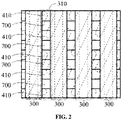
- FIG. 2 is top view of FIG. 1
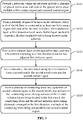
- FIG. 3 is a flowchart of a method for manufacturing a memory according to an embodiment of this disclosure
- FIG. 4 is a top view of a substrate according to an embodiment of this disclosure.
- the memory shown in FIG. 1 has two cross sections at positions C and D.
- the cross section at the position C is a central plane of trenches of the memory, that is, the cross section at the position C is perpendicular to an extending direction of bit lines 200 and passes through a word line.
- the cross section at the position D is perpendicular to the extending direction of the bit lines 200 and passes through a plurality of spaced active area 110.
- the method for manufacturing the memory in the embodiment of this disclosure includes the following steps.
- a substrate is provided.
- the substrate includes a plurality of spaced active areas, and each of the plurality of spaced active areas includes a first contact region and a second contact region.
- FIG. 4 shows the top view of the substrate 100.
- the plurality of active areas 110 are disposed in the substrate 100, and the active area 110 is shown by dotted lines in FIG. 4 , that is, the active area 110 is not exposed on a surface of the substrate 100.
- the substrate 100 further includes an insulation layer, such as a silicon oxide layer, covering the plurality of active areas 110, to isolate the plurality of active areas 110.
- the number of active areas 110 may be more than one, and the plurality of active areas 110 are arranged at intervals.
- the plurality of active areas 110 can be arranged in an array.
- a shallow trench isolation (referred to as STI for short) structure 120 is disposed between the plurality of active areas 110, and silicon oxide (SiO2) is filled in the STI structure 120.
- the plurality of active areas 110 are isolated by the STI structures 120.
- each of the plurality of active area 110 may include a first contact region 111 and a second contact region 112.
- the first contact region 111 and the second contact region 112 may be adjacent, the first contact region 111 is connected to a bit line 200, and the second contact region 112 is connected to a capacitor, to enable the bit line to read data information from the capacitor or write data information into the capacitor, so that the memory can operate normally.
- the first contact region 111 is located at a center of the active area 110, and the second contact regions 112 are located at both ends of the active area 110, that is, the second contact regions 112 are located on both sides of the first contact region 111.
- a material of the active area 110 may include silicon (Si).
- the material of the active area 110 is not limited thereto.
- the material of the active area may be germanium (Ge), silicon on insulator (referred to as SOI for short), or the like.
- a word line is further disposed in the substrate 100, and the word line may be an embedded word line.
- bit lines are formed on the substrate.
- Each of the bit lines is connected to at least one first contact region, and the bit line includes a first conductive layer, a first protection layer and a barrier layer stacked in sequence, the first conductive layer is located on the substrate.
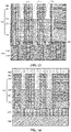
- FIG. 5 is a cross-sectional view of the position C after a first isolation layer is formed according to an embodiment of this disclosure
- FIG. 6 is a cross-sectional view of the position D after the first isolation layer is formed according to an embodiment of this disclosure.
- the cross-sectional view shown in FIG. 5 is obtained by taking a plane that is perpendicular to an extending direction of the bit line 200 and passes through a word line 140 as a cross section
- a cross-sectional view shown in FIG. 6 is obtained by taking a plane that is perpendicular to the extending direction of the bit line 200 and passes through the active area 110 as a cross section.
- the plurality of spaced bit lines 200 are formed on the substrate 100, and each of the plurality of spaced bit lines 200 is connected to at least one first contact region 111.
- the plurality of bit lines 200 are parallel to each other, and extends in a first direction.
- Each of the plurality of bit lines 200 is connected to a plurality of first contact regions 111 in a same column, that is, the plurality of first contact regions 111 in the same column are connected to one bit line 200.
- An angle is formed between an orthographic projection of the bit line 200 on the substrate 100 and an orthographic projection of the active area 110 on the substrate 100.
- the plurality of spaced bit lines 200 are disposed vertically
- the plurality of spaced active area 110 are disposed obliquely
- the plurality of spaced active areas 110 are parallel to each other.
- a third isolation layer 800 is further disposed on the substrate 100, as shown in FIG. 5 and FIG. 6 , to further isolate and protect the plurality of active areas 110.
- a material of the third isolation layer 800 is silicon nitride.
- a bit line contact region is formed in the third isolation layer 800 and the substrate 100, and the bit line contact region exposes the first contact region 111.
- the bit line 200 is formed in the bit line contact region and is in contact with the first contact region 111, to implement electrical connection between the bit line 200 and the first contact region 111.
- the bit line 200 includes a first conductive layer 210, a first protection layer 220 and a barrier layer 230 stacked in sequence, and the first conductive layer 210 is located on the substrate 100 and is electrically connected to the first contact region 111.
- a material of the first conductive layer 210 includes poly crystalline silicon, titanium nitride, and tungsten.
- the first conductive layer 210 may be of a stack structure.
- the first conductive layer 210 includes a polycrystalline silicon layer disposed on the substrate 100, a titanium nitride (TiN) layer disposed on the polycrystalline silicon layer, and a tungsten (W) layer disposed on the titanium nitride layer.
- the first protection layer 220 isolates and protects the first conductive layer 210.
- the thickness of the first protection layer 220 may be in a range of 20 nm to 40 nm, and a material of the first protection layer 220 includes silicon nitride (Si 3 N 4 ). As shown in FIG. 5 and FIG. 6 , the thickness of the first protection layer 220 is a distance in a vertical direction, that is, a height in a direction away from the substrate 100.
- the thickness of the barrier layer 230 is in a range of 20 nm to 80 nm, and a material of the barrier layer 230 includes silicon oxide.
- An etch rate selectivity of the subsequently formed conducting wire 410 and the barrier layer 230 is greater than 100, so that in the process of etching a second conductive layer 400 to form conducting wires 410, the barrier layer 230 is less etched, and further it is difficult to etch the first conductive layer 210, thereby reducing the risk of exposure of the first conductive layer 210 and improving the yield rate of the memory.
- the bit line 200 may further include a second protection layer 240, which is disposed on the barrier layer 230.
- the thickness of the second protection layer 240 is in a range of 20 nm to 80 nm, and a material of the second protection layer 240 includes silicon nitride.
- a first preset conductive layer, a first preset protection layer, a preset barrier layer, and a second preset protection layer are sequentially deposited on the substrate 100, and then parts of the first preset conductive layer, parts of the first preset protection layer, parts of the preset barrier layer, and parts of the second preset protection layer are removed, to expose the substrate 100.
- the remaining first preset conductive layer forms the first conductive layer 210
- the remaining first preset protection layer forms the first protection layer 220
- the remaining preset barrier layer forms the barrier layer 230
- the remaining second preset protection layer forms the second protection layer 240.
- the forming of the plurality of bit lines 200 is not limited and may be implemented by layer-by-layer deposition.
- the first protection layer 220, the barrier layer 230, and the second protection layer 240 are sequentially deposited on the first conductive layer 210.
- a first isolation layer is formed on the bit line, a first trench extending in a first direction is formed between two adjacent first isolation layers.
- a first isolation layer 300 is formed on the bit line 200, and the first isolation layer 300 covers the bit line 200.
- the first isolation layer 300 is formed on an upper surface and a side surface of the bit line 200, and a material of the first isolation layer 300 may be an insulation material such as silicon nitride.
- a first trench 310 is formed between two adjacent first isolation layers 300, that is, both sidewalls of the first trench 310 are the first isolation layer 300. As shown in FIG. 5 and FIG. 6 , the first trench 310 extends in a first direction and it can be understood that the extending direction of the first trench 310 is the same as the extending direction of the bit line 200.
- a plurality of oxide layers 320 may further be provided in the first isolation layer 300, as shown in FIG. 5 and FIG. 6 . Both sides of each bit line are each provided with an oxide layer 320.
- the oxide layer 320 extends in the first direction, that is, the extending direction of the oxide layer 320 is the same as the extending direction of the bit line 200.
- nitride-oxide-nitride referred to as NON for short
- NON nitride-oxide-nitride
- a bottom of the first trench is etched along the first trench to form a second trench from which the second contact region exposes.
- a bottom of the first trench 310 is etched along the first trench 310 to form a second trench 130, which is easily formed.
- a bottom of the second trench 130 is located in the substrate 100, as shown in FIG. 8 , and the second trench 130 exposes the second contact region 112.
- the first isolation layer 300 further covers the substrate 100, that is, the first isolation layer 300 is deposited on the bit line 200 and the substrate 100.
- the first isolation layer 300 and the substrate 100 are etched, and the bottom of the formed second trench 130 is located in the substrate 100.
- parts of the first isolation layer 300 away from the substrate 100 may also be removed, so that the oxide layer 320 is exposed out of a surface of the first isolation layer 300 and the oxide layer 320 is exposed out of a top surface of the first isolation layer 300.
- a plurality of conducting wires and a plurality of second isolation layers are formed in the second trench.
- the top surface of the conducting wire and the top surface of the second isolation layer are located in the first trench, the plurality of conducting wires and the plurality of second isolation layers are alternately arranged in the first direction, and each of the conducting wires is connected to one of the second contact regions.
- a plurality of conducting wires 410 and a plurality of second isolation layers 700 are disposed in each second trench 130, as shown in FIG. 1 and FIG. 2 , the conducting wires 410 and the second isolation layers 700 are alternately arranged in a first direction, and each of the plurality of conducting wires 410 is connected to one second contact region 112.
- the plurality of conducting wires 410 are separated by the first isolation layer 300 and the second isolation layer 700, to prevent the plurality of conducting wires 410 from being interconnected.
- the plurality of conducting wires 410 may be arranged in an array in the memory. For example, as shown in FIG. 1 and FIG. 2 , the plurality of conducting wires 410 may be arranged in a square array.
- a top surface of the conducting wire 410 and a top surface of the second isolation layer 700 are located in the first trench 310, and the top surface of the conducting wire 410 may not be flush with the top surface of the second isolation layer 700. As shown in FIG. 1 , for example, the top surface of the second isolation layer 700 is flush with the top surface of the first isolation layer 300, and the top surface of the conducting wire 410 is lower than the top surface of the first isolation layer 300, so that a capacitively contact pad is formed on the conducting wire 410.
- a material of the second isolation layer 700 may be the same as the material of the second isolation layer 300.
- the top surface of the conducting wire 410 may be higher than or lower than the top surface of the first conductive layer 210. That is, the top surface of the conducting wire 410 may be located on a side of the first conductive layer 210 away from the substrate 100 or on a side of the first conductive layer 210 close to the substrate 100.
- a difference between a height of the top surface of the conducting wire 410 and a height of a top surface of the first conductive layer 210 is in a range of -15 nm to 30 nm.
- the height of the top surface of the conducting wire 410 refers to a distance between the top surface of the conducting wire 410 and a top surface of the substrate 100.
- the height of the top surface of the first conductive layer 210 refers to the distance between the top surface of the first conductive layer 210 and the top surface of the substrate 100.
- the difference between the height of the top surfaces of the conducting wire 410 and the height of the top surface of the first conductive layer 210 is a value obtained by subtracting the height of the top surface of the conducting wire 410 by the height of the top surface of the first conductive layer 210.
- the difference between the height of the top surface of the conducting wire 410 and the height of the top surface of the first conductive layer 210 being negative indicates that the top surface of the conducting wire 410 is located on the side of the first conductive layer 210 close to the substrate 100
- the difference between the height of the top surface of the conducting wire 410 and the height of the top surface of the first conductive layer 210 being positive indicates that the top surface of the conducting wire 410 is located on the side of the first conductive layer 210 away from the substrate 100, as shown in FIG. 1 .
- a substrate 100 is provided first.
- the substrate 100 includes a plurality of spaced active areas 110, and each of the plurality of spaced active areas 110 includes a first contact region 111 and a second contact region 112.
- a plurality of spaced bit lines 200 are formed on the substrate 100, and each of the plurality of spaced bit lines 200 is connected to at least one first contact region 111.
- the bit line 200 includes a first conductive layer 210, a first protection layer 220 and a barrier layer 230 stacked in sequence, and the first conductive layer 210 is located on the substrate 100.
- a first isolation layer 300 is then formed on the bit line 200, a first trench 310 extending in a first direction is formed between two adjacent first isolation layers 300. A bottom of the first trench 310 is etched along the first trench 310 to form a second trench 130 from which the second contact region 112 exposes. A plurality of conducting wires 410 and a plurality of second isolation layers 700 are formed in the second trench 130.
- Top surfaces of the plurality of conducting wires 410 and top surfaces of the second isolation layers 700 are located in the first trench 310.
- the plurality of conducting wires 410 and the plurality of second isolation layers 700 are alternately arranged in the first direction, and each of the plurality of conducting wires 410 is connected to the second contact region 112.
- the conducting wire 410 is further electrically connected to a capacitively contact pad, which is electrically connected to a capacitor, so that the capacitor is electrically connected to the bit line 200 through which data information stored in the capacitor can be read or data information can be written into the capacitor.
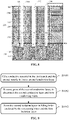
- the step that the plurality of conducting wires and the plurality of second isolation layers are formed in the second trench includes steps S1051 to S1053.
- a conductive material is filled in the first trench and the second trench, to form a second conductive layer.
- a conductive material is deposited in the first trench 310 and the second trench 130, to form a second conductive layer 400.
- the second conductive layer 400 is formed in the first trench 310 and the second trench 130 by Chemical Vapor Deposition (CVD), Physical Vapor Deposition (PVD), Atomic Layer Deposition (ALD), or the like.
- CVD Chemical Vapor Deposition
- PVD Physical Vapor Deposition
- ALD Atomic Layer Deposition
- the second conductive layer 400 is filled in the first trench 310 and the second trench 130 and covers a surface of the first isolation layer 300 away from the substrate 100.
- a conductive material may be polycrystalline silicon, that is, the material of the second conductive layer 400 may be polycrystalline silicon.
- a filling space of the first trench 310 and the second trench 130 is large, the filling difficulty is low, and the filling quality is good. Voids and/or seams caused by the non-uniform filling of the second conductive layer 400 are reduced, thereby improving the quality of forming the second conductive layer 400, and further improving the yield rate of the memory.
- the method for manufacturing the memory may further include the following steps. Parts of the second conductive layer 400 away from the substrate 100 are removed to expose parts of the first trench 310. Referring to FIG. 12 and FIG. 13 , a part of the second conductive layer 400 located on the first isolation layer 300 is removed by etching, and parts of the second conductive layer 400 located in the first trench 310 are removed by etching. As shown in FIG. 12 and FIG. 13 , partial regions of the second conductive layer 400 away from the substrate 100 are removed by etching.
- the second conductive layer 400 is etched back, to expose an upper portion of the first trench 310. As shown in FIG. 12 and FIG. 13 , after the parts of the second conductive layer 400 are removed, a sidewall of the first trench 310 is exposed, that is, parts of a side surface of the first isolation layer 300 are exposed.
- an intermediate layer 500 is formed on the second conductive layer 400, and the intermediate layer 500 is filled in the first trench 310.
- the intermediate layer 500 is deposited in the exposed part of the first trench 310 and the intermediate layer 500 is located on the second conductive layer 400. That is, a lower portion of the first trench 310 is filled up with the second conductive layer 400 and an upper portion of the first trench 310 is filled up with the intermediate layer 500.
- Such arrangement reduces a height of the second conductive layer 400, thereby reducing an etching depth of the second conductive layer 400 in subsequent etching of the second conductive layer 400.
- by-products during etching of the second conductive layer 400 are reduced, and the quality of forming the plurality of conducting wires 410 is improved.
- diffusion of the second conductive layer 400 can be reduced or even prevented, so as to improve the yield rate of the memory.
- the intermediate layer 500 may be Spin on Dielectrics (SOD), and the intermediate layer 500 is formed by spin coating a liquid insulation medium and performing a high-temperature treatment to solidify the liquid insulation medium.
- a material of the intermediate layer 500 may be an oxide such as silicon oxide.
- the intermediate layer 500 may be formed by the following processes.
- the intermediate layer 500 is formed in the first trench 310 and on the first isolation layer 300, and the first trench 310 is filled up with the intermediate layer 500.
- the intermediate layer 500 covers the first isolation layer 300 and the second conductive layer 400.
- a surface of the intermediate layer 500 away from substrate 100 is then planarized, to expose the first isolation layer 300.
- an upper surface of the intermediate layer 500 is planarized.
- planarization treatment an upper surface of the first isolation layer 300 is exposed, that is, the first isolation layer 300 is flush with the intermediate layer 500.
- the intermediate layer 500 may be planarized by Chemical Mechanical Polishing (CMP) to obtain a relatively flat intermediate layer 500.
- CMP Chemical Mechanical Polishing
- the planarization treatment is not limited.
- the planarization treatment may further be performed by a multi-layer photoresist process.
- the intermediate layer 500 is formed on the second conductive layer 400
- parts of the intermediate layer 500 is removed, to retain the intermediate layer 500 on regions of the second conductive layer 400 where the plurality of conducting wires 410 is to be formed.
- the remaining intermediate layer 500 covers the second conductive layer 400 which is subsequently used to form the plurality of conducting wires 410. It can be understood that the second conductive layer 400 below the remaining intermediate layer 500 forms the plurality of conducting wires 410.
- the second conductive layer 400 is disposed below the intermediate layer 500, and the second conductive layer 400 may be used as a stop layer of etching the intermediate layer 500, so that the second conductive layer 400 may form a self-aligned structure.
- parts of the intermediate layer 500 may be removed by a Capacitively Coupled Plasma (CCP) etching process, so that a side surface of the remaining intermediate layer 500 is relatively upright.
- CCP Capacitively Coupled Plasma
- the parts of the intermediate layer 500 are etched using an etching gas including one or more of oxygen (O 2 ), argon (Ar), methane tetrafluoride (CF4), hexafluorobutadiene (C4F6), or octafluorocyclobutane (C4F8).
- an etching gas including one or more of oxygen (O 2 ), argon (Ar), methane tetrafluoride (CF4), hexafluorobutadiene (C4F6), or octafluorocyclobutane (C4F8).
- the third trench 510 is a region enclosed by dotted lines as shown in FIG. 18 .
- the third trench 510 exposes the barrier layer 230.
- the second direction may be perpendicular to the first direction, that is, the second direction is perpendicular to the extending direction of the spaced bit line 200.
- parts of the sidewalls of the third trench 510 are the first isolation layer 300, parts of the sidewalls of the third trench 510 are the intermediate layer 500, and the intermediate layer 500 and the first isolation layer 300 are alternately arranged in the second direction.
- Parts of the bottom of the third trench 510 are the barrier layer 230, parts of the bottom of the third trench 510 are the intermediate layer 500, and the barrier layer 230 and the intermediate layer 500 are alternately arranged in the second direction.
- the barrier layer 230 located at the bottom of the third trench is then removed to expose the second conductive layer 400.
- parts of the second conductive layer 400 are exposed, and parts of the second conductive layer 400 are located under the intermediate layer 500 and are not exposed.
- the bit lines 200 may also be etched.
- parts of the second protection layer 240 in the bit line 200 are also removed.
- step S1052 parts of the second conductive layer are removed, to disconnect the second conductive layer and form a plurality of conducting wires.
- the second conductive layer 400 is etched to remove parts of the second conductive layer 400, and remaining second conductive layer 400 and the first isolation layer 300 enclose a plurality of filling holes 600, which may be formed by one-time etching.
- the plurality of filling holes 600 partitions the second conductive layer 400 into a plurality of conducting wires 410, that is, the remaining second conductive layer 400 forms the plurality of spaced conducting wires 410, each of which is electrically connected to the second contact region 112.
- one active area 110 may be connected to two conducting wires 410, or one active area 110 may be connected to one conducting wire 410.
- the intermediate layer 500 is disposed on the second conductive layer 400. Parts of the intermediate layer 500 away from the substrate 100 and parts of the first isolation layer 300 are etched to form a third trench. The intermediate layer 500 located at a bottom of the third trench are then etched, to expose parts of the second conductive layer 400. the exposed second conductive layer 400 is continuously etched, until the second contact region 112 of the substrate 100 is exposed.
- intermediate layer 500 When removing the parts of the second conductive layer 400, remaining intermediate layer 500 may be used as a mask of the second conductive layer 400, and parts of the second conductive layer 400 that are not covered by the intermediate layer 500 are etched without additionally disposing a mask, thus reducing the manufacturing steps.
- the second conductive layer 400 is etched using an etching gas including one or more of chlorine (Cl 2 ), hydrobromic acid (HBr), helium (He), argon (Ar), methane tetrafluoride (CF4), nitrogen trifluoride (NF 3 ), or trifluoromethane (CHF3).
- An etching stop layer for etching the second conductive layer 400 may be the third isolation layer 800.
- an etch rate selectivity of the second conductive layer 400 to the barrier layer 230 is relatively large. Therefore when etching the second conductive layer 400, the barrier layer 230 is not easy to be etched after the second protection layer 240 is removed by etching, so that at least parts of the barrier layer 230 are retained, to protect the first conductive layer 210 under the barrier layer 230 and prevent the first conductive layer 210 from being exposed.
- the second conductive layer 400 is made of polycrystalline silicon and the barrier layer 230 is made of silicon oxide.
- the second isolation layer is formed in a filling hole that is enclosed by the conducting wire and the first isolation layer.
- the second isolation layer 700 may be formed by a deposition process, and a material of the second isolation layer 700 may be an insulation material, such as silicon nitride, to electrically isolate the plurality of conducting wires 410 together with the first isolation layer 300. It can be understood that the plurality of conducting wires 410 are separated by the first isolation layer 300 and the second isolation layers 700, to prevent two adjacent conducting wires 410 from being conducted, thereby ensuring normal operations of the memory.
- the step of forming the second isolation layer 700 in the filling hole 600 that are enclosed by the conducting wire 410 and the first isolation layer 300 includes: depositing the second isolation layer 700 in the filling hole 600 and the third trench.
- the remaining intermediate layer 500 is removed, so as to expose the conducting wires 410.
- a top surface of the second isolation layer 700 is flush with the top surface of the first isolation layer 300 and higher than the top surface of the conducting wire 410. That is, the conducting wire 410 is recessed toward the substrate 100 with respect to the first isolation layer 300 and the second isolation layer 700.
- the second isolation layer 700 After the second isolation layer 700 is formed, it not required to etch in a regions enclosed by the first isolation layer 300 and the second isolation layer 700, to reduce the risk of etching and damaging the first isolation layer 300, and reduce the risk of exposure of the first conductive layer 210, thereby improving the yield rate of the memory.
- a capacitively contact pad 900 is formed on each of the plurality of conducting wires 410. As shown in FIG. 26 , a plurality of capacitively contact pads 900 are provided, the plurality of capacitively contact pads 900 are in a one-to-one correspondence to the plurality of conducting wires 410, and the capacitively contact pad 900 is electrically connected to the conducting wire 410 corresponding to the capacitively contact pad 900.
- the embodiment of this disclosure further provides a memory, including: a substrate 100, a plurality of spaced bit lines 200 formed on the substrate 100, and an isolation layer covering the plurality of bit lines 200.
- the substrate 100 includes a plurality of spaced active areas 110.
- the plurality of active areas 110 are arranged in an array.
- STI structures 120 are provided between the plurality of active areas 110, and silicon oxide is provided in the STI structures 120 to isolate the plurality of active areas 110.
- a material of the active area 110 may include silicon.
- each of the plurality of active area 110 includes a first contact region 111 and a second contact region 112.
- the first contact region 111 is adjacent to the second contact regions 112
- the first contact region 111 is located at a center of the active area 110
- the second contact regions 112 are located at both ends of the active area 110, that is, the second contact regions 112 are located on both sides of the first contact region 111.
- the first contact region 111 is connected to the bit line 200
- the second contact region 112 is connected to a capacitor.
- Each of the plurality of bit lines 200 passes through first contact regions 111 of multiple active areas 110. As shown in FIG. 2 , each of the plurality of bit line 200 passes through a plurality of active areas 110 in the same column and is located on the first contact regions 111 of the plurality of active areas 110.
- Each of the plurality of bit lines 200 includes a first conductive layer 210, a first protection layer 220 and a barrier layer 230 stacked in sequence.
- the first conductive layer 210 is located on the substrate 100. It can be understood that the first protection layer 220 is disposed on the first conductive layer 210 and the barrier layer 230 is disposed on the first protection layer 220.
- the first conductive layer 210 is electrically connected to the plurality of spaced active area 110.
- the first conductive layer 210 may be of a stack structure.
- the first conductive layer 210 includes a polycrystalline silicon layer disposed on the substrate 100, a silicon nitride layer disposed on the polycrystalline silicon layer, and a tungsten layer disposed on the silicon nitride layer. That is, the tungsten layer is disposed at an end away from the substrate 100.
- the first protection layer 220 isolates and protects the first conductive layer 210.
- the thickness of the first protection layer 220 may be in a range of 20 nm to 40 nm, and a material of the first protection layer 220 may be an insulation material.
- a material of the first protection layer 220 is silicon nitride.
- the thickness of the first protection layer 220 refers to a height of the first protection layer 220 in a direction away from the substrate 100.
- the thickness of the barrier layer 230 is in a range of 20 nm to 80 nm.
- a material of the barrier layer 230 is correlated to the material of the conducting wires 410 to be formed subsequently.
- An etch rate selectivity of the conducting wire 410 to the barrier layer 230 is great, so that in the process of etching the second conductive layer 400 to form the conducting wires 410, the barrier layer 230 is less etched, and further it is difficult to etch the first conductive layer 210, to reduce the risk of exposing the first conductive layer 210 and improve the yield rate of the memory.
- an etch rate selectivity of the conducting wire 410 to the barrier layer 230 is greater than 100, the conducting wires 410 are made of polycrystalline silicon, and the barrier layer 230 is made of silicon oxide.
- the bit line 200 may further include a second protection layer 240, and the second protection layer 240 is disposed on the barrier layer 230.
- the thickness of the second protection layer 240 is in a range of 20 nm to 80 nm, and a material of the second protection layer 240 may be the same as that of the first isolation layer 300.
- the material of the second protection layer 240 includes silicon nitride.
- the isolation layer covers the plurality of spaced bit lines 200 and the substrate 100.
- the isolation layer is usually an insulation material, to further protect and isolate the plurality of spaced bit lines 200.
- the isolation layer is provided with wire holes running through the isolation layer to accommodate the plurality of conducting wires 410. Top surfaces of the plurality of conducting wires 410 may be lower than a top surface of the isolation layer, that is, the plurality of conducting wires 410 does not fill up the wire holes.
- the plurality of conducting wires 410 are recessed with respect to the isolation layer, to facilitate forming of other spaced structures, such as capacitively contact pads, on the plurality of conducting wires 410.
- a plurality of oxide layers 320 such as silicon oxide, may further be provided in the isolation layer. Both sides of each of the plurality of bit lines 200 are each provided with an oxide layer 320.
- the oxide layer 320 extends in the first direction, that is, the extending direction of the oxide layer 320 is the same as the extending direction of the bit lines 200.
- a difference between a height of the top surface of the conducting wire 410 and a height of a top surface of the first conductive layer 210 is in a range of -15 nm to 30 nm.
- the height of the top surface of the conducting wire 410 refers to a distance between the top surface of the conducting wire 410 and a top surface of the substrate 100.
- the height of the top surface of the first conductive layer 210 refers to a distance between the top surface of the first conductive layer 210 and the top surface of the substrate 100.
- the difference between the height of the top surface of the conducting wire 410 and the height of the top surface of the first conductive layer 210 is a value obtained by subtracting the height of the top surface of the conducting wire 410 by the height of the top surface of the first conductive layer 210.
- Each of the plurality of conducting wires 410 may extend into the substrate 100 and be in contact with a part of the active area 110, for example, in contact with the second contact region 112 in the active area 110. There is an isolation layer between the wire hole and the bit line 200, so that the conducting wire 410 is not directly conducted to the bit line 200. It can be understood that the top surface of the substrate 100 is provided with a contact recess opposite to and communicated with the wire hole, and the conducting wire 410 is filled in the contact recesse and the wire hole.
- a memory includes a substrate 100, a plurality of spaced bit lines 200 formed on the substrate 100, an isolation layer covering the plurality of spaced bit lines 200 and the substrate 100, and a plurality of conducting wires 410 disposed in the isolation layer and extending to the substrate 100.
- the substrate 100 includes a plurality of spaced active areas 110. Each of the plurality of spaced active areas 110 includes a first contact region 111 and a second contact region 112. Each of the plurality of bit lines 200 is connected to at least one first contact region.
- the bit line 200 includes a first conductive layer 210, a first protection layer 220 and a barrier layer 230 stacked in sequence, the first conductive layer 210 is located on the substrate 100.
- the isolation layer is provided with wire holes running through the isolation layer.
- the plurality of conducting wires 410 extending into the substrate 100 and electrically connected to the second contact regions 112 are provided in the wire holes.
- Each of the plurality of conducting wires 410 is further electrically connected to a capacitively contact pad, and the capacitively contact pad is electrically connected to a capacitor, so that the capacitor is electrically connected to the plurality of bit lines 200.
Landscapes
- Engineering & Computer Science (AREA)
- Manufacturing & Machinery (AREA)
- Internal Circuitry In Semiconductor Integrated Circuit Devices (AREA)
- Semiconductor Memories (AREA)
Abstract
Description
- This application claims priority to
Chinese Patent Application No.: 202110343740.5, filed on March 30, 2021 - This disclosure relates to the technical field of storage devices, and in particular, to a method for manufacturing a memory and a memory.
- A Dynamic Random Access Memory (DRAM) is a semiconductor memory which randomly writes and reads data at a high speed, and is widely applied in various electronic devices due to its high storage density and fast reading and writing speeds.
- In the related art, a DRAM generally includes a substrate. The substrate includes an active area, and the substrate is provided with spaced bit lines and an isolation layer covering the bit lines. The bit lines are electrically connected to the active area, a wire hole extending to the active area is formed in the isolation layer, a conducting wire is filled in the wire hole, and the conducting wire is electrically connected to the active area. To increase the contact area between the conducting wire and the active area, a contact recess is usually formed on a surface of the substrate in the wire hole. However, in a process of manufacturing a memory, a first conductive layer of the bit line is subject to be exposed or even be damaged, so that the bit line is connected to another structure, which results in a relatively low yield rate of the memory.
- The embodiment of this disclosure provides a method for manufacturing a memory, which includes: providing a substrate, where the substrate includes a plurality of spaced active areas and each of the plurality of spaced active area includes a first contact region and a second contact region; forming a plurality of spaced bit lines on the substrate, where each of the plurality of spaced bit lines is connected to at least one first contact region, and each of the plurality of spaced bit lines includes a first conductive layer, a first protection layer, and a barrier layer stacked in sequence, the first conductive layer being located on the substrate; forming a first isolation layer on each of the plurality of spaced bit lines, and forming a first trench extending in a first direction between two adjacent first isolation layers of the plurality of spaced bit lines; etching a bottom of the first trench along the first trench to form a second trench, the second trench exposing the second contact region; and forming a plurality of conducting wires and a plurality of second isolation layers in the second trench, top surfaces of the plurality of conducting wires and top surfaces of the plurality of second isolation layers being located in the first trench, the plurality of conducting wires and the plurality of second isolation layers being alternately arranged in the first direction, and each of the plurality of conducting wires being connected to the second contact region.
- The method for manufacturing the memory provided in the embodiment of this disclosure has the following advantages.
- In the method for manufacturing a memory provided in the embodiment of this disclosure, a substrate is provided. The substrate includes a plurality of spaced active areas, and each of the plurality of spaced active area includes a first contact region and a second contact region. A plurality of spaced bit lines are formed on the substrate. Each of the plurality of spaced bit lines is connected to at least one first contact region, and each of the plurality of spaced bit lines includes a first conductive layer, a first protection layer, and a barrier layer stacked in sequence, and the first conductive layer is located on the substrate. The barrier layer is arranged on the first conductive layer, and thus is not easy to be removed, to reduce a risk of exposing the first conductive layer, and avoid electrical connection between the bit line and another structure, thereby improving the yield rate of the memory. A first isolation layer is formed on each of the plurality of spaced bit lines, a first trench extending in a first direction is formed between two adjacent first isolation layers. A bottom of the first trench is etched along the first trench to form a second trench, and the second trench exposes the second contact region. A plurality of conducting wires and a plurality of second isolation layers are formed in the second trench. Top surfaces of the plurality of conducting wires and top surfaces of the plurality of second isolation layers are located in the first trench, the plurality of conducting wires and the plurality of second isolation layers are alternately arranged in the first direction, and each of the plurality of conducting wires is connected to the second contact region. The conducting wires are electrically connected with a capacitively contact pad, and the capacitively contact pad is electrically connected with a capacitor. Therefore, the capacitor is electrically conencted with the bit lines, and data information stored in the capacitor can be read through the bit lines, or data information can be written into the capacitor through the bit lines.
- The embodiment further provides a memory, including: a substrate, where the substrate includes a plurality of spaced active areas, and each of the plurality of spaced active area includes a first contact region and a second contact region; a plurality of spaced bit lines, where each of the plurality of spaced bit lines is connected to at least one first contact region, and each of the plurality of spaced bit lines includes a first conductive layer, a first protection layer and a barrier layer stacked in sequence, the first conductive layer being located on the substrate; and isolation layers covering the plurality of spaced bit lines and the substrate, where each of the isolation layers is provided with wire holes running through the isolation layers, and conducting wires extending to the substrate and electrically connected to the second contact region are provided through the wire holes.
- The memory provided in the embodiment of this disclosure has the following advantages.
- The memory provided in the embodiment of this disclosure includes a substract, and a plurality of spaced bit lines arranged on the substract, and isolation layers covering the plurality of spaced bit lines and the substrate, and conducting wires arranged on the isolation layers and extending to the substrate. The substract includes a plurality of spaced active areas, and each of the plurality of spaced active area includes a first contact region and a second contact region. Each of the plurality of spaced bit lines is connected to at least one first contact region. Each of the plurality of spaced bit lines includes a first conductive layer, a first protection layer and a barrier layer stacked in sequence. The first conductive layer is located on the substrate, and the barrier layer is provided on the first conductive layer. Therefore, the barrier layer is not easy to be removed, to reduce a risk of exposing the first conductive layer, and avoid electrical connection between the bit line and another structure, thereby improving the yield rate of the memory. The isolation layers are provided with wire holes running through the isolation layers, and conducting wires extending to the substrate and electrically connected to the second contact region are provided through the wire holes. The conducting wires are electrically connected with a capacitively contact pad, and the capacitively contact pad is electrically connected with a capacitor. Therefore, the capacitor is electrically conencted with the bit lines, and data information stored in the capacitor can be read through the bit lines, or data information can be written into the capacitor through the bit lines.
-
-
FIG. 1 is a schematic structural diagram of a memory according to an embodiment of this disclosure. -
FIG. 2 is a top view of of a memory shown inFIG. 1 . -
FIG. 3 is a flowchart of a method for manufacturing a memory according to an embodiment of this disclosure. -
FIG. 4 is a top view of a substrate according to an embodiment of this disclosure. -
FIG. 5 is a cross-sectional view of a position C after a first isolation layer is formed according to an embodiment of this disclosure. -
FIG. 6 is a cross-sectional view of a position D after a first isolation layer is formed according to an embodiment of this disclosure. -
FIG. 7 is a cross-sectional view of a position C after second trenches are formed according to an embodiment of this disclosure. -
FIG. 8 is a cross-sectional view of a position D after the second trenches are formed according to an embodiment of this disclosure. -
FIG. 9 is a flowchart of forming a plurality of conducting wires and a plurality of second isolation layers in a second trench according to an embodiment of this disclosure. -
FIG. 10 is a cross-sectional view of a position C after a second conductive layer is formed according to an embodiment of this disclosure. -
FIG. 11 is a cross-sectional view of a position D after a second conductive layer is formed according to an embodiment of this disclosure. -
FIG. 12 is a cross-sectional view of a position C after parts of a second conductive layer are removed according to an embodiment of this disclosure. -
FIG. 13 is a cross-sectional view of a position D after parts of a second conductive layer are removed according to an embodiment of this disclosure. -
FIG. 14 is a cross-sectional view of a position C after an intermediate layer is formed according to an embodiment of this disclosure. -
FIG. 15 is a cross-sectional view of a position D after an intermediate layer is formed according to an embodiment of this disclosure. -
FIG. 16 is a cross-sectional view of a position C after an intermediate layer is planarized according to an embodiment of this disclosure. -
FIG. 17 is a cross-sectional view of a position D after an intermediate layer is planarized according to an embodiment of this disclosure. -
FIG. 18 is a cross-sectional view of a position C after parts of an intermediate layer are removed according to an embodiment of this disclosure. -
FIG. 19 is a cross-sectional view of a position D after parts of an intermediate layer are removed according to an embodiment of this disclosure. -
FIG. 20 is a cross-sectional view of a position C after conducting wires are formed according to an embodiment of this disclosure. -
FIG. 21 is a cross-sectional view of a position D after conducting wires are formed according to an embodiment of this disclosure. -
FIG. 22 is a cross-sectional view of a position C after a second isolation layer is formed according to an embodiment of this disclosure. -
FIG. 23 is a cross-sectional view of a position D after a second isolation layer is formed according to an embodiment of this disclosure. -
FIG. 24 is a cross-sectional view of a position C after remaining intermediate layer is removed according to an embodiment of this disclosure. -
FIG. 25 is a cross-sectional view of a position D after remaining intermediate layer is removed according to an embodiment of this disclosure. -
FIG. 26 is a cross-sectional view of a position D after capacitively contact pads are formed according to an embodiment of this disclosure. - In related technology, when manufacturing a memory, a plurality of bit lines and a first isolation layer covering the plurality of bit lines are generally formed on a substrate. The substrate includes a plurality of spaced active areas, each of the plurality of spaced active areas includes a first contact region and a second contact region, each of the plurality of spaced bit lines is connected to at least one first contact region, and a first trench is formed between first isolation layers of two adjacent bit lines. An intermediate layer is deposited in the first trench, and the first trench is filled up with the intermediate layer. The intermediate layer is etched to form first through-holes, and the remaining intermediate layer forms a plurality of spaced columnar structures, and each of the plurality of spaced columnar structures corresponds to one second contact region. A second isolation layer is deposited in the first through-holes, the remaining intermediate layer is removed to form second through-holes. The substrate is etched along the second through-holes to form contact recesses. The contact recesses expose the second contact regions. A conductive material is filled in the contact recesses and the second through-holes to form conducting wires.
- In the above-mentioned manufacturing process, when etching the substrate along the second through-hole, the first isolation layer outside the plurality of spaced bit lines is subject to be etched through. As a result, conducting wires are conducted to the plurality of spaced bit lines, thereby causing the failure of the memory and a low yield rate of the memory. In addition, the intermediate layer is removed through etching twice, which is a complicated removal process, and the residual intermediate layer may further cause the low yield rate of the memory.
- To this end, the manufacturing process of the memory may be changed. First, a bottom of the first trench is etched along the first trench formed by the first isolation layer to form a second trench, a second conductive layer is formed in the first trench and the second trench, and then the second conductive layer is etched to disconnect the second conductive layer and form the conducting wires. However, in the above-mentioned process, parts of the first isolation layer may also be removed when etching the second conductive layer, so that the plurality of spaced bit lines in the first isolation layer is subject to be exposed or even damaged, resulting in relatively low yield rate of the memory.
- To prevent from exposing or even damaging a first conductive layer of a bit line in a process of manufacturing a memory, the embodiments of this disclosure provides a method for manufacturing a memory, which includes operations as follows. A substrate is provided. The substrate includes a plurality of spaced active areas, and each of the plurality of spaced active areas includes a first contact region and a second contact region. A plurality of spaced bit lines are formed on the substrate. Each of the plurality of spaced bit lines is connected to at least one first contact region, and each of the plurality of spaced bit lines includes a first conductive layer, a first protection layer and a barrier layer stacked in sequence, and the first conductive layer is located on the substrate. A first isolation layer is formed on each of the plurality of spaced bit lines, a first trench extending in a first direction is formed between two adjacent first isolation layers of the plurality of spaced bit lines. A bottom of the first trench is etched along the first trench to form a second trench from which the second contact region exposes. A plurality of conducting wires and a plurality of second isolation layers are formed in the second trench, and top surfaces of the plurality of conducting wires and top surfaces of the plurality of second isolation layers are located in the first trench. The plurality of conducting wires and the plurality of second isolation layers are alternately arranged in the first direction, and each of the plurality of conducting wires is connected to one second contact region. By disposing the barrier layer above the first conductive layer, the barrier layer is difficult to be removed, to reduce the risk of exposing the first conductive layer and avoid an electrical connection between a bit line and another structure, thereby improving the yield rate of the memory.
- To make the above objectives, features, and advantages of the embodiments of this application more apparent and easy to understand, the technical solutions in the embodiments of this disclosure are clearly and completely described with reference to accompanying drawings in the embodiments of this disclosure. Apparently, the described embodiments are merely some rather than all of the embodiments of this disclosure. Other embodiments derived based on the embodiments of this disclosure by a person of ordinary skill in the art without creative efforts shall fall within the protection scope of this disclosure.
- Referring to
FIG. 1 to FIG. 4 ,FIG. 1 is a schematic structural diagram of a memory according to an embodiment of this disclosure,FIG. 2 is top view ofFIG. 1 ,FIG. 3 is a flowchart of a method for manufacturing a memory according to an embodiment of this disclosure, andFIG. 4 is a top view of a substrate according to an embodiment of this disclosure. - The memory shown in
FIG. 1 has two cross sections at positions C and D. The cross section at the position C is a central plane of trenches of the memory, that is, the cross section at the position C is perpendicular to an extending direction ofbit lines 200 and passes through a word line. The cross section at the position D is perpendicular to the extending direction of thebit lines 200 and passes through a plurality of spacedactive area 110. Referring toFIG. 3 , the method for manufacturing the memory in the embodiment of this disclosure includes the following steps. - At step S101, a substrate is provided. The substrate includes a plurality of spaced active areas, and each of the plurality of spaced active areas includes a first contact region and a second contact region.
- Referring to
FIG. 4, FIG. 4 shows the top view of thesubstrate 100. As shown inFIG. 4 , the plurality ofactive areas 110 are disposed in thesubstrate 100, and theactive area 110 is shown by dotted lines inFIG. 4 , that is, theactive area 110 is not exposed on a surface of thesubstrate 100. For example, thesubstrate 100 further includes an insulation layer, such as a silicon oxide layer, covering the plurality ofactive areas 110, to isolate the plurality ofactive areas 110. - The number of
active areas 110 may be more than one, and the plurality ofactive areas 110 are arranged at intervals. For example, the plurality ofactive areas 110 can be arranged in an array. In a possible example, a shallow trench isolation (referred to as STI for short)structure 120 is disposed between the plurality ofactive areas 110, and silicon oxide (SiO2) is filled in theSTI structure 120. The plurality ofactive areas 110 are isolated by theSTI structures 120. - Still referring to
FIG. 4 , each of the plurality ofactive area 110 may include afirst contact region 111 and asecond contact region 112. For example, thefirst contact region 111 and thesecond contact region 112 may be adjacent, thefirst contact region 111 is connected to abit line 200, and thesecond contact region 112 is connected to a capacitor, to enable the bit line to read data information from the capacitor or write data information into the capacitor, so that the memory can operate normally. - In a possible example, the
first contact region 111 is located at a center of theactive area 110, and thesecond contact regions 112 are located at both ends of theactive area 110, that is, thesecond contact regions 112 are located on both sides of thefirst contact region 111. A material of theactive area 110 may include silicon (Si). Certainly, the material of theactive area 110 is not limited thereto. For example, the material of the active area may be germanium (Ge), silicon on insulator (referred to as SOI for short), or the like. It should be noted that, a word line is further disposed in thesubstrate 100, and the word line may be an embedded word line. - Referring to step S102, a plurality of spaced bit lines are formed on the substrate. Each of the bit lines is connected to at least one first contact region, and the bit line includes a first conductive layer, a first protection layer and a barrier layer stacked in sequence, the first conductive layer is located on the substrate.
- Referring to
FIG. 5 andFIG. 6 ,FIG. 5 is a cross-sectional view of the position C after a first isolation layer is formed according to an embodiment of this disclosure, andFIG. 6 is a cross-sectional view of the position D after the first isolation layer is formed according to an embodiment of this disclosure. It can be understood that after the first isolation layer is formed, the cross-sectional view shown inFIG. 5 is obtained by taking a plane that is perpendicular to an extending direction of thebit line 200 and passes through aword line 140 as a cross section, and a cross-sectional view shown inFIG. 6 is obtained by taking a plane that is perpendicular to the extending direction of thebit line 200 and passes through theactive area 110 as a cross section. For meanings of the cross-sectional views at positions C and D in the following embodiments, reference may be made to the above content and details are not described again. - As shown in
FIG. 5 andFIG. 6 , the plurality of spacedbit lines 200 are formed on thesubstrate 100, and each of the plurality of spacedbit lines 200 is connected to at least onefirst contact region 111. The plurality ofbit lines 200 are parallel to each other, and extends in a first direction. Each of the plurality ofbit lines 200 is connected to a plurality offirst contact regions 111 in a same column, that is, the plurality offirst contact regions 111 in the same column are connected to onebit line 200. - An angle is formed between an orthographic projection of the
bit line 200 on thesubstrate 100 and an orthographic projection of theactive area 110 on thesubstrate 100. In an orientation shown inFIG. 2 , the plurality of spacedbit lines 200 are disposed vertically, the plurality of spacedactive area 110 are disposed obliquely, and the plurality of spacedactive areas 110 are parallel to each other. - It should be noted that, a
third isolation layer 800 is further disposed on thesubstrate 100, as shown inFIG. 5 andFIG. 6 , to further isolate and protect the plurality ofactive areas 110. For example, a material of thethird isolation layer 800 is silicon nitride. A bit line contact region is formed in thethird isolation layer 800 and thesubstrate 100, and the bit line contact region exposes thefirst contact region 111. Thebit line 200 is formed in the bit line contact region and is in contact with thefirst contact region 111, to implement electrical connection between thebit line 200 and thefirst contact region 111. - Continuously referring to
FIG. 5 andFIG. 6 , thebit line 200 includes a firstconductive layer 210, afirst protection layer 220 and abarrier layer 230 stacked in sequence, and the firstconductive layer 210 is located on thesubstrate 100 and is electrically connected to thefirst contact region 111. - A material of the first
conductive layer 210 includes poly crystalline silicon, titanium nitride, and tungsten. For example, the firstconductive layer 210 may be of a stack structure. For example, as shown inFIG. 5 andFIG. 6 , the firstconductive layer 210 includes a polycrystalline silicon layer disposed on thesubstrate 100, a titanium nitride (TiN) layer disposed on the polycrystalline silicon layer, and a tungsten (W) layer disposed on the titanium nitride layer. - Still referring to
FIG. 5 andFIG. 6 , thefirst protection layer 220 isolates and protects the firstconductive layer 210. The thickness of thefirst protection layer 220 may be in a range of 20 nm to 40 nm, and a material of thefirst protection layer 220 includes silicon nitride (Si3N4). As shown inFIG. 5 andFIG. 6 , the thickness of thefirst protection layer 220 is a distance in a vertical direction, that is, a height in a direction away from thesubstrate 100. - The thickness of the
barrier layer 230 is in a range of 20 nm to 80 nm, and a material of thebarrier layer 230 includes silicon oxide. An etch rate selectivity of the subsequently formed conductingwire 410 and thebarrier layer 230 is greater than 100, so that in the process of etching a secondconductive layer 400 to form conductingwires 410, thebarrier layer 230 is less etched, and further it is difficult to etch the firstconductive layer 210, thereby reducing the risk of exposure of the firstconductive layer 210 and improving the yield rate of the memory. - Still referring to
FIG. 5 andFIG. 6 , thebit line 200 may further include asecond protection layer 240, which is disposed on thebarrier layer 230. The thickness of thesecond protection layer 240 is in a range of 20 nm to 80 nm, and a material of thesecond protection layer 240 includes silicon nitride. - In a possible example, a first preset conductive layer, a first preset protection layer, a preset barrier layer, and a second preset protection layer are sequentially deposited on the
substrate 100, and then parts of the first preset conductive layer, parts of the first preset protection layer, parts of the preset barrier layer, and parts of the second preset protection layer are removed, to expose thesubstrate 100. - It can be understood that the remaining first preset conductive layer forms the first
conductive layer 210, the remaining first preset protection layer forms thefirst protection layer 220, the remaining preset barrier layer forms thebarrier layer 230, and the remaining second preset protection layer forms thesecond protection layer 240. Certainly, the forming of the plurality ofbit lines 200 is not limited and may be implemented by layer-by-layer deposition. For example, thefirst protection layer 220, thebarrier layer 230, and thesecond protection layer 240 are sequentially deposited on the firstconductive layer 210. - At step S103, a first isolation layer is formed on the bit line, a first trench extending in a first direction is formed between two adjacent first isolation layers.
- Still referring to
FIG. 5 andFIG. 6 , after thebit line 200 is formed, afirst isolation layer 300 is formed on thebit line 200, and thefirst isolation layer 300 covers thebit line 200. As shown inFIG. 5 andFIG. 6 , thefirst isolation layer 300 is formed on an upper surface and a side surface of thebit line 200, and a material of thefirst isolation layer 300 may be an insulation material such as silicon nitride. - A
first trench 310 is formed between two adjacent first isolation layers 300, that is, both sidewalls of thefirst trench 310 are thefirst isolation layer 300. As shown inFIG. 5 andFIG. 6 , thefirst trench 310 extends in a first direction and it can be understood that the extending direction of thefirst trench 310 is the same as the extending direction of thebit line 200. - A plurality of
oxide layers 320, such as silicon oxide, may further be provided in thefirst isolation layer 300, as shown inFIG. 5 andFIG. 6 . Both sides of each bit line are each provided with anoxide layer 320. Theoxide layer 320 extends in the first direction, that is, the extending direction of theoxide layer 320 is the same as the extending direction of thebit line 200. It can be understood that nitride-oxide-nitride (referred to as NON for short) are sequentially formed outside of thebit line 200 along a direction from thebit line 200 to thefirst trench 310. - At step S104, a bottom of the first trench is etched along the first trench to form a second trench from which the second contact region exposes.
- Referring to
FIG. 7 andFIG. 8 , a bottom of thefirst trench 310 is etched along thefirst trench 310 to form asecond trench 130, which is easily formed. A bottom of thesecond trench 130 is located in thesubstrate 100, as shown inFIG. 8 , and thesecond trench 130 exposes thesecond contact region 112. - In a possible example, the
first isolation layer 300 further covers thesubstrate 100, that is, thefirst isolation layer 300 is deposited on thebit line 200 and thesubstrate 100. When etching the bottom of thefirst trench 310 along thefirst trench 310, thefirst isolation layer 300 and thesubstrate 100 are etched, and the bottom of the formedsecond trench 130 is located in thesubstrate 100. - It can be understood that, in some possible examples, when etching the
first isolation layer 300 and thesubstrate 100 along thefirst trench 310, parts of thefirst isolation layer 300 away from thesubstrate 100 may also be removed, so that theoxide layer 320 is exposed out of a surface of thefirst isolation layer 300 and theoxide layer 320 is exposed out of a top surface of thefirst isolation layer 300. - At step S105, a plurality of conducting wires and a plurality of second isolation layers are formed in the second trench. The top surface of the conducting wire and the top surface of the second isolation layer are located in the first trench, the plurality of conducting wires and the plurality of second isolation layers are alternately arranged in the first direction, and each of the conducting wires is connected to one of the second contact regions.
- A plurality of conducting
wires 410 and a plurality of second isolation layers 700 are disposed in eachsecond trench 130, as shown inFIG. 1 andFIG. 2 , the conductingwires 410 and the second isolation layers 700 are alternately arranged in a first direction, and each of the plurality of conductingwires 410 is connected to onesecond contact region 112. The plurality of conductingwires 410 are separated by thefirst isolation layer 300 and thesecond isolation layer 700, to prevent the plurality of conductingwires 410 from being interconnected. The plurality of conductingwires 410 may be arranged in an array in the memory. For example, as shown inFIG. 1 andFIG. 2 , the plurality of conductingwires 410 may be arranged in a square array. - A top surface of the
conducting wire 410 and a top surface of thesecond isolation layer 700 are located in thefirst trench 310, and the top surface of theconducting wire 410 may not be flush with the top surface of thesecond isolation layer 700. As shown inFIG. 1 , for example, the top surface of thesecond isolation layer 700 is flush with the top surface of thefirst isolation layer 300, and the top surface of theconducting wire 410 is lower than the top surface of thefirst isolation layer 300, so that a capacitively contact pad is formed on theconducting wire 410. A material of thesecond isolation layer 700 may be the same as the material of thesecond isolation layer 300. - The top surface of the
conducting wire 410 may be higher than or lower than the top surface of the firstconductive layer 210. That is, the top surface of theconducting wire 410 may be located on a side of the firstconductive layer 210 away from thesubstrate 100 or on a side of the firstconductive layer 210 close to thesubstrate 100. - In a possible example, a difference between a height of the top surface of the
conducting wire 410 and a height of a top surface of the firstconductive layer 210 is in a range of -15 nm to 30 nm. The height of the top surface of theconducting wire 410 refers to a distance between the top surface of theconducting wire 410 and a top surface of thesubstrate 100. The height of the top surface of the firstconductive layer 210 refers to the distance between the top surface of the firstconductive layer 210 and the top surface of thesubstrate 100. The difference between the height of the top surfaces of theconducting wire 410 and the height of the top surface of the firstconductive layer 210 is a value obtained by subtracting the height of the top surface of theconducting wire 410 by the height of the top surface of the firstconductive layer 210. - It can be understood that the difference between the height of the top surface of the
conducting wire 410 and the height of the top surface of the firstconductive layer 210 being negative indicates that the top surface of theconducting wire 410 is located on the side of the firstconductive layer 210 close to thesubstrate 100, and the difference between the height of the top surface of theconducting wire 410 and the height of the top surface of the firstconductive layer 210 being positive indicates that the top surface of theconducting wire 410 is located on the side of the firstconductive layer 210 away from thesubstrate 100, as shown inFIG. 1 . - In the method for manufacturing the memory according to the embodiment of this disclosure, a
substrate 100 is provided first. Thesubstrate 100 includes a plurality of spacedactive areas 110, and each of the plurality of spacedactive areas 110 includes afirst contact region 111 and asecond contact region 112. A plurality of spacedbit lines 200 are formed on thesubstrate 100, and each of the plurality of spacedbit lines 200 is connected to at least onefirst contact region 111. Thebit line 200 includes a firstconductive layer 210, afirst protection layer 220 and abarrier layer 230 stacked in sequence, and the firstconductive layer 210 is located on thesubstrate 100. By disposing thebarrier layer 230 on the firstconductive layer 210, thebarrier layer 230 is not easy to be removed, and thus thebarrier layer 230 can reduce the risk of exposure of the firstconductive layer 210, to avoid an electrical connection between thebit line 200 and another structure, thereby improving the yield rate of the memory. Afirst isolation layer 300 is then formed on thebit line 200, afirst trench 310 extending in a first direction is formed between two adjacent first isolation layers 300. A bottom of thefirst trench 310 is etched along thefirst trench 310 to form asecond trench 130 from which thesecond contact region 112 exposes. A plurality of conductingwires 410 and a plurality of second isolation layers 700 are formed in thesecond trench 130. Top surfaces of the plurality of conductingwires 410 and top surfaces of the second isolation layers 700 are located in thefirst trench 310. The plurality of conductingwires 410 and the plurality of second isolation layers 700 are alternately arranged in the first direction, and each of the plurality of conductingwires 410 is connected to thesecond contact region 112. Theconducting wire 410 is further electrically connected to a capacitively contact pad, which is electrically connected to a capacitor, so that the capacitor is electrically connected to thebit line 200 through which data information stored in the capacitor can be read or data information can be written into the capacitor. - Referring to
FIG. 9 , the step that the plurality of conducting wires and the plurality of second isolation layers are formed in the second trench includes steps S1051 to S1053. - At step S1051, a conductive material is filled in the first trench and the second trench, to form a second conductive layer.
- Referring to
FIG. 10 andFIG. 11 , a conductive material is deposited in thefirst trench 310 and thesecond trench 130, to form a secondconductive layer 400. For example, the secondconductive layer 400 is formed in thefirst trench 310 and thesecond trench 130 by Chemical Vapor Deposition (CVD), Physical Vapor Deposition (PVD), Atomic Layer Deposition (ALD), or the like. - As shown in
FIG. 10 andFIG. 11 , the secondconductive layer 400 is filled in thefirst trench 310 and thesecond trench 130 and covers a surface of thefirst isolation layer 300 away from thesubstrate 100. A conductive material may be polycrystalline silicon, that is, the material of the secondconductive layer 400 may be polycrystalline silicon. - When forming the second
conductive layer 400, a filling space of thefirst trench 310 and thesecond trench 130 is large, the filling difficulty is low, and the filling quality is good. Voids and/or seams caused by the non-uniform filling of the secondconductive layer 400 are reduced, thereby improving the quality of forming the secondconductive layer 400, and further improving the yield rate of the memory. - It should be noted that after forming the second
conductive layer 400, the method for manufacturing the memory may further include the following steps. Parts of the secondconductive layer 400 away from thesubstrate 100 are removed to expose parts of thefirst trench 310. Referring toFIG. 12 andFIG. 13 , a part of the secondconductive layer 400 located on thefirst isolation layer 300 is removed by etching, and parts of the secondconductive layer 400 located in thefirst trench 310 are removed by etching. As shown inFIG. 12 andFIG. 13 , partial regions of the secondconductive layer 400 away from thesubstrate 100 are removed by etching. - It can be understood that after the second
conductive layer 400 is formed, the secondconductive layer 400 is etched back, to expose an upper portion of thefirst trench 310. As shown inFIG. 12 andFIG. 13 , after the parts of the secondconductive layer 400 are removed, a sidewall of thefirst trench 310 is exposed, that is, parts of a side surface of thefirst isolation layer 300 are exposed. - After removing the parts of the second
conductive layer 400 away from thesubstrate 100, anintermediate layer 500 is formed on the secondconductive layer 400, and theintermediate layer 500 is filled in thefirst trench 310. Referring toFIG. 14 to FIG. 17 , theintermediate layer 500 is deposited in the exposed part of thefirst trench 310 and theintermediate layer 500 is located on the secondconductive layer 400. That is, a lower portion of thefirst trench 310 is filled up with the secondconductive layer 400 and an upper portion of thefirst trench 310 is filled up with theintermediate layer 500. - Such arrangement reduces a height of the second
conductive layer 400, thereby reducing an etching depth of the secondconductive layer 400 in subsequent etching of the secondconductive layer 400. On one hand, by-products during etching of the secondconductive layer 400 are reduced, and the quality of forming the plurality of conductingwires 410 is improved. On the other hand, diffusion of the secondconductive layer 400 can be reduced or even prevented, so as to improve the yield rate of the memory. - In some possible examples, the
intermediate layer 500 may be Spin on Dielectrics (SOD), and theintermediate layer 500 is formed by spin coating a liquid insulation medium and performing a high-temperature treatment to solidify the liquid insulation medium. A material of theintermediate layer 500 may be an oxide such as silicon oxide. - Specifically, the
intermediate layer 500 may be formed by the following processes. Theintermediate layer 500 is formed in thefirst trench 310 and on thefirst isolation layer 300, and thefirst trench 310 is filled up with theintermediate layer 500. As shown inFIG. 14 andFIG. 15 , theintermediate layer 500 covers thefirst isolation layer 300 and the secondconductive layer 400. A surface of theintermediate layer 500 away fromsubstrate 100 is then planarized, to expose thefirst isolation layer 300. As shown inFIG. 16 andFIG. 17 , an upper surface of theintermediate layer 500 is planarized. - Through planarization treatment, an upper surface of the
first isolation layer 300 is exposed, that is, thefirst isolation layer 300 is flush with theintermediate layer 500. Theintermediate layer 500 may be planarized by Chemical Mechanical Polishing (CMP) to obtain a relatively flatintermediate layer 500. Certainly, the planarization treatment is not limited. For example, the planarization treatment may further be performed by a multi-layer photoresist process. - After the
intermediate layer 500 is formed on the secondconductive layer 400, parts of theintermediate layer 500 is removed, to retain theintermediate layer 500 on regions of the secondconductive layer 400 where the plurality of conductingwires 410 is to be formed. Referring toFIG. 18 andFIG. 19 , when the parts of theintermediate layer 500 are etched, the remainingintermediate layer 500 covers the secondconductive layer 400 which is subsequently used to form the plurality of conductingwires 410. It can be understood that the secondconductive layer 400 below the remainingintermediate layer 500 forms the plurality of conductingwires 410. - It should be noted that when the parts of the
intermediate layer 500 is etched in a vertical direction as shown inFIG. 18 andFIG. 19 , the secondconductive layer 400 is disposed below theintermediate layer 500, and the secondconductive layer 400 may be used as a stop layer of etching theintermediate layer 500, so that the secondconductive layer 400 may form a self-aligned structure. - For example, parts of the
intermediate layer 500 may be removed by a Capacitively Coupled Plasma (CCP) etching process, so that a side surface of the remainingintermediate layer 500 is relatively upright. - Specifically, the parts of the
intermediate layer 500 are etched using an etching gas including one or more of oxygen (O2), argon (Ar), methane tetrafluoride (CF4), hexafluorobutadiene (C4F6), or octafluorocyclobutane (C4F8). It can be understood that the above-mentioned etching gas may also be used when the remainingintermediate layer 500 is subsequently etched. - It should be noted that when removing the parts of the
intermediate layer 500, parts of theintermediate layer 500 and parts of thefirst isolation layer 300 which are removed form athird trench 510 extending in a second direction. Thethird trench 510 is a region enclosed by dotted lines as shown inFIG. 18 . Thethird trench 510 exposes thebarrier layer 230. The second direction may be perpendicular to the first direction, that is, the second direction is perpendicular to the extending direction of the spacedbit line 200. - It can be understood that parts of the sidewalls of the
third trench 510 are thefirst isolation layer 300, parts of the sidewalls of thethird trench 510 are theintermediate layer 500, and theintermediate layer 500 and thefirst isolation layer 300 are alternately arranged in the second direction. Parts of the bottom of thethird trench 510 are thebarrier layer 230, parts of the bottom of thethird trench 510 are theintermediate layer 500, and thebarrier layer 230 and theintermediate layer 500 are alternately arranged in the second direction. - The
barrier layer 230 located at the bottom of the third trench is then removed to expose the secondconductive layer 400. As shown inFIG. 18 andFIG. 19 , parts of the secondconductive layer 400 are exposed, and parts of the secondconductive layer 400 are located under theintermediate layer 500 and are not exposed. In the process of removing the parts of theintermediate layer 500, thebit lines 200 may also be etched. As shown inFIG. 18 andFIG. 19 , parts of thesecond protection layer 240 in thebit line 200 are also removed. - At step S1052, parts of the second conductive layer are removed, to disconnect the second conductive layer and form a plurality of conducting wires.
- Referring to
FIG. 20 andFIG. 21 , the secondconductive layer 400 is etched to remove parts of the secondconductive layer 400, and remaining secondconductive layer 400 and thefirst isolation layer 300 enclose a plurality of fillingholes 600, which may be formed by one-time etching. - The plurality of filling
holes 600 partitions the secondconductive layer 400 into a plurality of conductingwires 410, that is, the remaining secondconductive layer 400 forms the plurality of spaced conductingwires 410, each of which is electrically connected to thesecond contact region 112. For example, oneactive area 110 may be connected to two conductingwires 410, or oneactive area 110 may be connected to oneconducting wire 410. - In a possible example, as shown in
FIG. 20 andFIG. 21 , theintermediate layer 500 is disposed on the secondconductive layer 400. Parts of theintermediate layer 500 away from thesubstrate 100 and parts of thefirst isolation layer 300 are etched to form a third trench. Theintermediate layer 500 located at a bottom of the third trench are then etched, to expose parts of the secondconductive layer 400. the exposed secondconductive layer 400 is continuously etched, until thesecond contact region 112 of thesubstrate 100 is exposed. - When removing the parts of the second
conductive layer 400, remainingintermediate layer 500 may be used as a mask of the secondconductive layer 400, and parts of the secondconductive layer 400 that are not covered by theintermediate layer 500 are etched without additionally disposing a mask, thus reducing the manufacturing steps. - For example, the second
conductive layer 400 is etched using an etching gas including one or more of chlorine (Cl2), hydrobromic acid (HBr), helium (He), argon (Ar), methane tetrafluoride (CF4), nitrogen trifluoride (NF3), or trifluoromethane (CHF3). An etching stop layer for etching the secondconductive layer 400 may be thethird isolation layer 800. - It can be understood that an etch rate selectivity of the second
conductive layer 400 to thebarrier layer 230 is relatively large. Therefore when etching the secondconductive layer 400, thebarrier layer 230 is not easy to be etched after thesecond protection layer 240 is removed by etching, so that at least parts of thebarrier layer 230 are retained, to protect the firstconductive layer 210 under thebarrier layer 230 and prevent the firstconductive layer 210 from being exposed. For example, the secondconductive layer 400 is made of polycrystalline silicon and thebarrier layer 230 is made of silicon oxide. - At
step S 1053, the second isolation layer is formed in a filling hole that is enclosed by the conducting wire and the first isolation layer. - Referring to
FIG. 22 andFIG. 23 , thesecond isolation layer 700 may be formed by a deposition process, and a material of thesecond isolation layer 700 may be an insulation material, such as silicon nitride, to electrically isolate the plurality of conductingwires 410 together with thefirst isolation layer 300. It can be understood that the plurality of conductingwires 410 are separated by thefirst isolation layer 300 and the second isolation layers 700, to prevent twoadjacent conducting wires 410 from being conducted, thereby ensuring normal operations of the memory. - As shown in
FIG. 22 andFIG. 23 , the step of forming thesecond isolation layer 700 in the fillinghole 600 that are enclosed by theconducting wire 410 and thefirst isolation layer 300 includes: depositing thesecond isolation layer 700 in the fillinghole 600 and the third trench. - Referring to
FIG. 24 andFIG. 25 , after thesecond isolation layer 700 is formed, the remainingintermediate layer 500 is removed, so as to expose the conductingwires 410. As shown inFIG. 24 andFIG. 25 , a top surface of thesecond isolation layer 700 is flush with the top surface of thefirst isolation layer 300 and higher than the top surface of theconducting wire 410. That is, theconducting wire 410 is recessed toward thesubstrate 100 with respect to thefirst isolation layer 300 and thesecond isolation layer 700. - After the
second isolation layer 700 is formed, it not required to etch in a regions enclosed by thefirst isolation layer 300 and thesecond isolation layer 700, to reduce the risk of etching and damaging thefirst isolation layer 300, and reduce the risk of exposure of the firstconductive layer 210, thereby improving the yield rate of the memory. - It should be noted that after the plurality of conducting
wires 410 are exposed, acapacitively contact pad 900 is formed on each of the plurality of conductingwires 410. As shown inFIG. 26 , a plurality ofcapacitively contact pads 900 are provided, the plurality ofcapacitively contact pads 900 are in a one-to-one correspondence to the plurality of conductingwires 410, and thecapacitively contact pad 900 is electrically connected to theconducting wire 410 corresponding to thecapacitively contact pad 900. - Referring to
FIG. 1 to FIG. 3 , the embodiment of this disclosure further provides a memory, including: asubstrate 100, a plurality of spacedbit lines 200 formed on thesubstrate 100, and an isolation layer covering the plurality of bit lines 200. As shown inFIG. 1 , thesubstrate 100 includes a plurality of spacedactive areas 110. For example, the plurality ofactive areas 110 are arranged in an array. - As shown in
FIG. 1 to FIG. 3 ,STI structures 120 are provided between the plurality ofactive areas 110, and silicon oxide is provided in theSTI structures 120 to isolate the plurality ofactive areas 110. A material of theactive area 110 may include silicon. - Referring to
FIG. 1 to FIG. 3 , each of the plurality ofactive area 110 includes afirst contact region 111 and asecond contact region 112. For example, thefirst contact region 111 is adjacent to thesecond contact regions 112, thefirst contact region 111 is located at a center of theactive area 110, and thesecond contact regions 112 are located at both ends of theactive area 110, that is, thesecond contact regions 112 are located on both sides of thefirst contact region 111. Thefirst contact region 111 is connected to thebit line 200, and thesecond contact region 112 is connected to a capacitor. - Each of the plurality of
bit lines 200 passes throughfirst contact regions 111 of multipleactive areas 110. As shown inFIG. 2 , each of the plurality ofbit line 200 passes through a plurality ofactive areas 110 in the same column and is located on thefirst contact regions 111 of the plurality ofactive areas 110. Each of the plurality ofbit lines 200 includes a firstconductive layer 210, afirst protection layer 220 and abarrier layer 230 stacked in sequence. The firstconductive layer 210 is located on thesubstrate 100. It can be understood that thefirst protection layer 220 is disposed on the firstconductive layer 210 and thebarrier layer 230 is disposed on thefirst protection layer 220. - The first
conductive layer 210 is electrically connected to the plurality of spacedactive area 110. The firstconductive layer 210 may be of a stack structure. For example, the firstconductive layer 210 includes a polycrystalline silicon layer disposed on thesubstrate 100, a silicon nitride layer disposed on the polycrystalline silicon layer, and a tungsten layer disposed on the silicon nitride layer. That is, the tungsten layer is disposed at an end away from thesubstrate 100. - The
first protection layer 220 isolates and protects the firstconductive layer 210. The thickness of thefirst protection layer 220 may be in a range of 20 nm to 40 nm, and a material of thefirst protection layer 220 may be an insulation material. For example, a material of thefirst protection layer 220 is silicon nitride. The thickness of thefirst protection layer 220 refers to a height of thefirst protection layer 220 in a direction away from thesubstrate 100. - The thickness of the
barrier layer 230 is in a range of 20 nm to 80 nm. A material of thebarrier layer 230 is correlated to the material of the conductingwires 410 to be formed subsequently. An etch rate selectivity of theconducting wire 410 to thebarrier layer 230 is great, so that in the process of etching the secondconductive layer 400 to form the conductingwires 410, thebarrier layer 230 is less etched, and further it is difficult to etch the firstconductive layer 210, to reduce the risk of exposing the firstconductive layer 210 and improve the yield rate of the memory. For example, an etch rate selectivity of theconducting wire 410 to thebarrier layer 230 is greater than 100, the conductingwires 410 are made of polycrystalline silicon, and thebarrier layer 230 is made of silicon oxide. - Still referring to
FIG. 1 to FIG. 3 , thebit line 200 may further include asecond protection layer 240, and thesecond protection layer 240 is disposed on thebarrier layer 230. The thickness of thesecond protection layer 240 is in a range of 20 nm to 80 nm, and a material of thesecond protection layer 240 may be the same as that of thefirst isolation layer 300. For example, the material of thesecond protection layer 240 includes silicon nitride. - As shown in
FIG. 1 to FIG. 3 , the isolation layer covers the plurality of spacedbit lines 200 and thesubstrate 100. The isolation layer is usually an insulation material, to further protect and isolate the plurality of spaced bit lines 200. The isolation layer is provided with wire holes running through the isolation layer to accommodate the plurality of conductingwires 410. Top surfaces of the plurality of conductingwires 410 may be lower than a top surface of the isolation layer, that is, the plurality of conductingwires 410 does not fill up the wire holes. As shown inFIG. 1 , the plurality of conductingwires 410 are recessed with respect to the isolation layer, to facilitate forming of other spaced structures, such as capacitively contact pads, on the plurality of conductingwires 410. - A plurality of
oxide layers 320, such as silicon oxide, may further be provided in the isolation layer. Both sides of each of the plurality ofbit lines 200 are each provided with anoxide layer 320. Theoxide layer 320 extends in the first direction, that is, the extending direction of theoxide layer 320 is the same as the extending direction of the bit lines 200. - In a possible example, a difference between a height of the top surface of the
conducting wire 410 and a height of a top surface of the firstconductive layer 210 is in a range of -15 nm to 30 nm. As shown inFIG. 1 , the height of the top surface of theconducting wire 410 refers to a distance between the top surface of theconducting wire 410 and a top surface of thesubstrate 100. The height of the top surface of the firstconductive layer 210 refers to a distance between the top surface of the firstconductive layer 210 and the top surface of thesubstrate 100. The difference between the height of the top surface of theconducting wire 410 and the height of the top surface of the firstconductive layer 210 is a value obtained by subtracting the height of the top surface of theconducting wire 410 by the height of the top surface of the firstconductive layer 210. - Each of the plurality of conducting
wires 410 may extend into thesubstrate 100 and be in contact with a part of theactive area 110, for example, in contact with thesecond contact region 112 in theactive area 110. There is an isolation layer between the wire hole and thebit line 200, so that theconducting wire 410 is not directly conducted to thebit line 200. It can be understood that the top surface of thesubstrate 100 is provided with a contact recess opposite to and communicated with the wire hole, and theconducting wire 410 is filled in the contact recesse and the wire hole. - A memory according to an embodiment of this disclosure includes a
substrate 100, a plurality of spacedbit lines 200 formed on thesubstrate 100, an isolation layer covering the plurality of spacedbit lines 200 and thesubstrate 100, and a plurality of conductingwires 410 disposed in the isolation layer and extending to thesubstrate 100. Thesubstrate 100 includes a plurality of spacedactive areas 110. Each of the plurality of spacedactive areas 110 includes afirst contact region 111 and asecond contact region 112. Each of the plurality ofbit lines 200 is connected to at least one first contact region. Thebit line 200 includes a firstconductive layer 210, afirst protection layer 220 and abarrier layer 230 stacked in sequence, the firstconductive layer 210 is located on thesubstrate 100. By disposing thebarrier layer 230 on the firstconductive layer 210, thebarrier layer 230 is difficult to be removed, and thebarrier layer 230 can reduce the risk of exposing the firstconductive layer 210, to avoid an electrical connection between thebit line 200 and another structure, thereby improving the yield rate of a memory. The isolation layer is provided with wire holes running through the isolation layer. The plurality of conductingwires 410 extending into thesubstrate 100 and electrically connected to thesecond contact regions 112 are provided in the wire holes. Each of the plurality of conductingwires 410 is further electrically connected to a capacitively contact pad, and the capacitively contact pad is electrically connected to a capacitor, so that the capacitor is electrically connected to the plurality of bit lines 200. Through thebit lines 200, data information stored in the capacitor can be read or data information can be written to the capacitor. - The embodiments or implementations in this specification are described in a progressive manner, each embodiment emphatically illustrates the differences from the other embodiment. Regarding the same and similar parts between the embodiments, reference can be made to each other.
- In the description of this specification, the description with reference to "one embodiment", "some embodiments", "exemplary embodiments", "example", "specific example", or "some examples" means that specific features, structures, materials, or features described in combination with the embodiments or examples are included in at least one embodiment or example of this disclosure. In this specification, schematic representations of the above-mentioned terms do not necessarily refer to the same embodiments or examples. Further, the specific features, structures, materials, or features described may be combined in a suitable manner in any one or more embodiments or examples.
- Finally, it should be noted that the above embodiments are only used to illustrate rather than limiting the technical solution of this disclosure. Although this disclosure has been described in detail with reference to the foregoing embodiments, a person of ordinary skill in the art should understand that modifications to the technical solutions described in the foregoing embodiments, or equivalent replacements of some or all of the technical features thereof can be made, so that the essence of the corresponding technical solution does not depart from the scope of the technical solution of each embodiment of this disclosure.
Claims (19)
- A method for manufacturing a memory, comprising:providing a substrate, wherein the substrate comprises a plurality of spaced active areas, and each of the plurality of spaced active areas comprises a first contact region and a second contact region;forming a plurality of spaced bit lines on the substrate, wherein each of the plurality of spaced bit lines is connected to at least one first contact region, and each of the plurality of spaced bit lines comprises a first conductive layer, a first protection layer and a barrier layer stacked in sequence, the first conductive layer being located on the substrate;forming a first isolation layer on each of the plurality of spaced bit lines, and forming a first trench extending in a first direction between two adjacent first isolation layers;etching a bottom of the first trench along the first trench to form a second trench from which the second contact region exposes; andforming a plurality of conducting wires and a plurality of second isolation layers in the second trench, top surfaces of the plurality of conducting wires and top surfaces of the plurality of second isolation layers being located in the first trench, the plurality of conducting wires and the plurality of second isolation layers being alternately arranged in the first direction, and each of the plurality of conducting wires being connected to one of the second contact regions.
- The method for manufacturing the memory according to claim 1, wherein an etch rate selectivity of the conducting wire to the barrier layer is greater than 100.
- The method for manufacturing the memory according to claim 1, wherein a thickness of the first protection layer is in a range of 20 nm to 40 nm, and a thickness of the barrier layer is in a range of 20 nm to 80 nm.
- The method for manufacturing the memory according to claim 1, wherein each of the plurality of spaced bit lines further comprises a second protection layer disposed on the barrier layer, and a thickness of the second protection layer is in a range of 20 nm to 80 nm.
- The method for manufacturing the memory according to claim 4, wherein the first conductive layer is made of polycrystalline silicon, silicon nitride, and tungsten, the first protection layer and the second protection layer are made of silicon nitride, and the barrier layer is made of silicon oxide.
- The method for manufacturing the memory according to claim 1, wherein a difference between a height of the top surface of the conducting wire and a height of a top surface of the first conductive layer is in a range of -15 nm to 30 nm.
- The method for manufacturing the memory according to claim 1, wherein the forming the plurality of conducting wires and the plurality of second isolation layers in the second trench comprises:filling a conductive material in the first trench and the second trench to form a second conductive layer;removing parts of the second conductive layer to disconnect the second conductive layer to form the plurality of conducting wires; andforming the second isolation layers in filling holes enclosed by the plurality of conducting wires and the first isolation layer.
- The method for manufacturing the memory according to claim 7, further comprising: after filling the conductive material in the first trench and the second trench to form the second conductive layer,removing parts of the second conductive layer away from the substrate to expose parts of the first trench;forming an intermediate layer on the second conductive layer, the intermediate layer being filled in the first trench; andremoving parts of the intermediate layer to retain parts of the intermediate layer in regions of the second conductive layer where the conducting wires are to be formed.
- The method for manufacturing the memory according to claim 8, wherein removing the parts of the intermediate layer comprises:
removing parts of the intermediate layer and parts of the first isolation layer to form a third trench extending in a second direction, the third trench exposing the barrier layer. - The method for manufacturing the memory according to claim 9, wherein the forming the second isolation layers in filling holes enclosed by the conducting wires and the first isolation layer comprises:
depositing the second isolation layers in the filling holes and the third trench. - The method for manufacturing the memory according to claim 8, further comprising:
removing the parts of the intermediate layer using an etching gas comprising one or more of oxygen, argon, methane tetrafluoride, hexafluorobutadiene, or octafluorocyclobutane. - The method for manufacturing the memory according to claim 8, wherein the forming the intermediate layer on the second conductive layer comprises:forming the intermediate layer in the first trench and on the first isolation layer, the first trench being filled up with the intermediate layer; andplanarizing a surface of the intermediate layer away from the substrate, to expose the first isolation layer.
- The method for manufacturing the memory according to claim 7, further comprising:
removing the parts of the second conductive layer using an etching gas comprising one or more of chlorine, hydrobromic acid, helium, argon, methane tetrafluoride, nitrogen trifluoride, or trifluoromethane. - A memory, comprising:a substrate, wherein the substrate comprises a plurality of spaced active areas, and each of the plurality of spaced active areas comprises a first contact region and a second contact region;a plurality of spaced bit lines, wherein each of the plurality of spaced bit lines is connected to at least one first contact region; and each of the plurality of spaced bit lines comprises a first conductive layer, a first protection layer and a barrier layer stacked in sequence, the first conductive layer being located on the substrate; andisolation layers covering the plurality of spaced bit lines and the substrate, wherein each of the isolation layers is provided with wire holes running through the isolation layers, and conducting wires extending to the substrate and electrically connected to the second contact region are provided within the wire holes.
- The memory according to claim 14, wherein a thickness of the first protection layer is in a range of 20 nm to 40 nm, and a thickness of the barrier layer is in a range of 20 nm to 80 nm.
- The method for manufacturing the memory according to claim 14, wherein an etch rate selectivity of the conducting wire to the barrier layer is greater than 100.
- The method for manufacturing the memory according to claim 14, wherein each of the plurality of spaced bit lines further comprises a second protection layer disposed on the barrier layer, and a thickness of the second protection layer is in a range of 20 nm to 80 nm.
- The memory according to claim 17, wherein the first conductive layer is made of polycrystalline silicon, silicon nitride and tungsten, the first protection layer and the second protection layer are made of silicon nitride, and the barrier layer is made of silicon oxide.
- The memory according to claim 14, wherein a difference between a height of a top surface of the conducting wire and a height of a top surface of the first conductive layer is in a range of -15 nm to 30 nm.
Applications Claiming Priority (2)
| Application Number | Priority Date | Filing Date | Title |
|---|---|---|---|
| CN202110343740.5A CN115148675B (en) | 2021-03-30 | 2021-03-30 | Method for manufacturing memory and memory |
| PCT/CN2021/105738 WO2022205664A1 (en) | 2021-03-30 | 2021-07-12 | Memory manufacturing method and memory |
Publications (3)
| Publication Number | Publication Date |
|---|---|
| EP4092741A1 true EP4092741A1 (en) | 2022-11-23 |
| EP4092741A4 EP4092741A4 (en) | 2022-11-23 |
| EP4092741B1 EP4092741B1 (en) | 2024-02-14 |
Family
ID=83448268
Family Applications (1)
| Application Number | Title | Priority Date | Filing Date |
|---|---|---|---|
| EP21786737.3A Active EP4092741B1 (en) | 2021-03-30 | 2021-07-12 | Memory manufacturing method and memory |
Country Status (2)
| Country | Link |
|---|---|
| US (1) | US12106817B2 (en) |
| EP (1) | EP4092741B1 (en) |
Families Citing this family (1)
| Publication number | Priority date | Publication date | Assignee | Title |
|---|---|---|---|---|
| US12160987B2 (en) * | 2021-04-15 | 2024-12-03 | Changxin Memory Technologies, Inc. | Method for fabricating memory and memory |
Family Cites Families (16)
| Publication number | Priority date | Publication date | Assignee | Title |
|---|---|---|---|---|
| KR20100087915A (en) | 2009-01-29 | 2010-08-06 | 삼성전자주식회사 | Semiconductor memory device with cylinder type storage node and method of fabricating the same |
| JP5729806B2 (en) * | 2010-10-07 | 2015-06-03 | ピーエスフォー ルクスコ エスエイアールエルPS4 Luxco S.a.r.l. | Semiconductor device and manufacturing method of semiconductor device |
| JP2012134439A (en) | 2010-11-30 | 2012-07-12 | Elpida Memory Inc | Semiconductor device and manufacturing method of the same |
| KR102014950B1 (en) * | 2013-08-26 | 2019-08-28 | 에스케이하이닉스 주식회사 | Semiconductor device with air gap and method for fabricating the same |
| US9425200B2 (en) * | 2013-11-07 | 2016-08-23 | SK Hynix Inc. | Semiconductor device including air gaps and method for fabricating the same |
| US10157841B2 (en) * | 2017-04-17 | 2018-12-18 | Micron Technology, Inc. | Construction of integrated circuitry and a method of forming an elevationally-extending conductor laterally between a pair of structures |
| CN108962825B (en) | 2017-05-17 | 2019-08-23 | 联华电子股份有限公司 | Semiconductor element and manufacturing method thereof |
| CN109037155A (en) | 2017-06-08 | 2018-12-18 | 长鑫存储技术有限公司 | Memory and forming method thereof, semiconductor devices |
| CN107482007B (en) | 2017-09-28 | 2018-06-26 | 睿力集成电路有限公司 | Memory and forming method thereof, semiconductor devices |
| KR102509322B1 (en) | 2017-09-29 | 2023-03-14 | 에스케이하이닉스 주식회사 | Semiconductor device with air gap and method for fabricating the same |
| CN107946302A (en) | 2017-12-06 | 2018-04-20 | 睿力集成电路有限公司 | Semiconductor memory and its manufacture method |
| US10607996B1 (en) | 2018-12-26 | 2020-03-31 | Micron Technology, Inc. | Construction of integrated circuitry, DRAM circuitry, a method of forming a conductive line construction, a method of forming memory circuitry, and a method of forming DRAM circuitry |
| CN111627910B (en) | 2019-02-27 | 2023-07-11 | 联华电子股份有限公司 | Semiconductor storage device and manufacturing method thereof |
| CN120547875A (en) | 2019-07-22 | 2025-08-26 | 福建省晋华集成电路有限公司 | Memory device |
| US11152372B2 (en) * | 2020-02-25 | 2021-10-19 | Micron Technology, Inc. | Method used in forming integrated circuitry, and method used in forming memory circuitry |
| CN111584488A (en) | 2020-05-28 | 2020-08-25 | 福建省晋华集成电路有限公司 | Memory and forming method thereof |
-
2021
- 2021-07-12 EP EP21786737.3A patent/EP4092741B1/en active Active
- 2021-08-16 US US17/403,570 patent/US12106817B2/en active Active
Also Published As
| Publication number | Publication date |
|---|---|
| US20220319555A1 (en) | 2022-10-06 |
| US12106817B2 (en) | 2024-10-01 |
| EP4092741B1 (en) | 2024-02-14 |
Similar Documents
| Publication | Publication Date | Title |
|---|---|---|
| CN102646638B (en) | Comprise semiconductor device and the manufacture method thereof of capacitor and Metal Contact | |
| US9318495B2 (en) | Semiconductor device including capacitor and double-layer metal contact and fabrication method thereof | |
| US20090163017A1 (en) | Method for fabricating semiconductor device with vertical channel transistor | |
| US20120217576A1 (en) | Semiconductor device and method for forming the same | |
| US7247906B2 (en) | Semiconductor devices having DRAM cells and methods of fabricating the same | |
| CN116075153A (en) | Semiconductor structure and its preparation method | |
| CN114420641A (en) | Method for forming semiconductor structure and semiconductor structure | |
| JP2010153509A (en) | Semiconductor device and manufacturing method thereof | |
| US20110159677A1 (en) | Method of fabricating landing plug contact in semiconductor memory device | |
| EP4092741B1 (en) | Memory manufacturing method and memory | |
| US6844229B2 (en) | Method of manufacturing semiconductor device having storage electrode of capacitor | |
| WO2022062536A1 (en) | Method for manufacturing memory, and memory | |
| TWI799144B (en) | Semiconductor device and method of fabricating the same | |
| CN114203701A (en) | Semiconductor structure and manufacturing method thereof | |
| KR100772687B1 (en) | Semiconductor device manufacturing method | |
| CN115148675B (en) | Method for manufacturing memory and memory | |
| US12160987B2 (en) | Method for fabricating memory and memory | |
| CN115223943B (en) | Memory manufacturing method and memory | |
| US12089398B2 (en) | Method for manufacturing memory | |
| EP3998631B1 (en) | Semiconductor structure and manufacturing method therefor | |
| CN113517291B (en) | Semiconductor structure and forming method thereof | |
| CN115148674B (en) | Manufacturing method of memory | |
| US12274048B2 (en) | Dynamic random access memory device | |
| KR100929293B1 (en) | Capacitor manufacturing method of semiconductor device | |
| CN116723693A (en) | Semiconductor structure and fabrication method thereof |
Legal Events
| Date | Code | Title | Description |
|---|---|---|---|
| STAA | Information on the status of an ep patent application or granted ep patent |
Free format text: STATUS: UNKNOWN |
|
| STAA | Information on the status of an ep patent application or granted ep patent |
Free format text: STATUS: THE INTERNATIONAL PUBLICATION HAS BEEN MADE |
|
| PUAI | Public reference made under article 153(3) epc to a published international application that has entered the european phase |
Free format text: ORIGINAL CODE: 0009012 |
|
| STAA | Information on the status of an ep patent application or granted ep patent |
Free format text: STATUS: REQUEST FOR EXAMINATION WAS MADE |
|
| 17P | Request for examination filed |
Effective date: 20211021 |
|
| A4 | Supplementary search report drawn up and despatched |
Effective date: 20220802 |
|
| AK | Designated contracting states |
Kind code of ref document: A1 Designated state(s): AL AT BE BG CH CY CZ DE DK EE ES FI FR GB GR HR HU IE IS IT LI LT LU LV MC MK MT NL NO PL PT RO RS SE SI SK SM TR |
|
| STAA | Information on the status of an ep patent application or granted ep patent |
Free format text: STATUS: EXAMINATION IS IN PROGRESS |
|
| 17Q | First examination report despatched |
Effective date: 20230316 |
|
| REG | Reference to a national code |
Ref country code: DE Free format text: PREVIOUS MAIN CLASS: H01L0027108000 Ipc: H10B0012000000 Ref country code: DE Ref legal event code: R079 Ref document number: 602021009455 Country of ref document: DE Free format text: PREVIOUS MAIN CLASS: H01L0027108000 Ipc: H10B0012000000 |
|
| RIC1 | Information provided on ipc code assigned before grant |
Ipc: H10B 12/00 20230101AFI20230810BHEP |
|
| GRAP | Despatch of communication of intention to grant a patent |
Free format text: ORIGINAL CODE: EPIDOSNIGR1 |
|
| STAA | Information on the status of an ep patent application or granted ep patent |
Free format text: STATUS: GRANT OF PATENT IS INTENDED |
|
| DAV | Request for validation of the european patent (deleted) | ||
| DAX | Request for extension of the european patent (deleted) | ||
| INTG | Intention to grant announced |
Effective date: 20230920 |
|
| P01 | Opt-out of the competence of the unified patent court (upc) registered |
Effective date: 20231018 |
|
| GRAS | Grant fee paid |
Free format text: ORIGINAL CODE: EPIDOSNIGR3 |
|
| GRAA | (expected) grant |
Free format text: ORIGINAL CODE: 0009210 |
|
| STAA | Information on the status of an ep patent application or granted ep patent |
Free format text: STATUS: THE PATENT HAS BEEN GRANTED |
|
| AK | Designated contracting states |
Kind code of ref document: B1 Designated state(s): AL AT BE BG CH CY CZ DE DK EE ES FI FR GB GR HR HU IE IS IT LI LT LU LV MC MK MT NL NO PL PT RO RS SE SI SK SM TR |
|
| REG | Reference to a national code |
Ref country code: GB Ref legal event code: FG4D |
|
| REG | Reference to a national code |
Ref country code: CH Ref legal event code: EP |
|
| REG | Reference to a national code |
Ref country code: DE Ref legal event code: R096 Ref document number: 602021009455 Country of ref document: DE |
|
| REG | Reference to a national code |
Ref country code: IE Ref legal event code: FG4D |
|
| REG | Reference to a national code |
Ref country code: LT Ref legal event code: MG9D |
|
| REG | Reference to a national code |
Ref country code: NL Ref legal event code: MP Effective date: 20240214 |
|
| PG25 | Lapsed in a contracting state [announced via postgrant information from national office to epo] |
Ref country code: IS Free format text: LAPSE BECAUSE OF FAILURE TO SUBMIT A TRANSLATION OF THE DESCRIPTION OR TO PAY THE FEE WITHIN THE PRESCRIBED TIME-LIMIT Effective date: 20240614 |
|
| PG25 | Lapsed in a contracting state [announced via postgrant information from national office to epo] |
Ref country code: LT Free format text: LAPSE BECAUSE OF FAILURE TO SUBMIT A TRANSLATION OF THE DESCRIPTION OR TO PAY THE FEE WITHIN THE PRESCRIBED TIME-LIMIT Effective date: 20240214 |
|
| PG25 | Lapsed in a contracting state [announced via postgrant information from national office to epo] |
Ref country code: GR Free format text: LAPSE BECAUSE OF FAILURE TO SUBMIT A TRANSLATION OF THE DESCRIPTION OR TO PAY THE FEE WITHIN THE PRESCRIBED TIME-LIMIT Effective date: 20240515 |
|
| REG | Reference to a national code |
Ref country code: AT Ref legal event code: MK05 Ref document number: 1658197 Country of ref document: AT Kind code of ref document: T Effective date: 20240214 |
|
| PG25 | Lapsed in a contracting state [announced via postgrant information from national office to epo] |
Ref country code: RS Free format text: LAPSE BECAUSE OF FAILURE TO SUBMIT A TRANSLATION OF THE DESCRIPTION OR TO PAY THE FEE WITHIN THE PRESCRIBED TIME-LIMIT Effective date: 20240514 Ref country code: NL Free format text: LAPSE BECAUSE OF FAILURE TO SUBMIT A TRANSLATION OF THE DESCRIPTION OR TO PAY THE FEE WITHIN THE PRESCRIBED TIME-LIMIT Effective date: 20240214 Ref country code: HR Free format text: LAPSE BECAUSE OF FAILURE TO SUBMIT A TRANSLATION OF THE DESCRIPTION OR TO PAY THE FEE WITHIN THE PRESCRIBED TIME-LIMIT Effective date: 20240214 |
|
| PG25 | Lapsed in a contracting state [announced via postgrant information from national office to epo] |
Ref country code: ES Free format text: LAPSE BECAUSE OF FAILURE TO SUBMIT A TRANSLATION OF THE DESCRIPTION OR TO PAY THE FEE WITHIN THE PRESCRIBED TIME-LIMIT Effective date: 20240214 |
|
| PG25 | Lapsed in a contracting state [announced via postgrant information from national office to epo] |
Ref country code: AT Free format text: LAPSE BECAUSE OF FAILURE TO SUBMIT A TRANSLATION OF THE DESCRIPTION OR TO PAY THE FEE WITHIN THE PRESCRIBED TIME-LIMIT Effective date: 20240214 |
|
| PG25 | Lapsed in a contracting state [announced via postgrant information from national office to epo] |
Ref country code: RS Free format text: LAPSE BECAUSE OF FAILURE TO SUBMIT A TRANSLATION OF THE DESCRIPTION OR TO PAY THE FEE WITHIN THE PRESCRIBED TIME-LIMIT Effective date: 20240514 Ref country code: NO Free format text: LAPSE BECAUSE OF FAILURE TO SUBMIT A TRANSLATION OF THE DESCRIPTION OR TO PAY THE FEE WITHIN THE PRESCRIBED TIME-LIMIT Effective date: 20240514 Ref country code: NL Free format text: LAPSE BECAUSE OF FAILURE TO SUBMIT A TRANSLATION OF THE DESCRIPTION OR TO PAY THE FEE WITHIN THE PRESCRIBED TIME-LIMIT Effective date: 20240214 Ref country code: LT Free format text: LAPSE BECAUSE OF FAILURE TO SUBMIT A TRANSLATION OF THE DESCRIPTION OR TO PAY THE FEE WITHIN THE PRESCRIBED TIME-LIMIT Effective date: 20240214 Ref country code: IS Free format text: LAPSE BECAUSE OF FAILURE TO SUBMIT A TRANSLATION OF THE DESCRIPTION OR TO PAY THE FEE WITHIN THE PRESCRIBED TIME-LIMIT Effective date: 20240614 Ref country code: HR Free format text: LAPSE BECAUSE OF FAILURE TO SUBMIT A TRANSLATION OF THE DESCRIPTION OR TO PAY THE FEE WITHIN THE PRESCRIBED TIME-LIMIT Effective date: 20240214 Ref country code: GR Free format text: LAPSE BECAUSE OF FAILURE TO SUBMIT A TRANSLATION OF THE DESCRIPTION OR TO PAY THE FEE WITHIN THE PRESCRIBED TIME-LIMIT Effective date: 20240515 Ref country code: FI Free format text: LAPSE BECAUSE OF FAILURE TO SUBMIT A TRANSLATION OF THE DESCRIPTION OR TO PAY THE FEE WITHIN THE PRESCRIBED TIME-LIMIT Effective date: 20240214 Ref country code: ES Free format text: LAPSE BECAUSE OF FAILURE TO SUBMIT A TRANSLATION OF THE DESCRIPTION OR TO PAY THE FEE WITHIN THE PRESCRIBED TIME-LIMIT Effective date: 20240214 Ref country code: BG Free format text: LAPSE BECAUSE OF FAILURE TO SUBMIT A TRANSLATION OF THE DESCRIPTION OR TO PAY THE FEE WITHIN THE PRESCRIBED TIME-LIMIT Effective date: 20240214 Ref country code: AT Free format text: LAPSE BECAUSE OF FAILURE TO SUBMIT A TRANSLATION OF THE DESCRIPTION OR TO PAY THE FEE WITHIN THE PRESCRIBED TIME-LIMIT Effective date: 20240214 |
|
| PG25 | Lapsed in a contracting state [announced via postgrant information from national office to epo] |
Ref country code: PL Free format text: LAPSE BECAUSE OF FAILURE TO SUBMIT A TRANSLATION OF THE DESCRIPTION OR TO PAY THE FEE WITHIN THE PRESCRIBED TIME-LIMIT Effective date: 20240214 Ref country code: PT Free format text: LAPSE BECAUSE OF FAILURE TO SUBMIT A TRANSLATION OF THE DESCRIPTION OR TO PAY THE FEE WITHIN THE PRESCRIBED TIME-LIMIT Effective date: 20240614 |
|
| PG25 | Lapsed in a contracting state [announced via postgrant information from national office to epo] |
Ref country code: SE Free format text: LAPSE BECAUSE OF FAILURE TO SUBMIT A TRANSLATION OF THE DESCRIPTION OR TO PAY THE FEE WITHIN THE PRESCRIBED TIME-LIMIT Effective date: 20240214 Ref country code: PT Free format text: LAPSE BECAUSE OF FAILURE TO SUBMIT A TRANSLATION OF THE DESCRIPTION OR TO PAY THE FEE WITHIN THE PRESCRIBED TIME-LIMIT Effective date: 20240614 Ref country code: PL Free format text: LAPSE BECAUSE OF FAILURE TO SUBMIT A TRANSLATION OF THE DESCRIPTION OR TO PAY THE FEE WITHIN THE PRESCRIBED TIME-LIMIT Effective date: 20240214 Ref country code: LV Free format text: LAPSE BECAUSE OF FAILURE TO SUBMIT A TRANSLATION OF THE DESCRIPTION OR TO PAY THE FEE WITHIN THE PRESCRIBED TIME-LIMIT Effective date: 20240214 |
|
| PG25 | Lapsed in a contracting state [announced via postgrant information from national office to epo] |
Ref country code: DK Free format text: LAPSE BECAUSE OF FAILURE TO SUBMIT A TRANSLATION OF THE DESCRIPTION OR TO PAY THE FEE WITHIN THE PRESCRIBED TIME-LIMIT Effective date: 20240214 |
|
| PG25 | Lapsed in a contracting state [announced via postgrant information from national office to epo] |
Ref country code: SM Free format text: LAPSE BECAUSE OF FAILURE TO SUBMIT A TRANSLATION OF THE DESCRIPTION OR TO PAY THE FEE WITHIN THE PRESCRIBED TIME-LIMIT Effective date: 20240214 |
|
| PG25 | Lapsed in a contracting state [announced via postgrant information from national office to epo] |
Ref country code: EE Free format text: LAPSE BECAUSE OF FAILURE TO SUBMIT A TRANSLATION OF THE DESCRIPTION OR TO PAY THE FEE WITHIN THE PRESCRIBED TIME-LIMIT Effective date: 20240214 Ref country code: CZ Free format text: LAPSE BECAUSE OF FAILURE TO SUBMIT A TRANSLATION OF THE DESCRIPTION OR TO PAY THE FEE WITHIN THE PRESCRIBED TIME-LIMIT Effective date: 20240214 |
|
| PG25 | Lapsed in a contracting state [announced via postgrant information from national office to epo] |
Ref country code: SK Free format text: LAPSE BECAUSE OF FAILURE TO SUBMIT A TRANSLATION OF THE DESCRIPTION OR TO PAY THE FEE WITHIN THE PRESCRIBED TIME-LIMIT Effective date: 20240214 |
|
| PG25 | Lapsed in a contracting state [announced via postgrant information from national office to epo] |
Ref country code: SM Free format text: LAPSE BECAUSE OF FAILURE TO SUBMIT A TRANSLATION OF THE DESCRIPTION OR TO PAY THE FEE WITHIN THE PRESCRIBED TIME-LIMIT Effective date: 20240214 Ref country code: SK Free format text: LAPSE BECAUSE OF FAILURE TO SUBMIT A TRANSLATION OF THE DESCRIPTION OR TO PAY THE FEE WITHIN THE PRESCRIBED TIME-LIMIT Effective date: 20240214 Ref country code: RO Free format text: LAPSE BECAUSE OF FAILURE TO SUBMIT A TRANSLATION OF THE DESCRIPTION OR TO PAY THE FEE WITHIN THE PRESCRIBED TIME-LIMIT Effective date: 20240214 Ref country code: EE Free format text: LAPSE BECAUSE OF FAILURE TO SUBMIT A TRANSLATION OF THE DESCRIPTION OR TO PAY THE FEE WITHIN THE PRESCRIBED TIME-LIMIT Effective date: 20240214 Ref country code: DK Free format text: LAPSE BECAUSE OF FAILURE TO SUBMIT A TRANSLATION OF THE DESCRIPTION OR TO PAY THE FEE WITHIN THE PRESCRIBED TIME-LIMIT Effective date: 20240214 Ref country code: CZ Free format text: LAPSE BECAUSE OF FAILURE TO SUBMIT A TRANSLATION OF THE DESCRIPTION OR TO PAY THE FEE WITHIN THE PRESCRIBED TIME-LIMIT Effective date: 20240214 |
|
| REG | Reference to a national code |
Ref country code: DE Ref legal event code: R097 Ref document number: 602021009455 Country of ref document: DE |
|
| PG25 | Lapsed in a contracting state [announced via postgrant information from national office to epo] |
Ref country code: IT Free format text: LAPSE BECAUSE OF FAILURE TO SUBMIT A TRANSLATION OF THE DESCRIPTION OR TO PAY THE FEE WITHIN THE PRESCRIBED TIME-LIMIT Effective date: 20240214 |
|
| PLBE | No opposition filed within time limit |
Free format text: ORIGINAL CODE: 0009261 |
|
| STAA | Information on the status of an ep patent application or granted ep patent |
Free format text: STATUS: NO OPPOSITION FILED WITHIN TIME LIMIT |
|
| PG25 | Lapsed in a contracting state [announced via postgrant information from national office to epo] |
Ref country code: IT Free format text: LAPSE BECAUSE OF FAILURE TO SUBMIT A TRANSLATION OF THE DESCRIPTION OR TO PAY THE FEE WITHIN THE PRESCRIBED TIME-LIMIT Effective date: 20240214 |
|
| 26N | No opposition filed |
Effective date: 20241115 |
|
| PG25 | Lapsed in a contracting state [announced via postgrant information from national office to epo] |
Ref country code: MC Free format text: LAPSE BECAUSE OF FAILURE TO SUBMIT A TRANSLATION OF THE DESCRIPTION OR TO PAY THE FEE WITHIN THE PRESCRIBED TIME-LIMIT Effective date: 20240214 |
|
| REG | Reference to a national code |
Ref country code: CH Ref legal event code: PL |
|
| PG25 | Lapsed in a contracting state [announced via postgrant information from national office to epo] |
Ref country code: LU Free format text: LAPSE BECAUSE OF NON-PAYMENT OF DUE FEES Effective date: 20240712 |
|
| PG25 | Lapsed in a contracting state [announced via postgrant information from national office to epo] |
Ref country code: LU Free format text: LAPSE BECAUSE OF NON-PAYMENT OF DUE FEES Effective date: 20240712 |
|
| PG25 | Lapsed in a contracting state [announced via postgrant information from national office to epo] |
Ref country code: SI Free format text: LAPSE BECAUSE OF FAILURE TO SUBMIT A TRANSLATION OF THE DESCRIPTION OR TO PAY THE FEE WITHIN THE PRESCRIBED TIME-LIMIT Effective date: 20240214 Ref country code: BE Free format text: LAPSE BECAUSE OF NON-PAYMENT OF DUE FEES Effective date: 20240731 Ref country code: CH Free format text: LAPSE BECAUSE OF NON-PAYMENT OF DUE FEES Effective date: 20240731 |
|
| PG25 | Lapsed in a contracting state [announced via postgrant information from national office to epo] |
Ref country code: FR Free format text: LAPSE BECAUSE OF NON-PAYMENT OF DUE FEES Effective date: 20240731 |
|
| REG | Reference to a national code |
Ref country code: BE Ref legal event code: MM Effective date: 20240731 |
|
| PG25 | Lapsed in a contracting state [announced via postgrant information from national office to epo] |
Ref country code: IE Free format text: LAPSE BECAUSE OF NON-PAYMENT OF DUE FEES Effective date: 20240712 |
|
| PGFP | Annual fee paid to national office [announced via postgrant information from national office to epo] |
Ref country code: DE Payment date: 20250722 Year of fee payment: 5 |
|
| PGFP | Annual fee paid to national office [announced via postgrant information from national office to epo] |
Ref country code: GB Payment date: 20250724 Year of fee payment: 5 |
|
| PG25 | Lapsed in a contracting state [announced via postgrant information from national office to epo] |
Ref country code: CY Free format text: LAPSE BECAUSE OF FAILURE TO SUBMIT A TRANSLATION OF THE DESCRIPTION OR TO PAY THE FEE WITHIN THE PRESCRIBED TIME-LIMIT; INVALID AB INITIO Effective date: 20210712 |
|
| PG25 | Lapsed in a contracting state [announced via postgrant information from national office to epo] |
Ref country code: HU Free format text: LAPSE BECAUSE OF FAILURE TO SUBMIT A TRANSLATION OF THE DESCRIPTION OR TO PAY THE FEE WITHIN THE PRESCRIBED TIME-LIMIT; INVALID AB INITIO Effective date: 20210712 |