EP4089848A1 - Connector, electronic control unit, terminal part, and pair of end parts - Google Patents
Connector, electronic control unit, terminal part, and pair of end parts Download PDFInfo
- Publication number
- EP4089848A1 EP4089848A1 EP22168406.1A EP22168406A EP4089848A1 EP 4089848 A1 EP4089848 A1 EP 4089848A1 EP 22168406 A EP22168406 A EP 22168406A EP 4089848 A1 EP4089848 A1 EP 4089848A1
- Authority
- EP
- European Patent Office
- Prior art keywords
- terminal
- substrate
- end part
- connector
- fitting
- Prior art date
- Legal status (The legal status is an assumption and is not a legal conclusion. Google has not performed a legal analysis and makes no representation as to the accuracy of the status listed.)
- Granted
Links
Images



Classifications
-
- H—ELECTRICITY
- H01—ELECTRIC ELEMENTS
- H01R—ELECTRICALLY-CONDUCTIVE CONNECTIONS; STRUCTURAL ASSOCIATIONS OF A PLURALITY OF MUTUALLY-INSULATED ELECTRICAL CONNECTING ELEMENTS; COUPLING DEVICES; CURRENT COLLECTORS
- H01R12/00—Structural associations of a plurality of mutually-insulated electrical connecting elements, specially adapted for printed circuits, e.g. printed circuit boards [PCB], flat or ribbon cables, or like generally planar structures, e.g. terminal strips, terminal blocks; Coupling devices specially adapted for printed circuits, flat or ribbon cables, or like generally planar structures; Terminals specially adapted for contact with, or insertion into, printed circuits, flat or ribbon cables, or like generally planar structures
- H01R12/70—Coupling devices
- H01R12/71—Coupling devices for rigid printing circuits or like structures
- H01R12/712—Coupling devices for rigid printing circuits or like structures co-operating with the surface of the printed circuit or with a coupling device exclusively provided on the surface of the printed circuit
- H01R12/716—Coupling device provided on the PCB
-
- H—ELECTRICITY
- H01—ELECTRIC ELEMENTS
- H01R—ELECTRICALLY-CONDUCTIVE CONNECTIONS; STRUCTURAL ASSOCIATIONS OF A PLURALITY OF MUTUALLY-INSULATED ELECTRICAL CONNECTING ELEMENTS; COUPLING DEVICES; CURRENT COLLECTORS
- H01R13/00—Details of coupling devices of the kinds covered by groups H01R12/70 or H01R24/00 - H01R33/00
- H01R13/46—Bases; Cases
- H01R13/514—Bases; Cases composed as a modular blocks or assembly, i.e. composed of co-operating parts provided with contact members or holding contact members between them
-
- H—ELECTRICITY
- H01—ELECTRIC ELEMENTS
- H01R—ELECTRICALLY-CONDUCTIVE CONNECTIONS; STRUCTURAL ASSOCIATIONS OF A PLURALITY OF MUTUALLY-INSULATED ELECTRICAL CONNECTING ELEMENTS; COUPLING DEVICES; CURRENT COLLECTORS
- H01R12/00—Structural associations of a plurality of mutually-insulated electrical connecting elements, specially adapted for printed circuits, e.g. printed circuit boards [PCB], flat or ribbon cables, or like generally planar structures, e.g. terminal strips, terminal blocks; Coupling devices specially adapted for printed circuits, flat or ribbon cables, or like generally planar structures; Terminals specially adapted for contact with, or insertion into, printed circuits, flat or ribbon cables, or like generally planar structures
- H01R12/70—Coupling devices
- H01R12/71—Coupling devices for rigid printing circuits or like structures
- H01R12/72—Coupling devices for rigid printing circuits or like structures coupling with the edge of the rigid printed circuits or like structures
- H01R12/721—Coupling devices for rigid printing circuits or like structures coupling with the edge of the rigid printed circuits or like structures cooperating directly with the edge of the rigid printed circuits
-
- H—ELECTRICITY
- H01—ELECTRIC ELEMENTS
- H01R—ELECTRICALLY-CONDUCTIVE CONNECTIONS; STRUCTURAL ASSOCIATIONS OF A PLURALITY OF MUTUALLY-INSULATED ELECTRICAL CONNECTING ELEMENTS; COUPLING DEVICES; CURRENT COLLECTORS
- H01R12/00—Structural associations of a plurality of mutually-insulated electrical connecting elements, specially adapted for printed circuits, e.g. printed circuit boards [PCB], flat or ribbon cables, or like generally planar structures, e.g. terminal strips, terminal blocks; Coupling devices specially adapted for printed circuits, flat or ribbon cables, or like generally planar structures; Terminals specially adapted for contact with, or insertion into, printed circuits, flat or ribbon cables, or like generally planar structures
- H01R12/70—Coupling devices
- H01R12/7005—Guiding, mounting, polarizing or locking means; Extractors
- H01R12/7011—Locking or fixing a connector to a PCB
- H01R12/7017—Snap means
- H01R12/7023—Snap means integral with the coupling device
-
- H—ELECTRICITY
- H01—ELECTRIC ELEMENTS
- H01R—ELECTRICALLY-CONDUCTIVE CONNECTIONS; STRUCTURAL ASSOCIATIONS OF A PLURALITY OF MUTUALLY-INSULATED ELECTRICAL CONNECTING ELEMENTS; COUPLING DEVICES; CURRENT COLLECTORS
- H01R12/00—Structural associations of a plurality of mutually-insulated electrical connecting elements, specially adapted for printed circuits, e.g. printed circuit boards [PCB], flat or ribbon cables, or like generally planar structures, e.g. terminal strips, terminal blocks; Coupling devices specially adapted for printed circuits, flat or ribbon cables, or like generally planar structures; Terminals specially adapted for contact with, or insertion into, printed circuits, flat or ribbon cables, or like generally planar structures
- H01R12/70—Coupling devices
- H01R12/7005—Guiding, mounting, polarizing or locking means; Extractors
- H01R12/7011—Locking or fixing a connector to a PCB
- H01R12/7052—Locking or fixing a connector to a PCB characterised by the locating members
-
- H—ELECTRICITY
- H01—ELECTRIC ELEMENTS
- H01R—ELECTRICALLY-CONDUCTIVE CONNECTIONS; STRUCTURAL ASSOCIATIONS OF A PLURALITY OF MUTUALLY-INSULATED ELECTRICAL CONNECTING ELEMENTS; COUPLING DEVICES; CURRENT COLLECTORS
- H01R12/00—Structural associations of a plurality of mutually-insulated electrical connecting elements, specially adapted for printed circuits, e.g. printed circuit boards [PCB], flat or ribbon cables, or like generally planar structures, e.g. terminal strips, terminal blocks; Coupling devices specially adapted for printed circuits, flat or ribbon cables, or like generally planar structures; Terminals specially adapted for contact with, or insertion into, printed circuits, flat or ribbon cables, or like generally planar structures
- H01R12/70—Coupling devices
- H01R12/71—Coupling devices for rigid printing circuits or like structures
- H01R12/72—Coupling devices for rigid printing circuits or like structures coupling with the edge of the rigid printed circuits or like structures
- H01R12/722—Coupling devices for rigid printing circuits or like structures coupling with the edge of the rigid printed circuits or like structures coupling devices mounted on the edge of the printed circuits
- H01R12/724—Coupling devices for rigid printing circuits or like structures coupling with the edge of the rigid printed circuits or like structures coupling devices mounted on the edge of the printed circuits containing contact members forming a right angle
-
- H—ELECTRICITY
- H01—ELECTRIC ELEMENTS
- H01R—ELECTRICALLY-CONDUCTIVE CONNECTIONS; STRUCTURAL ASSOCIATIONS OF A PLURALITY OF MUTUALLY-INSULATED ELECTRICAL CONNECTING ELEMENTS; COUPLING DEVICES; CURRENT COLLECTORS
- H01R13/00—Details of coupling devices of the kinds covered by groups H01R12/70 or H01R24/00 - H01R33/00
- H01R13/02—Contact members
Definitions
- the present disclosure relates to a connector, an electronic control unit, a terminal part, and a pair of end parts.
- a connector for connection to an external device or the like may be mounted on a substrate.
- a connector mounted on the substrate for example, a connector described in Patent Literature 1 has been proposed.
- Patent Literature 1 discloses that connectors are mounted side by side, and the number of connectors is equal to the number of counterpart connectors to be connected to a substrate.
- each connector in Patent Literature 1 is provided with receiving portions on both sides in a width direction, and the receiving portions of the adjacent connectors are overlapped with each other, and are fixed to the substrate by passing a fixing fitting through both receiving portions. Therefore, when a plurality of connectors are mounted on the substrate, there is a problem that a size increases in the width direction.
- Patent Literature 1 JP-A-2015-041510
- the present disclosure has been made in view of the above circumstances, and an object of the present disclosure is to provide a connector, an electronic control unit, a terminal part, and a pair of end parts that are reduced in size while easily coping with variations of a counterpart connector.
- the present disclosure provides a connector mountable on a substrate and configured to be fitted to a counterpart connector, the connector including: at least one terminal part, each of the at least one terminal part including: a terminal fitting configured to be connected to the substrate; and a housing that holds the terminal fitting so as to allow the terminal fitting to be fitted to the counterpart connector in a fitting direction; and a pair of end parts including a first end part and a second end part, the first end part and the second end part being configured to be arranged on the substrate in an arrangement direction perpendicular to the fitting direction such that the at least one terminal part is positioned between the first end part and the second end part, wherein each of the at least one terminal part includes a first locking portion provided in the housing and configured to be locked to adjacent parts on both sides in the arrangement direction, wherein each of the first end part and the second end part includes: a fixing portion configured to be fixed to the substrate; and a second locking portion configured to be locked to the first locking portion of an adjacent terminal part in the arrangement direction among the at least one terminal part, and where
- the present disclosure provides an electronic control unit including: a substrate; an electronic part mounted on the substrate; the above-described connector, which is mounted on the substrate; and a case that accommodates the substrate, wherein a fitting surface of the connector with respect to a counterpart connector is exposed from an opening provided in the case.
- the present disclosure provides a terminal part including: a terminal fitting configured to be connected to a substrate; a housing that holds the terminal fitting so as to allow the terminal fitting to be fitted to a counterpart connector in a fitting direction; and a first locking portion provided in the housing and configured to be locked to adjacent parts on both sides in a direction perpendicular to the fitting direction.
- the present disclosure provides a pair of end parts including: a first end part; and a second end part, wherein the first end part and the second end part are configured to be arranged on a substrate such that at least one terminal part is positioned between the first end part and the second end part, each of the at least one terminal part including a terminal fitting configured to be connected to the substrate and a housing holding the terminal fitting, and wherein each of the first end part and the second end part includes: a fixing portion configured to be fixed to the substrate; and a second locking portion configured to be locked to an adjacent terminal part among the at least one terminal part.
- an electronic control unit 1 includes a substrate 2, electronic parts 3 mounted on the substrate 2, a connector 4 mounted on the substrate 2, and a case 5 that accommodates the substrate.
- the substrate 2 is provided in a flat plate shape, and the electronic parts 3 and the connector 4 are mounted on an upper surface thereof.
- the electronic parts 3, and terminal fittings 9 to be described later constituting the connector 4 are electrically connected to each other by a wiring pattern formed on the substrate 2 by printing or the like.
- the connector 4 in the present embodiment includes two terminal parts 6, and a left end part 7 (an example of a first end part) and a right end part 8 (an example of a second end part) which are a pair of end parts.
- These parts 6 to 8 are arranged on the substrate 2 along an arrangement direction D3 perpendicular to a fitting direction D1 of the connector 4. More specifically, the left end part 7, the two terminal parts 6, and the right end part 8 are connected while being arranged in this order from a left side, which is one side in the arrangement direction D3, to a right side, which is the other side.
- the two terminal parts 6 have the same size and the same shape as each other.
- the terminal part 6 includes the terminal fittings 9 to be connected to the substrate 2, and a housing 10 holding the terminal fittings 9.
- the terminal fitting 9 is formed in a substantially L-shape, and one end thereof is accommodated in the housing 10, and the other end thereof protrudes outside the housing 10, and is connectable to the substrate 2.
- the one end of the terminal fitting 9 accommodated in the housing 10 is provided in a shape of a male terminal, and is capable of being fitted to a female terminal fitting of a female connector (not shown) as a counterpart connector.
- the housing 10 is made of an insulating material such as a synthetic resin.
- the housing 10 includes support walls 11 that support the terminal fitting 9, an upper wall (a first cover wall) 12 that is continuous with the support walls 11 and covers a side of the terminal fitting 9 (an example of a first side of the terminal fitting 9) away from the substrate 2, and a lower wall (a second cover wall) 13 that is continuous with the support walls 11 and covers a substrate 2 side of the terminal fitting 9 (an example of a second side of the terminal fitting 9).
- the support walls 11 are provided perpendicular to the fitting direction D1 of the terminal fitting 9.
- Each support wall 11 is formed with insertion holes (not shown) into which the terminal fittings 9 are inserted, respectively.
- the upper wall 12 is erected from an end portion of the support wall 11 on an upper side in an up-down direction D2 (the side away from the substrate 2) toward a female connector side in the fitting direction D1.
- the up-down direction D2 is a direction perpendicular to the substrate 2.
- the lower wall 13 is erected from an end portion of the support wall 11 on a lower side in the up-down direction D2 (the substrate 2 side) toward the female connector side in the fitting direction D1.
- the housing 10 is not provided with a side wall, and is opened on both sides in the arrangement direction D3.
- the upper wall 12 and the lower wall 13 are each provided with locking pairs 14 and 15 as a first locking portion to be locked to the parts 6 to 8 arranged adjacent on both sides in the arrangement direction D3.
- the locking pair 14 includes a locking arm 141 and a locking hole 142.
- the locking arm 141 and the locking hole 142 are provided to be arranged in the arrangement direction D3.
- the locking arm 141 is disposed on a left side in the arrangement direction D3, and the locking hole 142 is disposed on a right side in the arrangement direction D3.
- the locking arm 141 includes an arm body 141A protruding from the upper wall 12 or the lower wall 13 toward the left side in the arrangement direction D3, and a locking projection 141B protruding from a tip of the arm body 141A.
- the locking pairs 14 and 15 are arranged along the fitting direction D1.
- the locking pair 14 is disposed on the female connector side (the one side) in the fitting direction D1
- the locking pair 15 is disposed on the side (the other side) away from the female connector in the fitting direction D1.
- the locking pair 15 includes a locking arm 151 and a locking hole 152.
- the locking arm 151 and the locking hole 152 are provided to be arranged in the arrangement direction D3.
- the locking arm 151 is disposed on the left side in the arrangement direction D3, and the locking hole 152 is disposed on the right side in the arrangement direction D3.
- the locking arm 151 includes an arm body 151A protruding from the upper wall 12 or the lower wall 12 toward the right side in the arrangement direction D3, and a locking projection 151B protruding from a tip of the arm body 151A.
- the locking projection 141B provided on the locking arm 141 of the right terminal part 6 is fitted into the locking hole 142 of the left terminal part 6, and the two terminal parts 6 are locked.
- the locking projection 151B provided on the locking arm 151 of the left terminal part 6 is fitted into the locking hole 152 of the right terminal part 6, and the two terminal parts 6 are locked.
- the left end part 7 and the right end part 8 are arranged on the substrate 2 in the arrangement direction D3.
- the two terminal parts 6 are positioned between the left end part 7 and the right end part 8.
- the left end part 7 is disposed on a left side of the two terminal parts 6 in the arrangement direction D3, and is locked to a leftmost side of the two terminal parts 6.
- the left end part 7 includes a body wall 71 that closes an opening of the housing 10 of the terminal part 6 on the left side in the arrangement direction D3, a fixing portion 72 that is provided outside the body wall 71 and is to be fixed to the substrate 2, and locking arms 73 and locking holes 74 as a second locking portion to be locked to the locking pairs 14 and 15 of the adjacent terminal part 6 on the right side in the arrangement direction D3.
- the body wall 71 is provided perpendicular to the arrangement direction D3.
- the fixing portion 72 includes a peg or a screw boss, and is to be fixed to the substrate 2.
- the locking arms 73 and the locking holes 74 are provided to be arranged along the fitting direction D1.
- the locking holes 74 are disposed on the female connector side in the fitting direction D1
- the locking arms 73 are disposed on the side away from the female connector in the fitting direction D1.
- the locking arm 73 includes an arm body 73A protruding from an upper surface or a lower surface of the body wall 71 toward the right side in the arrangement direction D3, and a locking projection 73B protruding from a tip of the arm body 73A.
- the locking holes 74 are provided on the upper surface and a left side surface of the body wall 71.
- the locking projection 73B of the locking arm 73 is fitted into the locking hole 152 of the adjacent terminal part 6 on the right side in the arrangement direction D3.
- the locking projection 141B of the locking arm 141 of the adjacent terminal part 6 on the right side in the arrangement direction D3 is fitted into the locking hole 74. Accordingly, the terminal part 6 and the left end part 7 are locked to each other.
- the right end part 8 is disposed on a right side of the two terminal parts 6 in the arrangement direction D3, and is locked to a rightmost side of the two terminal parts 6.
- the right end part 8 includes a body wall 81 that closes an opening of the housing 10 of the terminal part 6 on the right side in the arrangement direction D3, a fixing portion 82 that is provided outside the body wall 81 and is to be fixed to the substrate 2, and locking arms 83 and locking holes 84 as a second locking portion to be locked to the locking pairs 14 and 15 of the adjacent terminal part 6 on the left side in the arrangement direction D3.
- the body wall 81 is provided perpendicular to the arrangement direction D3.
- the fixing portion 82 includes a peg or a screw boss, and is to be fixed to the substrate 2.
- the locking arms 83 and the locking holes 84 are provided to be arranged along the fitting direction D1.
- the locking arms 83 are disposed on the female connector side in the fitting direction D1
- the locking holes 84 are disposed on the side away from the female connector in the fitting direction D1.
- the locking arm 83 includes an arm body 83A protruding from an upper surface or a lower surface of the body wall 81 toward the left side in the arrangement direction D3, and a locking projection 83B protruding from a tip of the arm body 83A.
- the locking holes 84 are provided on the upper surface and a right side surface of the body wall 81.
- the locking projection 83B of the locking arm 83 is fitted into the locking hole 142 of the adjacent terminal part 6 on the left side in the arrangement direction D3.
- the locking projection 151B of the locking arm 151 of the adjacent terminal part 6 on the left side in the arrangement direction D3 is fitted into the locking hole 84. Accordingly, the terminal part 6 and the right end part 8 are locked to each other.
- the left end part 7, the two terminal parts 6, and the right end part 8 are connected while being arranged in this order and arranged on the substrate 2, and the fixing portion 72 of the left end part 7 and the fixing portion 82 of the right end part 8 are fixed to the substrate 2, so that the connector 4 can be fixed.
- the case 5 includes a case body 51 in which the female connector side in the fitting direction D1 is opened, and a front cover 52 that closes an opening of the case body 51.
- the front cover 52 is provided with an opening 52A, and the terminal fittings 9 of the connector 4, that is, a fitting surface is exposed from the opening 52A.
- the fixing portions 72 and 82 to be fixed to the substrate 2 are provided on the left end part 7 and the right end part 8 alone that position the terminal part 6 therebetween, and the fixing portions 72 and 82 are not provided on the terminal part 6. Therefore, even when there are a plurality of terminal parts 6, a size can be reduced.
- the electronic control unit 1, the terminal part 6, and the left and right end parts 7 and 8 of the present embodiment it is possible to easily cope with variations of the counterpart connector by changing the number and the shape of the terminal part 6.
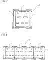
- two terminal parts 6 are provided, but depending on the number of female connectors, one terminal part 6 may be positioned and locked between the left end part 7 and the right end part 8 as shown in Fig. 7 .
- the number of terminal parts 6 positioned between the left end part 7 and the right end part 8 may be three or more.
- An example shown in Fig. 8 is an example in which four terminal parts 6 are positioned.
- the housing 10 of the terminal part 6 is provided with the openings on both sides in the arrangement direction D3. Accordingly, a size of the connector 4 can be further reduced.
- the terminal parts 6 have the same shape, but the present disclosure is not limited thereto. As shown in Figs. 9 and 10 , the terminal parts 6 may have different shapes in accordance with a shape of the female connector.
- a connector 4 is a connector 4 mountable on a substrate 2 and configured to be fitted to a counterpart connector, the connector 4 including: at least one terminal part 6, each of the at least one terminal part 6 including a terminal fitting 9 configured to be connected to the substrate 2, and a housing 10 that holds the terminal fitting 9 so as to allow the terminal fitting 9 to be fitted to the counterpart connector in a fitting direction D1; and a pair of end parts 7 and 8 including a first end part 7 and a second end part 8, the first end part 7 and the second end part 8 being configured to be arranged on the substrate 2 in an arrangement direction D3 perpendicular to the fitting direction D1 such that the at least one terminal part 6 is positioned between the first end part 7 and the second end part 8, in which each of the at least one terminal part 6 further includes a first locking portion 14, 15 provided in the housing 10 and configured to be locked to adjacent parts 6, 7, 8 on both sides in the arrangement direction D3, each of the first end part 7 and the second end part 8 includes a fixing portion 72, 82 configured
- the at least one terminal part 6 includes a plurality of terminal parts 6 configured to be arranged on the substrate 2 in the arrangement direction D3, and the first locking portion 14, 15 of each of the plurality of terminal parts 6 is configured to be locked to the first locking portion 14, 15 of another adjacent terminal part 6 in the arrangement direction D3.
- the housing 10 includes a support wall 11 that allows the terminal fitting 9 to penetrate therethrough to support the terminal fitting 9, a first cover wall 12 that is continuous with the support wall 11 and covers a first side of the terminal fitting 9 opposite to a second side facing the substrate 2, and a second cover wall 13 that is continuous with the support wall 11 and covers the second side of the terminal fitting 9, and both sides of the housing 10 in the arrangement direction D3 are opened.
- An electronic control unit 1 includes a substrate 2, an electronic part 3 mounted on the substrate 2, the above-described connector 4 which is mounted on the substrate 2, and a case 5 that accommodates the substrate 2, and a fitting surface of the connector 4 with respect to a counterpart connector is exposed from an opening 52A provided in the case 5.
- a terminal part 6 includes a terminal fitting 9 configured to be connected to a substrate 2, a housing 10 that holds the terminal fitting 9 so as to allow the terminal fitting 9 to be fitted to a counterpart connector in a fitting direction D1, and a first locking portion 14, 15 provided in the housing 10 and configured to be locked to adjacent parts on both sides in a direction D3 perpendicular to the fitting direction D1.
- a pair of end parts 7 and 8 includes a first end part 7 and a second end part 8.
- the first end part 7 and the second end part 8 are configured to be arranged on a substrate 2 such that at least one terminal part 6 is positioned between the first end part 7 and the second end part 8, each of the at least one terminal part 6 including a terminal fitting 9 configured to be connected to the substrate 2 and a housing 10 holding the terminal fitting 9, and each of the first end part 7 and the second end part 8 includes a fixing portion 72, 82 configured to be fixed to the substrate 2, and a second locking portion 73, 74, 83, 84 configured to be locked to an adjacent terminal part 6 among the at least one terminal part 6.
- the electronic control unit 1, the terminal part 6, and the pair of end parts 7 and 8 it is possible to easily cope with variations of the counterpart connector by changing the number and the shape of the terminal part 6 sandwiched between the pair of end parts 7 and 8.
- the fixing portions 72 and 82 to be fixed to the substrate 2 are provided on the pair of end parts 7 and 8 alone that position the terminal part 6 therebetween, and no fixing portions are provided on the terminal part 6. Therefore, even when there are a plurality of terminal parts 6, a size can be reduced.
- the housing 10 is opened on both sides in the arrangement direction D3, and thus the size can be further reduced.
Landscapes
- Connector Housings Or Holding Contact Members (AREA)
- Coupling Device And Connection With Printed Circuit (AREA)
Abstract
Description
- The present disclosure relates to a connector, an electronic control unit, a terminal part, and a pair of end parts.
- A connector for connection to an external device or the like may be mounted on a substrate. As such a connector mounted on the substrate, for example, a connector described in
Patent Literature 1 has been proposed.Patent Literature 1 discloses that connectors are mounted side by side, and the number of connectors is equal to the number of counterpart connectors to be connected to a substrate. - However, each connector in
Patent Literature 1 is provided with receiving portions on both sides in a width direction, and the receiving portions of the adjacent connectors are overlapped with each other, and are fixed to the substrate by passing a fixing fitting through both receiving portions. Therefore, when a plurality of connectors are mounted on the substrate, there is a problem that a size increases in the width direction. - Patent Literature 1:
JP-A-2015-041510 - The present disclosure has been made in view of the above circumstances, and an object of the present disclosure is to provide a connector, an electronic control unit, a terminal part, and a pair of end parts that are reduced in size while easily coping with variations of a counterpart connector.
- The present disclosure provides a connector mountable on a substrate and configured to be fitted to a counterpart connector, the connector including: at least one terminal part, each of the at least one terminal part including: a terminal fitting configured to be connected to the substrate; and a housing that holds the terminal fitting so as to allow the terminal fitting to be fitted to the counterpart connector in a fitting direction; and a pair of end parts including a first end part and a second end part, the first end part and the second end part being configured to be arranged on the substrate in an arrangement direction perpendicular to the fitting direction such that the at least one terminal part is positioned between the first end part and the second end part, wherein each of the at least one terminal part includes a first locking portion provided in the housing and configured to be locked to adjacent parts on both sides in the arrangement direction, wherein each of the first end part and the second end part includes: a fixing portion configured to be fixed to the substrate; and a second locking portion configured to be locked to the first locking portion of an adjacent terminal part in the arrangement direction among the at least one terminal part, and wherein the first end part, the at least one terminal part, and the second end part are connected while being arranged in this order on the substrate.
- The present disclosure provides an electronic control unit including: a substrate; an electronic part mounted on the substrate; the above-described connector, which is mounted on the substrate; and a case that accommodates the substrate, wherein a fitting surface of the connector with respect to a counterpart connector is exposed from an opening provided in the case.
- The present disclosure provides a terminal part including: a terminal fitting configured to be connected to a substrate; a housing that holds the terminal fitting so as to allow the terminal fitting to be fitted to a counterpart connector in a fitting direction; and a first locking portion provided in the housing and configured to be locked to adjacent parts on both sides in a direction perpendicular to the fitting direction.
- The present disclosure provides a pair of end parts including: a first end part; and a second end part, wherein the first end part and the second end part are configured to be arranged on a substrate such that at least one terminal part is positioned between the first end part and the second end part, each of the at least one terminal part including a terminal fitting configured to be connected to the substrate and a housing holding the terminal fitting, and wherein each of the first end part and the second end part includes: a fixing portion configured to be fixed to the substrate; and a second locking portion configured to be locked to an adjacent terminal part among the at least one terminal part.
- The present disclosure has been briefly described above. Details of the present disclosure will be further clarified by reading an aspect (hereinafter, referred to as an "embodiment") for implementing the invention to be described below with reference to the accompanying drawings.
-
-
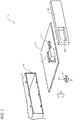
Fig. 1 is an exploded perspective view showing an electronic control unit according to an embodiment of the present disclosure; -
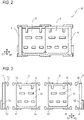
Fig. 2 is a front view of a connector constituting the electronic control unit shown inFig. 1 ; -
Fig. 3 is an exploded front view of the connector shown inFig. 2 ; -
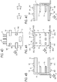
Fig. 4A to Fig. 4D are a front view, a left side view, a right side view, and a top view of a terminal part constituting the connector shown inFig. 2 , respectively; -
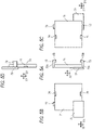
Fig. 5A to Fig. 5D are a front view, a left side view, a right side view, and a top view of a left end part constituting the connector shown inFig. 2 , respectively; -
Fig. 6A to Fig. 6D are a front view, a left side view, a right side view, and a top view of a right end part constituting the connector shown inFig. 2 , respectively; -
Fig. 7 is a front view of a connector according to another embodiment; -
Fig. 8 is a front view of a connector according to yet another embodiment; -
Fig. 9 is a front view of a connector according to still another embodiment; and -
Fig. 10 is an exploded front view of the connector shown inFig. 9 . - Specific embodiments according to the present disclosure will be described below with reference to the accompanying drawings.
- As shown in
Fig. 1 , anelectronic control unit 1 according to an embodiment includes asubstrate 2,electronic parts 3 mounted on thesubstrate 2, aconnector 4 mounted on thesubstrate 2, and a case 5 that accommodates the substrate. - The
substrate 2 is provided in a flat plate shape, and theelectronic parts 3 and theconnector 4 are mounted on an upper surface thereof. Theelectronic parts 3, andterminal fittings 9 to be described later constituting theconnector 4 are electrically connected to each other by a wiring pattern formed on thesubstrate 2 by printing or the like. - As shown in
Figs. 2 and 3 , theconnector 4 in the present embodiment includes twoterminal parts 6, and a left end part 7 (an example of a first end part) and a right end part 8 (an example of a second end part) which are a pair of end parts. Theseparts 6 to 8 are arranged on thesubstrate 2 along an arrangement direction D3 perpendicular to a fitting direction D1 of theconnector 4. More specifically, theleft end part 7, the twoterminal parts 6, and theright end part 8 are connected while being arranged in this order from a left side, which is one side in the arrangement direction D3, to a right side, which is the other side. - In the present embodiment, the two
terminal parts 6 have the same size and the same shape as each other. As shown inFig. 4 , theterminal part 6 includes theterminal fittings 9 to be connected to thesubstrate 2, and ahousing 10 holding theterminal fittings 9. Theterminal fitting 9 is formed in a substantially L-shape, and one end thereof is accommodated in thehousing 10, and the other end thereof protrudes outside thehousing 10, and is connectable to thesubstrate 2. The one end of the terminal fitting 9 accommodated in thehousing 10 is provided in a shape of a male terminal, and is capable of being fitted to a female terminal fitting of a female connector (not shown) as a counterpart connector. - The
housing 10 is made of an insulating material such as a synthetic resin. Thehousing 10 includessupport walls 11 that support the terminal fitting 9, an upper wall (a first cover wall) 12 that is continuous with thesupport walls 11 and covers a side of the terminal fitting 9 (an example of a first side of the terminal fitting 9) away from thesubstrate 2, and a lower wall (a second cover wall) 13 that is continuous with thesupport walls 11 and covers asubstrate 2 side of the terminal fitting 9 (an example of a second side of the terminal fitting 9). Thesupport walls 11 are provided perpendicular to the fitting direction D1 of the terminal fitting 9. Eachsupport wall 11 is formed with insertion holes (not shown) into which theterminal fittings 9 are inserted, respectively. - The
upper wall 12 is erected from an end portion of thesupport wall 11 on an upper side in an up-down direction D2 (the side away from the substrate 2) toward a female connector side in the fitting direction D1. The up-down direction D2 is a direction perpendicular to thesubstrate 2. Thelower wall 13 is erected from an end portion of thesupport wall 11 on a lower side in the up-down direction D2 (thesubstrate 2 side) toward the female connector side in the fitting direction D1. Thehousing 10 is not provided with a side wall, and is opened on both sides in the arrangement direction D3. - The
upper wall 12 and thelower wall 13 are each provided withlocking pairs parts 6 to 8 arranged adjacent on both sides in the arrangement direction D3. Thelocking pair 14 includes alocking arm 141 and alocking hole 142. Thelocking arm 141 and thelocking hole 142 are provided to be arranged in the arrangement direction D3. In the present embodiment, thelocking arm 141 is disposed on a left side in the arrangement direction D3, and thelocking hole 142 is disposed on a right side in the arrangement direction D3. Thelocking arm 141 includes anarm body 141A protruding from theupper wall 12 or thelower wall 13 toward the left side in the arrangement direction D3, and alocking projection 141B protruding from a tip of thearm body 141A. - The
locking pairs locking pair 14 is disposed on the female connector side (the one side) in the fitting direction D1, and thelocking pair 15 is disposed on the side (the other side) away from the female connector in the fitting direction D1. Thelocking pair 15 includes alocking arm 151 and alocking hole 152. Thelocking arm 151 and thelocking hole 152 are provided to be arranged in the arrangement direction D3. In the present embodiment, thelocking arm 151 is disposed on the left side in the arrangement direction D3, and thelocking hole 152 is disposed on the right side in the arrangement direction D3. Thelocking arm 151 includes anarm body 151A protruding from theupper wall 12 or thelower wall 12 toward the right side in the arrangement direction D3, and alocking projection 151B protruding from a tip of thearm body 151A. - As shown in
Fig. 2 , when the twoterminal parts 6 are arranged in the arrangement direction D3, the lockingprojection 141B provided on thelocking arm 141 of the rightterminal part 6 is fitted into thelocking hole 142 of the leftterminal part 6, and the twoterminal parts 6 are locked. The lockingprojection 151B provided on thelocking arm 151 of the leftterminal part 6 is fitted into thelocking hole 152 of the rightterminal part 6, and the twoterminal parts 6 are locked. - The
left end part 7 and theright end part 8 are arranged on thesubstrate 2 in the arrangement direction D3. The twoterminal parts 6 are positioned between theleft end part 7 and theright end part 8. As shown inFigs. 2 and 3 , theleft end part 7 is disposed on a left side of the twoterminal parts 6 in the arrangement direction D3, and is locked to a leftmost side of the twoterminal parts 6. As shown inFig. 5 , theleft end part 7 includes abody wall 71 that closes an opening of thehousing 10 of theterminal part 6 on the left side in the arrangement direction D3, a fixingportion 72 that is provided outside thebody wall 71 and is to be fixed to thesubstrate 2, and lockingarms 73 and lockingholes 74 as a second locking portion to be locked to the locking pairs 14 and 15 of the adjacentterminal part 6 on the right side in the arrangement direction D3. - The
body wall 71 is provided perpendicular to the arrangement direction D3. The fixingportion 72 includes a peg or a screw boss, and is to be fixed to thesubstrate 2. The lockingarms 73 and the locking holes 74 are provided to be arranged along the fitting direction D1. In the present embodiment, the locking holes 74 are disposed on the female connector side in the fitting direction D1, and the lockingarms 73 are disposed on the side away from the female connector in the fitting direction D1. The lockingarm 73 includes anarm body 73A protruding from an upper surface or a lower surface of thebody wall 71 toward the right side in the arrangement direction D3, and a lockingprojection 73B protruding from a tip of thearm body 73A. The locking holes 74 are provided on the upper surface and a left side surface of thebody wall 71. - The locking
projection 73B of the lockingarm 73 is fitted into thelocking hole 152 of the adjacentterminal part 6 on the right side in the arrangement direction D3. The lockingprojection 141B of thelocking arm 141 of the adjacentterminal part 6 on the right side in the arrangement direction D3 is fitted into the lockinghole 74. Accordingly, theterminal part 6 and theleft end part 7 are locked to each other. - As shown in
Figs. 2 and 3 , theright end part 8 is disposed on a right side of the twoterminal parts 6 in the arrangement direction D3, and is locked to a rightmost side of the twoterminal parts 6. As shown inFig. 6 , theright end part 8 includes abody wall 81 that closes an opening of thehousing 10 of theterminal part 6 on the right side in the arrangement direction D3, a fixingportion 82 that is provided outside thebody wall 81 and is to be fixed to thesubstrate 2, and lockingarms 83 and lockingholes 84 as a second locking portion to be locked to the locking pairs 14 and 15 of the adjacentterminal part 6 on the left side in the arrangement direction D3. - The
body wall 81 is provided perpendicular to the arrangement direction D3. The fixingportion 82 includes a peg or a screw boss, and is to be fixed to thesubstrate 2. The lockingarms 83 and the locking holes 84 are provided to be arranged along the fitting direction D1. In the present embodiment, the lockingarms 83 are disposed on the female connector side in the fitting direction D1, and the locking holes 84 are disposed on the side away from the female connector in the fitting direction D1. The lockingarm 83 includes anarm body 83A protruding from an upper surface or a lower surface of thebody wall 81 toward the left side in the arrangement direction D3, and a lockingprojection 83B protruding from a tip of thearm body 83A. The locking holes 84 are provided on the upper surface and a right side surface of thebody wall 81. - The locking
projection 83B of the lockingarm 83 is fitted into thelocking hole 142 of the adjacentterminal part 6 on the left side in the arrangement direction D3. The lockingprojection 151B of thelocking arm 151 of the adjacentterminal part 6 on the left side in the arrangement direction D3 is fitted into the lockinghole 84. Accordingly, theterminal part 6 and theright end part 8 are locked to each other. - According to the above configuration, as shown in
Fig. 2 , theleft end part 7, the twoterminal parts 6, and theright end part 8 are connected while being arranged in this order and arranged on thesubstrate 2, and the fixingportion 72 of theleft end part 7 and the fixingportion 82 of theright end part 8 are fixed to thesubstrate 2, so that theconnector 4 can be fixed. - As shown in
Fig. 1 , the case 5 includes acase body 51 in which the female connector side in the fitting direction D1 is opened, and afront cover 52 that closes an opening of thecase body 51. Thefront cover 52 is provided with anopening 52A, and theterminal fittings 9 of theconnector 4, that is, a fitting surface is exposed from theopening 52A. When the female connector is inserted into the case 5 through theopening 52A, the female connector and theconnector 4 are fitted and electrically connected. - According to the above embodiment, the fixing
portions substrate 2 are provided on theleft end part 7 and theright end part 8 alone that position theterminal part 6 therebetween, and the fixingportions terminal part 6. Therefore, even when there are a plurality ofterminal parts 6, a size can be reduced. In addition, according to theelectronic control unit 1, theterminal part 6, and the left andright end parts terminal part 6. - That is, according to the above embodiment, two
terminal parts 6 are provided, but depending on the number of female connectors, oneterminal part 6 may be positioned and locked between theleft end part 7 and theright end part 8 as shown inFig. 7 . - The number of
terminal parts 6 positioned between theleft end part 7 and theright end part 8 may be three or more. An example shown inFig. 8 is an example in which fourterminal parts 6 are positioned. - According to the above embodiment, the
housing 10 of theterminal part 6 is provided with the openings on both sides in the arrangement direction D3. Accordingly, a size of theconnector 4 can be further reduced. - The present disclosure is not limited to the above embodiment, and modifications, improvements, and the like can be made as appropriate. In addition, materials, shapes, dimensions, numbers, arrangement positions, and the like of components in the above embodiment are freely set and are not limited as long as the present disclosure can be achieved.
- In the above embodiment, the
terminal parts 6 have the same shape, but the present disclosure is not limited thereto. As shown inFigs. 9 and10 , theterminal parts 6 may have different shapes in accordance with a shape of the female connector. - A connector 4 according to an embodiment of the present disclosure is a connector 4 mountable on a substrate 2 and configured to be fitted to a counterpart connector, the connector 4 including: at least one terminal part 6, each of the at least one terminal part 6 including a terminal fitting 9 configured to be connected to the substrate 2, and a housing 10 that holds the terminal fitting 9 so as to allow the terminal fitting 9 to be fitted to the counterpart connector in a fitting direction D1; and a pair of end parts 7 and 8 including a first end part 7 and a second end part 8, the first end part 7 and the second end part 8 being configured to be arranged on the substrate 2 in an arrangement direction D3 perpendicular to the fitting direction D1 such that the at least one terminal part 6 is positioned between the first end part 7 and the second end part 8, in which each of the at least one terminal part 6 further includes a first locking portion 14, 15 provided in the housing 10 and configured to be locked to adjacent parts 6, 7, 8 on both sides in the arrangement direction D3, each of the first end part 7 and the second end part 8 includes a fixing portion 72, 82 configured to be fixed to the substrate 2, and a second locking portion 73, 74, 83, 84 configured to be locked to the first locking portion 14, 15 of an adjacent terminal part 6 in the arrangement direction D3 among the at least one terminal part 6, and the first end part 7, the at least one terminal part 6, and the second end part 8 are connected while being arranged in this order on the substrate 2.
- The at least one
terminal part 6 includes a plurality ofterminal parts 6 configured to be arranged on thesubstrate 2 in the arrangement direction D3, and thefirst locking portion terminal parts 6 is configured to be locked to thefirst locking portion terminal part 6 in the arrangement direction D3. - The
housing 10 includes asupport wall 11 that allows theterminal fitting 9 to penetrate therethrough to support theterminal fitting 9, afirst cover wall 12 that is continuous with thesupport wall 11 and covers a first side of theterminal fitting 9 opposite to a second side facing thesubstrate 2, and asecond cover wall 13 that is continuous with thesupport wall 11 and covers the second side of theterminal fitting 9, and both sides of thehousing 10 in the arrangement direction D3 are opened. - An
electronic control unit 1 according to an embodiment of the present disclosure includes asubstrate 2, anelectronic part 3 mounted on thesubstrate 2, the above-describedconnector 4 which is mounted on thesubstrate 2, and a case 5 that accommodates thesubstrate 2, and a fitting surface of theconnector 4 with respect to a counterpart connector is exposed from anopening 52A provided in the case 5. - A
terminal part 6 according to an embodiment of the present disclosure includes aterminal fitting 9 configured to be connected to asubstrate 2, ahousing 10 that holds theterminal fitting 9 so as to allow theterminal fitting 9 to be fitted to a counterpart connector in a fitting direction D1, and afirst locking portion housing 10 and configured to be locked to adjacent parts on both sides in a direction D3 perpendicular to the fitting direction D1. - A pair of
end parts first end part 7 and asecond end part 8. Thefirst end part 7 and thesecond end part 8 are configured to be arranged on asubstrate 2 such that at least oneterminal part 6 is positioned between thefirst end part 7 and thesecond end part 8, each of the at least oneterminal part 6 including aterminal fitting 9 configured to be connected to thesubstrate 2 and ahousing 10 holding theterminal fitting 9, and each of thefirst end part 7 and thesecond end part 8 includes a fixingportion substrate 2, and asecond locking portion terminal part 6 among the at least oneterminal part 6. - According to the
connector 4, theelectronic control unit 1, theterminal part 6, and the pair ofend parts terminal part 6 sandwiched between the pair ofend parts portions substrate 2 are provided on the pair ofend parts terminal part 6 therebetween, and no fixing portions are provided on theterminal part 6. Therefore, even when there are a plurality ofterminal parts 6, a size can be reduced. - The
housing 10 is opened on both sides in the arrangement direction D3, and thus the size can be further reduced. - According to the present disclosure, it is possible to provide a connector, an electronic control unit, a terminal part, and a pair of end parts that are reduced in size while easily coping with variations of a counterpart connector.
Claims (6)
- A connector (4) mountable on a substrate (2) and configured to be fitted to a counterpart connector, the connector (4) comprising:at least one terminal part (6), each of the at least one terminal part (6) comprising:a terminal fitting (9) configured to be connected to the substrate (2); anda housing (10) that holds the terminal fitting (9) so as to allow the terminal fitting (9) to be fitted to the counterpart connector in a fitting direction (D1); anda pair of end parts (7, 8) comprising a first end part (7) and a second end part (8), the first end part (7) and the second end part (8) being configured to be arranged on the substrate (2) in an arrangement direction (D3) perpendicular to the fitting direction (D1) such that the at least one terminal part (6) is positioned between the first end part (7) and the second end part (8),wherein each of the at least one terminal part (6) comprises a first locking portion (14, 15) provided in the housing (10) and configured to be locked to adjacent parts (6, 7, 8) on both sides in the arrangement direction (D3),wherein each of the first end part (7) and the second end part (8) comprises:a fixing portion (72, 82) configured to be fixed to the substrate (2); anda second locking portion (73, 74, 83, 84) configured to be locked to the first locking portion (14, 15) of an adjacent terminal part (6) in the arrangement direction (D3) among the at least one terminal part (6), andwherein the first end part (7), the at least one terminal part (6), and the second end part (8) are connected while being arranged in this order on the substrate (2).
- The connector (4) according to claim 1,wherein the at least one terminal part (6) comprises a plurality of terminal parts (6) configured to be arranged on the substrate (2) in the arrangement direction (D3), andwherein the first locking portion (14, 15) of each of the plurality of terminal parts (6) is configured to be locked to the first locking portion (14, 15) of another adjacent terminal part (6) in the arrangement direction (D3).
- The connector (4) according to claim 1 or 2,wherein the housing (10) comprises:a support wall (11) that allows the terminal fitting (9) to penetrate therethrough to support the terminal fitting (9);a first cover wall (12) that is continuous with the support wall (11) and covers a first side of the terminal fitting (9) opposite to a second side facing the substrate (2); anda second cover wall (13) that is continuous with the support wall (11) and covers the second side of the terminal fitting (9), andwherein both sides of the housing (10) in the arrangement direction (D3) are opened.
- An electronic control unit (1) comprising:a substrate (2);an electronic part (3) mounted on the substrate (2);the connector (4) according to any one of claims 1 to 3, which is mounted on the substrate (2); anda case (5) that accommodates the substrate (2),wherein a fitting surface of the connector (4) with respect to a counterpart connector is exposed from an opening (52A) provided in the case (5).
- A terminal part (6) comprising:a terminal fitting (9) configured to be connected to a substrate (2);a housing (10) that holds the terminal fitting so as to allow the terminal fitting (9) to be fitted to a counterpart connector in a fitting direction (D1); anda first locking portion (14, 15) provided in the housing (10) and configured to be locked to adjacent parts (6, 7, 8) on both sides in a direction (D3) perpendicular to the fitting direction (D1).
- A pair of end parts (7, 8) comprising:a first end part (7); anda second end part (8),wherein the first end part (7) and the second end part (8) are configured to be arranged on a substrate (2) such that at least one terminal part (6) is positioned between the first end part (7) and the second end part (8), each of the at least one terminal part (6) comprising a terminal fitting (9) configured to be connected to the substrate (2) and a housing (10) holding the terminal fitting (9), andwherein each of the first end part (7) and the second end part (8) comprises:a fixing portion (72, 82) configured to be fixed to the substrate (2); anda second locking portion (73, 74, 83, 84) configured to be locked to an adjacent terminal part (6) among the at least one terminal part (6).
Applications Claiming Priority (1)
| Application Number | Priority Date | Filing Date | Title |
|---|---|---|---|
| JP2021082622A JP7364620B2 (en) | 2021-05-14 | 2021-05-14 | Connectors, electronic control units, terminal parts and a pair of end parts |
Publications (2)
| Publication Number | Publication Date |
|---|---|
| EP4089848A1 true EP4089848A1 (en) | 2022-11-16 |
| EP4089848B1 EP4089848B1 (en) | 2024-09-11 |
Family
ID=81327227
Family Applications (1)
| Application Number | Title | Priority Date | Filing Date |
|---|---|---|---|
| EP22168406.1A Active EP4089848B1 (en) | 2021-05-14 | 2022-04-14 | Connector, electronic control unit, terminal part, and pair of end parts |
Country Status (4)
| Country | Link |
|---|---|
| US (1) | US20220407253A1 (en) |
| EP (1) | EP4089848B1 (en) |
| JP (1) | JP7364620B2 (en) |
| CN (1) | CN115347386A (en) |
Citations (2)
| Publication number | Priority date | Publication date | Assignee | Title |
|---|---|---|---|---|
| US4790763A (en) * | 1986-04-22 | 1988-12-13 | Amp Incorporated | Programmable modular connector assembly |
| JP2015041510A (en) | 2013-08-22 | 2015-03-02 | 住友電装株式会社 | Connector for printed board |
Family Cites Families (8)
| Publication number | Priority date | Publication date | Assignee | Title |
|---|---|---|---|---|
| JPS504705Y1 (en) * | 1970-09-10 | 1975-02-07 | ||
| JPS51162972U (en) * | 1975-06-19 | 1976-12-25 | ||
| JPS6075979U (en) * | 1983-10-31 | 1985-05-28 | 日本電気ホームエレクトロニクス株式会社 | connection plug |
| JPH0799706B2 (en) * | 1986-09-15 | 1995-10-25 | アンプ インコーポレーテッド | Modular connector |
| US5368491A (en) * | 1993-12-17 | 1994-11-29 | The Whitaker Corporation | High density electrical connector |
| JP5853985B2 (en) * | 2013-04-05 | 2016-02-09 | 株式会社オートネットワーク技術研究所 | connector |
| JP6576886B2 (en) * | 2016-08-09 | 2019-09-18 | 日立オートモティブシステムズ株式会社 | Board connector and battery control device including the same |
| KR102373471B1 (en) * | 2018-06-29 | 2022-03-10 | 주식회사 엘지에너지솔루션 | Expandable connector assembly |
-
2021
- 2021-05-14 JP JP2021082622A patent/JP7364620B2/en active Active
-
2022
- 2022-04-13 CN CN202210386777.0A patent/CN115347386A/en active Pending
- 2022-04-14 EP EP22168406.1A patent/EP4089848B1/en active Active
- 2022-05-14 US US17/744,626 patent/US20220407253A1/en not_active Abandoned
Patent Citations (2)
| Publication number | Priority date | Publication date | Assignee | Title |
|---|---|---|---|---|
| US4790763A (en) * | 1986-04-22 | 1988-12-13 | Amp Incorporated | Programmable modular connector assembly |
| JP2015041510A (en) | 2013-08-22 | 2015-03-02 | 住友電装株式会社 | Connector for printed board |
Also Published As
| Publication number | Publication date |
|---|---|
| EP4089848B1 (en) | 2024-09-11 |
| CN115347386A (en) | 2022-11-15 |
| US20220407253A1 (en) | 2022-12-22 |
| JP7364620B2 (en) | 2023-10-18 |
| JP2022175867A (en) | 2022-11-25 |
Similar Documents
| Publication | Publication Date | Title |
|---|---|---|
| JP6074289B2 (en) | Female connector and card edge connector | |
| CN102185194B (en) | Electrical connector having contact modules | |
| US5772452A (en) | Connector for a circuit board | |
| CN102640363B (en) | Plug and socket connector arrangement with first and second plugs and mating plugs | |
| WO2008050665A1 (en) | Connector | |
| US9318858B2 (en) | Receptacle connector, plug connector and connector assembly | |
| CN110277659B (en) | Connecting piece and socket | |
| US6302744B1 (en) | Connector system with polarizing key mechanism | |
| US4940417A (en) | Connector device with fitting adjustment mechanism | |
| TW201803218A (en) | Surface mounting type connector | |
| US12142863B2 (en) | Branch connector having shorting plate connected to a pair of terminal fittings | |
| EP3799218B1 (en) | Connector | |
| TWI458185B (en) | Connector assembly having a noise-reducing contact pattern | |
| EP4089848B1 (en) | Connector, electronic control unit, terminal part, and pair of end parts | |
| WO2006134690A1 (en) | Electric junction box | |
| KR20180051950A (en) | Elctronic control device | |
| WO2010073397A1 (en) | Input/output unit | |
| KR20080076901A (en) | Electrical connector | |
| JP2007287519A (en) | Connection device | |
| JP7480073B2 (en) | Connectors with insert-molded terminals | |
| JP7468457B2 (en) | Flexible Cable Connectors | |
| TW202406239A (en) | Floating electrical connector | |
| JP3126066U (en) | Receptacle connector plug | |
| JP7806114B2 (en) | Printed Circuit Board (PCB) Housings and PCB Assemblies | |
| EP4568024A2 (en) | Reliable high speed connector with integrated power |
Legal Events
| Date | Code | Title | Description |
|---|---|---|---|
| PUAI | Public reference made under article 153(3) epc to a published international application that has entered the european phase |
Free format text: ORIGINAL CODE: 0009012 |
|
| STAA | Information on the status of an ep patent application or granted ep patent |
Free format text: STATUS: REQUEST FOR EXAMINATION WAS MADE |
|
| 17P | Request for examination filed |
Effective date: 20220414 |
|
| AK | Designated contracting states |
Kind code of ref document: A1 Designated state(s): AL AT BE BG CH CY CZ DE DK EE ES FI FR GB GR HR HU IE IS IT LI LT LU LV MC MK MT NL NO PL PT RO RS SE SI SK SM TR |
|
| RAP3 | Party data changed (applicant data changed or rights of an application transferred) |
Owner name: YAZAKI CORPORATION |
|
| GRAP | Despatch of communication of intention to grant a patent |
Free format text: ORIGINAL CODE: EPIDOSNIGR1 |
|
| STAA | Information on the status of an ep patent application or granted ep patent |
Free format text: STATUS: GRANT OF PATENT IS INTENDED |
|
| GRAS | Grant fee paid |
Free format text: ORIGINAL CODE: EPIDOSNIGR3 |
|
| INTG | Intention to grant announced |
Effective date: 20240709 |
|
| GRAA | (expected) grant |
Free format text: ORIGINAL CODE: 0009210 |
|
| STAA | Information on the status of an ep patent application or granted ep patent |
Free format text: STATUS: THE PATENT HAS BEEN GRANTED |
|
| AK | Designated contracting states |
Kind code of ref document: B1 Designated state(s): AL AT BE BG CH CY CZ DE DK EE ES FI FR GB GR HR HU IE IS IT LI LT LU LV MC MK MT NL NO PL PT RO RS SE SI SK SM TR |
|
| REG | Reference to a national code |
Ref country code: GB Ref legal event code: FG4D |
|
| REG | Reference to a national code |
Ref country code: CH Ref legal event code: EP |
|
| REG | Reference to a national code |
Ref country code: DE Ref legal event code: R096 Ref document number: 602022005962 Country of ref document: DE |
|
| REG | Reference to a national code |
Ref country code: IE Ref legal event code: FG4D |
|
| REG | Reference to a national code |
Ref country code: LT Ref legal event code: MG9D |
|
| PG25 | Lapsed in a contracting state [announced via postgrant information from national office to epo] |
Ref country code: NO Free format text: LAPSE BECAUSE OF FAILURE TO SUBMIT A TRANSLATION OF THE DESCRIPTION OR TO PAY THE FEE WITHIN THE PRESCRIBED TIME-LIMIT Effective date: 20241211 |
|
| REG | Reference to a national code |
Ref country code: NL Ref legal event code: MP Effective date: 20240911 |
|
| PG25 | Lapsed in a contracting state [announced via postgrant information from national office to epo] |
Ref country code: GR Free format text: LAPSE BECAUSE OF FAILURE TO SUBMIT A TRANSLATION OF THE DESCRIPTION OR TO PAY THE FEE WITHIN THE PRESCRIBED TIME-LIMIT Effective date: 20241212 Ref country code: FI Free format text: LAPSE BECAUSE OF FAILURE TO SUBMIT A TRANSLATION OF THE DESCRIPTION OR TO PAY THE FEE WITHIN THE PRESCRIBED TIME-LIMIT Effective date: 20240911 |
|
| PG25 | Lapsed in a contracting state [announced via postgrant information from national office to epo] |
Ref country code: BG Free format text: LAPSE BECAUSE OF FAILURE TO SUBMIT A TRANSLATION OF THE DESCRIPTION OR TO PAY THE FEE WITHIN THE PRESCRIBED TIME-LIMIT Effective date: 20240911 |
|
| PG25 | Lapsed in a contracting state [announced via postgrant information from national office to epo] |
Ref country code: LV Free format text: LAPSE BECAUSE OF FAILURE TO SUBMIT A TRANSLATION OF THE DESCRIPTION OR TO PAY THE FEE WITHIN THE PRESCRIBED TIME-LIMIT Effective date: 20240911 |
|
| PG25 | Lapsed in a contracting state [announced via postgrant information from national office to epo] |
Ref country code: HR Free format text: LAPSE BECAUSE OF FAILURE TO SUBMIT A TRANSLATION OF THE DESCRIPTION OR TO PAY THE FEE WITHIN THE PRESCRIBED TIME-LIMIT Effective date: 20240911 |
|
| PG25 | Lapsed in a contracting state [announced via postgrant information from national office to epo] |
Ref country code: ES Free format text: LAPSE BECAUSE OF FAILURE TO SUBMIT A TRANSLATION OF THE DESCRIPTION OR TO PAY THE FEE WITHIN THE PRESCRIBED TIME-LIMIT Effective date: 20240911 Ref country code: RS Free format text: LAPSE BECAUSE OF FAILURE TO SUBMIT A TRANSLATION OF THE DESCRIPTION OR TO PAY THE FEE WITHIN THE PRESCRIBED TIME-LIMIT Effective date: 20241211 |
|
| PG25 | Lapsed in a contracting state [announced via postgrant information from national office to epo] |
Ref country code: RS Free format text: LAPSE BECAUSE OF FAILURE TO SUBMIT A TRANSLATION OF THE DESCRIPTION OR TO PAY THE FEE WITHIN THE PRESCRIBED TIME-LIMIT Effective date: 20241211 Ref country code: NO Free format text: LAPSE BECAUSE OF FAILURE TO SUBMIT A TRANSLATION OF THE DESCRIPTION OR TO PAY THE FEE WITHIN THE PRESCRIBED TIME-LIMIT Effective date: 20241211 Ref country code: LV Free format text: LAPSE BECAUSE OF FAILURE TO SUBMIT A TRANSLATION OF THE DESCRIPTION OR TO PAY THE FEE WITHIN THE PRESCRIBED TIME-LIMIT Effective date: 20240911 Ref country code: HR Free format text: LAPSE BECAUSE OF FAILURE TO SUBMIT A TRANSLATION OF THE DESCRIPTION OR TO PAY THE FEE WITHIN THE PRESCRIBED TIME-LIMIT Effective date: 20240911 Ref country code: GR Free format text: LAPSE BECAUSE OF FAILURE TO SUBMIT A TRANSLATION OF THE DESCRIPTION OR TO PAY THE FEE WITHIN THE PRESCRIBED TIME-LIMIT Effective date: 20241212 Ref country code: FI Free format text: LAPSE BECAUSE OF FAILURE TO SUBMIT A TRANSLATION OF THE DESCRIPTION OR TO PAY THE FEE WITHIN THE PRESCRIBED TIME-LIMIT Effective date: 20240911 Ref country code: ES Free format text: LAPSE BECAUSE OF FAILURE TO SUBMIT A TRANSLATION OF THE DESCRIPTION OR TO PAY THE FEE WITHIN THE PRESCRIBED TIME-LIMIT Effective date: 20240911 Ref country code: BG Free format text: LAPSE BECAUSE OF FAILURE TO SUBMIT A TRANSLATION OF THE DESCRIPTION OR TO PAY THE FEE WITHIN THE PRESCRIBED TIME-LIMIT Effective date: 20240911 |
|
| REG | Reference to a national code |
Ref country code: AT Ref legal event code: MK05 Ref document number: 1723542 Country of ref document: AT Kind code of ref document: T Effective date: 20240911 |
|
| PG25 | Lapsed in a contracting state [announced via postgrant information from national office to epo] |
Ref country code: NL Free format text: LAPSE BECAUSE OF FAILURE TO SUBMIT A TRANSLATION OF THE DESCRIPTION OR TO PAY THE FEE WITHIN THE PRESCRIBED TIME-LIMIT Effective date: 20240911 |
|
| PG25 | Lapsed in a contracting state [announced via postgrant information from national office to epo] |
Ref country code: IS Free format text: LAPSE BECAUSE OF FAILURE TO SUBMIT A TRANSLATION OF THE DESCRIPTION OR TO PAY THE FEE WITHIN THE PRESCRIBED TIME-LIMIT Effective date: 20250111 Ref country code: PT Free format text: LAPSE BECAUSE OF FAILURE TO SUBMIT A TRANSLATION OF THE DESCRIPTION OR TO PAY THE FEE WITHIN THE PRESCRIBED TIME-LIMIT Effective date: 20250113 |
|
| PG25 | Lapsed in a contracting state [announced via postgrant information from national office to epo] |
Ref country code: RO Free format text: LAPSE BECAUSE OF FAILURE TO SUBMIT A TRANSLATION OF THE DESCRIPTION OR TO PAY THE FEE WITHIN THE PRESCRIBED TIME-LIMIT Effective date: 20240911 Ref country code: SM Free format text: LAPSE BECAUSE OF FAILURE TO SUBMIT A TRANSLATION OF THE DESCRIPTION OR TO PAY THE FEE WITHIN THE PRESCRIBED TIME-LIMIT Effective date: 20240911 |
|
| PG25 | Lapsed in a contracting state [announced via postgrant information from national office to epo] |
Ref country code: EE Free format text: LAPSE BECAUSE OF FAILURE TO SUBMIT A TRANSLATION OF THE DESCRIPTION OR TO PAY THE FEE WITHIN THE PRESCRIBED TIME-LIMIT Effective date: 20240911 Ref country code: AT Free format text: LAPSE BECAUSE OF FAILURE TO SUBMIT A TRANSLATION OF THE DESCRIPTION OR TO PAY THE FEE WITHIN THE PRESCRIBED TIME-LIMIT Effective date: 20240911 |
|
| PG25 | Lapsed in a contracting state [announced via postgrant information from national office to epo] |
Ref country code: CZ Free format text: LAPSE BECAUSE OF FAILURE TO SUBMIT A TRANSLATION OF THE DESCRIPTION OR TO PAY THE FEE WITHIN THE PRESCRIBED TIME-LIMIT Effective date: 20240911 Ref country code: PL Free format text: LAPSE BECAUSE OF FAILURE TO SUBMIT A TRANSLATION OF THE DESCRIPTION OR TO PAY THE FEE WITHIN THE PRESCRIBED TIME-LIMIT Effective date: 20240911 |
|
| PG25 | Lapsed in a contracting state [announced via postgrant information from national office to epo] |
Ref country code: SK Free format text: LAPSE BECAUSE OF FAILURE TO SUBMIT A TRANSLATION OF THE DESCRIPTION OR TO PAY THE FEE WITHIN THE PRESCRIBED TIME-LIMIT Effective date: 20240911 Ref country code: IT Free format text: LAPSE BECAUSE OF FAILURE TO SUBMIT A TRANSLATION OF THE DESCRIPTION OR TO PAY THE FEE WITHIN THE PRESCRIBED TIME-LIMIT Effective date: 20240911 |
|
| REG | Reference to a national code |
Ref country code: DE Ref legal event code: R097 Ref document number: 602022005962 Country of ref document: DE |
|
| PGFP | Annual fee paid to national office [announced via postgrant information from national office to epo] |
Ref country code: DE Payment date: 20250305 Year of fee payment: 4 |
|
| PG25 | Lapsed in a contracting state [announced via postgrant information from national office to epo] |
Ref country code: DK Free format text: LAPSE BECAUSE OF FAILURE TO SUBMIT A TRANSLATION OF THE DESCRIPTION OR TO PAY THE FEE WITHIN THE PRESCRIBED TIME-LIMIT Effective date: 20240911 |
|
| PLBE | No opposition filed within time limit |
Free format text: ORIGINAL CODE: 0009261 |
|
| STAA | Information on the status of an ep patent application or granted ep patent |
Free format text: STATUS: NO OPPOSITION FILED WITHIN TIME LIMIT |
|
| 26N | No opposition filed |
Effective date: 20250612 |
|
| PG25 | Lapsed in a contracting state [announced via postgrant information from national office to epo] |
Ref country code: SE Free format text: LAPSE BECAUSE OF FAILURE TO SUBMIT A TRANSLATION OF THE DESCRIPTION OR TO PAY THE FEE WITHIN THE PRESCRIBED TIME-LIMIT Effective date: 20240911 |
|
| REG | Reference to a national code |
Ref country code: CH Ref legal event code: H13 Free format text: ST27 STATUS EVENT CODE: U-0-0-H10-H13 (AS PROVIDED BY THE NATIONAL OFFICE) Effective date: 20251125 |
|
| PG25 | Lapsed in a contracting state [announced via postgrant information from national office to epo] |
Ref country code: LU Free format text: LAPSE BECAUSE OF NON-PAYMENT OF DUE FEES Effective date: 20250414 |
|
| PG25 | Lapsed in a contracting state [announced via postgrant information from national office to epo] |
Ref country code: MC Free format text: LAPSE BECAUSE OF FAILURE TO SUBMIT A TRANSLATION OF THE DESCRIPTION OR TO PAY THE FEE WITHIN THE PRESCRIBED TIME-LIMIT Effective date: 20240911 |
|
| REG | Reference to a national code |
Ref country code: BE Ref legal event code: MM Effective date: 20250430 |
|
| PG25 | Lapsed in a contracting state [announced via postgrant information from national office to epo] |
Ref country code: FR Free format text: LAPSE BECAUSE OF NON-PAYMENT OF DUE FEES Effective date: 20250430 |
|
| PG25 | Lapsed in a contracting state [announced via postgrant information from national office to epo] |
Ref country code: BE Free format text: LAPSE BECAUSE OF NON-PAYMENT OF DUE FEES Effective date: 20250430 |
|
| PG25 | Lapsed in a contracting state [announced via postgrant information from national office to epo] |
Ref country code: CH Free format text: LAPSE BECAUSE OF NON-PAYMENT OF DUE FEES Effective date: 20250430 |
|
| PG25 | Lapsed in a contracting state [announced via postgrant information from national office to epo] |
Ref country code: IE Free format text: LAPSE BECAUSE OF NON-PAYMENT OF DUE FEES Effective date: 20250414 |