EP4089759A1 - Pole piece, electrochemical device, and electronic device - Google Patents
Pole piece, electrochemical device, and electronic device Download PDFInfo
- Publication number
- EP4089759A1 EP4089759A1 EP22710473.4A EP22710473A EP4089759A1 EP 4089759 A1 EP4089759 A1 EP 4089759A1 EP 22710473 A EP22710473 A EP 22710473A EP 4089759 A1 EP4089759 A1 EP 4089759A1
- Authority
- EP
- European Patent Office
- Prior art keywords
- area
- electrode plate
- functional
- thickness
- coating
- Prior art date
- Legal status (The legal status is an assumption and is not a legal conclusion. Google has not performed a legal analysis and makes no representation as to the accuracy of the status listed.)
- Pending
Links
- 238000000576 coating method Methods 0.000 claims abstract description 111
- 239000011248 coating agent Substances 0.000 claims abstract description 109
- 239000011888 foil Substances 0.000 claims description 11
- 230000003247 decreasing effect Effects 0.000 claims description 9
- 230000007704 transition Effects 0.000 abstract description 12
- 230000000694 effects Effects 0.000 abstract description 4
- 230000001351 cycling effect Effects 0.000 abstract description 2
- 239000013543 active substance Substances 0.000 description 14
- 230000000052 comparative effect Effects 0.000 description 14
- OKTJSMMVPCPJKN-UHFFFAOYSA-N Carbon Chemical compound [C] OKTJSMMVPCPJKN-UHFFFAOYSA-N 0.000 description 7
- 238000004519 manufacturing process Methods 0.000 description 6
- 239000000463 material Substances 0.000 description 6
- -1 polytetrafluoroethylene Polymers 0.000 description 6
- RYGMFSIKBFXOCR-UHFFFAOYSA-N Copper Chemical compound [Cu] RYGMFSIKBFXOCR-UHFFFAOYSA-N 0.000 description 4
- 229910052782 aluminium Inorganic materials 0.000 description 4
- XAGFODPZIPBFFR-UHFFFAOYSA-N aluminium Chemical compound [Al] XAGFODPZIPBFFR-UHFFFAOYSA-N 0.000 description 4
- 239000011889 copper foil Substances 0.000 description 4
- 239000011267 electrode slurry Substances 0.000 description 4
- 229910002804 graphite Inorganic materials 0.000 description 4
- 239000010439 graphite Substances 0.000 description 4
- 238000000034 method Methods 0.000 description 4
- 229920002981 polyvinylidene fluoride Polymers 0.000 description 4
- 238000003825 pressing Methods 0.000 description 4
- HBBGRARXTFLTSG-UHFFFAOYSA-N Lithium ion Chemical compound [Li+] HBBGRARXTFLTSG-UHFFFAOYSA-N 0.000 description 3
- 239000002033 PVDF binder Substances 0.000 description 3
- 239000011230 binding agent Substances 0.000 description 3
- 238000004140 cleaning Methods 0.000 description 3
- 239000006258 conductive agent Substances 0.000 description 3
- 238000001035 drying Methods 0.000 description 3
- 229910000625 lithium cobalt oxide Inorganic materials 0.000 description 3
- 229910001416 lithium ion Inorganic materials 0.000 description 3
- BFZPBUKRYWOWDV-UHFFFAOYSA-N lithium;oxido(oxo)cobalt Chemical compound [Li+].[O-][Co]=O BFZPBUKRYWOWDV-UHFFFAOYSA-N 0.000 description 3
- 238000005096 rolling process Methods 0.000 description 3
- 229920003048 styrene butadiene rubber Polymers 0.000 description 3
- XUIMIQQOPSSXEZ-UHFFFAOYSA-N Silicon Chemical compound [Si] XUIMIQQOPSSXEZ-UHFFFAOYSA-N 0.000 description 2
- HMDDXIMCDZRSNE-UHFFFAOYSA-N [C].[Si] Chemical compound [C].[Si] HMDDXIMCDZRSNE-UHFFFAOYSA-N 0.000 description 2
- 229910052799 carbon Inorganic materials 0.000 description 2
- 239000000470 constituent Substances 0.000 description 2
- 238000007796 conventional method Methods 0.000 description 2
- 238000010586 diagram Methods 0.000 description 2
- 239000002931 mesocarbon microbead Substances 0.000 description 2
- 229910052751 metal Inorganic materials 0.000 description 2
- 239000002184 metal Substances 0.000 description 2
- 229910021645 metal ion Inorganic materials 0.000 description 2
- VNWKTOKETHGBQD-UHFFFAOYSA-N methane Chemical compound C VNWKTOKETHGBQD-UHFFFAOYSA-N 0.000 description 2
- 229910052710 silicon Inorganic materials 0.000 description 2
- 239000010703 silicon Substances 0.000 description 2
- 238000012360 testing method Methods 0.000 description 2
- 229920000049 Carbon (fiber) Polymers 0.000 description 1
- 229920002153 Hydroxypropyl cellulose Polymers 0.000 description 1
- SECXISVLQFMRJM-UHFFFAOYSA-N N-Methylpyrrolidone Chemical compound CN1CCCC1=O SECXISVLQFMRJM-UHFFFAOYSA-N 0.000 description 1
- 239000004677 Nylon Substances 0.000 description 1
- 239000004698 Polyethylene Substances 0.000 description 1
- 239000004743 Polypropylene Substances 0.000 description 1
- 239000004372 Polyvinyl alcohol Substances 0.000 description 1
- KFDQGLPGKXUTMZ-UHFFFAOYSA-N [Mn].[Co].[Ni] Chemical compound [Mn].[Co].[Ni] KFDQGLPGKXUTMZ-UHFFFAOYSA-N 0.000 description 1
- 239000006230 acetylene black Substances 0.000 description 1
- NIXOWILDQLNWCW-UHFFFAOYSA-N acrylic acid group Chemical group C(C=C)(=O)O NIXOWILDQLNWCW-UHFFFAOYSA-N 0.000 description 1
- 229910021383 artificial graphite Inorganic materials 0.000 description 1
- 239000003990 capacitor Substances 0.000 description 1
- 239000004917 carbon fiber Substances 0.000 description 1
- 239000005466 carboxylated polyvinylchloride Substances 0.000 description 1
- 239000008367 deionised water Substances 0.000 description 1
- 229910021641 deionized water Inorganic materials 0.000 description 1
- 238000013461 design Methods 0.000 description 1
- 238000011161 development Methods 0.000 description 1
- 229920005994 diacetyl cellulose Polymers 0.000 description 1
- QHGJSLXSVXVKHZ-UHFFFAOYSA-N dilithium;dioxido(dioxo)manganese Chemical compound [Li+].[Li+].[O-][Mn]([O-])(=O)=O QHGJSLXSVXVKHZ-UHFFFAOYSA-N 0.000 description 1
- 238000012983 electrochemical energy storage Methods 0.000 description 1
- 238000003487 electrochemical reaction Methods 0.000 description 1
- 238000004146 energy storage Methods 0.000 description 1
- 239000003822 epoxy resin Substances 0.000 description 1
- 125000000219 ethylidene group Chemical group [H]C(=[*])C([H])([H])[H] 0.000 description 1
- 238000002474 experimental method Methods 0.000 description 1
- 230000002349 favourable effect Effects 0.000 description 1
- 239000000446 fuel Substances 0.000 description 1
- 238000007755 gap coating Methods 0.000 description 1
- 229910021385 hard carbon Inorganic materials 0.000 description 1
- 239000001863 hydroxypropyl cellulose Substances 0.000 description 1
- 235000010977 hydroxypropyl cellulose Nutrition 0.000 description 1
- 230000002427 irreversible effect Effects 0.000 description 1
- 239000003273 ketjen black Substances 0.000 description 1
- GELKBWJHTRAYNV-UHFFFAOYSA-K lithium iron phosphate Chemical compound [Li+].[Fe+2].[O-]P([O-])([O-])=O GELKBWJHTRAYNV-UHFFFAOYSA-K 0.000 description 1
- 238000003754 machining Methods 0.000 description 1
- 238000012986 modification Methods 0.000 description 1
- 230000004048 modification Effects 0.000 description 1
- 229910021382 natural graphite Inorganic materials 0.000 description 1
- 229920001778 nylon Polymers 0.000 description 1
- 229920000647 polyepoxide Polymers 0.000 description 1
- 229920000573 polyethylene Polymers 0.000 description 1
- 229920000642 polymer Polymers 0.000 description 1
- 229920001155 polypropylene Polymers 0.000 description 1
- 229920001343 polytetrafluoroethylene Polymers 0.000 description 1
- 239000004810 polytetrafluoroethylene Substances 0.000 description 1
- 229920002635 polyurethane Polymers 0.000 description 1
- 239000004814 polyurethane Substances 0.000 description 1
- 229920002451 polyvinyl alcohol Polymers 0.000 description 1
- 229920000915 polyvinyl chloride Polymers 0.000 description 1
- 239000004800 polyvinyl chloride Substances 0.000 description 1
- 229920002620 polyvinyl fluoride Polymers 0.000 description 1
- 229920000973 polyvinylchloride carboxylated Polymers 0.000 description 1
- 229920000036 polyvinylpyrrolidone Polymers 0.000 description 1
- 239000001267 polyvinylpyrrolidone Substances 0.000 description 1
- 235000013855 polyvinylpyrrolidone Nutrition 0.000 description 1
- 238000011160 research Methods 0.000 description 1
- 239000002002 slurry Substances 0.000 description 1
- 229910021384 soft carbon Inorganic materials 0.000 description 1
- 238000012795 verification Methods 0.000 description 1
- XLYOFNOQVPJJNP-UHFFFAOYSA-N water Chemical compound O XLYOFNOQVPJJNP-UHFFFAOYSA-N 0.000 description 1
- 230000003313 weakening effect Effects 0.000 description 1
- 238000003466 welding Methods 0.000 description 1
Images

Classifications
-
- H—ELECTRICITY
- H01—ELECTRIC ELEMENTS
- H01M—PROCESSES OR MEANS, e.g. BATTERIES, FOR THE DIRECT CONVERSION OF CHEMICAL ENERGY INTO ELECTRICAL ENERGY
- H01M4/00—Electrodes
- H01M4/02—Electrodes composed of, or comprising, active material
- H01M4/13—Electrodes for accumulators with non-aqueous electrolyte, e.g. for lithium-accumulators; Processes of manufacture thereof
-
- H—ELECTRICITY
- H01—ELECTRIC ELEMENTS
- H01M—PROCESSES OR MEANS, e.g. BATTERIES, FOR THE DIRECT CONVERSION OF CHEMICAL ENERGY INTO ELECTRICAL ENERGY
- H01M4/00—Electrodes
- H01M4/02—Electrodes composed of, or comprising, active material
- H01M4/64—Carriers or collectors
- H01M4/66—Selection of materials
- H01M4/665—Composites
- H01M4/667—Composites in the form of layers, e.g. coatings
-
- H—ELECTRICITY
- H01—ELECTRIC ELEMENTS
- H01M—PROCESSES OR MEANS, e.g. BATTERIES, FOR THE DIRECT CONVERSION OF CHEMICAL ENERGY INTO ELECTRICAL ENERGY
- H01M4/00—Electrodes
- H01M4/02—Electrodes composed of, or comprising, active material
- H01M4/04—Processes of manufacture in general
- H01M4/043—Processes of manufacture in general involving compressing or compaction
-
- H—ELECTRICITY
- H01—ELECTRIC ELEMENTS
- H01G—CAPACITORS; CAPACITORS, RECTIFIERS, DETECTORS, SWITCHING DEVICES, LIGHT-SENSITIVE OR TEMPERATURE-SENSITIVE DEVICES OF THE ELECTROLYTIC TYPE
- H01G11/00—Hybrid capacitors, i.e. capacitors having different positive and negative electrodes; Electric double-layer [EDL] capacitors; Processes for the manufacture thereof or of parts thereof
- H01G11/22—Electrodes
- H01G11/26—Electrodes characterised by their structure, e.g. multi-layered, porosity or surface features
- H01G11/28—Electrodes characterised by their structure, e.g. multi-layered, porosity or surface features arranged or disposed on a current collector; Layers or phases between electrodes and current collectors, e.g. adhesives
-
- H—ELECTRICITY
- H01—ELECTRIC ELEMENTS
- H01G—CAPACITORS; CAPACITORS, RECTIFIERS, DETECTORS, SWITCHING DEVICES, LIGHT-SENSITIVE OR TEMPERATURE-SENSITIVE DEVICES OF THE ELECTROLYTIC TYPE
- H01G11/00—Hybrid capacitors, i.e. capacitors having different positive and negative electrodes; Electric double-layer [EDL] capacitors; Processes for the manufacture thereof or of parts thereof
- H01G11/66—Current collectors
- H01G11/70—Current collectors characterised by their structure
-
- H—ELECTRICITY
- H01—ELECTRIC ELEMENTS
- H01M—PROCESSES OR MEANS, e.g. BATTERIES, FOR THE DIRECT CONVERSION OF CHEMICAL ENERGY INTO ELECTRICAL ENERGY
- H01M10/00—Secondary cells; Manufacture thereof
- H01M10/05—Accumulators with non-aqueous electrolyte
- H01M10/052—Li-accumulators
- H01M10/0525—Rocking-chair batteries, i.e. batteries with lithium insertion or intercalation in both electrodes; Lithium-ion batteries
-
- H—ELECTRICITY
- H01—ELECTRIC ELEMENTS
- H01M—PROCESSES OR MEANS, e.g. BATTERIES, FOR THE DIRECT CONVERSION OF CHEMICAL ENERGY INTO ELECTRICAL ENERGY
- H01M4/00—Electrodes
- H01M4/02—Electrodes composed of, or comprising, active material
- H01M4/13—Electrodes for accumulators with non-aqueous electrolyte, e.g. for lithium-accumulators; Processes of manufacture thereof
- H01M4/139—Processes of manufacture
-
- H—ELECTRICITY
- H01—ELECTRIC ELEMENTS
- H01M—PROCESSES OR MEANS, e.g. BATTERIES, FOR THE DIRECT CONVERSION OF CHEMICAL ENERGY INTO ELECTRICAL ENERGY
- H01M4/00—Electrodes
- H01M4/02—Electrodes composed of, or comprising, active material
- H01M4/64—Carriers or collectors
- H01M4/66—Selection of materials
- H01M4/661—Metal or alloys, e.g. alloy coatings
-
- H—ELECTRICITY
- H01—ELECTRIC ELEMENTS
- H01G—CAPACITORS; CAPACITORS, RECTIFIERS, DETECTORS, SWITCHING DEVICES, LIGHT-SENSITIVE OR TEMPERATURE-SENSITIVE DEVICES OF THE ELECTROLYTIC TYPE
- H01G11/00—Hybrid capacitors, i.e. capacitors having different positive and negative electrodes; Electric double-layer [EDL] capacitors; Processes for the manufacture thereof or of parts thereof
- H01G11/22—Electrodes
- H01G11/26—Electrodes characterised by their structure, e.g. multi-layered, porosity or surface features
-
- H—ELECTRICITY
- H01—ELECTRIC ELEMENTS
- H01G—CAPACITORS; CAPACITORS, RECTIFIERS, DETECTORS, SWITCHING DEVICES, LIGHT-SENSITIVE OR TEMPERATURE-SENSITIVE DEVICES OF THE ELECTROLYTIC TYPE
- H01G11/00—Hybrid capacitors, i.e. capacitors having different positive and negative electrodes; Electric double-layer [EDL] capacitors; Processes for the manufacture thereof or of parts thereof
- H01G11/84—Processes for the manufacture of hybrid or EDL capacitors, or components thereof
- H01G11/86—Processes for the manufacture of hybrid or EDL capacitors, or components thereof specially adapted for electrodes
-
- H—ELECTRICITY
- H01—ELECTRIC ELEMENTS
- H01M—PROCESSES OR MEANS, e.g. BATTERIES, FOR THE DIRECT CONVERSION OF CHEMICAL ENERGY INTO ELECTRICAL ENERGY
- H01M4/00—Electrodes
- H01M4/02—Electrodes composed of, or comprising, active material
- H01M2004/021—Physical characteristics, e.g. porosity, surface area
-
- H—ELECTRICITY
- H01—ELECTRIC ELEMENTS
- H01M—PROCESSES OR MEANS, e.g. BATTERIES, FOR THE DIRECT CONVERSION OF CHEMICAL ENERGY INTO ELECTRICAL ENERGY
- H01M4/00—Electrodes
- H01M4/02—Electrodes composed of, or comprising, active material
- H01M4/04—Processes of manufacture in general
- H01M4/0402—Methods of deposition of the material
- H01M4/0404—Methods of deposition of the material by coating on electrode collectors
-
- H—ELECTRICITY
- H01—ELECTRIC ELEMENTS
- H01M—PROCESSES OR MEANS, e.g. BATTERIES, FOR THE DIRECT CONVERSION OF CHEMICAL ENERGY INTO ELECTRICAL ENERGY
- H01M4/00—Electrodes
- H01M4/02—Electrodes composed of, or comprising, active material
- H01M4/04—Processes of manufacture in general
- H01M4/0402—Methods of deposition of the material
- H01M4/0409—Methods of deposition of the material by a doctor blade method, slip-casting or roller coating
-
- H—ELECTRICITY
- H01—ELECTRIC ELEMENTS
- H01M—PROCESSES OR MEANS, e.g. BATTERIES, FOR THE DIRECT CONVERSION OF CHEMICAL ENERGY INTO ELECTRICAL ENERGY
- H01M4/00—Electrodes
- H01M4/02—Electrodes composed of, or comprising, active material
- H01M4/13—Electrodes for accumulators with non-aqueous electrolyte, e.g. for lithium-accumulators; Processes of manufacture thereof
- H01M4/131—Electrodes based on mixed oxides or hydroxides, or on mixtures of oxides or hydroxides, e.g. LiCoOx
-
- H—ELECTRICITY
- H01—ELECTRIC ELEMENTS
- H01M—PROCESSES OR MEANS, e.g. BATTERIES, FOR THE DIRECT CONVERSION OF CHEMICAL ENERGY INTO ELECTRICAL ENERGY
- H01M4/00—Electrodes
- H01M4/02—Electrodes composed of, or comprising, active material
- H01M4/36—Selection of substances as active materials, active masses, active liquids
- H01M4/58—Selection of substances as active materials, active masses, active liquids of inorganic compounds other than oxides or hydroxides, e.g. sulfides, selenides, tellurides, halogenides or LiCoFy; of polyanionic structures, e.g. phosphates, silicates or borates
- H01M4/583—Carbonaceous material, e.g. graphite-intercalation compounds or CFx
-
- Y—GENERAL TAGGING OF NEW TECHNOLOGICAL DEVELOPMENTS; GENERAL TAGGING OF CROSS-SECTIONAL TECHNOLOGIES SPANNING OVER SEVERAL SECTIONS OF THE IPC; TECHNICAL SUBJECTS COVERED BY FORMER USPC CROSS-REFERENCE ART COLLECTIONS [XRACs] AND DIGESTS
- Y02—TECHNOLOGIES OR APPLICATIONS FOR MITIGATION OR ADAPTATION AGAINST CLIMATE CHANGE
- Y02E—REDUCTION OF GREENHOUSE GAS [GHG] EMISSIONS, RELATED TO ENERGY GENERATION, TRANSMISSION OR DISTRIBUTION
- Y02E60/00—Enabling technologies; Technologies with a potential or indirect contribution to GHG emissions mitigation
- Y02E60/10—Energy storage using batteries
-
- Y—GENERAL TAGGING OF NEW TECHNOLOGICAL DEVELOPMENTS; GENERAL TAGGING OF CROSS-SECTIONAL TECHNOLOGIES SPANNING OVER SEVERAL SECTIONS OF THE IPC; TECHNICAL SUBJECTS COVERED BY FORMER USPC CROSS-REFERENCE ART COLLECTIONS [XRACs] AND DIGESTS
- Y02—TECHNOLOGIES OR APPLICATIONS FOR MITIGATION OR ADAPTATION AGAINST CLIMATE CHANGE
- Y02P—CLIMATE CHANGE MITIGATION TECHNOLOGIES IN THE PRODUCTION OR PROCESSING OF GOODS
- Y02P70/00—Climate change mitigation technologies in the production process for final industrial or consumer products
- Y02P70/50—Manufacturing or production processes characterised by the final manufactured product
Definitions
- the present invention relates to the field of electrochemical apparatuses, and in particular, to an electrode plate, an electrochemical apparatus, and an electronic apparatus.
- Electrochemical apparatuses such as lithium-ion secondary batteries are widely applied. Scientific and technological development is accompanied by higher requirements for energy density of electrochemical apparatuses. To guarantee or increase the energy density of an electrochemical apparatus, an electrode plate coating generally needs a higher compacted density. Therefore, high pressure needs to be exerted during a cold pressing manufacturing process of an electrode plate.
- Existing electrode plates are generally manufactured with gap coating. That is, a functional coating and a non-coating area are present on a surface of a current collector then the current collector is slit along the non-coating area to electrode plates. The manufactured electrode plate has a functional coating and a non-coating area.
- the present invention provides an electrode plate, an electrochemical apparatus, and an electronic apparatus, which resolve the problem that concentrated stress is present in a transition area of an electrode plate coating in proximity of a non-coating area during a cold pressing manufacturing process in the prior art, causing problems such as poor mechanical properties and a poor current conduction effect of a current collector.
- an electrode plate including a current collector, where a functional coating and a non-coating area are provided on at least one surface of the current collector.
- the functional coating includes a functional area and an extension area that extends from the functional area to the non-coating area.
- the extension area has a minimum thickness greater than 0 and a maximum thickness less than a thickness of the functional area.
- the non-coating area includes at least one of a naked foil area that is located on a side of the functional coating, and a groove that is provided in the functional coating and that exposes a surface of the current collector, where a bottom face of the groove is the current collector, and at least two side faces of the groove are the functional coating.
- a thickness of the extension area is substantially unchanged or decreasing in an extension direction toward the non-coating area.
- a width of the extension area ranges from 0.1 mm to 3 mm in a direction from the functional area to the non-coating area.
- a thickness of the extension area at a 1/2 width position is less than a thickness at a joint of the extension area and the functional area.
- a thickness of a 2/3 width position of the extension area is less than a thickness of a 1/3 width position of the extension area.
- a surface of the extension area is one of a flat surface, an inclined surface, and a cambered surface.
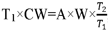
- the functional area has an even thickness which satisfies 0.1 ⁇ T 2 T 1 ⁇ 0.7 , where T 1 is the thickness of the functional area, and T 2 is the minimum thickness of the extension area.
- the thickness of the functional area ranges from 50 ⁇ m to 150 ⁇ m.
- the minimum thickness of the extension area ranges from 10 ⁇ m to 70 ⁇ m.
- T 1 is the thickness of the functional area, measured in ⁇ m
- T 2 is the minimum thickness of the extension area, measured in ⁇ m
- W is a thickness of the extension area in a direction from the functional area to the non-coating area, measured in mm
- CW is a surface density of the functional area, measured in mg/1540.25 mm 2
- A is a random number greater than or equal to 10 and less than or equal to 35
- B is a random number greater than or equal to 20 and less than or equal to 60.
- an electrochemical apparatus including the foregoing electrode plate.
- an electronic apparatus including the foregoing electrochemical apparatus.
- the present invention when the electrode plate experiences external pressure, no excessive pressure is present in the extension area (the transition area of the functional area in proximity of the non-coating area), so that concentrated stress on the transition area can be relieved, avoiding deformation of the current collector and guaranteeing mechanical properties of the current collector and a current conduction effect in the electrochemical apparatus, thereby improving properties such as cycling performance, safety, and service life of the electrochemical apparatus.
- the present invention does not affect efficiency of the cold pressing manufacturing process of the electrode plate, which is of great significance for actual industrial application.
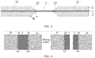
- the electrode plate of the present invention includes a current collector 1, where a functional coating 2 and a non-coating area 3 are provided on at least one surface of the current collector 1, the functional coating 2 includes a functional area 21 and an extension area 22 that extends from the functional area 21 to the non-coating area 3, and the extension area 22 has a minimum thickness (that is, thickness of the extension area 22 at a thinnest position) greater than 0 and a maximum thickness (that is, thickness of the extension area 22 at a thickest position) less than a thickness of the functional area 21.
- the thickness of the extension area 22 is a perpendicular distance from a point on a surface of the extension area 22 to the current collector 1.
- a cross section of the extension area 22 in a thickness direction may be measured with a microscope, to determine thicknesses of the extension area 22 at different positions, for example, the maximum thickness, the minimum thickness, and following thicknesses at a 1/2 width position, 1/3 width position, and 2/3 width position.
- the implementation is not limited thereto.
- the thickness may alternatively be measured by using other conventional methods.
- the non-coating area 3 is a naked foil area without a coating.
- an interface thickness of the functional coating (a sum of the thickness of the functional area 21 and the thickness of the current collector 1) may be 5 times to 20 times the thickness of the non-coating area 3 (that is, thickness of the current collector), without being limited thereto.
- the non-coating area 3 may be a naked foil area reserved for welding a tab, or may be another area without a coating designed as required.
- the non-coating area 3 includes at least one of a naked foil area that is located on a side of the functional coating 2 (as shown in FIG.
- the left side is a schematic structural diagram of a base material including two electrode plates; and the right side is a schematic structural diagram of the two electrode plates obtained by slitting the base material), and a groove that is provided in the functional coating 2 and that exposes a surface of the current collector (with a groove structure shown in FIG. 1 and FIG. 2 ), where a bottom face of the groove is the current collector, and at least two side faces of the groove are the functional coating.
- a cross section of the non-coating area is, for example, rectangular/square (as shown in FIG. 6 ), or round, or in other shapes.
- a quantity of the non-coating area 3 may be one or more, which may be set as required in a specific implementation.
- the thickness of the extension area 22 is substantially unchanged or decreasing in an extension direction toward the non-coating area 3, which helps to resolve the problem of concentrated stress in a transition area between the functional coating and the non-coating area, improve strength of the current collector, and further guarantee functioning of the electrode plate.
- a thickness of the extension area 22 at a position closest to the non-coating area 3 is the minimum thickness of the extension area 22, and a thickness thereof at a position farthest away from the non-coating area 2 is the maximum thickness of the extension area 22.
- the minimum thickness of the extension area 22 is greater than 0, meaning that the extension area 22 has a side face parallel to a thickness direction of the functional coating, on a side in proximity of the non-coating area 3.
- the surface of the extension area 22 is a flat surface, meaning the thickness of the extension area 22 is unchanged in the extension direction toward the non-coating area 3, and the non-coating area 3 has an even thickness (a minimum thickness and a maximum thickness of the non-coating area 3 are substantially equal, which is defined as a thickness difference within a range of 1 ⁇ m); or as shown in FIG. 4 , the surface of the extension area 22 is an inclined surface, meaning the thickness of the extension area 22 is gradually decreasing in the direction toward the non-coating area 3, with a decreasing rate unchanged; or as shown in FIG.
- the surface of the extension area 22 is a cambered surface, which may be specifically a cambered concave surface (the cambered surface is a concave one), meaning the thickness of the extension area 22 is gradually decreasing in the direction toward the non-coating area 3, with a decreasing rate gradually reduced in the direction toward the non-coating area 3, or may be a cambered convex surface (the cambered surface is a convex one), meaning the thickness of the extension area 22 is gradually decreasing in the direction toward the non-coating area 3, with a decreasing rate gradually increased in the direction toward the non-coating area 3.
- the accompanying drawings merely show an electrode plate structure with a cambered surface that is concave, and an electrode plate structure with a cambered surface that is convex is not shown in the accompanying drawings.
- a thickness of the extension area 22 at a 1/2 width position is less than a thickness at a joint of the extension area 22 and the functional area 21.
- a thickness of the extension area 22 at a 2/3 width position is less than a thickness at a 1/3 width position of the extension area 22.
- the functional area has an even thickness which satisfies 0.1 ⁇ T 2 T 1 ⁇ 0.7 , where T 1 is the thickness of the functional area 21, T 2 is the minimum thickness of the extension area 22, and T 2 T 1 is, for example, 0.1, 0.2, 0.3, 0.4, 0.5, 0.6, 0.7, or a range defined by any two of these numbers, which helps to further relieve the problem of concentrated stress in the transition area and improve properties such as energy density of the electrode plate.
- the functional area 21 has an even thickness.
- the even thickness means that a minimum thickness and a maximum thickness of the functional area 21 are substantially equal, which is defined as a thickness difference within 3 ⁇ m, for example, within 2 ⁇ m, 1 ⁇ m, or a smaller range.
- the thickness T 1 of the functional area 21 may range from 50 ⁇ m to 150 ⁇ m, for example, being 50 ⁇ m, 60 ⁇ m, 70 ⁇ m, 80 ⁇ m, 90 ⁇ m, 100 ⁇ m, 110 ⁇ m, 120 ⁇ m, 130 ⁇ m, 140 ⁇ m, 150 ⁇ m, or in a range defined by any two of these numbers
- the minimum thickness T 2 of the extension area 22 may range from 10 ⁇ m to 70 ⁇ m, for example, being 10 ⁇ m, 20 ⁇ m, 30 ⁇ m, 40 ⁇ m, 50 ⁇ m, 60 ⁇ m, 70 ⁇ m, or in a range defined by any two of these numbers.
- a width W of the extension area 22 ranges from 0.1 mm to 3 mm in the direction from the functional area 21 to the non-coating area 3, for example, being 0.1 mm, 0.5 mm, 1 mm, 1.5 mm, 2 mm, 2.5 mm, 3 mm, or in a range defined by any two of these numbers, which helps to relieve the problem of concentrated stress in the transition area and improve properties such as energy density of the electrode plate.
- a smaller W is more favorable for manufacturing the electrode plate and allows for higher machining efficiency.
- the foregoing electrode plate may be a positive electrode plate or a negative electrode plate.
- T 1 is the thickness of the functional area, measured in ⁇ m
- T 2 is the minimum thickness of the extension area, measured in ⁇ m
- W is a thickness of the extension area in a direction from the functional area to the non-coating area, measured in mm
- CW is a surface density of the functional area, measured in mg/1540.25 mm 2
- A is a random number greater than or equal to 10 and less than or equal to 35
- B is a random number greater than or equal to 20 and less than or equal to 60.
- the present invention may use a conventional current collector in the art.
- the current collector when the foregoing electrode plate is a positive electrode plate, the current collector may be aluminum foil; and when the foregoing electrode plate is a negative electrode plate, the current collector may be copper foil, or the like.
- the functional coating 2 and the non-coating area 3 may be provided on only one surface of the current collector 1, or the functional coating 2 and the non-coating area 3 may be provided on both front and back surfaces of the current collector 1. Comparatively, the latter case better improves properties such as energy density of the electrode plate.
- the two cases may be selected as required.
- two surfaces of the current collector 1 each include a functional coating 2 and a non-coating area 3, where the functional coatings 2 on the two surfaces of the current collector 1 are corresponding in position, and the non-coating areas 3 on the two surfaces of the current collector 1 are corresponding in position.
- a direct projection of the functional coating 2 on one surface of the current collector 1 parallel to a surface of the electrode plate coincides with a positive projection of the functional coating 2 on the other surface of the current collector 1 parallel to the surface of the electrode plate
- a direct projection of the non-coating area 3 on one surface of the current collector 1 parallel to the surface of the current collector 1 coincides with a direct projection of the non-coating area 3 on the other surface of the current collector 1 parallel to the surface of the current collector (as shown in FIG. 3 to FIG. 5 ), where the functional areas on the two front and back surfaces of the current collector are corresponding in position, and extension areas on two front and back surfaces of the current collector are corresponding in position.
- the implementation is not limited thereto.
- the functional coating and the non-coating area may be provided on other positions of the front and back surfaces of the current collector as required, as long as the foregoing extension area is present between the functional area and the non-coating area.
- the functional coating includes, for example, an active substance layer, and may further include, as required, other coatings such as a protection layer fitting with the active substance layer.
- the functional area and the extension area each include an active substance, a conductive agent, and a binder, where a mass percentage of the active substance ranges from 85% to 98%, a mass percentage of the conductive agent ranges from 0.01% to 3%, and a mass percentage of the binder ranges from 0.1% to 5%.
- the functional area and the extension area may have the same or different constituents and the same or different amounts of constituents, and preferably the same in general, to help relieve the problem of concentrated stress in the transition area and simplify a manufacturing process of the electrode plate.
- the conductive agent may include at least one of conductive carbon black (SP), acetylene black, Ketjen black, carbon fiber, and the like.
- the binder may include at least one of polyvinylidene fluoride (PVDF), polyvinyl alcohol, hydroxypropyl cellulose, diacetyl cellulose, polyvinyl chloride, carboxylated polyvinyl chloride, polyvinyl fluoride, ethylidene-containing oxide polymer, polyvinylpyrrolidone, polyurethane, polytetrafluoroethylene, poly(vinylidene fluoride), polyethylene, polypropylene, styrene-butadiene rubber (SBR), acrylic styrene-butadiene rubber, epoxy resin, nylon, and the like.
- PVDF polyvinylidene fluoride
- SBR styrene-butadiene rubber
- the active substance may include at least one of lithium cobalt oxide (LCO), lithium iron phosphate (LFP), lithium manganate, nickel-cobalt-manganese (NCM) ternary material, and nickel-cobalt-aluminum (NCA) ternary material.
- the active substance may include at least one of graphite, mesocarbon microbead (MCMB), hard carbon, soft carbon, silicon, and silicon-carbon compound (or referred to as silicon carbon compound).
- the graphite may specifically include artificial graphite and/or natural graphite.
- the electrode plate of the present invention may be manufactured by a conventional method in the art. For example, a slurry containing a functional coating component may be coated on a surface of a metal foil material (a current collector), followed by drying and rolling, to form a functional coating on the surface of the metal foil material; then, based on a preset position of the non-coating area, a coating on the preset position of the non-coating area is removed by laser cleaning or the like to expose a surface of the current collector and form the non-coating area, meanwhile a part of the functional coating in proximity of the non-coating area is thinned according to parameters such as shape of the extension area, to form the extension area, and then slitting is performed according to parameters such as preset shape and size of the electrode plate, to obtain electrode plates.
- a slurry containing a functional coating component may be coated on a surface of a metal foil material (a current collector), followed by drying and rolling, to form a functional coating on the surface of the metal foil material; then
- An electrochemical apparatus of the present invention includes the foregoing electrode plate.
- the electrochemical apparatus may be any apparatus in which electrochemical reaction takes place, and may be particularly an electrochemical apparatus that includes a positive electrode with a positive electrode active substance which is capable of occluding and releasing metal ions (such as lithium ions), and a negative electrode with a negative electrode active substance which is capable of occluding and releasing metal ions.
- Specific examples of the electrochemical apparatus may be all types of primary batteries, secondary batteries, fuel batteries, solar batteries, or capacitors, and particularly, the electrochemical apparatus may be a lithium-ion secondary battery.
- the foregoing electrode plate may be a positive electrode plate, or may be a negative electrode plate, or may include a positive electrode plate and a negative electrode plate.
- the electrochemical apparatus further includes a negative electrode plate, where the negative electrode plate may be a conventional negative electrode plate in the art such as a graphite-containing negative electrode plate and a silicon-containing negative electrode plate; and when the electrode plate is a negative electrode plate, the electrochemical energy storage apparatus further includes a positive electrode plate, where the positive electrode plate may be a conventional positive electrode plate in the art. This is not specifically limited in the present invention.
- the electrochemical apparatus further includes a separator located between the positive electrode plate and the negative electrode plate, where the separator is configured to separate the positive electrode plate and the negative electrode plate, and may be a conventional separator in the art. This is not specifically limited in the present invention.
- An electronic apparatus of the present invention includes the foregoing electrochemical apparatus which is used as an energy storage apparatus.
- N-methylpyrrolidone 95% by mass of lithium cobalt oxide, 2% by mass of carbon blank, and 3% by mass of polyvinylidene fluoride were added and mixed to prepare a positive electrode slurry; the positive electrode slurry was coated on a surface of an aluminum foil, followed by drying and rolling, to form a positive electrode active substance layer on the surface of the aluminum foil; and a groove for mounting a positive tab and exposing the surface of the aluminum foil was cut into the positive electrode active substance layer by laser cleaning (as shown in FIG. 1 and FIG. 2 ), and a part of the positive electrode active substance layer in proximity of the groove was thinned to form an extension area (as shown in FIG. 3 to FIG. 5 ), to prepare a positive electrode plate.
- a negative electrode plate structure provided in comparative example 1 is the same as those in examples 1 to 5 except that no extension area is provided between the functional area and the groove.
- a positive electrode plate structure provided in comparative example 2 is the same as those in Examples 6 to 10 except that no extension area is provided between the functional area and the groove.
- Table 1 gives the extension area surface states (flat surface shown in FIG. 3 /inclined surface shown in FIG. 4 /cambered concave surface shown in FIG. 5 ), extension area minimum thicknesses T 2 , extension area widths W, functional area thicknesses T 1 , and measured tensile strengths of electrode plates in examples 1 to 5 and comparative example 1.
- Table 2 gives the extension area surface state (flat surface/inclined surface/cambered concave surface), extension area minimum thicknesses T 2 , extension area widths W, functional area thicknesses T 1 , and measured tensile strengths of electrode plates in examples 6 to 10 and comparative example 2.
- Table 1 Parameters and tensile strengths of negative electrode plates in examples 1 to 5 and comparative example 1 Examples T 1 ( ⁇ m) CW (g/1540.25 mm 2 ) W (mm) T 2 ( ⁇ m) Extension area surface state
- Example 1 100 0.130 1.25 50 See FIG. 3 . 436
- Example 2 100 0.130 1.25 50 See FIG. 4 .
- Example 3 100 0.130 1.25 50 See FIG. 5 . 430 Example 4 100 0.130 3 5 See FIG. 3 . 372 Example 5 100 0.130 3 80 See FIG. 3 . 367 Table 2 Parameters and tensile strengths of positive electrode plates in examples 6 to 10 and comparative example 2 Examples T 1 ( ⁇ m) CW (g/1540.25 mm 2 ) W (mm) T 2 ( ⁇ m) Extension area surface state Tensile strength (MPa) Comparative example 2 88 0.250 1.25 0 / 210 Example 6 88 0.250 1.25 40 See FIG. 3 . 287 Example 7 88 0.250 1.25 40 See FIG. 4 . 271 Example 8 88 0.250 1.25 40 See FIG. 5 . 268 Example 9 88 0.250 3 5 See FIG. 3 . 234 Example 10 88 0.250 3 70 See FIG. 3 . 225
- the tensile strengths of the positive electrode plates in examples 1 to 5 are significantly higher than that of the positive electrode plate in comparative example 1, and the tensile strengths of the negative electrode plates in examples 6 to 10 are significantly higher than that of the negative electrode plate in comparative example 2.
- the strength of the electrode plate is even more improved in examples 1 to 3 and examples 6 to 8. This shows that after the extension area is added, concentrated stress on the electrode plate that is being cold-pressed is greatly reduced, which accordingly reduces deformation of the transition area and allows for excellent tensile strength of the cold-pressed electrode plate.
Landscapes
- Chemical & Material Sciences (AREA)
- Engineering & Computer Science (AREA)
- Chemical Kinetics & Catalysis (AREA)
- Electrochemistry (AREA)
- General Chemical & Material Sciences (AREA)
- Materials Engineering (AREA)
- Manufacturing & Machinery (AREA)
- Power Engineering (AREA)
- Microelectronics & Electronic Packaging (AREA)
- Composite Materials (AREA)
- Battery Electrode And Active Subsutance (AREA)
- Cell Electrode Carriers And Collectors (AREA)
Abstract
Description
- The present invention relates to the field of electrochemical apparatuses, and in particular, to an electrode plate, an electrochemical apparatus, and an electronic apparatus.
- Electrochemical apparatuses such as lithium-ion secondary batteries are widely applied. Scientific and technological development is accompanied by higher requirements for energy density of electrochemical apparatuses. To guarantee or increase the energy density of an electrochemical apparatus, an electrode plate coating generally needs a higher compacted density. Therefore, high pressure needs to be exerted during a cold pressing manufacturing process of an electrode plate. Existing electrode plates are generally manufactured with gap coating. That is, a functional coating and a non-coating area are present on a surface of a current collector then the current collector is slit along the non-coating area to electrode plates. The manufactured electrode plate has a functional coating and a non-coating area. Due to a thickness difference of the functional coating and the non-coating area, when the electrode plate experiences relatively high external pressure (such as the pressure during the cold pressing manufacturing process or other external pressure), concentrated stress caused by the foregoing pressure is present in a part (or a transition area) of the functional coating in proximity of the non-coating area, causing irreversible deformation to the current collector in the transition area, thereby weakening mechanical properties of the current collector and affecting a current conduction effect in the electrochemical apparatus.
- The present invention provides an electrode plate, an electrochemical apparatus, and an electronic apparatus, which resolve the problem that concentrated stress is present in a transition area of an electrode plate coating in proximity of a non-coating area during a cold pressing manufacturing process in the prior art, causing problems such as poor mechanical properties and a poor current conduction effect of a current collector.
- According to one aspect of the present invention, an electrode plate is provided, including a current collector, where a functional coating and a non-coating area are provided on at least one surface of the current collector. The functional coating includes a functional area and an extension area that extends from the functional area to the non-coating area. The extension area has a minimum thickness greater than 0 and a maximum thickness less than a thickness of the functional area.
- According to an embodiment of the present invention, the non-coating area includes at least one of a naked foil area that is located on a side of the functional coating, and a groove that is provided in the functional coating and that exposes a surface of the current collector, where a bottom face of the groove is the current collector, and at least two side faces of the groove are the functional coating.
- According to an embodiment of the present invention, a thickness of the extension area is substantially unchanged or decreasing in an extension direction toward the non-coating area.
- According to an embodiment of the present invention, a width of the extension area ranges from 0.1 mm to 3 mm in a direction from the functional area to the non-coating area.
- According to an embodiment of the present invention, in the direction from the functional area to the non-coating area, a thickness of the extension area at a 1/2 width position is less than a thickness at a joint of the extension area and the functional area.
- According to an embodiment of the present invention, in the direction from the functional area to the non-coating area, a thickness of a 2/3 width position of the extension area is less than a thickness of a 1/3 width position of the extension area.
- According to an embodiment of the present invention, a surface of the extension area is one of a flat surface, an inclined surface, and a cambered surface.
- According to an embodiment of the present invention, the functional area has an even thickness which satisfies

- According to an embodiment of the present invention, the thickness of the functional area ranges from 50 µm to 150 µm.
- According to an embodiment of the present invention, the minimum thickness of the extension area ranges from 10 µm to 70 µm.
- According to an embodiment of the present invention, the electrode plate is a negative electrode plate that satisfies


- According to another aspect of the present invention, an electrochemical apparatus is provided, including the foregoing electrode plate.
- According to still another aspect of the present invention, an electronic apparatus is provided, including the foregoing electrochemical apparatus.
- With the foregoing electrode plate structure design of the present invention, when the electrode plate experiences external pressure, no excessive pressure is present in the extension area (the transition area of the functional area in proximity of the non-coating area), so that concentrated stress on the transition area can be relieved, avoiding deformation of the current collector and guaranteeing mechanical properties of the current collector and a current conduction effect in the electrochemical apparatus, thereby improving properties such as cycling performance, safety, and service life of the electrochemical apparatus. In addition, while guaranteeing the foregoing properties of the electrode plate, the present invention does not affect efficiency of the cold pressing manufacturing process of the electrode plate, which is of great significance for actual industrial application.
-
-
FIG. 1 is a planar view of an electrode plate structure with a functional coating and a groove (with no extension area illustrated); -
FIG. 2 is a sectional view of an electrode plate structure with a functional coating and a groove (with no extension area illustrated); -
FIG. 3 is a sectional view of an electrode plate structure according to an embodiment of the present invention; -
FIG. 4 is a sectional view of an electrode plate structure according to another embodiment of the present invention; -
FIG. 5 is a sectional view of an electrode plate structure according to still another embodiment of the present invention; and -
FIG. 6 is a planar view of an electrode plate structure according to an embodiment of the present invention. - Description of reference signs: 1. current collector; 2. functional coating; 21. functional area; 22. extension area; 3. non-coating area; and W. width of extension area.
- To make persons skilled in the art better understand the solutions of the present invention, the following further describes the present invention in detail with reference to the accompanying drawings.
- As shown in
FIG. 1 to FIG. 6 , the electrode plate of the present invention includes acurrent collector 1, where afunctional coating 2 and anon-coating area 3 are provided on at least one surface of thecurrent collector 1, thefunctional coating 2 includes afunctional area 21 and anextension area 22 that extends from thefunctional area 21 to thenon-coating area 3, and theextension area 22 has a minimum thickness (that is, thickness of theextension area 22 at a thinnest position) greater than 0 and a maximum thickness (that is, thickness of theextension area 22 at a thickest position) less than a thickness of thefunctional area 21. - The thickness of the
extension area 22 is a perpendicular distance from a point on a surface of theextension area 22 to thecurrent collector 1. In a specific implementation, a cross section of theextension area 22 in a thickness direction may be measured with a microscope, to determine thicknesses of theextension area 22 at different positions, for example, the maximum thickness, the minimum thickness, and following thicknesses at a 1/2 width position, 1/3 width position, and 2/3 width position. The implementation, however, is not limited thereto. The thickness may alternatively be measured by using other conventional methods. - The
non-coating area 3 is a naked foil area without a coating. Generally, an interface thickness of the functional coating (a sum of the thickness of thefunctional area 21 and the thickness of the current collector 1) may be 5 times to 20 times the thickness of the non-coating area 3 (that is, thickness of the current collector), without being limited thereto. Specifically, thenon-coating area 3 may be a naked foil area reserved for welding a tab, or may be another area without a coating designed as required. In some embodiments, thenon-coating area 3 includes at least one of a naked foil area that is located on a side of the functional coating 2 (as shown inFIG. 6 , where the left side is a schematic structural diagram of a base material including two electrode plates; and the right side is a schematic structural diagram of the two electrode plates obtained by slitting the base material), and a groove that is provided in thefunctional coating 2 and that exposes a surface of the current collector (with a groove structure shown inFIG. 1 and FIG. 2 ), where a bottom face of the groove is the current collector, and at least two side faces of the groove are the functional coating. A cross section of the non-coating area is, for example, rectangular/square (as shown inFIG. 6 ), or round, or in other shapes. A quantity of thenon-coating area 3 may be one or more, which may be set as required in a specific implementation. - In some embodiments, the thickness of the
extension area 22 is substantially unchanged or decreasing in an extension direction toward thenon-coating area 3, which helps to resolve the problem of concentrated stress in a transition area between the functional coating and the non-coating area, improve strength of the current collector, and further guarantee functioning of the electrode plate. Specifically, a thickness of theextension area 22 at a position closest to thenon-coating area 3 is the minimum thickness of theextension area 22, and a thickness thereof at a position farthest away from thenon-coating area 2 is the maximum thickness of theextension area 22. The minimum thickness of theextension area 22 is greater than 0, meaning that theextension area 22 has a side face parallel to a thickness direction of the functional coating, on a side in proximity of thenon-coating area 3. In some embodiments, that a thickness of theextension area 22 is substantially unchanged in an extension direction toward thenon-coating area 3 means that a thickness difference of theextension area 22 is within a range of 2 µm in the extension direction toward the non-coating area 3 (that is, a difference between the maximum thickness and the minimum thickness of theextension area 22 is within 2 µm, for example, within 1 µm or a smaller range). - For example, as shown in
FIG. 3 , the surface of theextension area 22 is a flat surface, meaning the thickness of theextension area 22 is unchanged in the extension direction toward thenon-coating area 3, and thenon-coating area 3 has an even thickness (a minimum thickness and a maximum thickness of thenon-coating area 3 are substantially equal, which is defined as a thickness difference within a range of 1 µm); or as shown inFIG. 4 , the surface of theextension area 22 is an inclined surface, meaning the thickness of theextension area 22 is gradually decreasing in the direction toward thenon-coating area 3, with a decreasing rate unchanged; or as shown inFIG. 5 , the surface of theextension area 22 is a cambered surface, which may be specifically a cambered concave surface (the cambered surface is a concave one), meaning the thickness of theextension area 22 is gradually decreasing in the direction toward thenon-coating area 3, with a decreasing rate gradually reduced in the direction toward thenon-coating area 3, or may be a cambered convex surface (the cambered surface is a convex one), meaning the thickness of theextension area 22 is gradually decreasing in the direction toward thenon-coating area 3, with a decreasing rate gradually increased in the direction toward thenon-coating area 3. In this embodiment, the accompanying drawings merely show an electrode plate structure with a cambered surface that is concave, and an electrode plate structure with a cambered surface that is convex is not shown in the accompanying drawings. - In some embodiments, in the direction from the
functional area 21 to thenon-coating area 3, a thickness of theextension area 22 at a 1/2 width position is less than a thickness at a joint of theextension area 22 and thefunctional area 21. - In some embodiments, in the direction from the
functional area 21 to thenon-coating area 3, a thickness of theextension area 22 at a 2/3 width position is less than a thickness at a 1/3 width position of theextension area 22. - In some embodiments, the functional area has an even thickness which satisfies

functional area 21, T2 is the minimum thickness of theextension area 22, and
- The
functional area 21 has an even thickness. The even thickness means that a minimum thickness and a maximum thickness of thefunctional area 21 are substantially equal, which is defined as a thickness difference within 3 µm, for example, within 2 µm, 1 µm, or a smaller range. - Specifically, in some embodiments, the thickness T1 of the
functional area 21 may range from 50 µm to 150 µm, for example, being 50 µm, 60 µm, 70 µm, 80 µm, 90 µm, 100 µm, 110 µm, 120 µm, 130 µm, 140 µm, 150 µm, or in a range defined by any two of these numbers, and the minimum thickness T2 of theextension area 22 may range from 10 µm to 70 µm, for example, being 10 µm, 20 µm, 30 µm, 40 µm, 50 µm, 60 µm, 70 µm, or in a range defined by any two of these numbers. - In some embodiments, a width W of the
extension area 22 ranges from 0.1 mm to 3 mm in the direction from thefunctional area 21 to thenon-coating area 3, for example, being 0.1 mm, 0.5 mm, 1 mm, 1.5 mm, 2 mm, 2.5 mm, 3 mm, or in a range defined by any two of these numbers, which helps to relieve the problem of concentrated stress in the transition area and improve properties such as energy density of the electrode plate. Generally, within the foregoing range, a smaller W is more favorable for manufacturing the electrode plate and allows for higher machining efficiency. - In the present invention, the foregoing electrode plate may be a positive electrode plate or a negative electrode plate. In some embodiments, the electrode plate is a negative electrode plate that satisfies


- The present invention may use a conventional current collector in the art. For example, when the foregoing electrode plate is a positive electrode plate, the current collector may be aluminum foil; and when the foregoing electrode plate is a negative electrode plate, the current collector may be copper foil, or the like.
- In the present invention, the
functional coating 2 and thenon-coating area 3 may be provided on only one surface of thecurrent collector 1, or thefunctional coating 2 and thenon-coating area 3 may be provided on both front and back surfaces of thecurrent collector 1. Comparatively, the latter case better improves properties such as energy density of the electrode plate. In a specific implementation, the two cases may be selected as required. For example, in some embodiments, two surfaces of thecurrent collector 1 each include afunctional coating 2 and anon-coating area 3, where thefunctional coatings 2 on the two surfaces of thecurrent collector 1 are corresponding in position, and thenon-coating areas 3 on the two surfaces of thecurrent collector 1 are corresponding in position. That is, a direct projection of thefunctional coating 2 on one surface of thecurrent collector 1 parallel to a surface of the electrode plate coincides with a positive projection of thefunctional coating 2 on the other surface of thecurrent collector 1 parallel to the surface of the electrode plate, and a direct projection of thenon-coating area 3 on one surface of thecurrent collector 1 parallel to the surface of thecurrent collector 1 coincides with a direct projection of thenon-coating area 3 on the other surface of thecurrent collector 1 parallel to the surface of the current collector (as shown inFIG. 3 to FIG. 5 ), where the functional areas on the two front and back surfaces of the current collector are corresponding in position, and extension areas on two front and back surfaces of the current collector are corresponding in position. The implementation, however, is not limited thereto. The functional coating and the non-coating area may be provided on other positions of the front and back surfaces of the current collector as required, as long as the foregoing extension area is present between the functional area and the non-coating area. - In the present invention, the functional coating includes, for example, an active substance layer, and may further include, as required, other coatings such as a protection layer fitting with the active substance layer. In some embodiments, the functional area and the extension area each include an active substance, a conductive agent, and a binder, where a mass percentage of the active substance ranges from 85% to 98%, a mass percentage of the conductive agent ranges from 0.01% to 3%, and a mass percentage of the binder ranges from 0.1% to 5%. The functional area and the extension area may have the same or different constituents and the same or different amounts of constituents, and preferably the same in general, to help relieve the problem of concentrated stress in the transition area and simplify a manufacturing process of the electrode plate.
- In the present invention, for example, the conductive agent may include at least one of conductive carbon black (SP), acetylene black, Ketjen black, carbon fiber, and the like. The binder may include at least one of polyvinylidene fluoride (PVDF), polyvinyl alcohol, hydroxypropyl cellulose, diacetyl cellulose, polyvinyl chloride, carboxylated polyvinyl chloride, polyvinyl fluoride, ethylidene-containing oxide polymer, polyvinylpyrrolidone, polyurethane, polytetrafluoroethylene, poly(vinylidene fluoride), polyethylene, polypropylene, styrene-butadiene rubber (SBR), acrylic styrene-butadiene rubber, epoxy resin, nylon, and the like. When the electrode plate is a positive electrode plate, the active substance may include at least one of lithium cobalt oxide (LCO), lithium iron phosphate (LFP), lithium manganate, nickel-cobalt-manganese (NCM) ternary material, and nickel-cobalt-aluminum (NCA) ternary material. When the electrode plate is a negative electrode plate, the active substance may include at least one of graphite, mesocarbon microbead (MCMB), hard carbon, soft carbon, silicon, and silicon-carbon compound (or referred to as silicon carbon compound). The graphite may specifically include artificial graphite and/or natural graphite.
- The electrode plate of the present invention may be manufactured by a conventional method in the art. For example, a slurry containing a functional coating component may be coated on a surface of a metal foil material (a current collector), followed by drying and rolling, to form a functional coating on the surface of the metal foil material; then, based on a preset position of the non-coating area, a coating on the preset position of the non-coating area is removed by laser cleaning or the like to expose a surface of the current collector and form the non-coating area, meanwhile a part of the functional coating in proximity of the non-coating area is thinned according to parameters such as shape of the extension area, to form the extension area, and then slitting is performed according to parameters such as preset shape and size of the electrode plate, to obtain electrode plates.
- An electrochemical apparatus of the present invention includes the foregoing electrode plate. The electrochemical apparatus may be any apparatus in which electrochemical reaction takes place, and may be particularly an electrochemical apparatus that includes a positive electrode with a positive electrode active substance which is capable of occluding and releasing metal ions (such as lithium ions), and a negative electrode with a negative electrode active substance which is capable of occluding and releasing metal ions. Specific examples of the electrochemical apparatus may be all types of primary batteries, secondary batteries, fuel batteries, solar batteries, or capacitors, and particularly, the electrochemical apparatus may be a lithium-ion secondary battery.
- The foregoing electrode plate may be a positive electrode plate, or may be a negative electrode plate, or may include a positive electrode plate and a negative electrode plate. When the electrode plate is a positive electrode plate, the electrochemical apparatus further includes a negative electrode plate, where the negative electrode plate may be a conventional negative electrode plate in the art such as a graphite-containing negative electrode plate and a silicon-containing negative electrode plate; and when the electrode plate is a negative electrode plate, the electrochemical energy storage apparatus further includes a positive electrode plate, where the positive electrode plate may be a conventional positive electrode plate in the art. This is not specifically limited in the present invention.
- The electrochemical apparatus further includes a separator located between the positive electrode plate and the negative electrode plate, where the separator is configured to separate the positive electrode plate and the negative electrode plate, and may be a conventional separator in the art. This is not specifically limited in the present invention.
- An electronic apparatus of the present invention includes the foregoing electrochemical apparatus which is used as an energy storage apparatus.
- To make the objectives, technical solutions and advantages of the present invention clearer, the following further describes the present invention with reference to the specific examples and comparative examples of the present invention. Apparently, the described examples are some but not all of the examples of the present invention. All other embodiments obtained by a person of ordinary skill in the art based on the examples of the present invention without creative efforts shall fall within the protection scope of the present invention.
- In the following examples and comparative examples, tensile strength of a cold-pressed electrode plate was determined according to the following process: adjusting positions of an upper clamp and a lower clamp, clamping an electrode plate sample with forceps into the clamps, adjusting high-speed train tension software so as to elongate the electrode plate at a stable speed of 20 mm/min, recording a maximum load p at a shear failure, and calculating the tensile strength of the electrode plate according to the equation: tensile strength = p/(width w of electrode plate sample x thickness h of electrode plate sample). The same electrode plate was tested multiple times according to this process, to obtain average tensile strength N of the electrode plate (N is an average found from the multiple tests).
-
- (1) Negative electrode plates provided in the following examples 6 to 10 were manufactured according to the following process.
To deionized water, 96% by mass of graphite, 1% by mass of carbon blank, and 3% by mass of styrene-butadiene rubber were added and mixed to prepare a negative electrode slurry; the negative electrode slurry was coated on a surface of a copper foil, followed by drying and rolling, to form a negative electrode active substance layer on the surface of the copper foil; and a groove for mounting a negative tab and exposing the surface of the copper foil was cut into the negative electrode active substance layer by laser cleaning (as shown inFIG. 1 and FIG. 2 ), and a part of the negative electrode active substance layer in proximity of the groove was thinned to form an extension area (as shown inFIG. 3 to FIG. 5 ), to prepare a negative electrode plate. - (2) Positive electrode plates provided in the following examples 1 to 5 were manufactured according to the following process.
- To N-methylpyrrolidone, 95% by mass of lithium cobalt oxide, 2% by mass of carbon blank, and 3% by mass of polyvinylidene fluoride were added and mixed to prepare a positive electrode slurry; the positive electrode slurry was coated on a surface of an aluminum foil, followed by drying and rolling, to form a positive electrode active substance layer on the surface of the aluminum foil; and a groove for mounting a positive tab and exposing the surface of the aluminum foil was cut into the positive electrode active substance layer by laser cleaning (as shown in
FIG. 1 and FIG. 2 ), and a part of the positive electrode active substance layer in proximity of the groove was thinned to form an extension area (as shown inFIG. 3 to FIG. 5 ), to prepare a positive electrode plate. - A negative electrode plate structure provided in comparative example 1 is the same as those in examples 1 to 5 except that no extension area is provided between the functional area and the groove.
- A positive electrode plate structure provided in comparative example 2 is the same as those in Examples 6 to 10 except that no extension area is provided between the functional area and the groove.
- Table 1 gives the extension area surface states (flat surface shown in
FIG. 3 /inclined surface shown inFIG. 4 /cambered concave surface shown inFIG. 5 ), extension area minimum thicknesses T2, extension area widths W, functional area thicknesses T1, and measured tensile strengths of electrode plates in examples 1 to 5 and comparative example 1. - Table 2 gives the extension area surface state (flat surface/inclined surface/cambered concave surface), extension area minimum thicknesses T2, extension area widths W, functional area thicknesses T1, and measured tensile strengths of electrode plates in examples 6 to 10 and comparative example 2.
Table 1 Parameters and tensile strengths of negative electrode plates in examples 1 to 5 and comparative example 1 Examples T1 (µm) CW (g/1540.25 mm2) W (mm) T2 (µm) Extension area surface state Tensile strength∗ (MPa) Comparative Example 1 100 0.130 1.25 0 / 352 Example 1 100 0.130 1.25 50 See FIG. 3 .436 Example 2 100 0.130 1.25 50 See FIG. 4 .432 Example 3 100 0.130 1.25 50 See FIG. 5 .430 Example 4 100 0.130 3 5 See FIG. 3 .372 Example 5 100 0.130 3 80 See FIG. 3 .367 Table 2 Parameters and tensile strengths of positive electrode plates in examples 6 to 10 and comparative example 2 Examples T1 (µm) CW (g/1540.25 mm2) W (mm) T2 (µm) Extension area surface state Tensile strength (MPa) Comparative example 2 88 0.250 1.25 0 / 210 Example 6 88 0.250 1.25 40 See FIG. 3 .287 Example 7 88 0.250 1.25 40 See FIG. 4 .271 Example 8 88 0.250 1.25 40 See FIG. 5 .268 Example 9 88 0.250 3 5 See FIG. 3 .234 Example 10 88 0.250 3 70 See FIG. 3 .225 - According to the test results, the tensile strengths of the positive electrode plates in examples 1 to 5 are significantly higher than that of the positive electrode plate in comparative example 1, and the tensile strengths of the negative electrode plates in examples 6 to 10 are significantly higher than that of the negative electrode plate in comparative example 2. Particularly, the strength of the electrode plate is even more improved in examples 1 to 3 and examples 6 to 8. This shows that after the extension area is added, concentrated stress on the electrode plate that is being cold-pressed is greatly reduced, which accordingly reduces deformation of the transition area and allows for excellent tensile strength of the cold-pressed electrode plate.
- The foregoing describes examples of specific embodiments and experimental verification of the present invention in detail. It should be understood that a person of ordinary skill in the art can make various modifications and variations based on the concept of the present invention without creative efforts. Any technical solutions that can be obtained by persons skilled in the art through logical analysis, reasoning, or limited experiments based on the concept of the present invention on the basis of the prior art shall fall within the protection scope defined by the claims.
Claims (13)
- An electrode plate, characterized by comprising a current collector, wherein a functional coating and a non-coating area are provided on at least one surface of the current collector, the functional coating comprises a functional area and an extension area that extends from the functional area to the non-coating area, and the extension area has a minimum thickness greater than 0 and a maximum thickness less than a thickness of the functional area.
- The electrode plate according to claim 1, characterized in that the non-coating area comprises at least one of a naked foil area that is located on a side of the functional coating, and a groove that is provided in the functional coating and that exposes a surface of the current collector, wherein a bottom face of the groove is the current collector, and at least two side faces of the groove are the functional coating.
- The electrode plate according to claim 1, characterized in that a thickness of the extension area is substantially unchanged or decreasing in an extension direction toward the non-coating area.
- The electrode plate according to any one of claims 1 to 3, characterized in that a width of the extension area ranges from 0.1 mm to 3 mm in a direction from the functional area to the non-coating area.
- The electrode plate according to claim 4, characterized in that in the direction from the functional area to the non-coating area, a thickness of the extension area at a 1/2 width position is less than a thickness at a joint of the extension area and the functional area.
- The electrode plate according to any one of claims 1 to 3, characterized in that a surface of the extension area is one of a flat surface, an inclined surface, and a cambered surface.
- The electrode plate according to claim 1, characterized in that the functional area has an even thickness which satisfies

- The electrode plate according to claim 4, characterized in that the functional area has an even thickness which satisfies

- The electrode plate according to claim 1 or 7, characterized in that at least one of the following conditions is satisfied:the thickness of the functional area ranges from 50 µm to 150 µm; andthe minimum thickness of the extension area ranges from 10 µm to 70 µm.
- The electrode plate according to claim 1, characterized in thatthe electrode plate is a negative electrode plate that satisfies
 the electrode plate is a positive electrode plate that satisfies
 whereinT1 is the thickness of the functional area, measured in µm;T2 is the minimum thickness of the extension area, measured in µm;W is a thickness of the extension area in a direction from the functional area to the non-coating area, measured in mm;CW is a surface density of the functional area, measured in mg/1540.25 mm2;A is a random number greater than or equal to 10 and less than or equal to 35; andB is a random number greater than or equal to 20 and less than or equal to 60.
 - The electrode plate according to claim 9, characterized in thatthe electrode plate is a negative electrode plate that satisfies
 the electrode plate is a positive electrode plate that satisfies
 whereinT1 is the thickness of the functional area, measured in µm;T2 is the minimum thickness of the extension area, measured in µm;W is a thickness of the extension area in a direction from the functional area to the non-coating area, measured in mm;CW is a surface density of the functional area, measured in mg/1540.25 mm2;A is a random number greater than or equal to 10 and less than or equal to 35; andB is a random number greater than or equal to 20 and less than or equal to 60.
 - An electrochemical apparatus, characterized by comprising the electrode plate according to any one of the claims 1 to 11.
- An electronic apparatus, characterized by comprising the electrochemical apparatus according to claim 12.
Applications Claiming Priority (2)
| Application Number | Priority Date | Filing Date | Title |
|---|---|---|---|
| CN202110320955.5A CN113078284B (en) | 2021-03-25 | 2021-03-25 | Pole piece, electrochemical device and electronic device |
| PCT/CN2022/070377 WO2022199210A1 (en) | 2021-03-25 | 2022-01-05 | Pole piece, electrochemical device, and electronic device |
Publications (2)
| Publication Number | Publication Date |
|---|---|
| EP4089759A1 true EP4089759A1 (en) | 2022-11-16 |
| EP4089759A4 EP4089759A4 (en) | 2023-10-25 |
Family
ID=83363744
Family Applications (1)
| Application Number | Title | Priority Date | Filing Date |
|---|---|---|---|
| EP22710473.4A Pending EP4089759A4 (en) | 2021-03-25 | 2022-01-05 | Pole piece, electrochemical device, and electronic device |
Country Status (2)
| Country | Link |
|---|---|
| US (1) | US20220311012A1 (en) |
| EP (1) | EP4089759A4 (en) |
Family Cites Families (10)
| Publication number | Priority date | Publication date | Assignee | Title |
|---|---|---|---|---|
| JPH1092418A (en) * | 1996-09-19 | 1998-04-10 | Matsushita Electric Ind Co Ltd | Battery electrode plate manufacturing apparatus, manufacturing method and battery electrode plate |
| US7097673B2 (en) * | 2001-06-07 | 2006-08-29 | 3M Innovative Properties Company | Coating edge control |
| JP2005277064A (en) * | 2004-03-24 | 2005-10-06 | Tdk Corp | Electrode and method for manufacturing the same and method for manufacturing electrochemical device and electrochemical device |
| US8926933B2 (en) * | 2004-11-09 | 2015-01-06 | The Board Of Regents Of The University Of Texas System | Fabrication of twisted and non-twisted nanofiber yarns |
| US8092936B2 (en) * | 2007-12-25 | 2012-01-10 | Byd Co. Ltd. | Electrochemical cell having a coiled core |
| CN101662011B (en) * | 2008-08-26 | 2013-05-29 | 比亚迪股份有限公司 | A battery pole piece, its preparation method, and a battery containing the pole piece |
| JP5818150B2 (en) * | 2010-11-05 | 2015-11-18 | 株式会社Gsユアサ | Electrode for power storage element, power storage element using the same, and method for manufacturing electrode for power storage element |
| WO2013187172A1 (en) * | 2012-06-11 | 2013-12-19 | Necエナジーデバイス株式会社 | Electrode manufacturing method |
| CN105742565B (en) * | 2016-02-29 | 2019-03-05 | 宁德新能源科技有限公司 | A kind of lithium ion battery pole piece and preparation method thereof |
| WO2019044526A1 (en) * | 2017-08-29 | 2019-03-07 | 株式会社村田製作所 | Battery, battery pack, electronic equipment, electric-powered vehicle, electric storage device and electric power system |
-
2022
- 2022-01-05 EP EP22710473.4A patent/EP4089759A4/en active Pending
- 2022-03-30 US US17/708,309 patent/US20220311012A1/en active Pending
Also Published As
| Publication number | Publication date |
|---|---|
| EP4089759A4 (en) | 2023-10-25 |
| US20220311012A1 (en) | 2022-09-29 |
Similar Documents
| Publication | Publication Date | Title |
|---|---|---|
| KR102876886B1 (en) | Electrode sheets and batteries | |
| CN113078284B (en) | Pole piece, electrochemical device and electronic device | |
| JP5605443B2 (en) | Non-aqueous solvent bipolar secondary battery current collector and electrode and battery using the same | |
| EP2003715A2 (en) | Current collector for nonaqueous solvent secondary battery, and electrode and battery, which use the current collector | |
| JP4359331B2 (en) | Secondary battery and method for manufacturing secondary battery | |
| US8530084B2 (en) | Electrode structure for non-aqueous electrolyte secondary battery, method for producing the same, and non-aqueous electrolyte secondary battery | |
| DE102016106550B4 (en) | Separator for a nonaqueous electrolyte secondary battery and manufacturing method thereof | |
| JP3403678B2 (en) | Method for producing lithium secondary battery and wound electrode body | |
| CN112820855A (en) | Pole piece and battery | |
| US8883348B2 (en) | Electrode for lithium ion secondary battery | |
| WO2020098788A1 (en) | Positive pole piece and electrochemical apparatus | |
| CN117497699A (en) | A kind of positive electrode sheet and battery | |
| CN117996370B (en) | Manufacturing method of composite current collector pole piece and evaluating method of composite current collector pole piece | |
| CN217062158U (en) | Battery pole piece and battery cell | |
| CN114242941A (en) | Negative plate and application thereof | |
| US11594751B2 (en) | Battery | |
| US20250391856A1 (en) | Positive electrode and preparation method thereof, battery, and energy-storage device | |
| CN114204038B (en) | Current collectors and their applications | |
| KR20230108691A (en) | Electrode, secondary battery, and electrode manufacturing method | |
| EP4089759A1 (en) | Pole piece, electrochemical device, and electronic device | |
| JPH10284059A (en) | Negative electrode plate for lithium ion battery and method for producing the same | |
| JP3168783B2 (en) | Negative electrode plate for non-aqueous electrolyte secondary battery and method for producing the same | |
| CN221125988U (en) | A negative electrode sheet, an electrode assembly and a battery | |
| US20180277825A1 (en) | Method for manufacturing electrode plate and method for manufacturing secondary battery | |
| JP7630605B2 (en) | Steel foil for current collectors, electrodes, and batteries |
Legal Events
| Date | Code | Title | Description |
|---|---|---|---|
| STAA | Information on the status of an ep patent application or granted ep patent |
Free format text: STATUS: UNKNOWN |
|
| STAA | Information on the status of an ep patent application or granted ep patent |
Free format text: STATUS: THE INTERNATIONAL PUBLICATION HAS BEEN MADE |
|
| PUAI | Public reference made under article 153(3) epc to a published international application that has entered the european phase |
Free format text: ORIGINAL CODE: 0009012 |
|
| STAA | Information on the status of an ep patent application or granted ep patent |
Free format text: STATUS: REQUEST FOR EXAMINATION WAS MADE |
|
| 17P | Request for examination filed |
Effective date: 20220325 |
|
| AK | Designated contracting states |
Kind code of ref document: A1 Designated state(s): AL AT BE BG CH CY CZ DE DK EE ES FI FR GB GR HR HU IE IS IT LI LT LU LV MC MK MT NL NO PL PT RO RS SE SI SK SM TR |
|
| A4 | Supplementary search report drawn up and despatched |
Effective date: 20230927 |
|
| RIC1 | Information provided on ipc code assigned before grant |
Ipc: H01G 11/26 20130101ALI20230921BHEP Ipc: H01M 4/583 20100101ALI20230921BHEP Ipc: H01M 4/131 20100101ALI20230921BHEP Ipc: H01G 11/86 20130101ALI20230921BHEP Ipc: H01M 4/02 20060101ALI20230921BHEP Ipc: H01M 10/0525 20100101ALI20230921BHEP Ipc: H01M 4/66 20060101ALI20230921BHEP Ipc: H01M 4/04 20060101ALI20230921BHEP Ipc: H01G 11/70 20130101ALI20230921BHEP Ipc: H01G 11/28 20130101ALI20230921BHEP Ipc: H01M 4/139 20100101ALI20230921BHEP Ipc: H01M 4/13 20100101AFI20230921BHEP |
|
| DAV | Request for validation of the european patent (deleted) | ||
| DAX | Request for extension of the european patent (deleted) |