EP4089725A1 - Semiconductor apparatus, preparation method therefor, and three-dimensional integrated circuit - Google Patents
Semiconductor apparatus, preparation method therefor, and three-dimensional integrated circuit Download PDFInfo
- Publication number
- EP4089725A1 EP4089725A1 EP21847280.1A EP21847280A EP4089725A1 EP 4089725 A1 EP4089725 A1 EP 4089725A1 EP 21847280 A EP21847280 A EP 21847280A EP 4089725 A1 EP4089725 A1 EP 4089725A1
- Authority
- EP
- European Patent Office
- Prior art keywords
- layer
- heat conductive
- base substrate
- tsv structure
- conductive layer
- Prior art date
- Legal status (The legal status is an assumption and is not a legal conclusion. Google has not performed a legal analysis and makes no representation as to the accuracy of the status listed.)
- Pending
Links
Images












Classifications
-
- H—ELECTRICITY
- H10—SEMICONDUCTOR DEVICES; ELECTRIC SOLID-STATE DEVICES NOT OTHERWISE PROVIDED FOR
- H10W—GENERIC PACKAGES, INTERCONNECTIONS, CONNECTORS OR OTHER CONSTRUCTIONAL DETAILS OF DEVICES COVERED BY CLASS H10
- H10W20/00—Interconnections in chips, wafers or substrates
- H10W20/20—Interconnections within wafers or substrates, e.g. through-silicon vias [TSV]
-
- H—ELECTRICITY
- H10—SEMICONDUCTOR DEVICES; ELECTRIC SOLID-STATE DEVICES NOT OTHERWISE PROVIDED FOR
- H10W—GENERIC PACKAGES, INTERCONNECTIONS, CONNECTORS OR OTHER CONSTRUCTIONAL DETAILS OF DEVICES COVERED BY CLASS H10
- H10W40/00—Arrangements for thermal protection or thermal control
- H10W40/20—Arrangements for cooling
- H10W40/22—Arrangements for cooling characterised by their shape, e.g. having conical or cylindrical projections
-
- H—ELECTRICITY
- H10—SEMICONDUCTOR DEVICES; ELECTRIC SOLID-STATE DEVICES NOT OTHERWISE PROVIDED FOR
- H10W—GENERIC PACKAGES, INTERCONNECTIONS, CONNECTORS OR OTHER CONSTRUCTIONAL DETAILS OF DEVICES COVERED BY CLASS H10
- H10W20/00—Interconnections in chips, wafers or substrates
- H10W20/01—Manufacture or treatment
- H10W20/021—Manufacture or treatment of interconnections within wafers or substrates
- H10W20/023—Manufacture or treatment of interconnections within wafers or substrates the interconnections being through-semiconductor vias
-
- H—ELECTRICITY
- H10—SEMICONDUCTOR DEVICES; ELECTRIC SOLID-STATE DEVICES NOT OTHERWISE PROVIDED FOR
- H10W—GENERIC PACKAGES, INTERCONNECTIONS, CONNECTORS OR OTHER CONSTRUCTIONAL DETAILS OF DEVICES COVERED BY CLASS H10
- H10W20/00—Interconnections in chips, wafers or substrates
- H10W20/01—Manufacture or treatment
- H10W20/021—Manufacture or treatment of interconnections within wafers or substrates
- H10W20/023—Manufacture or treatment of interconnections within wafers or substrates the interconnections being through-semiconductor vias
- H10W20/0249—Manufacture or treatment of interconnections within wafers or substrates the interconnections being through-semiconductor vias wherein the through-semiconductor via protrudes from backsides of the chips, wafers or substrates during the manufacture
-
- H—ELECTRICITY
- H10—SEMICONDUCTOR DEVICES; ELECTRIC SOLID-STATE DEVICES NOT OTHERWISE PROVIDED FOR
- H10W—GENERIC PACKAGES, INTERCONNECTIONS, CONNECTORS OR OTHER CONSTRUCTIONAL DETAILS OF DEVICES COVERED BY CLASS H10
- H10W20/00—Interconnections in chips, wafers or substrates
- H10W20/01—Manufacture or treatment
- H10W20/031—Manufacture or treatment of conductive parts of the interconnections
- H10W20/056—Manufacture or treatment of conductive parts of the interconnections by filling conductive material into holes, grooves or trenches
-
- H—ELECTRICITY
- H10—SEMICONDUCTOR DEVICES; ELECTRIC SOLID-STATE DEVICES NOT OTHERWISE PROVIDED FOR
- H10W—GENERIC PACKAGES, INTERCONNECTIONS, CONNECTORS OR OTHER CONSTRUCTIONAL DETAILS OF DEVICES COVERED BY CLASS H10
- H10W40/00—Arrangements for thermal protection or thermal control
- H10W40/20—Arrangements for cooling
- H10W40/22—Arrangements for cooling characterised by their shape, e.g. having conical or cylindrical projections
- H10W40/226—Arrangements for cooling characterised by their shape, e.g. having conical or cylindrical projections characterised by projecting parts, e.g. fins to increase surface area
- H10W40/228—Arrangements for cooling characterised by their shape, e.g. having conical or cylindrical projections characterised by projecting parts, e.g. fins to increase surface area the projecting parts being wire-shaped or pin-shaped
-
- H—ELECTRICITY
- H10—SEMICONDUCTOR DEVICES; ELECTRIC SOLID-STATE DEVICES NOT OTHERWISE PROVIDED FOR
- H10W—GENERIC PACKAGES, INTERCONNECTIONS, CONNECTORS OR OTHER CONSTRUCTIONAL DETAILS OF DEVICES COVERED BY CLASS H10
- H10W40/00—Arrangements for thermal protection or thermal control
- H10W40/20—Arrangements for cooling
- H10W40/25—Arrangements for cooling characterised by their materials
- H10W40/255—Arrangements for cooling characterised by their materials having a laminate or multilayered structure, e.g. direct bond copper [DBC] ceramic substrates
-
- H—ELECTRICITY
- H10—SEMICONDUCTOR DEVICES; ELECTRIC SOLID-STATE DEVICES NOT OTHERWISE PROVIDED FOR
- H10W—GENERIC PACKAGES, INTERCONNECTIONS, CONNECTORS OR OTHER CONSTRUCTIONAL DETAILS OF DEVICES COVERED BY CLASS H10
- H10W70/00—Package substrates; Interposers; Redistribution layers [RDL]
- H10W70/01—Manufacture or treatment
- H10W70/05—Manufacture or treatment of insulating or insulated package substrates, or of interposers, or of redistribution layers
-
- H—ELECTRICITY
- H10—SEMICONDUCTOR DEVICES; ELECTRIC SOLID-STATE DEVICES NOT OTHERWISE PROVIDED FOR
- H10W—GENERIC PACKAGES, INTERCONNECTIONS, CONNECTORS OR OTHER CONSTRUCTIONAL DETAILS OF DEVICES COVERED BY CLASS H10
- H10W70/00—Package substrates; Interposers; Redistribution layers [RDL]
- H10W70/01—Manufacture or treatment
- H10W70/05—Manufacture or treatment of insulating or insulated package substrates, or of interposers, or of redistribution layers
- H10W70/095—Manufacture or treatment of insulating or insulated package substrates, or of interposers, or of redistribution layers of vias therein
-
- H—ELECTRICITY
- H10—SEMICONDUCTOR DEVICES; ELECTRIC SOLID-STATE DEVICES NOT OTHERWISE PROVIDED FOR
- H10W—GENERIC PACKAGES, INTERCONNECTIONS, CONNECTORS OR OTHER CONSTRUCTIONAL DETAILS OF DEVICES COVERED BY CLASS H10
- H10W70/00—Package substrates; Interposers; Redistribution layers [RDL]
- H10W70/60—Insulating or insulated package substrates; Interposers; Redistribution layers
- H10W70/62—Insulating or insulated package substrates; Interposers; Redistribution layers characterised by their interconnections
- H10W70/63—Vias, e.g. via plugs
- H10W70/635—Through-vias
-
- H—ELECTRICITY
- H10—SEMICONDUCTOR DEVICES; ELECTRIC SOLID-STATE DEVICES NOT OTHERWISE PROVIDED FOR
- H10W—GENERIC PACKAGES, INTERCONNECTIONS, CONNECTORS OR OTHER CONSTRUCTIONAL DETAILS OF DEVICES COVERED BY CLASS H10
- H10W70/00—Package substrates; Interposers; Redistribution layers [RDL]
- H10W70/60—Insulating or insulated package substrates; Interposers; Redistribution layers
- H10W70/62—Insulating or insulated package substrates; Interposers; Redistribution layers characterised by their interconnections
- H10W70/65—Shapes or dispositions of interconnections
-
- H—ELECTRICITY
- H10—SEMICONDUCTOR DEVICES; ELECTRIC SOLID-STATE DEVICES NOT OTHERWISE PROVIDED FOR
- H10W—GENERIC PACKAGES, INTERCONNECTIONS, CONNECTORS OR OTHER CONSTRUCTIONAL DETAILS OF DEVICES COVERED BY CLASS H10
- H10W20/00—Interconnections in chips, wafers or substrates
- H10W20/01—Manufacture or treatment
- H10W20/031—Manufacture or treatment of conductive parts of the interconnections
- H10W20/032—Manufacture or treatment of conductive parts of the interconnections of conductive barrier, adhesion or liner layers
- H10W20/042—Manufacture or treatment of conductive parts of the interconnections of conductive barrier, adhesion or liner layers the barrier, adhesion or liner layers being seed or nucleation layers
-
- H—ELECTRICITY
- H10—SEMICONDUCTOR DEVICES; ELECTRIC SOLID-STATE DEVICES NOT OTHERWISE PROVIDED FOR
- H10W—GENERIC PACKAGES, INTERCONNECTIONS, CONNECTORS OR OTHER CONSTRUCTIONAL DETAILS OF DEVICES COVERED BY CLASS H10
- H10W20/00—Interconnections in chips, wafers or substrates
- H10W20/01—Manufacture or treatment
- H10W20/071—Manufacture or treatment of dielectric parts thereof
- H10W20/074—Manufacture or treatment of dielectric parts thereof of dielectric parts comprising thin functional dielectric layers, e.g. dielectric etch-stop, barrier, capping or liner layers
- H10W20/076—Manufacture or treatment of dielectric parts thereof of dielectric parts comprising thin functional dielectric layers, e.g. dielectric etch-stop, barrier, capping or liner layers in via holes or trenches
-
- H—ELECTRICITY
- H10—SEMICONDUCTOR DEVICES; ELECTRIC SOLID-STATE DEVICES NOT OTHERWISE PROVIDED FOR
- H10W—GENERIC PACKAGES, INTERCONNECTIONS, CONNECTORS OR OTHER CONSTRUCTIONAL DETAILS OF DEVICES COVERED BY CLASS H10
- H10W70/00—Package substrates; Interposers; Redistribution layers [RDL]
- H10W70/01—Manufacture or treatment
- H10W70/02—Manufacture or treatment of conductive package substrates serving as an interconnection, e.g. of metal plates
Definitions
- This disclosure relates to the technical field of semiconductors, and in particular, to a semiconductor apparatus, a method for manufacturing a semiconductor apparatus, and a three-dimensional integrated circuit including the semiconductor apparatus.
- the three-dimensional integrated circuit can achieve high transmission speeds and chip level miniaturization packaging, meeting the light and thin trend of portable electronic products, and thus has attracted more and more attention.
- the heat dissipation effect of the multi-chip packages thereof is relatively poor, the usage range thereof is limited.
- the purpose of this disclosure is to overcome the disadvantages of the prior at and provide a semiconductor apparatus, a method for manufacturing a semiconductor apparatus, and a three-dimensional integrated circuit including the semiconductor apparatus.
- a semiconductor apparatus including:
- a method for manufacturing a semiconductor apparatus may include:
- a groove is disposed on the substrate; and a first end of the TSV structure is exposed in the groove, and a distance between an end surface of the first end and a bottom wall of the groove is smaller than the depth of the groove.
- the first end of the TSV structure is exposed so as to facilitate heat dissipation; on the other hand, the distance between the end surface of the first end and the bottom wall of the groove is smaller than the depth of the groove, i.e., the first end of the TSV structure is sunken in the groove, and other structures will not be affected.
- the coefficient of thermal expansion of the metal itself of the dummy TSV structure 13 is far greater than that of the base substrate 1, if the heat dissipation efficiency of the chip is poor, it can cause the thermal expansion of the dummy TSV structure 13 to apply stress on the base substrate 1, so as to cause deformation of the base substrate 1 and the integrated structure as well as drifting of component characteristics.
- the semiconductor apparatus can include a substrate and a TSV structure 10; the TSV structure 10 is also a dummy TSV structure 13.
- the TSV structure 10 mentioned below is also a dummy TSV structure 13.
- a groove is disposed on the substrate; the TSV structure 10 is disposed on the substrate; and a first end of the TSV structure 10 is exposed in the groove, and a distance between an end surface of the first end and a bottom wall of the groove is smaller than the depth of the groove.
- the substrate can be a base substrate 1 and the material can be silicon.
- a first groove 11 is disposed on the base substrate 1; and a first end of the TSV structure 10 is exposed in the first groove 11,i.e., a distance between an end surface of the first end of the TSV structure 10 and a bottom wall of the first groove 11 is smaller than the depth of the first groove 11, such that the first end is sunken in the base substrate 1.
- the substrate can include a base substrate 1 and a first insulation layer 31.
- the base material 1 can be a silicon substrate.
- a first groove 11 is disposed on the base substrate 1; and a first end of the TSV structure 10 is exposed in the first groove 11,i.e., a distance between an end surface of the first end of the TSV structure 10 and a bottom wall of the first groove 11 is smaller than the depth of the first groove 11, such that the first end is sunken in the base substrate 1.
- the first insulation layer 31 is disposed on the base substrate 1; the first insulation layer 31 is provided with a first blind hole 41 concentric with the first groove 11.
- the distance between the end surface of the first end of the TSV structure 10 and the bottom wall of the first blind hole 41 is smaller than the depth of the first blind hole 41.
- the substrate can include the base substrate 1 and the first insulation layer 31.
- the base material 1 can be a silicon substrate.
- the first end of the TSV structure 10 projects out of the base substrate 1, i.e., the first end of the TSV structure 10 is exposed to the base substrate 1 since it projects out of the base substrate 1.
- the first insulation layer 31 is disposed on the base substrate 1; the first insulation layer 31 is provided with a first blind hole 41; and the first blind hole 41 makes at least a portion of the first end of the TSV structure 10 exposed to the base substrate 1 exposed to the first insulation layer 31.
- the thickness of the first insulation layer 31 in this exemplary implementation is greater than that in FIG.
- the thickness of the first insulation layer 31 is greater than the height of the first end of the TSV structure 10 exposed to the base substrate 1, such that the distance between the end surface of the exposed first end of the TSV structure 10 and the bottom wall of the first blind hole 41 is smaller than the depth of the first blind hole 41.
- the first end of the TSV structure 10 is exposed so as to facilitate heat dissipation; the distance between the end surface of the first end and the bottom wall of the groove is smaller than the depth of the groove, i.e., the first end of the TSV structure 10 is sunken in the groove, and other structures will not be affected.
- the semiconductor apparatus can further include a heat conductive layer group and a heat dissipation layer group; the heat conductive layer group is disposed in the first blind hole 41; the heat conductive layer group is at least in contact with the end surface of the first end of the TSV structure 10; the thickness of the heat conductive layer group decreases with an increase of a distance from the end surface of the first end; and the heat dissipation layer group is connected to the heat conductive layer group and extends towards a side distal from the TSV structure 10.
- the heat conductive layer group can be set as three layers, i.e., the first heat conductive layer 61, the second heat conductive layer 62, and the third heat conductive layer 63.
- the heat dissipation layer group can also be set as three layers, i.e., the first heat dissipation layer 71, the second heat dissipation layer 72, and the third heat dissipation layer 73.
- An insulation layer is disposed between two adjacent heat conductive layers and heat dissipation layers.
- the first heat conductive layer 61 can be set in a cylindrical shape with a bottom; the depth of the first heat conductive layer 61 is the same as the length of the TSV structure 10 exposed to the first insulation layer 31.
- the first heat conductive layer 61 is sleeved on the first end of the TSV structure 10, i.e., the first heat conductive layer 61 is sleeved at the end of the first end of the TSV structure 10 exposed to the first insulation layer 31; the bottom wall of the first heat conductive layer 61 is in contact with the end surface of the first end of the TSV structure 10; the sidewall of the first heat conductive layer 61 is in contact with the side surface of the TSV structure 10.
- the first heat conductive layer 61 completely covers the portion of the TSV structure 10 exposed to the first insulation layer 31.
- the first heat dissipation layer 71 is connected to an edge of a cylinder wall of the first heat conductive layer 61.
- the first heat dissipation layer 71 can be set in a cylindrical shape with a ring, i.e., the first heat dissipation layer 71 can include a first heat dissipation ring and a first heat dissipation cylinder.
- the first heat dissipation ring is located at the bottom wall of the first blind hole 41; an inner ring surface of the first heat dissipation ring is connected to an edge of the cylinder wall of the first heat conductive layer 61; an outer ring surface of the first heat dissipation ring is connected to the first heat dissipation cylinder; the first heat dissipation cylinder is located at a side of the first insulation layer 31 distal from the base substrate 1.
- the first heat dissipation cylinder extends towards a side distal from the TSV structure 10.
- the second insulation layer 32 is disposed at a side of the first heat dissipation layer 71 proximal to the TSV structure 10.
- the second insulation layer 32 does not completely cover the first heat conductive layer 61, and merely covers the end of the first heat conductive layer 61 connected to the first heat dissipation layer 71; certainly, under the condition that the first heat dissipation ring is set to be relatively wide, the second insulation layer 32 can also be completely disconnected to the first heat conductive layer 61.
- the second insulation layer 32 can also be disposed on the side of the first insulation layer 31 outside the first blind hole 41 distal from the base substrate 1.
- a second heat conductive layer 62 is disposed at a side of the first heat conductive layer 61 distal from the TSV structure 10; the second heat conductive layer 62 is also set in a cylindrical shape with a bottom; the depth of the second heat conductive layer 62 is the same as the length of the first heat conductive layer 61 exposed to the second insulation layer 32.
- the second heat conductive layer 62 is sleeved on an end of a portion of the first heat conductive layer 61, i.e., the second heat conductive layer 62 is sleeved at the end of the first heat conductive layer 61 exposed to the second insulation layer 32; the bottom wall of the second heat conductive layer 62 is in contact with the bottom wall of the first heat conductive layer 61; the sidewall of the second heat conductive layer 62 is in contact with the sidewall of the first heat conductive layer 61.
- the second heat conductive layer 62 completely covers the portion of the first heat conductive layer 61 exposed to the second insulation layer 32.
- the second heat dissipation layer 72 is connected to an edge of a cylinder wall of the second heat conductive layer 62.
- the second heat dissipation layer 72 can be disposed as a cylindrical shape, i.e., the cylinder wall of the second heat dissipation layer 72 is connected to a cylinder wall of the second heat conductive layer 62; and the second heat dissipation layer 72 is located at a side of the second insulation layer 32 proximal to the TSV structure 10.
- the second heat dissipation layer 72 extends towards a side distal from the TSV structure 10.
- the third insulation layer 33 is located at a side of the second heat dissipation layer 72 proximal to the TSV structure 10. That is, the third insulation layer 33 does not completely cover the second heat conductive layer 62, and merely covers the end of the second heat conductive layer 62 connected to the second heat dissipation layer 72, such that the bottom wall of the second heat conductive layer 62 is exposed to the third insulation layer 33.
- the first heat dissipation ring is set to be relatively wide, a portion of the sidewall and bottom wall of the second heat conductive layer 62 can also be exposed to the third insulation layer 33.
- the third insulation layer 33 can also be disposed on the side of the second insulation layer 32 outside the first blind hole 41 distal from the base substrate 1.
- a third heat conductive layer 63 is disposed at a side of the second heat conductive layer 62 distal from the TSV structure 10; the third heat conductive layer 63 is set in a sheet shape; the third heat conductive layer 63 is in contact with the bottom wall of the second heat conductive layer 62; the third heat conductive layer 63 completely covers a portion of the third heat conductive layer 62 exposed to the third insulation layer 33.
- the third heat dissipation layer 73 can be set in a cylindrical shape; the third heat dissipation layer 73 is connected to the edge of the third heat conductive layer 63 and is located at a side of the third insulation 33 distal from the base substrate 1; the third heat dissipation layer 73 extends towards a side distal from the TSV structure 10, i.e., the edge of the third heat dissipation layer 73 proximal to the TSV structure 10 is connected to the edge of the third heat conductive layer 63.
- the heat conductive layer group in a multi-layer setting makes the thickness of the heat conductive layer of the end surface of the first end of the TSV structure 10 the thickest. The closer to the end surface of the first end of the TSV structure 10, the thicker the thickness of the heat conductive layer, so as to accelerate the heat energy guide effect, and improve the heat dissipation capability of relatively edge regions of the TSV structure 10.
- the end surface of the first end of the TSV structure 10 is exposed to the first insulation layer 31, i.e., the depth of the first blind hole 41 on the first insulation layer 31 is smaller than the depth of the first blind hone 41 in the exemplary implementations shown in FIG. 6 and FIG. 7 .
- the exemplary implementation shown in FIG. 8 only one heat conductive layer 64 and one heat dissipation layer 74 are disposed, which are respectively the heat conductive layer 64 and the heat dissipation layer 74.
- the heat conductive layer 64 is set in a sheet shape; the heat conductive layer 64 is in contact with the end surface of the first end of the TSV structure 10 exposed to the first insulation layer 31; the heat dissipation layer 74 is connected to the edge of the heat conductive layer 64; the heat dissipation layer 74 is located at a side of the first insulation layer 31 proximal to the TSV structure 10.
- the heat dissipation layer 74 can be set in a cylindrical shape; the heat dissipation layer 74 extends towards a side distal from the TSV structure 10, i.e., the edge of the heat dissipation layer 74 proximal to the TSV structure 10 is connected to the edge of the heat conductive layer 64.
- the materials for the first heat conductive layer 61, the second heat conductive layer 62, the third heat conductive layer 63, the heat conductive layer 64, the first heat dissipation layer 71, the second heat dissipation layer 72, the third heat dissipation layer 73, and the heat dissipation layer 74 can be tungsten, aluminum, copper, gold, silver, or semiconductor metals and combinations thereof, and can also be other non-metal semiconductor materials which own excellent thermal conductivity and combinations thereof; moreover, the materials thereof can be the same or can be different.
- the materials for the first insulation layer 31, the second insulation layer 32, and the third insulation layer 33 can be insulation materials having excellent thermal conductivity or insulation materials mixed with heat conductive metal or metal oxide particles; moreover, the materials thereof can be the same or can be different.
- the structures of the heat conductive layer group and the heat dissipation layer group are not limited to the explanations above, for example, the heat conductive layer group and the heat dissipation layer group can both be set as two layers, and can also be set as four, five, or more layers.
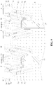
- the semiconductor apparatus can further include four radiation fins 12, each radiation fin 12 is disposed as a cylindrical shape with a bottom having a bottom wall and a sidewall, the bottom wall is connected to an end of the heat dissipation layer group distal from the TSV structure 10, and the sidewall extends towards a side distal from the TSV structure 10.
- the heat dissipation area is increased through the radiation fins 12, so as to enhance the heat dissipation effect.
- the number of the radiation fins 12 can be set according to needs.
- At least one radiation fin 12 is connected between the heat dissipation layer groups of two adjacent TSV structures 10, i.e., one radiation fin 12 is connected to the first heat dissipation layer 71 of one TSV structure 10, and is also connected to the first heat dissipation layer 71 of another adjacent TSV structure 10.
- the heat dissipation layer groups of the two adjacent TSV structures 10 are connected through the radiation fin 12, and the heat dissipation uniformity of the TSV structure 10 is increased.
- the first heat conductive material layer 51 on the first insulation layer 31 outside the first blind hole 41 cannot be removed, such that the first heat conductive layer 61 can also be formed on the first insulation layer 31 outside the first blind hole 41;
- the second heat conductive material layer 52 on the second insulation layer 32 outside the second blind hole 42 cannot be removed, such that the second heat conductive layer 62 can also be formed on the second insulation layer 32 outside the second blind hole 42;
- the third heat conductive material layer on the third insulation layer 33 outside the third blind hole cannot be removed, such that the third heat conductive layer 63 can also be formed on the third insulation layer 33 outside the third blind hole.
- the semiconductor apparatus can further include a dielectric layer 8 and a metal barrier layer 9.
- the dielectric layer 8 is disposed at a side of the heat dissipation layer group distal from the TSV structure 10; and the metal barrier layer 9 is disposed at a side of the dielectric layer 8 distal from the TSV structure 10.
- the dielectric layer 8 and the metal barrier layer 9 prevent the risk of additional leakage and metal contamination.
- the material of the metal barrier layer 9 is Ti, TiN, Ta, TaN, Cu, or a copper alloy.
- this exemplary implementation further provides a three-dimensional integrated circuit.
- the three-dimensional integrated circuit can include the semiconductor apparatus according to any one of the implementations above. The specific structure of the semiconductor apparatus is explained in detail above, and thus is omitted for conciseness.
- the beneficial effects of the three-dimensional integrated circuit provided by the embodiments of this disclosure are the same as the beneficial effects of the semiconductor apparatus provided by the embodiments above, and thus are omitted for conciseness.
- this exemplary implementation further provides a method for manufacturing a semiconductor apparatus. As shown in FIG. 12 , The method for manufacturing a semiconductor apparatus can include the following steps.
- a substrate is provided, and a TSV structure 10 is disposed on the substrate.
- the substrate is patterned to form a groove, such that a first end of the TSV structure 10 is exposed in the groove, and a distance between an end surface of the first end and a bottom wall of the groove is smaller than the depth of the groove.
- a base substrate 1 is provided; a first groove 11 is disposed on the base substrate 1; and a first end of the TSV structure 10 is exposed in the first groove 11, and a distance between an end surface of the first end and a bottom wall of the first groove 11 of the TSV structure 10 is smaller than the depth of the first groove 11.
- a first insulation material layer 21 is formed on the base substrate 1.
- the first insulation material layer 21 fills the first groove 11 on the base substrate 1.
- the first insulation material layer 21 is patterned to form the first insulation layer 31 and the first blind hole 41 concentric with the first groove 11; the first blind hole 41 makes a portion of the first end of the TSV structure 10 exposed to the first insulation layer 31; and the first insulation layer 31 covers a groove wall of the first groove 11 and the base substrate 1.
- the manufacturing method can further include: forming a heat conductive layer group and a heat dissipation layer group, the heat conductive layer group being in the first blind hole 41, the heat conductive layer group being at least in contact with the end surface of the first end of the TSV structure 10, a thickness of the heat conductive layer group decreasing with an increase of a distance from the end surface of the first end, and the heat dissipation layer group being connected to the heat conductive layer group and extending towards a side distal from the TSV structure 10.
- the first heat conductive material layer 51 is formed at the first end of the TSV structure 10 and the first insulation layer 31 through evaporation, sputtering, and other processes. As shown in FIG. 15 , the first heat conductive material layer 51 is patterned to remove the first heat conductive material layer 51 on the first insulation layer 31 outside the first blind hole 41 to form the first heat conductive layer 61 and the first heat dissipation layer 71.
- the first heat conductive layer 61 is formed as a cylindrical shape with a bottom and sleeved at the first end of the TSV structure 10.
- the first heat dissipation layer 71 is formed as a cylindrical shape; the first heat dissipation layer 71 is connected to an edge of a cylinder wall of the first heat conductive layer 61; and the first heat dissipation layer 71 is located at a side of the first insulation layer 31 proximal to the TSV structure 10.
- the specific structures of the first heat conductive layer 61 and the first heat dissipation layer 71 are explained in detail above, and thus are omitted for conciseness.
- the second insulation material layer layer 22 is formed at a side of the first heat conductive layer 61 distal from the base sustrate, a side of the first heat dissipation layer 71 distal from the base substrate, and the side of the first insulation layer 31 distal from the base substrate 1 through the planarization processes.
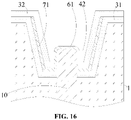
- a second blind hole and a second insulation layer 32 are formed by patterning the second insulation material layer 22; the orthogonal projection of the second blind hole on the base substrate 1 is at least partially overlapped with the orthogonal projection of the first heat conductive layer 61 on the base substrate 1 so as to expose a portion of the first heat conductive layer 61. That is, the second blind hole 42 and the first blind hole 41 are coaxially set; the second insulation layer 32 completely covers the first heat dissipation layer 71 and only covers the end of the first heat conductive layer 61 connected to the first heat dissipation layer 71.
- the second heat conductive material layer 52 is formed at a side of the second insulation layer 32 distal from the substrate and the side of the first heat conductive layer 61 distal from the base substrate 1 through evaporation, sputtering, and other processes.
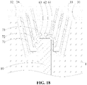
- the second heat conductive material layer 52 is patterned to remove the second heat conductive material layer 52 on the second insulation layer 32 outside the second blind hole 42 to form the second heat conductive layer 62 and the second heat dissipation layer 72;
- the second heat conductive layer 62 is formed as a cylindrical shape with a bottom and is sleeved at a side of a portion of the first heat conductive layer 61 distal from the TSV structure 10, and the second heat dissipation layer 72 is connected to an edge of a cylinder wall of the second heat conductive layer 62 and located at a side of the second insulation layer 32 distal from the base substrate.
- the specific structures of the second heat conductive layer 62 and the second heat dissipation layer 72 are explained in detail above, and thus are omitted for conciseness.
- the third insulation material layer is formed at a side of the second heat conductive layer 62 distal from the base substrate, a side of the second heat dissipation layer 72 distal from the base substrate, and the side of the second insulation layer 32 distal from the base substrate 1 through planarization process, and the third insulation material layer is patterned to form a third blind hole and a third insulation layer 33; and a orthogonal projection of the third blind hole on the base substrate 1 is at least partially overlapped with a orthogonal projection of the second heat conductive layer 62 on the base substrate so as to expose a portion of the second heat conductive layer 62. That is, the third blind hole and the first blind hole 41 are coaxially set; the third insulation layer 33 completely covers the second heat dissipation layer 72 and only covers the end of the second heat conductive layer 62 connected to the second heat dissipation layer 72.
- the third heat conductive material layer is formed at a side of the third insulation layer 33 distal from the substrate and the side of the second heat conductive layer 62 distal from the base substrate 1 through evaporation, sputtering, and other processes; the third heat conductive material layer is patterned to remove the second heat conductive material layer 52 on the third insulation layer 33 outside the third blind hole to form a third heat conductive layer 63 and a third heat dissipation layer 73; the third heat conductive layer 63 is disposed at a side of a portion of the second heat conductive layer 62 distal from the TSV structure 10, and the third heat dissipation layer 73 is connected to an edge of the third heat conductive layer 63 and located at a side of the third insulation layer 33 distal from the substrate.
- the specific structures of the third heat conductive layer 63 and the third heat dissipation layer 73 are explained in detail above, and thus are omitted for conciseness.
- the fourth insulation material layer 24 is formed at a side of the heat dissipation layer group distal from the TSV structure 10 through the planarization process; the fourth insulation material layer 24 completely covers the third heat conductive layer 63 and the third heat dissipation layer 73.
- the fourth insulation material layer 24 is patterned to form the fourth insulation layer 34.
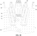
- the etching time is relatively long, such that the second insulation layer 32, the third insulation layer 33, and a portion of the first insulation layer 31 are also etched to form a plurality of fourth blind holes 44; the ends of the first heat dissipation layer 71, the second heat dissipation layer 72, and the third heat dissipation layer 73 distal from the TSV structure 10 are exposed outside the bottom wall of the fourth blind holes 44.
- the fourth heat conductive material layer 54 is formed at a side of the fourth blind hole 44 distal from the TSV structure 10 through evaporation, sputtering, and other processes.
- the fourth heat conductive material layer 54 is patterned to remove the fourth heat conductive material layer 54 outside the fourth blind hole 44 to form a plurality of radiation fins 12; each radiation fin 12 is in a cylindrical shape with a bottom having a bottom wall and a sidewall, the bottom wall is connected to an end of the heat dissipation layer group distal from the TSV structure 10, and the sidewall extending towards a side distal from the TSV structure 10.
- a dielectric layer 8 is formed at a side of the heat dissipation layer group distal from the TSV structure 10; and a metal barrier layer 9 is formed at a side of the dielectric layer 8 distal from the TSV structure 10.
- one radiation fin 12 can also be disposed between two adjacent TSV structures 10, such that the radiation fin 12 is connected between the heat dissipation layer groups of the two adjacent TSV structures 10.
- a surface of the base substrate 1 is a plane; the first end of the TSV structure 10 projects out of the plane to be exposed outside the base substrate 1.
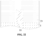
- the first insulation material layer 21 is formed at the first end of the TSV structure 10 on the base substrate 1 through the planarization process. The thickness of the first insulation material layer 21 is greater than the height of the first end of the TSV structure 10 protruding from the base substrate 1; the first insulation material layer 21 completely covers the first end of the TSV structure 10.
- the first insulation material layer 21 is patterned to form the first blind hole 41 and the first insulation layer 31.
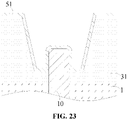
- the first heat conductive material layer 51 is formed on the first insulation layer 31 and the side of the TSV structure 10 distal from the base substrate 1. As shown in FIG. 24 , the first heat conductive material layer 51 is patterned to form the first heat conductive layer 61 and the first heat dissipation layer 71.
- the first heat conductive layer 61 is formed as a cylindrical shape with a bottom and is sleeved at an end of the TSV structure 10.
- the first heat dissipation layer 71 is formed as a cylindrical shape; the first heat dissipation layer 71 is connected to an edge of a cylinder wall of the first heat conductive layer 61; and the first heat dissipation layer 71 is located at a side of the first insulation layer 31 proximal to the TSV structure 10. Then the second heat conductive material layer 22 is formed on the first heat conductive layer 61, the first heat dissipation layer 71, and the side of the first insulation layer 31 distal from the base substrate 1. As shown in FIG.
- a second insulation material layer 22 is patterned to form a second blind hole 42 and a second insulation layer 32; and a orthogonal projection of the second blind hole 42 on the base substrate 1 is at least partially overlapped with a orthogonal projection of the first heat conductive layer 61 on the base substrate 1 so as to expose a portion of the first heat conductive layer 61.
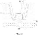
- the second heat conductive material layer 52 is formed on the second insulation layer 32 and the side of the first heat conductive layer 61 distal from the base substrate 1.
- the second heat conductive material layer 52 is patterned to form a second heat conductive layer 62 and a second heat dissipation layer 72;
- the second heat conductive layer 62 is formed as a cylindrical shape with a bottom and is sleeved at a side of a portion of the first heat conductive layer 61 distal from the TSV structure 10;
- the second heat dissipation layer 72 is connected to an edge of a cylinder wall of the second heat conductive layer 62 and is located at a side of the second insulation layer 32 distal from the base substrate 1.
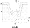
- a third insulation material layer is formed at the second heat conductive layer 62, the second heat dissipation layer 72, and the side of the second insulation layer 32 distal from the base substrate 1 and the third insulation material layer is patterned to form a third blind hole and a third insulation layer 33; a orthogonal projection of the third blind hole on the base substrate 1 is at least partially overlapped with a orthogonal projection of the second heat conductive layer 62 on the base substrate 1 so as to expose a portion of the second heat conductive layer 62.
- the third heat conductive material layer is formed at the third insulation layer 33 and a side of the second heat conductive layer 62 distal from the base substrate 1 and the third heat conductive material layer is patterned to form the third heat conductive layer 63 and the third heat dissipation layer 73; the third heat conductive layer 63 is disposed at a side of the second heat conductive layer 62 distal from the TSV structure 10; the third heat dissipation layer 73 is connected to an edge of the third heat conductive layer 63 and is located at a side of the third insulation layer 33 distal from the base substrate 1.
- the method for manufacturing the semiconductor apparatus having three heat conductive layers and three heat dissipation layers are as above; certainly, one heat conductive layer 64 and one heat dissipation layer 74 can also be set.
- the length of the first end of the TSV structure 10 protruding from the base substrate 1 is shorter than the length of that protruding from the base substrate 1 in the exemplary implementation.
- the first insulation material layer 21 is formed on the base substrate 1 and the first end of the TSV structure 10.
- the first insulation material layer 21 is patterned to form the first blind hole 41 such that the end surface of the first end of the TSV structure 10 exposed to the base substrate 1 is exposed to the first insulation layer 31.
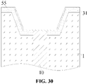
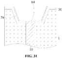
- the heat conductive material layer 55 is formed on the first insulation layer 31 and the end surface of the first end of the TSV structure 10. As shown in FIG. 31 , the heat conductive material layer 55 is patterned to form a heat conductive layer 64 and a heat dissipation layer 74; the heat conductive layer 64 is in contact with the end surface of the first end of the TSV structure 10; and the heat dissipation layer 74 is connected to an edge of the heat conductive layer and is located at a side of the first insulation layer 31 distal from the base substrate 1. As shown in FIG. 32 , the dielectric layer 8 is formed at the first insulation layer 31, the heat conductive layer, and the side of the heat dissipation layer 74 distal from the base substrate 1.
- relativity terms are used in this specification, for example, “up” and “down” are used for describing correspondence of one assembly to another assembly marked in the drawings, these terms used in this specification is merely for convenience, for example, the direction of the example according to the accompanying drawings. As can be understood, if the apparatus marked in the drawings are turned over to be upside down, the assembly at "up” would be the assembly at "down”.
- Other relativity terms for example, “high”, “low”, “top”, “bottom”, and the like are also used for having similar meanings.
- this disclosure does not limit its application to the detailed structure and arranging modes of the parts proposed in this specification.
- This disclosure can have other implementations and can implement and execute in multiple modes.
- the preceding deformation modes and amendment modes fall within the scope of this disclosure.
- this specification discloses and limit all replaceable combinations of two or more separate features which are mentioned or apparent in the text and/or drawings extended by this disclosure. All of these different combinations constitute a plurality of replaceable aspects of this disclosure.
- the implementations of this specification explain the well-known optimal mode for implementing this disclosure and enable a person skilled in the art can use this disclosure.
Landscapes
- Internal Circuitry In Semiconductor Integrated Circuit Devices (AREA)
- Chemical & Material Sciences (AREA)
- Engineering & Computer Science (AREA)
- Ceramic Engineering (AREA)
- Semiconductor Integrated Circuits (AREA)
- Cooling Or The Like Of Semiconductors Or Solid State Devices (AREA)
Abstract
Description
- This application claims priority to
Chinese Patent Application No. 202010699333.3 filed on July 20, 2020 - This disclosure relates to the technical field of semiconductors, and in particular, to a semiconductor apparatus, a method for manufacturing a semiconductor apparatus, and a three-dimensional integrated circuit including the semiconductor apparatus.
- At present, with the development of science and technology, the three-dimensional integrated circuit can achieve high transmission speeds and chip level miniaturization packaging, meeting the light and thin trend of portable electronic products, and thus has attracted more and more attention. However, since the heat dissipation effect of the multi-chip packages thereof is relatively poor, the usage range thereof is limited.
- Hence, it is necessary to research a semiconductor apparatus, a method for manufacturing a semiconductor apparatus, and a three-dimensional integrated circuit including the semiconductor apparatus.
- The information disclosed above by the background art is merely used for enhancing the understanding of the background of this disclosure, and therefore, it may include information of the prior art known by a person having ordinary skill in the art.
- The purpose of this disclosure is to overcome the disadvantages of the prior at and provide a semiconductor apparatus, a method for manufacturing a semiconductor apparatus, and a three-dimensional integrated circuit including the semiconductor apparatus.
- According to an aspect of this disclosure, provided is a semiconductor apparatus, including:
- a substrate, provided with a groove ; and
- a through silicon via (TSV) structure, disposed on the substrate, a first end of the TSV structure being exposed in the groove, and a distance between an end surface of the first end and a bottom wall of the groove being smaller than the depth of the groove.
- In an exemplary embodiment of this disclosure, a method for manufacturing a semiconductor apparatus may include:
- providing a substrate and patterning the substrate to form a groove, comprising:
- providing a base substrate, the first end of the TSV structure being exposed to the base substrate; and
- forming a first insulation material layer on the base substrate and at the first end of the TSV structure, and patterning the first insulation material layer to form a first insulation layer and a first blind hole, the first blind hole making at least a portion of the first end of the TSV structure exposed to the base substrate exposed to the first insulation layer.
- For the semiconductor apparatus of this disclosure, a groove is disposed on the substrate; and a first end of the TSV structure is exposed in the groove, and a distance between an end surface of the first end and a bottom wall of the groove is smaller than the depth of the groove. On one hand, the first end of the TSV structure is exposed so as to facilitate heat dissipation; on the other hand, the distance between the end surface of the first end and the bottom wall of the groove is smaller than the depth of the groove, i.e., the first end of the TSV structure is sunken in the groove, and other structures will not be affected.
- It should be understood that the above general description and the following detailed description are only exemplary and explanatory, and cannot limit this disclosure.
- The accompanying drawings, which are incorporated herein and constitute a part of the specification, illustrate embodiments consistent with this disclosure and, together with the specification, serve to explain the principles of the embodiments of this disclosure. Apparently, the accompanying drawings in the following description show merely some embodiments of this disclosure, and a person of ordinary skill in the art may obtain other accompanying drawings from these accompanying drawings without creative efforts.
-
FIG. 1 is a structural schematic diagram of a semiconductor apparatus in the related art. -
FIG. 2 is a schematic diagram of stress simulation of a base substrate inFIG. 1 . -
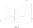
FIG. 3 is a structural schematic diagram of a first exemplary implementation of a semiconductor apparatus of this disclosure. -
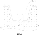
FIG. 4 is a structural schematic diagram of a second exemplary implementation of a semiconductor apparatus of this disclosure. -
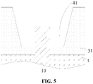
FIG. 5 is a structural schematic diagram of a third exemplary implementation of a semiconductor apparatus of this disclosure. -
FIG. 6 is a structural schematic diagram of a fourth exemplary implementation of a semiconductor apparatus of this disclosure. -
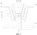
FIG. 7 is a structural schematic diagram of a fifth exemplary implementation of a semiconductor apparatus of this disclosure. -
FIG. 8 is a structural schematic diagram of a sixth exemplary implementation of a semiconductor apparatus of this disclosure. -
FIG. 9 is a structural schematic diagram of a seventh exemplary implementation of a semiconductor apparatus of this disclosure. -
FIG. 10 is a structural schematic diagram of an eighth exemplary implementation of a semiconductor apparatus of this disclosure. -
FIG. 11 is a structural schematic diagram of a ninth exemplary implementation of a semiconductor apparatus of this disclosure. -
FIG. 12 is a flow schematic diagram of an exemplary implementation of a method for manufacturing a semiconductor apparatus of this disclosure. -
FIG. 13 to FIG. 20 are structural schematic diagrams of each step of an exemplary implementation of a method for manufacturing a semiconductor apparatus of this disclosure. -
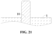
FIG. 21 to FIG. 26 are structural schematic diagrams of each step of another exemplary implementation of a method for manufacturing a semiconductor apparatus of this disclosure. -
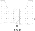
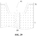
FIG. 27 to FIG. 32 are structural schematic diagrams of each step of a further exemplary implementation of a method for manufacturing a semiconductor apparatus of this disclosure. - Reference numerals of main components in the drawings are explained as follows:
- 1. Base substrate; 11. First groove;
- 21. First insulation material layer; 22. Second insulation material layer; 24. Fourth insulation material layer;
- 31. First insulation layer; 32. Second insulation layer; 33. Third insulation layer; 34. Fourth insulation layer;
- 41. First blind hole; 42. Second blind hole; 44. Fourth blind hole;
- 51. First heat conductive material layer; 52. Second heat conductive material layer; 54. Fourth heat conductive material layer; 55. Heat conductive material layer;
- 61. First heat conductive layer; 62. Second heat conductive layer; 63. Third heat conductive layer; 64. Heat conductive layer;
- 71. First heat dissipation layer; 72. Second heat dissipation layer; 73. Third heat dissipation layer; 74. Heat dissipation layer;
- 8. Dielectric layer; 9. Metal barrier layer; 10. TSV structure; 12. Radiation fin; 13. Dummy TSV structure.
- Exemplary implementations are described more fully now with reference to the accompanying drawings. However, the exemplary implementations can be implemented in multiple forms, an cannot be understood as to be limited to the implementations elaborated herein. On the contrary, providing these implementations enables this disclosure to be comprehensive and complete and the conception of the exemplary implementations are comprehensively delivered to a person skilled in the art. The same reference numerals in the drawings represent the same or similar structures, and thus detailed description thereof would be omitted.
- With reference to the structural schematic diagram of the semiconductor apparatus in the related art as shown in
FIG. 1 , to enhance the heat dissipation effect of the multi-chip packages, some products adopt setting somedummy TSV structures 13 on thebase substrate 1 as assistants, setting the material of thebase substrate 1 to be silicon, and conducting heat through a cylindrical metal of thedummy TSV structures 13. However, the puredummy TSV structures 13 has no prominent heat dissipation effect at the end. With reference to the schematic diagram of stress simulation of a base substrate inFIG. 1 as shown inFIG. 2 , the numbers in the drawings represent stress at each spot in thebase substrate 1. Since the coefficient of thermal expansion of the metal itself of thedummy TSV structure 13 is far greater than that of thebase substrate 1, if the heat dissipation efficiency of the chip is poor, it can cause the thermal expansion of thedummy TSV structure 13 to apply stress on thebase substrate 1, so as to cause deformation of thebase substrate 1 and the integrated structure as well as drifting of component characteristics. - This exemplary implementation first provides a semiconductor apparatus. As shown in
FIG. 3 , the semiconductor apparatus can include a substrate and aTSV structure 10; theTSV structure 10 is also adummy TSV structure 13. TheTSV structure 10 mentioned below is also adummy TSV structure 13. A groove is disposed on the substrate; theTSV structure 10 is disposed on the substrate; and a first end of theTSV structure 10 is exposed in the groove, and a distance between an end surface of the first end and a bottom wall of the groove is smaller than the depth of the groove. - In some exemplary implementations of this disclosure, the substrate can be a
base substrate 1 and the material can be silicon. Afirst groove 11 is disposed on thebase substrate 1; and a first end of theTSV structure 10 is exposed in thefirst groove 11,i.e., a distance between an end surface of the first end of theTSV structure 10 and a bottom wall of thefirst groove 11 is smaller than the depth of thefirst groove 11, such that the first end is sunken in thebase substrate 1. - In some other exemplary implementations of this disclosure, as shown in
FIG. 4 , the substrate can include abase substrate 1 and afirst insulation layer 31. Thebase material 1 can be a silicon substrate. Afirst groove 11 is disposed on thebase substrate 1; and a first end of theTSV structure 10 is exposed in thefirst groove 11,i.e., a distance between an end surface of the first end of theTSV structure 10 and a bottom wall of thefirst groove 11 is smaller than the depth of thefirst groove 11, such that the first end is sunken in thebase substrate 1. Thefirst insulation layer 31 is disposed on thebase substrate 1; thefirst insulation layer 31 is provided with a firstblind hole 41 concentric with thefirst groove 11. The first end of theTSV structure 10 exposed to thebase substrate 1 and protruding out of the bottom wall of the firstblind hole 41, i.e., a portion of the first end of theTSV structure 10 is exposed to thefirst insulation layer 31, such that the bottom of the firstblind hole 41 is formed as a ring shape. The distance between the end surface of the first end of theTSV structure 10 and the bottom wall of the firstblind hole 41 is smaller than the depth of the firstblind hole 41. - In addition, in some other exemplary implementations of this disclosure, as shown in
FIG. 5 , the substrate can include thebase substrate 1 and thefirst insulation layer 31. Thebase material 1 can be a silicon substrate. The first end of theTSV structure 10 projects out of thebase substrate 1, i.e., the first end of theTSV structure 10 is exposed to thebase substrate 1 since it projects out of thebase substrate 1. Thefirst insulation layer 31 is disposed on thebase substrate 1; thefirst insulation layer 31 is provided with a firstblind hole 41; and the firstblind hole 41 makes at least a portion of the first end of theTSV structure 10 exposed to thebase substrate 1 exposed to thefirst insulation layer 31. The thickness of thefirst insulation layer 31 in this exemplary implementation is greater than that inFIG. 4 ; the thickness of thefirst insulation layer 31 is greater than the height of the first end of theTSV structure 10 exposed to thebase substrate 1, such that the distance between the end surface of the exposed first end of theTSV structure 10 and the bottom wall of the firstblind hole 41 is smaller than the depth of the firstblind hole 41. - The first end of the
TSV structure 10 is exposed so as to facilitate heat dissipation; the distance between the end surface of the first end and the bottom wall of the groove is smaller than the depth of the groove, i.e., the first end of theTSV structure 10 is sunken in the groove, and other structures will not be affected. - In some other exemplary implementations, the semiconductor apparatus can further include a heat conductive layer group and a heat dissipation layer group; the heat conductive layer group is disposed in the first
blind hole 41; the heat conductive layer group is at least in contact with the end surface of the first end of theTSV structure 10; the thickness of the heat conductive layer group decreases with an increase of a distance from the end surface of the first end; and the heat dissipation layer group is connected to the heat conductive layer group and extends towards a side distal from theTSV structure 10. - For example, the heat conductive layer group can be set as three layers, i.e., the first
heat conductive layer 61, the secondheat conductive layer 62, and the third heatconductive layer 63. The heat dissipation layer group can also be set as three layers, i.e., the firstheat dissipation layer 71, the secondheat dissipation layer 72, and the thirdheat dissipation layer 73. An insulation layer is disposed between two adjacent heat conductive layers and heat dissipation layers. - As shown in
FIG. 6 andFIG. 7 , specifically, the firstheat conductive layer 61 can be set in a cylindrical shape with a bottom; the depth of the firstheat conductive layer 61 is the same as the length of theTSV structure 10 exposed to thefirst insulation layer 31. The firstheat conductive layer 61 is sleeved on the first end of theTSV structure 10, i.e., the firstheat conductive layer 61 is sleeved at the end of the first end of theTSV structure 10 exposed to thefirst insulation layer 31; the bottom wall of the firstheat conductive layer 61 is in contact with the end surface of the first end of theTSV structure 10; the sidewall of the firstheat conductive layer 61 is in contact with the side surface of theTSV structure 10. The firstheat conductive layer 61 completely covers the portion of theTSV structure 10 exposed to thefirst insulation layer 31. - The first
heat dissipation layer 71 is connected to an edge of a cylinder wall of the firstheat conductive layer 61. The firstheat dissipation layer 71 can be set in a cylindrical shape with a ring, i.e., the firstheat dissipation layer 71 can include a first heat dissipation ring and a first heat dissipation cylinder. The first heat dissipation ring is located at the bottom wall of the firstblind hole 41; an inner ring surface of the first heat dissipation ring is connected to an edge of the cylinder wall of the firstheat conductive layer 61; an outer ring surface of the first heat dissipation ring is connected to the first heat dissipation cylinder; the first heat dissipation cylinder is located at a side of thefirst insulation layer 31 distal from thebase substrate 1. The first heat dissipation cylinder extends towards a side distal from theTSV structure 10. - The
second insulation layer 32 is disposed at a side of the firstheat dissipation layer 71 proximal to theTSV structure 10. Thesecond insulation layer 32 does not completely cover the firstheat conductive layer 61, and merely covers the end of the firstheat conductive layer 61 connected to the firstheat dissipation layer 71; certainly, under the condition that the first heat dissipation ring is set to be relatively wide, thesecond insulation layer 32 can also be completely disconnected to the firstheat conductive layer 61. Thesecond insulation layer 32 can also be disposed on the side of thefirst insulation layer 31 outside the firstblind hole 41 distal from thebase substrate 1. - A second
heat conductive layer 62 is disposed at a side of the firstheat conductive layer 61 distal from theTSV structure 10; the secondheat conductive layer 62 is also set in a cylindrical shape with a bottom; the depth of the secondheat conductive layer 62 is the same as the length of the firstheat conductive layer 61 exposed to thesecond insulation layer 32. The secondheat conductive layer 62 is sleeved on an end of a portion of the firstheat conductive layer 61, i.e., the secondheat conductive layer 62 is sleeved at the end of the firstheat conductive layer 61 exposed to thesecond insulation layer 32; the bottom wall of the secondheat conductive layer 62 is in contact with the bottom wall of the firstheat conductive layer 61; the sidewall of the secondheat conductive layer 62 is in contact with the sidewall of the firstheat conductive layer 61. The secondheat conductive layer 62 completely covers the portion of the firstheat conductive layer 61 exposed to thesecond insulation layer 32. - The second
heat dissipation layer 72 is connected to an edge of a cylinder wall of the secondheat conductive layer 62. The secondheat dissipation layer 72 can be disposed as a cylindrical shape, i.e., the cylinder wall of the secondheat dissipation layer 72 is connected to a cylinder wall of the secondheat conductive layer 62; and the secondheat dissipation layer 72 is located at a side of thesecond insulation layer 32 proximal to theTSV structure 10. The secondheat dissipation layer 72 extends towards a side distal from theTSV structure 10. - The
third insulation layer 33 is located at a side of the secondheat dissipation layer 72 proximal to theTSV structure 10. That is, thethird insulation layer 33 does not completely cover the secondheat conductive layer 62, and merely covers the end of the secondheat conductive layer 62 connected to the secondheat dissipation layer 72, such that the bottom wall of the secondheat conductive layer 62 is exposed to thethird insulation layer 33. Certainly, under the condition that the first heat dissipation ring is set to be relatively wide, a portion of the sidewall and bottom wall of the secondheat conductive layer 62 can also be exposed to thethird insulation layer 33. Thethird insulation layer 33 can also be disposed on the side of thesecond insulation layer 32 outside the firstblind hole 41 distal from thebase substrate 1. - A third heat
conductive layer 63 is disposed at a side of the secondheat conductive layer 62 distal from theTSV structure 10; the third heatconductive layer 63 is set in a sheet shape; the third heatconductive layer 63 is in contact with the bottom wall of the secondheat conductive layer 62; the third heatconductive layer 63 completely covers a portion of the third heatconductive layer 62 exposed to thethird insulation layer 33. - The third
heat dissipation layer 73 can be set in a cylindrical shape; the thirdheat dissipation layer 73 is connected to the edge of the third heatconductive layer 63 and is located at a side of thethird insulation 33 distal from thebase substrate 1; the thirdheat dissipation layer 73 extends towards a side distal from theTSV structure 10, i.e., the edge of the thirdheat dissipation layer 73 proximal to theTSV structure 10 is connected to the edge of the third heatconductive layer 63. - The heat conductive layer group in a multi-layer setting makes the thickness of the heat conductive layer of the end surface of the first end of the
TSV structure 10 the thickest. The closer to the end surface of the first end of theTSV structure 10, the thicker the thickness of the heat conductive layer, so as to accelerate the heat energy guide effect, and improve the heat dissipation capability of relatively edge regions of theTSV structure 10. - In addition, as shown in
FIG. 8 , in this exemplary implementation, the end surface of the first end of theTSV structure 10 is exposed to thefirst insulation layer 31, i.e., the depth of the firstblind hole 41 on thefirst insulation layer 31 is smaller than the depth of the firstblind hone 41 in the exemplary implementations shown inFIG. 6 andFIG. 7 . In the exemplary implementation shown inFIG. 8 , only oneheat conductive layer 64 and oneheat dissipation layer 74 are disposed, which are respectively the heatconductive layer 64 and theheat dissipation layer 74. Specifically, the heatconductive layer 64 is set in a sheet shape; the heatconductive layer 64 is in contact with the end surface of the first end of theTSV structure 10 exposed to thefirst insulation layer 31; theheat dissipation layer 74 is connected to the edge of the heatconductive layer 64; theheat dissipation layer 74 is located at a side of thefirst insulation layer 31 proximal to theTSV structure 10. Theheat dissipation layer 74 can be set in a cylindrical shape; theheat dissipation layer 74 extends towards a side distal from theTSV structure 10, i.e., the edge of theheat dissipation layer 74 proximal to theTSV structure 10 is connected to the edge of the heatconductive layer 64. - The materials for the first
heat conductive layer 61, the secondheat conductive layer 62, the third heatconductive layer 63, the heatconductive layer 64, the firstheat dissipation layer 71, the secondheat dissipation layer 72, the thirdheat dissipation layer 73, and theheat dissipation layer 74 can be tungsten, aluminum, copper, gold, silver, or semiconductor metals and combinations thereof, and can also be other non-metal semiconductor materials which own excellent thermal conductivity and combinations thereof; moreover, the materials thereof can be the same or can be different. - The materials for the
first insulation layer 31, thesecond insulation layer 32, and thethird insulation layer 33 can be insulation materials having excellent thermal conductivity or insulation materials mixed with heat conductive metal or metal oxide particles; moreover, the materials thereof can be the same or can be different. - It is to be explained that the structures of the heat conductive layer group and the heat dissipation layer group are not limited to the explanations above, for example, the heat conductive layer group and the heat dissipation layer group can both be set as two layers, and can also be set as four, five, or more layers.
- As shown in
FIG. 6 continuously, the semiconductor apparatus can further include fourradiation fins 12, eachradiation fin 12 is disposed as a cylindrical shape with a bottom having a bottom wall and a sidewall, the bottom wall is connected to an end of the heat dissipation layer group distal from theTSV structure 10, and the sidewall extends towards a side distal from theTSV structure 10. The heat dissipation area is increased through theradiation fins 12, so as to enhance the heat dissipation effect. Certainly, the number of theradiation fins 12 can be set according to needs. - As shown in
FIG. 9 , at least oneradiation fin 12 is connected between the heat dissipation layer groups of twoadjacent TSV structures 10, i.e., oneradiation fin 12 is connected to the firstheat dissipation layer 71 of oneTSV structure 10, and is also connected to the firstheat dissipation layer 71 of anotheradjacent TSV structure 10. The heat dissipation layer groups of the twoadjacent TSV structures 10 are connected through theradiation fin 12, and the heat dissipation uniformity of theTSV structure 10 is increased. - As shown in
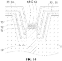
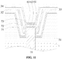
FIG. 10 andFIG. 11 , the first heatconductive material layer 51 on thefirst insulation layer 31 outside the firstblind hole 41 cannot be removed, such that the firstheat conductive layer 61 can also be formed on thefirst insulation layer 31 outside the firstblind hole 41; the second heatconductive material layer 52 on thesecond insulation layer 32 outside the secondblind hole 42 cannot be removed, such that the secondheat conductive layer 62 can also be formed on thesecond insulation layer 32 outside the secondblind hole 42; the third heat conductive material layer on thethird insulation layer 33 outside the third blind hole cannot be removed, such that the third heatconductive layer 63 can also be formed on thethird insulation layer 33 outside the third blind hole. - The semiconductor apparatus can further include a
dielectric layer 8 and ametal barrier layer 9. Thedielectric layer 8 is disposed at a side of the heat dissipation layer group distal from theTSV structure 10; and themetal barrier layer 9 is disposed at a side of thedielectric layer 8 distal from theTSV structure 10. Thedielectric layer 8 and themetal barrier layer 9 prevent the risk of additional leakage and metal contamination. The material of themetal barrier layer 9 is Ti, TiN, Ta, TaN, Cu, or a copper alloy. - Furthermore, this exemplary implementation further provides a three-dimensional integrated circuit. The three-dimensional integrated circuit can include the semiconductor apparatus according to any one of the implementations above. The specific structure of the semiconductor apparatus is explained in detail above, and thus is omitted for conciseness.
- As compared with the prior art, the beneficial effects of the three-dimensional integrated circuit provided by the embodiments of this disclosure are the same as the beneficial effects of the semiconductor apparatus provided by the embodiments above, and thus are omitted for conciseness.
- Furthermore, this exemplary implementation further provides a method for manufacturing a semiconductor apparatus. As shown in
FIG. 12 , The method for manufacturing a semiconductor apparatus can include the following steps. - At step S10, a substrate is provided, and a
TSV structure 10 is disposed on the substrate. - At step S20, the substrate is patterned to form a groove, such that a first end of the
TSV structure 10 is exposed in the groove, and a distance between an end surface of the first end and a bottom wall of the groove is smaller than the depth of the groove. - Each step of The method for manufacturing a semiconductor apparatus is explained in detail below.
- In this exemplary implementation, as shown in
FIG. 3 , abase substrate 1 is provided; afirst groove 11 is disposed on thebase substrate 1; and a first end of theTSV structure 10 is exposed in thefirst groove 11, and a distance between an end surface of the first end and a bottom wall of thefirst groove 11 of theTSV structure 10 is smaller than the depth of thefirst groove 11. - As shown in
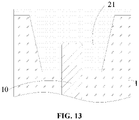
FIG. 13 , a firstinsulation material layer 21 is formed on thebase substrate 1. The firstinsulation material layer 21 fills thefirst groove 11 on thebase substrate 1. As shown inFIG. 4 , the firstinsulation material layer 21 is patterned to form thefirst insulation layer 31 and the firstblind hole 41 concentric with thefirst groove 11; the firstblind hole 41 makes a portion of the first end of theTSV structure 10 exposed to thefirst insulation layer 31; and thefirst insulation layer 31 covers a groove wall of thefirst groove 11 and thebase substrate 1. - In some other exemplary implementations of this disclosure, the manufacturing method can further include: forming a heat conductive layer group and a heat dissipation layer group, the heat conductive layer group being in the first
blind hole 41, the heat conductive layer group being at least in contact with the end surface of the first end of theTSV structure 10, a thickness of the heat conductive layer group decreasing with an increase of a distance from the end surface of the first end, and the heat dissipation layer group being connected to the heat conductive layer group and extending towards a side distal from theTSV structure 10. - Specifically, as shown in
FIG. 14 , the first heatconductive material layer 51 is formed at the first end of theTSV structure 10 and thefirst insulation layer 31 through evaporation, sputtering, and other processes. As shown inFIG. 15 , the first heatconductive material layer 51 is patterned to remove the first heatconductive material layer 51 on thefirst insulation layer 31 outside the firstblind hole 41 to form the firstheat conductive layer 61 and the firstheat dissipation layer 71. The firstheat conductive layer 61 is formed as a cylindrical shape with a bottom and sleeved at the first end of theTSV structure 10. The firstheat dissipation layer 71 is formed as a cylindrical shape; the firstheat dissipation layer 71 is connected to an edge of a cylinder wall of the firstheat conductive layer 61; and the firstheat dissipation layer 71 is located at a side of thefirst insulation layer 31 proximal to theTSV structure 10. The specific structures of the firstheat conductive layer 61 and the firstheat dissipation layer 71 are explained in detail above, and thus are omitted for conciseness. Then the second insulationmaterial layer layer 22 is formed at a side of the firstheat conductive layer 61 distal from the base sustrate, a side of the firstheat dissipation layer 71 distal from the base substrate, and the side of thefirst insulation layer 31 distal from thebase substrate 1 through the planarization processes. - As shown in
FIG. 16 , a second blind hole and asecond insulation layer 32 are formed by patterning the secondinsulation material layer 22; the orthogonal projection of the second blind hole on thebase substrate 1 is at least partially overlapped with the orthogonal projection of the firstheat conductive layer 61 on thebase substrate 1 so as to expose a portion of the firstheat conductive layer 61. That is, the secondblind hole 42 and the firstblind hole 41 are coaxially set; thesecond insulation layer 32 completely covers the firstheat dissipation layer 71 and only covers the end of the firstheat conductive layer 61 connected to the firstheat dissipation layer 71. - As shown in
FIG. 17 , the second heatconductive material layer 52 is formed at a side of thesecond insulation layer 32 distal from the substrate and the side of the firstheat conductive layer 61 distal from thebase substrate 1 through evaporation, sputtering, and other processes. - As shown in
FIG. 18 , the second heatconductive material layer 52 is patterned to remove the second heatconductive material layer 52 on thesecond insulation layer 32 outside the secondblind hole 42 to form the secondheat conductive layer 62 and the secondheat dissipation layer 72; the secondheat conductive layer 62 is formed as a cylindrical shape with a bottom and is sleeved at a side of a portion of the firstheat conductive layer 61 distal from theTSV structure 10, and the secondheat dissipation layer 72 is connected to an edge of a cylinder wall of the secondheat conductive layer 62 and located at a side of thesecond insulation layer 32 distal from the base substrate. The specific structures of the secondheat conductive layer 62 and the secondheat dissipation layer 72 are explained in detail above, and thus are omitted for conciseness. - The third insulation material layer is formed at a side of the second
heat conductive layer 62 distal from the base substrate, a side of the secondheat dissipation layer 72 distal from the base substrate, and the side of thesecond insulation layer 32 distal from thebase substrate 1 through planarization process, and the third insulation material layer is patterned to form a third blind hole and athird insulation layer 33; and a orthogonal projection of the third blind hole on thebase substrate 1 is at least partially overlapped with a orthogonal projection of the secondheat conductive layer 62 on the base substrate so as to expose a portion of the secondheat conductive layer 62. That is, the third blind hole and the firstblind hole 41 are coaxially set; thethird insulation layer 33 completely covers the secondheat dissipation layer 72 and only covers the end of the secondheat conductive layer 62 connected to the secondheat dissipation layer 72. - The third heat conductive material layer is formed at a side of the
third insulation layer 33 distal from the substrate and the side of the secondheat conductive layer 62 distal from thebase substrate 1 through evaporation, sputtering, and other processes; the third heat conductive material layer is patterned to remove the second heatconductive material layer 52 on thethird insulation layer 33 outside the third blind hole to form a third heatconductive layer 63 and a thirdheat dissipation layer 73; the third heatconductive layer 63 is disposed at a side of a portion of the secondheat conductive layer 62 distal from theTSV structure 10, and the thirdheat dissipation layer 73 is connected to an edge of the third heatconductive layer 63 and located at a side of thethird insulation layer 33 distal from the substrate. The specific structures of the third heatconductive layer 63 and the thirdheat dissipation layer 73 are explained in detail above, and thus are omitted for conciseness. - The fourth
insulation material layer 24 is formed at a side of the heat dissipation layer group distal from theTSV structure 10 through the planarization process; the fourthinsulation material layer 24 completely covers the third heatconductive layer 63 and the thirdheat dissipation layer 73. - As shown in
FIG. 19 , the fourthinsulation material layer 24 is patterned to form thefourth insulation layer 34. When patterning the fourthinsulation material layer 24, the etching time is relatively long, such that thesecond insulation layer 32, thethird insulation layer 33, and a portion of thefirst insulation layer 31 are also etched to form a plurality of fourthblind holes 44; the ends of the firstheat dissipation layer 71, the secondheat dissipation layer 72, and the thirdheat dissipation layer 73 distal from theTSV structure 10 are exposed outside the bottom wall of the fourth blind holes 44. - As shown in
FIG. 20 , the fourth heatconductive material layer 54 is formed at a side of the fourthblind hole 44 distal from theTSV structure 10 through evaporation, sputtering, and other processes. As shown inFIG. 6 , the fourth heatconductive material layer 54 is patterned to remove the fourth heatconductive material layer 54 outside the fourthblind hole 44 to form a plurality ofradiation fins 12; eachradiation fin 12 is in a cylindrical shape with a bottom having a bottom wall and a sidewall, the bottom wall is connected to an end of the heat dissipation layer group distal from theTSV structure 10, and the sidewall extending towards a side distal from theTSV structure 10. Adielectric layer 8 is formed at a side of the heat dissipation layer group distal from theTSV structure 10; and ametal barrier layer 9 is formed at a side of thedielectric layer 8 distal from theTSV structure 10. - As shown in
FIG. 9 , oneradiation fin 12 can also be disposed between twoadjacent TSV structures 10, such that theradiation fin 12 is connected between the heat dissipation layer groups of the twoadjacent TSV structures 10. - In addition, it is to be explained that the structure of the substrate is not limited to the explanation above, for example, as shown in
FIG. 21 , a surface of thebase substrate 1 is a plane; the first end of theTSV structure 10 projects out of the plane to be exposed outside thebase substrate 1. As shown inFIG. 22 , the firstinsulation material layer 21 is formed at the first end of theTSV structure 10 on thebase substrate 1 through the planarization process. The thickness of the firstinsulation material layer 21 is greater than the height of the first end of theTSV structure 10 protruding from thebase substrate 1; the firstinsulation material layer 21 completely covers the first end of theTSV structure 10. As shown inFIG. 8 , the firstinsulation material layer 21 is patterned to form the firstblind hole 41 and thefirst insulation layer 31. - The following methods for forming the heat conductive layer group and the heat dissipation layer group can be same as the methods of the exemplary implementations shown in
FIG. 14 to FIG. 18 , and the explanation is made by combining with the accompanying drawings below. - As shown in
FIG. 23 , the first heatconductive material layer 51 is formed on thefirst insulation layer 31 and the side of theTSV structure 10 distal from thebase substrate 1. As shown inFIG. 24 , the first heatconductive material layer 51 is patterned to form the firstheat conductive layer 61 and the firstheat dissipation layer 71. The firstheat conductive layer 61 is formed as a cylindrical shape with a bottom and is sleeved at an end of theTSV structure 10. The firstheat dissipation layer 71 is formed as a cylindrical shape; the firstheat dissipation layer 71 is connected to an edge of a cylinder wall of the firstheat conductive layer 61; and the firstheat dissipation layer 71 is located at a side of thefirst insulation layer 31 proximal to theTSV structure 10. Then the second heatconductive material layer 22 is formed on the firstheat conductive layer 61, the firstheat dissipation layer 71, and the side of thefirst insulation layer 31 distal from thebase substrate 1. As shown inFIG. 25 , a secondinsulation material layer 22 is patterned to form a secondblind hole 42 and asecond insulation layer 32; and a orthogonal projection of the secondblind hole 42 on thebase substrate 1 is at least partially overlapped with a orthogonal projection of the firstheat conductive layer 61 on thebase substrate 1 so as to expose a portion of the firstheat conductive layer 61. As shown inFIG. 26 , the second heatconductive material layer 52 is formed on thesecond insulation layer 32 and the side of the firstheat conductive layer 61 distal from thebase substrate 1. - As shown in
FIG. 7 , the second heatconductive material layer 52 is patterned to form a secondheat conductive layer 62 and a secondheat dissipation layer 72; the secondheat conductive layer 62 is formed as a cylindrical shape with a bottom and is sleeved at a side of a portion of the firstheat conductive layer 61 distal from theTSV structure 10; and the secondheat dissipation layer 72 is connected to an edge of a cylinder wall of the secondheat conductive layer 62 and is located at a side of thesecond insulation layer 32 distal from thebase substrate 1. A third insulation material layer is formed at the secondheat conductive layer 62, the secondheat dissipation layer 72, and the side of thesecond insulation layer 32 distal from thebase substrate 1 and the third insulation material layer is patterned to form a third blind hole and athird insulation layer 33; a orthogonal projection of the third blind hole on thebase substrate 1 is at least partially overlapped with a orthogonal projection of the secondheat conductive layer 62 on thebase substrate 1 so as to expose a portion of the secondheat conductive layer 62. The third heat conductive material layer is formed at thethird insulation layer 33 and a side of the secondheat conductive layer 62 distal from thebase substrate 1 and the third heat conductive material layer is patterned to form the third heatconductive layer 63 and the thirdheat dissipation layer 73; the third heatconductive layer 63 is disposed at a side of the secondheat conductive layer 62 distal from theTSV structure 10; the thirdheat dissipation layer 73 is connected to an edge of the third heatconductive layer 63 and is located at a side of thethird insulation layer 33 distal from thebase substrate 1. - The method for manufacturing the semiconductor apparatus having three heat conductive layers and three heat dissipation layers are as above; certainly, one
heat conductive layer 64 and oneheat dissipation layer 74 can also be set. As shown inFIG. 27 , the length of the first end of theTSV structure 10 protruding from thebase substrate 1 is shorter than the length of that protruding from thebase substrate 1 in the exemplary implementation. As shown inFIG. 28 , the firstinsulation material layer 21 is formed on thebase substrate 1 and the first end of theTSV structure 10. As shown inFIG. 29 , the firstinsulation material layer 21 is patterned to form the firstblind hole 41 such that the end surface of the first end of theTSV structure 10 exposed to thebase substrate 1 is exposed to thefirst insulation layer 31. As shown inFIG. 30 , the heatconductive material layer 55 is formed on thefirst insulation layer 31 and the end surface of the first end of theTSV structure 10. As shown inFIG. 31 , the heatconductive material layer 55 is patterned to form a heatconductive layer 64 and aheat dissipation layer 74; the heatconductive layer 64 is in contact with the end surface of the first end of theTSV structure 10; and theheat dissipation layer 74 is connected to an edge of the heat conductive layer and is located at a side of thefirst insulation layer 31 distal from thebase substrate 1. As shown inFIG. 32 , thedielectric layer 8 is formed at thefirst insulation layer 31, the heat conductive layer, and the side of theheat dissipation layer 74 distal from thebase substrate 1. - The features, structures, or characteristics described above can be combined into one or more implementations in any proper mode; if possible, the features discussed in each embodiment can be exchanged. In the description above, many specific details are provided to provide full understanding of the implementations of this disclosure. However, a person skilled in the art would recognize that the technical solutions of this disclosure can be practiced without one or more of specific details or other methods, assemblies, materials, and the like can be adopted. Under other conditions, well-known structures, materials, or operations are not shown in detail to avoid blurring aspects of this disclosure.
- Although relativity terms are used in this specification, for example, "up" and "down" are used for describing correspondence of one assembly to another assembly marked in the drawings, these terms used in this specification is merely for convenience, for example, the direction of the example according to the accompanying drawings. As can be understood, if the apparatus marked in the drawings are turned over to be upside down, the assembly at "up" would be the assembly at "down". Other relativity terms, for example, "high", "low", "top", "bottom", and the like are also used for having similar meanings. When a certain structure is "on" other structures, it is possible that it refers to a certain structure is integrally formed on other structures, or refers to a certain structure is "directly" disposed on other structure, or refers to a certain structure is "indirectly" disposed on other structures through another structure.
- In this specification, terms "one", "a", "the", "the", and "at least one" are used for representing the existence of one or more elements/constitution parts/and the like; terms "include", "comprise", and "have" are used for representing the open-type meaning of being included and refer to that additional elements/constitution parts/and the like may also exist except the listed elements/constitution parts/and the like; terms "first", "second", "third" and the like are merely sued for marking, rather than limiting the number of objects thereof.
- As can be understood, this disclosure does not limit its application to the detailed structure and arranging modes of the parts proposed in this specification. This disclosure can have other implementations and can implement and execute in multiple modes. The preceding deformation modes and amendment modes fall within the scope of this disclosure. As can be understood, this specification discloses and limit all replaceable combinations of two or more separate features which are mentioned or apparent in the text and/or drawings extended by this disclosure. All of these different combinations constitute a plurality of replaceable aspects of this disclosure. The implementations of this specification explain the well-known optimal mode for implementing this disclosure and enable a person skilled in the art can use this disclosure.
Claims (19)
- A semiconductor apparatus, comprising:a substrate, provided with a groove; anda through silicon via (TSV) structure, disposed on the substrate, a first end of the TSV structure being exposed in the groove, and a distance between an end surface of the first end and a bottom wall of the groove being smaller than a depth of the groove.
- The semiconductor apparatus of claim 1, wherein the substrate comprises:a base substrate, provided with a first groove on the base substrate, the first end being exposed in the first groove; anda first insulation layer, disposed on the base substrate, a first blind hole concentric with the first groove being provided on the first insulation layer, and the first blind hole making at least a portion of the first end of the TSV structure exposed to the base substrate exposed to the first insulation layer.
- The semiconductor apparatus of claim 1, wherein the substrate comprises:a base substrate, the first end of the TSV structure being exposed to the base substrate; anda first insulation layer, disposed on the base substrate, a first blind hole being provided on the first insulation layer, and the first blind hole making at least a portion of the first end of the TSV structure exposed to the base substrate exposed to the first insulation layer.
- The semiconductor apparatus of claim 2 or 3, further comprising:a heat conductive layer group, disposed in the first blind hole, the heat conductive layer group being at least in contact with an end surface of the first end of the TSV structure, and a thickness of the heat conductive layer group decreasing with an increase of a distance from the end surface of the first end; anda heat dissipation layer group, connected to the heat conductive layer group, and extending towards a side distal from the TSV structure.
- The semiconductor apparatus of claim 4, wherein the first end of the TSV structure exposed to the base substrate is exposed to the first insulation layer;the heat conductive layer group comprises:a first heat conductive layer, disposed as a cylindrical shape with a bottom and sleeved at the first end;a second heat conductive layer, disposed as a cylindrical shape with a bottom and sleeved at a side of a portion of the first heat conductive layer distal from the TSV structure; anda third heat conductive layer, disposed at a side of a portion of the second heat conductive layer distal from the TSV structure; andthe heat dissipation layer group comprises:a first heat dissipation layer, connected to an edge of a cylinder wall of the first heat conductive layer and located at a side of the first insulation layer distal from the base substrate;a second insulation layer, located at a side of the first heat dissipation layer proximal to the TSV structure;a second heat dissipation layer, connected to an edge of a cylinder wall of the second heat conductive layer and located at a side of the second insulation layer distal from the base substrate;a third insulation layer, located at a side of the second heat dissipation layer proximal to the TSV structure; anda third heat dissipation layer, connected to an edge of the third heat conductive layer and located at a side of the third insulation layer distal from the base substrate.
- The semiconductor apparatus of claim 4, wherein the end surface of the first end of the TSV structure exposed to the substrate is exposed to the first insulation layer;
the heat conductive layer group comprises:a heat conductive layer in contact with the end surface of the first end of the TSV structure; andthe heat dissipation layer group comprises:
a heat dissipation layer, connected to an edge of the heat conductive layer and located at a side of the first insulation layer proximal to the TSV structure. - The semiconductor apparatus of claim 4, further comprising:
a plurality of radiation fins, each being in a cylindrical shape with a bottom having a bottom wall and a sidewall, the bottom wall being connected to an end of the heat dissipation layer group distal from the TSV structure, and the sidewall extending towards a side distal from the TSV structure. - The semiconductor apparatus of claim 7, wherein at least one of the radiation fins is connected between heat dissipation layer groups of two adjacent TSV structures.
- The semiconductor apparatus of claim 4, further comprising:a dielectric layer, disposed at a side of the heat dissipation layer group distal from the TSV structure; anda metal barrier layer, disposed at a side of the dielectric layer distal from the TSV structure.
- A three-dimensional integrated circuit, comprising:
the semiconductor apparatus according to any one of claims 1-9. - A method for manufacturing a semiconductor apparatus, comprising:providing a substrate, a TSV structure being disposed on the substrate; andpatterning the substrate to form a groove, such that a first end of the TSV structure is exposed in the groove, and a distance between an end surface of the first end and a bottom wall of the groove is smaller than the depth of the groove.
- The method for manufacturing a semiconductor apparatus of claim 11, wherein the operations of providing a substrate and patterning the substrate to form a groove comprises:providing a base substrate, a first groove being provided on the base substrate, and the first end being exposed in the first groove; andforming a first insulation material layer on the base substrate, and patterning the first insulation material layer to form a first insulation layer and a first blind hole concentric with the first groove, the first blind hole making at least a portion of the first end of the TSV structure exposed to the base substrate exposed to the first insulation layer.
- The method for manufacturing a semiconductor apparatus of claim 11, the operations of providing a substrate and patterning the substrate to form a groove, comprising:providing a base substrate, the first end of the TSV structure being exposed to the base substrate; andforming a first insulation material layer on the base substrate and at the first end of the TSV structure, and patterning the first insulation material layer to form a first insulation layer and a first blind hole, the first blind hole making at least a portion of the first end of the TSV structure exposed to the base substrate exposed to the first insulation layer.
- The method for manufacturing a semiconductor apparatus of claim 12 or 13, further comprising:
forming a heat conductive layer group and a heat dissipation layer group, the heat conductive layer group being disposed in the first blind hole, the heat conductive layer group being at least in contact with an end surface of the first end of the TSV structure, a thickness of the heat conductive layer group decreasing with an increase of a distance from the end surface of the first end, and the heat dissipation layer group being connected to the heat conductive layer group and extending towards a side distal from the TSV structure. - The method for manufacturing a semiconductor apparatus of claim 14, wherein the first end of the TSV structure exposed to the base substrate is exposed to the first insulation layer; and the forming a heat conductive layer group and a heat dissipation layer group comprises:forming a first heat conductive material layer at the first end of the TSV structure and a side of the first insulation layer distal from the base substrate and patterning the first heat conductive material layer to form a first heat conductive layer and a first heat dissipation layer, the first heat conductive layer being formed as a cylindrical shape with a bottom and being sleeved at the first end, and the first heat dissipation layer being connected to an edge of a cylinder wall of the first heat conductive layer and located at a side of the first insulation layer distal from the base substrate;forming a second insulation material layer at a side of the first heat conductive layer distal from the base substrate, a side of the first heat dissipation layer distal from the base substrate, and the side of the first insulation layer distal from the base substrate, and patterning the second insulation material layer to form a second blind hole and a second insulation layer, an orthogonal projection of the second blind hole on the base substrate being at least partially overlapped with an orthogonal projection of the first heat conductive layer on the base substrate so as to expose at least a portion of the first heat conductive layer;forming a second heat conductive material layer at a side of the second insulation layer distal from the base substrate and the side of the first heat conductive layer distal from the base substrate, and patterning the second heat conductive material layer to form a second heat conductive layer and a second heat dissipation layer, the second heat conductive layer being formed as a cylindrical shape with a bottom and being sleeved at a side of a portion of the first heat conductive layer distal from the TSV structure, and the second heat dissipation layer being connected to an edge of a cylinder wall of the second heat conductive layer and located at a side of the second insulation layer distal from the base substrate;forming a third insulation material layer at a side of the second heat conductive layer distal from the base substrate, a side of the second heat dissipation layer distal from the base substrate, and the side of the second insulation layer distal from the base substrate, and patterning the third insulation material layer to form a third blind hole and a third insulation layer, an orthogonal projection of the third blind hole on the base substrate being at least partially overlapped with an orthogonal projection of the second heat conductive layer on the base substrate so as to expose at least a portion of the second heat conductive layer; andforming a third heat conductive material layer at a side of the third insulation layer distal from the base substrate and the side of the second heat conductive layer distal from the base substrate, and patterning the third heat conductive material layer to form a third heat conductive layer and a third heat dissipation layer, the third heat conductive layer being disposed at a side of a portion of the second heat conductive layer distal from the TSV structure, and the third heat dissipation layer being connected to an edge of the third heat conductive layer and located at a side of the third insulation layer distal from the base substrate.
- The method for manufacturing a semiconductor apparatus of claim 14, wherein the end surface of the first end of the TSV structure exposed to the base substrate is exposed to the first insulation layer; and the forming a heat conductive layer group and a heat dissipation layer group comprises:
forming a heat conductive material layer at the first insulation layer and the end surface of the first end of the TSV structure and patterning the heat conductive material layer to form a heat conductive layer and a heat dissipation layer, the heat conductive layer being in contact with the end surface of the first end of the TSV structure, and the heat dissipation layer being connected to an edge of the heat conductive layer and located at a side of the first insulation layer distal from the base substrate. - The method for manufacturing a semiconductor apparatus of claim 14, further comprising:forming a fourth insulation material layer at a side of the heat dissipation layer group distal from the TSV structure and patterning the fourth insulation material layer to form a fourth insulation layer and a plurality of fourth blind holes; andforming a fourth heat conductive material layer at a side of the fourth insulation layer distal from the TSV structure and sides of the plurality of fourth blind holes distal from the TSV structure, and patterning the fourth heat conductive material layer to form a plurality of radiation fins, each radiation fin being in a cylindrical shape with a bottom having a bottom wall and a sidewall, the bottom wall being connected to an end of the heat dissipation layer group distal from the TSV structure, and the sidewall extending towards a side distal from the TSV structure.
- The method for manufacturing a semiconductor apparatus of claim 17, wherein at least one of the radiation fins is connected between heat dissipation layer groups of two adjacent TSV structures.
- The method for manufacturing a semiconductor apparatus of claim 14, further comprising:forming a dielectric layer at a side of the heat dissipation layer group distal from the TSV structure; andforming a metal barrier layer at a side of the dielectric layer distal from the TSV structure.
Applications Claiming Priority (2)
| Application Number | Priority Date | Filing Date | Title |
|---|---|---|---|
| CN202010699333.3A CN113964091A (en) | 2020-07-20 | 2020-07-20 | Semiconductor device, manufacturing method thereof and three-dimensional integrated circuit |
| PCT/CN2021/106570 WO2022017255A1 (en) | 2020-07-20 | 2021-07-15 | Semiconductor apparatus, preparation method therefor, and three-dimensional integrated circuit |
Publications (2)
| Publication Number | Publication Date |
|---|---|
| EP4089725A1 true EP4089725A1 (en) | 2022-11-16 |
| EP4089725A4 EP4089725A4 (en) | 2023-08-30 |
Family
ID=79459695
Family Applications (1)
| Application Number | Title | Priority Date | Filing Date |
|---|---|---|---|
| EP21847280.1A Pending EP4089725A4 (en) | 2020-07-20 | 2021-07-15 | Semiconductor apparatus, preparation method therefor, and three-dimensional integrated circuit |
Country Status (6)
| Country | Link |
|---|---|
| US (1) | US12218032B2 (en) |
| EP (1) | EP4089725A4 (en) |
| JP (1) | JP7520141B2 (en) |
| KR (1) | KR102760823B1 (en) |
| CN (1) | CN113964091A (en) |
| WO (1) | WO2022017255A1 (en) |
Cited By (1)
| Publication number | Priority date | Publication date | Assignee | Title |
|---|---|---|---|---|
| US20230352427A1 (en) * | 2021-08-27 | 2023-11-02 | Taiwan Semiconductor Manufacturing Company Limited | Semiconductor die including guard ring structure and three-dimensional device structure including the same |
Families Citing this family (1)
| Publication number | Priority date | Publication date | Assignee | Title |
|---|---|---|---|---|
| CN113675140B (en) * | 2021-08-20 | 2024-05-17 | 武汉新芯集成电路制造有限公司 | Semiconductor device and method for manufacturing the same |
Family Cites Families (15)
| Publication number | Priority date | Publication date | Assignee | Title |
|---|---|---|---|---|
| US7026547B1 (en) | 2005-01-21 | 2006-04-11 | Infineon Technologies Ag | Semiconductor device and a method for fabricating a semiconductor device |
| US8314483B2 (en) | 2009-01-26 | 2012-11-20 | Taiwan Semiconductor Manufacturing Company, Ltd. | On-chip heat spreader |
| US8294261B2 (en) | 2010-01-29 | 2012-10-23 | Texas Instruments Incorporated | Protruding TSV tips for enhanced heat dissipation for IC devices |
| US10181454B2 (en) * | 2010-03-03 | 2019-01-15 | Ati Technologies Ulc | Dummy TSV to improve process uniformity and heat dissipation |
| JP2011249563A (en) * | 2010-05-27 | 2011-12-08 | Panasonic Corp | Semiconductor device and manufacturing method thereof |
| KR101697573B1 (en) | 2010-11-29 | 2017-01-19 | 삼성전자 주식회사 | Semiconductor device, fabricating method thereof, and semiconductor package comprising the semiconductor device |
| US8900994B2 (en) * | 2011-06-09 | 2014-12-02 | Taiwan Semiconductor Manufacturing Company, Ltd. | Method for producing a protective structure |
| KR101870155B1 (en) | 2012-02-02 | 2018-06-25 | 삼성전자주식회사 | Via Connection Structures and Semiconductor Devices Having the Same, and methods of Fabricating the Sames |
| US8772946B2 (en) * | 2012-06-08 | 2014-07-08 | Invensas Corporation | Reduced stress TSV and interposer structures |
| JP6039417B2 (en) | 2012-12-28 | 2016-12-07 | 京セラ株式会社 | Light-emitting element mounting substrate and light-emitting device using the same |
| CN103258789A (en) * | 2013-04-17 | 2013-08-21 | 华中科技大学 | Manufacturing method of through hole interconnection structure and product of through hole interconnection structure |
| CN103426864B (en) * | 2013-08-26 | 2016-08-10 | 华进半导体封装先导技术研发中心有限公司 | TSV structure being applicable to keyset and preparation method thereof |
| US9768147B2 (en) | 2014-02-03 | 2017-09-19 | Micron Technology, Inc. | Thermal pads between stacked semiconductor dies and associated systems and methods |
| US9653381B2 (en) * | 2014-06-17 | 2017-05-16 | Micron Technology, Inc. | Semiconductor structures and die assemblies including conductive vias and thermally conductive elements and methods of forming such structures |
| CN105244311B (en) * | 2014-07-08 | 2018-09-21 | 中芯国际集成电路制造(上海)有限公司 | A kind of semiconductor devices and its manufacturing method, electronic device |
-
2020
- 2020-07-20 CN CN202010699333.3A patent/CN113964091A/en active Pending
-
2021
- 2021-07-15 JP JP2022562361A patent/JP7520141B2/en active Active
- 2021-07-15 WO PCT/CN2021/106570 patent/WO2022017255A1/en not_active Ceased
- 2021-07-15 KR KR1020227034051A patent/KR102760823B1/en active Active
- 2021-07-15 EP EP21847280.1A patent/EP4089725A4/en active Pending
-
2022
- 2022-01-17 US US17/648,157 patent/US12218032B2/en active Active
Cited By (4)
| Publication number | Priority date | Publication date | Assignee | Title |
|---|---|---|---|---|
| US20230352427A1 (en) * | 2021-08-27 | 2023-11-02 | Taiwan Semiconductor Manufacturing Company Limited | Semiconductor die including guard ring structure and three-dimensional device structure including the same |
| US12027475B2 (en) * | 2021-08-27 | 2024-07-02 | Taiwan Semiconductor Manufacturing Company Limited | Semiconductor die including guard ring structure and three-dimensional device structure including the same |
| US20240312931A1 (en) * | 2021-08-27 | 2024-09-19 | Taiwan Semiconductor Manufacturing Company Limited | Semiconductor die including guard ring structure and three-dimensional device structure including the same |
| US12417987B2 (en) * | 2021-08-27 | 2025-09-16 | Taiwan Semiconductor Manufacturing Company Limited | Semiconductor die including guard ring structure and three-dimensional device structure including the same |
Also Published As
| Publication number | Publication date |
|---|---|
| JP7520141B2 (en) | 2024-07-22 |
| JP2023521209A (en) | 2023-05-23 |
| WO2022017255A1 (en) | 2022-01-27 |
| KR20220140641A (en) | 2022-10-18 |
| CN113964091A (en) | 2022-01-21 |
| US12218032B2 (en) | 2025-02-04 |
| EP4089725A4 (en) | 2023-08-30 |
| KR102760823B1 (en) | 2025-01-24 |
| US20220139808A1 (en) | 2022-05-05 |
Similar Documents
| Publication | Publication Date | Title |
|---|---|---|
| US12519029B2 (en) | Three dimensional IC package with thermal enhancement | |
| CN107039372A (en) | Semiconductor structure and forming method thereof | |
| US12218032B2 (en) | Semiconductor apparatus and manufacturing method thereof, and three-dimensional integrated circuit | |
| US20220173051A1 (en) | Package structure and manufacturing method thereof | |
| CN110010571A (en) | A kind of water cooling groove structure of high-power RF chip system grade encapsulation and preparation method thereof | |
| WO2024160145A1 (en) | Packaging structure and manufacturing method therefor | |
| US20230197652A1 (en) | Package structure and packaging method | |
| US10950525B2 (en) | Fabrication method of packaging structure | |
| KR200499795Y1 (en) | Chip package with four sides provided with electromagnetic interference shielding layers | |
| CN116018060B (en) | Semiconductor structure, preparation method thereof and packaging structure | |
| US20200388586A1 (en) | Wafer Structure And Method For Manufacturing The Same, And Chip Structure | |
| US6815813B1 (en) | Self-contained heat sink and a method for fabricating same | |
| TW202414694A (en) | Semiconductor device | |
| CN218730913U (en) | Electronic device | |
| CN112670255A (en) | Self-driven micro-channel heat dissipation system and manufacturing method thereof | |
| US12598974B2 (en) | Chip package and manufacturing method thereof | |
| US20240014082A1 (en) | Semiconductor structure and manufacturing method thereof | |
| TWI864949B (en) | Electronic component and manufacturing method thereof | |
| CN117747444B (en) | A packaging method and packaging structure of a semiconductor power device | |
| TWI884862B (en) | Package structure | |
| US20240274566A1 (en) | Package structure and manufacturing method thereof | |
| CN110739284A (en) | flexible circuit board radio frequency module with heat dissipation function and manufacturing method thereof | |
| US20250233038A1 (en) | Semiconductor structure and manufacturing method thereof | |
| HK40072547A (en) | Three dimensional ic package with thermal enhancement | |
| CN121463803A (en) | Semiconductor structure and forming method thereof |
Legal Events
| Date | Code | Title | Description |
|---|---|---|---|
| STAA | Information on the status of an ep patent application or granted ep patent |
Free format text: STATUS: THE INTERNATIONAL PUBLICATION HAS BEEN MADE |
|
| PUAI | Public reference made under article 153(3) epc to a published international application that has entered the european phase |
Free format text: ORIGINAL CODE: 0009012 |
|
| STAA | Information on the status of an ep patent application or granted ep patent |
Free format text: STATUS: REQUEST FOR EXAMINATION WAS MADE |
|
| 17P | Request for examination filed |
Effective date: 20220811 |
|
| AK | Designated contracting states |
Kind code of ref document: A1 Designated state(s): AL AT BE BG CH CY CZ DE DK EE ES FI FR GB GR HR HU IE IS IT LI LT LU LV MC MK MT NL NO PL PT RO RS SE SI SK SM TR |
|
| A4 | Supplementary search report drawn up and despatched |
Effective date: 20230727 |
|
| RIC1 | Information provided on ipc code assigned before grant |
Ipc: H01L 21/48 20060101ALN20230721BHEP Ipc: H01L 23/48 20060101ALI20230721BHEP Ipc: H01L 23/373 20060101ALI20230721BHEP Ipc: H01L 23/367 20060101AFI20230721BHEP |
|
| DAV | Request for validation of the european patent (deleted) | ||
| DAX | Request for extension of the european patent (deleted) | ||
| STAA | Information on the status of an ep patent application or granted ep patent |
Free format text: STATUS: EXAMINATION IS IN PROGRESS |
|
| 17Q | First examination report despatched |
Effective date: 20251008 |