EP4089209A1 - Laser induced graphene as pretreatment to plate non-conductive composites - Google Patents
Laser induced graphene as pretreatment to plate non-conductive composites Download PDFInfo
- Publication number
- EP4089209A1 EP4089209A1 EP22173102.9A EP22173102A EP4089209A1 EP 4089209 A1 EP4089209 A1 EP 4089209A1 EP 22173102 A EP22173102 A EP 22173102A EP 4089209 A1 EP4089209 A1 EP 4089209A1
- Authority
- EP
- European Patent Office
- Prior art keywords
- metallic layer
- laser
- bonding
- various embodiments
- nickel
- Prior art date
- Legal status (The legal status is an assumption and is not a legal conclusion. Google has not performed a legal analysis and makes no representation as to the accuracy of the status listed.)
- Pending
Links
- OKTJSMMVPCPJKN-UHFFFAOYSA-N Carbon Chemical compound [C] OKTJSMMVPCPJKN-UHFFFAOYSA-N 0.000 title claims abstract description 50
- 229910021389 graphene Inorganic materials 0.000 title claims abstract description 49
- 239000002131 composite material Substances 0.000 title description 7
- 238000000034 method Methods 0.000 claims abstract description 55
- 239000000758 substrate Substances 0.000 claims abstract description 28
- 238000004519 manufacturing process Methods 0.000 claims abstract description 16
- PXHVJJICTQNCMI-UHFFFAOYSA-N Nickel Chemical compound [Ni] PXHVJJICTQNCMI-UHFFFAOYSA-N 0.000 claims description 26
- CURLTUGMZLYLDI-UHFFFAOYSA-N Carbon dioxide Chemical compound O=C=O CURLTUGMZLYLDI-UHFFFAOYSA-N 0.000 claims description 22
- 239000001569 carbon dioxide Substances 0.000 claims description 14
- 229910002092 carbon dioxide Inorganic materials 0.000 claims description 14
- 239000000203 mixture Substances 0.000 claims description 13
- 229910052759 nickel Inorganic materials 0.000 claims description 13
- 238000000576 coating method Methods 0.000 claims description 11
- 239000000463 material Substances 0.000 claims description 11
- KDLHZDBZIXYQEI-UHFFFAOYSA-N Palladium Chemical compound [Pd] KDLHZDBZIXYQEI-UHFFFAOYSA-N 0.000 claims description 10
- 239000011248 coating agent Substances 0.000 claims description 10
- BASFCYQUMIYNBI-UHFFFAOYSA-N platinum Chemical compound [Pt] BASFCYQUMIYNBI-UHFFFAOYSA-N 0.000 claims description 10
- IJGRMHOSHXDMSA-UHFFFAOYSA-N Atomic nitrogen Chemical compound N#N IJGRMHOSHXDMSA-UHFFFAOYSA-N 0.000 claims description 8
- 230000008878 coupling Effects 0.000 claims description 7
- 238000010168 coupling process Methods 0.000 claims description 7
- 238000005859 coupling reaction Methods 0.000 claims description 7
- 238000009713 electroplating Methods 0.000 claims description 6
- 239000007789 gas Substances 0.000 claims description 6
- 229910001369 Brass Inorganic materials 0.000 claims description 5
- VYZAMTAEIAYCRO-UHFFFAOYSA-N Chromium Chemical compound [Cr] VYZAMTAEIAYCRO-UHFFFAOYSA-N 0.000 claims description 5
- RYGMFSIKBFXOCR-UHFFFAOYSA-N Copper Chemical compound [Cu] RYGMFSIKBFXOCR-UHFFFAOYSA-N 0.000 claims description 5
- BQCADISMDOOEFD-UHFFFAOYSA-N Silver Chemical compound [Ag] BQCADISMDOOEFD-UHFFFAOYSA-N 0.000 claims description 5
- ATJFFYVFTNAWJD-UHFFFAOYSA-N Tin Chemical compound [Sn] ATJFFYVFTNAWJD-UHFFFAOYSA-N 0.000 claims description 5
- HCHKCACWOHOZIP-UHFFFAOYSA-N Zinc Chemical compound [Zn] HCHKCACWOHOZIP-UHFFFAOYSA-N 0.000 claims description 5
- 229910052782 aluminium Inorganic materials 0.000 claims description 5
- XAGFODPZIPBFFR-UHFFFAOYSA-N aluminium Chemical compound [Al] XAGFODPZIPBFFR-UHFFFAOYSA-N 0.000 claims description 5
- 239000010951 brass Substances 0.000 claims description 5
- 229910052793 cadmium Inorganic materials 0.000 claims description 5
- BDOSMKKIYDKNTQ-UHFFFAOYSA-N cadmium atom Chemical compound [Cd] BDOSMKKIYDKNTQ-UHFFFAOYSA-N 0.000 claims description 5
- 229910052804 chromium Inorganic materials 0.000 claims description 5
- 239000011651 chromium Substances 0.000 claims description 5
- 229910017052 cobalt Inorganic materials 0.000 claims description 5
- 239000010941 cobalt Substances 0.000 claims description 5
- GUTLYIVDDKVIGB-UHFFFAOYSA-N cobalt atom Chemical compound [Co] GUTLYIVDDKVIGB-UHFFFAOYSA-N 0.000 claims description 5
- 229910052802 copper Inorganic materials 0.000 claims description 5
- 239000010949 copper Substances 0.000 claims description 5
- PCHJSUWPFVWCPO-UHFFFAOYSA-N gold Chemical compound [Au] PCHJSUWPFVWCPO-UHFFFAOYSA-N 0.000 claims description 5
- 229910052737 gold Inorganic materials 0.000 claims description 5
- 239000010931 gold Substances 0.000 claims description 5
- 239000011133 lead Substances 0.000 claims description 5
- QELJHCBNGDEXLD-UHFFFAOYSA-N nickel zinc Chemical compound [Ni].[Zn] QELJHCBNGDEXLD-UHFFFAOYSA-N 0.000 claims description 5
- 229910052763 palladium Inorganic materials 0.000 claims description 5
- 229910052697 platinum Inorganic materials 0.000 claims description 5
- 229910052703 rhodium Inorganic materials 0.000 claims description 5
- 239000010948 rhodium Substances 0.000 claims description 5
- MHOVAHRLVXNVSD-UHFFFAOYSA-N rhodium atom Chemical compound [Rh] MHOVAHRLVXNVSD-UHFFFAOYSA-N 0.000 claims description 5
- 229910052709 silver Inorganic materials 0.000 claims description 5
- 239000004332 silver Substances 0.000 claims description 5
- 229910052718 tin Inorganic materials 0.000 claims description 5
- 239000011135 tin Substances 0.000 claims description 5
- WFKWXMTUELFFGS-UHFFFAOYSA-N tungsten Chemical compound [W] WFKWXMTUELFFGS-UHFFFAOYSA-N 0.000 claims description 5
- 229910052721 tungsten Inorganic materials 0.000 claims description 5
- 239000010937 tungsten Substances 0.000 claims description 5
- 229910052725 zinc Inorganic materials 0.000 claims description 5
- 239000011701 zinc Substances 0.000 claims description 5
- 229910052734 helium Inorganic materials 0.000 claims description 4
- 239000001307 helium Substances 0.000 claims description 4
- SWQJXJOGLNCZEY-UHFFFAOYSA-N helium atom Chemical compound [He] SWQJXJOGLNCZEY-UHFFFAOYSA-N 0.000 claims description 4
- 229910052757 nitrogen Inorganic materials 0.000 claims description 4
- 230000004044 response Effects 0.000 claims description 4
- 239000008151 electrolyte solution Substances 0.000 claims description 3
- 239000007769 metal material Substances 0.000 claims description 2
- 230000035939 shock Effects 0.000 claims description 2
- OFNHPGDEEMZPFG-UHFFFAOYSA-N phosphanylidynenickel Chemical compound [P].[Ni] OFNHPGDEEMZPFG-UHFFFAOYSA-N 0.000 claims 2
- 229910052751 metal Inorganic materials 0.000 description 12
- 239000002184 metal Substances 0.000 description 12
- 230000008901 benefit Effects 0.000 description 9
- -1 polyoxymethylene Polymers 0.000 description 9
- 238000007747 plating Methods 0.000 description 7
- KGBXLFKZBHKPEV-UHFFFAOYSA-N boric acid Chemical compound OB(O)O KGBXLFKZBHKPEV-UHFFFAOYSA-N 0.000 description 6
- 239000004327 boric acid Substances 0.000 description 6
- 229920000642 polymer Polymers 0.000 description 6
- 230000007704 transition Effects 0.000 description 6
- 230000008569 process Effects 0.000 description 5
- 239000000243 solution Substances 0.000 description 5
- 229920005992 thermoplastic resin Polymers 0.000 description 5
- 229910021586 Nickel(II) chloride Inorganic materials 0.000 description 4
- 239000000956 alloy Substances 0.000 description 4
- 229910045601 alloy Inorganic materials 0.000 description 4
- QMMRZOWCJAIUJA-UHFFFAOYSA-L nickel dichloride Chemical compound Cl[Ni]Cl QMMRZOWCJAIUJA-UHFFFAOYSA-L 0.000 description 4
- LGQLOGILCSXPEA-UHFFFAOYSA-L nickel sulfate Chemical compound [Ni+2].[O-]S([O-])(=O)=O LGQLOGILCSXPEA-UHFFFAOYSA-L 0.000 description 4
- 229910000363 nickel(II) sulfate Inorganic materials 0.000 description 4
- 229920000728 polyester Polymers 0.000 description 4
- 229920005989 resin Polymers 0.000 description 4
- 239000011347 resin Substances 0.000 description 4
- 239000004952 Polyamide Substances 0.000 description 3
- 239000004642 Polyimide Substances 0.000 description 3
- BHEPBYXIRTUNPN-UHFFFAOYSA-N hydridophosphorus(.) (triplet) Chemical compound [PH] BHEPBYXIRTUNPN-UHFFFAOYSA-N 0.000 description 3
- 238000005304 joining Methods 0.000 description 3
- 229920002647 polyamide Polymers 0.000 description 3
- 229920001721 polyimide Polymers 0.000 description 3
- 229920000098 polyolefin Polymers 0.000 description 3
- 229920001343 polytetrafluoroethylene Polymers 0.000 description 3
- 239000004810 polytetrafluoroethylene Substances 0.000 description 3
- NLXLAEXVIDQMFP-UHFFFAOYSA-N Ammonia chloride Chemical compound [NH4+].[Cl-] NLXLAEXVIDQMFP-UHFFFAOYSA-N 0.000 description 2
- YCKRFDGAMUMZLT-UHFFFAOYSA-N Fluorine atom Chemical compound [F] YCKRFDGAMUMZLT-UHFFFAOYSA-N 0.000 description 2
- 229920000106 Liquid crystal polymer Polymers 0.000 description 2
- 239000004977 Liquid-crystal polymers (LCPs) Substances 0.000 description 2
- 239000002033 PVDF binder Substances 0.000 description 2
- 229930040373 Paraformaldehyde Natural products 0.000 description 2
- 239000004696 Poly ether ether ketone Substances 0.000 description 2
- 239000004697 Polyetherimide Substances 0.000 description 2
- 239000004698 Polyethylene Substances 0.000 description 2
- 239000004734 Polyphenylene sulfide Substances 0.000 description 2
- 239000004743 Polypropylene Substances 0.000 description 2
- 239000004793 Polystyrene Substances 0.000 description 2
- UCKMPCXJQFINFW-UHFFFAOYSA-N Sulphide Chemical compound [S-2] UCKMPCXJQFINFW-UHFFFAOYSA-N 0.000 description 2
- 238000005299 abrasion Methods 0.000 description 2
- 230000015572 biosynthetic process Effects 0.000 description 2
- 230000005670 electromagnetic radiation Effects 0.000 description 2
- KERTUBUCQCSNJU-UHFFFAOYSA-L nickel(2+);disulfamate Chemical compound [Ni+2].NS([O-])(=O)=O.NS([O-])(=O)=O KERTUBUCQCSNJU-UHFFFAOYSA-L 0.000 description 2
- 239000012811 non-conductive material Substances 0.000 description 2
- 229920001652 poly(etherketoneketone) Polymers 0.000 description 2
- 229920003229 poly(methyl methacrylate) Polymers 0.000 description 2
- 229920002492 poly(sulfone) Polymers 0.000 description 2
- 229920001230 polyarylate Polymers 0.000 description 2
- 229920000412 polyarylene Polymers 0.000 description 2
- 229920006260 polyaryletherketone Polymers 0.000 description 2
- 229920001707 polybutylene terephthalate Polymers 0.000 description 2
- 229920002530 polyetherether ketone Polymers 0.000 description 2
- 229920001601 polyetherimide Polymers 0.000 description 2
- 229920000573 polyethylene Polymers 0.000 description 2
- 229920000139 polyethylene terephthalate Polymers 0.000 description 2
- 239000005020 polyethylene terephthalate Substances 0.000 description 2
- 229920001470 polyketone Polymers 0.000 description 2
- 239000004926 polymethyl methacrylate Substances 0.000 description 2
- 229920006324 polyoxymethylene Polymers 0.000 description 2
- 229920001955 polyphenylene ether Polymers 0.000 description 2
- 229920000069 polyphenylene sulfide Polymers 0.000 description 2
- 229920001155 polypropylene Polymers 0.000 description 2
- 229920002223 polystyrene Polymers 0.000 description 2
- 229920002215 polytrimethylene terephthalate Polymers 0.000 description 2
- 229920002981 polyvinylidene fluoride Polymers 0.000 description 2
- 150000003839 salts Chemical class 0.000 description 2
- NLHHRLWOUZZQLW-UHFFFAOYSA-N Acrylonitrile Chemical compound C=CC#N NLHHRLWOUZZQLW-UHFFFAOYSA-N 0.000 description 1
- 229920008285 Poly(ether ketone) PEK Polymers 0.000 description 1
- 229920012266 Poly(ether sulfone) PES Polymers 0.000 description 1
- 239000005062 Polybutadiene Substances 0.000 description 1
- 239000004721 Polyphenylene oxide Substances 0.000 description 1
- 239000002253 acid Substances 0.000 description 1
- 150000007513 acids Chemical class 0.000 description 1
- 230000006978 adaptation Effects 0.000 description 1
- 235000019270 ammonium chloride Nutrition 0.000 description 1
- DAPUDVOJPZKTSI-UHFFFAOYSA-L ammonium nickel sulfate Chemical compound [NH4+].[NH4+].[Ni+2].[O-]S([O-])(=O)=O.[O-]S([O-])(=O)=O DAPUDVOJPZKTSI-UHFFFAOYSA-L 0.000 description 1
- 229910001871 ammonium zinc sulfate Inorganic materials 0.000 description 1
- 125000004429 atom Chemical group 0.000 description 1
- 239000002585 base Substances 0.000 description 1
- 230000009286 beneficial effect Effects 0.000 description 1
- 238000005282 brightening Methods 0.000 description 1
- 229910052799 carbon Inorganic materials 0.000 description 1
- 238000003486 chemical etching Methods 0.000 description 1
- 239000004020 conductor Substances 0.000 description 1
- 238000010276 construction Methods 0.000 description 1
- 229920001577 copolymer Polymers 0.000 description 1
- 230000005611 electricity Effects 0.000 description 1
- 239000003792 electrolyte Substances 0.000 description 1
- 238000005530 etching Methods 0.000 description 1
- 230000005284 excitation Effects 0.000 description 1
- 239000012530 fluid Substances 0.000 description 1
- 239000011737 fluorine Substances 0.000 description 1
- 229910052731 fluorine Inorganic materials 0.000 description 1
- 125000001153 fluoro group Chemical group F* 0.000 description 1
- 238000013532 laser treatment Methods 0.000 description 1
- 239000004973 liquid crystal related substance Substances 0.000 description 1
- 238000012423 maintenance Methods 0.000 description 1
- 239000011159 matrix material Substances 0.000 description 1
- 229910021645 metal ion Inorganic materials 0.000 description 1
- 150000002825 nitriles Chemical class 0.000 description 1
- 229920006287 phenoxy resin Polymers 0.000 description 1
- 239000013034 phenoxy resin Substances 0.000 description 1
- 229920002312 polyamide-imide Polymers 0.000 description 1
- 229920002857 polybutadiene Polymers 0.000 description 1
- 229920001748 polybutylene Polymers 0.000 description 1
- 239000004417 polycarbonate Substances 0.000 description 1
- 229920000515 polycarbonate Polymers 0.000 description 1
- 229920000570 polyether Polymers 0.000 description 1
- 239000011112 polyethylene naphthalate Substances 0.000 description 1
- 229920001195 polyisoprene Polymers 0.000 description 1
- 229920002635 polyurethane Polymers 0.000 description 1
- 239000004814 polyurethane Substances 0.000 description 1
- 239000004800 polyvinyl chloride Substances 0.000 description 1
- 238000000197 pyrolysis Methods 0.000 description 1
- VGTPCRGMBIAPIM-UHFFFAOYSA-M sodium thiocyanate Chemical compound [Na+].[S-]C#N VGTPCRGMBIAPIM-UHFFFAOYSA-M 0.000 description 1
- 230000003068 static effect Effects 0.000 description 1
- FZUJWWOKDIGOKH-UHFFFAOYSA-N sulfuric acid hydrochloride Chemical compound Cl.OS(O)(=O)=O FZUJWWOKDIGOKH-UHFFFAOYSA-N 0.000 description 1
- 229920001169 thermoplastic Polymers 0.000 description 1
- 229920002725 thermoplastic elastomer Polymers 0.000 description 1
- 229920001187 thermosetting polymer Polymers 0.000 description 1
- 239000004416 thermosoftening plastic Substances 0.000 description 1
- 238000011282 treatment Methods 0.000 description 1
- NWONKYPBYAMBJT-UHFFFAOYSA-L zinc sulfate Chemical compound [Zn+2].[O-]S([O-])(=O)=O NWONKYPBYAMBJT-UHFFFAOYSA-L 0.000 description 1
- 229960001763 zinc sulfate Drugs 0.000 description 1
Images


Classifications
-
- C—CHEMISTRY; METALLURGY
- C25—ELECTROLYTIC OR ELECTROPHORETIC PROCESSES; APPARATUS THEREFOR
- C25D—PROCESSES FOR THE ELECTROLYTIC OR ELECTROPHORETIC PRODUCTION OF COATINGS; ELECTROFORMING; APPARATUS THEREFOR
- C25D5/00—Electroplating characterised by the process; Pretreatment or after-treatment of workpieces
- C25D5/54—Electroplating of non-metallic surfaces
-
- C—CHEMISTRY; METALLURGY
- C01—INORGANIC CHEMISTRY
- C01B—NON-METALLIC ELEMENTS; COMPOUNDS THEREOF; METALLOIDS OR COMPOUNDS THEREOF NOT COVERED BY SUBCLASS C01C
- C01B32/00—Carbon; Compounds thereof
- C01B32/15—Nano-sized carbon materials
- C01B32/182—Graphene
- C01B32/184—Preparation
-
- B—PERFORMING OPERATIONS; TRANSPORTING
- B82—NANOTECHNOLOGY
- B82Y—SPECIFIC USES OR APPLICATIONS OF NANOSTRUCTURES; MEASUREMENT OR ANALYSIS OF NANOSTRUCTURES; MANUFACTURE OR TREATMENT OF NANOSTRUCTURES
- B82Y40/00—Manufacture or treatment of nanostructures
-
- C—CHEMISTRY; METALLURGY
- C01—INORGANIC CHEMISTRY
- C01B—NON-METALLIC ELEMENTS; COMPOUNDS THEREOF; METALLOIDS OR COMPOUNDS THEREOF NOT COVERED BY SUBCLASS C01C
- C01B32/00—Carbon; Compounds thereof
- C01B32/15—Nano-sized carbon materials
- C01B32/182—Graphene
- C01B32/194—After-treatment
-
- C—CHEMISTRY; METALLURGY
- C08—ORGANIC MACROMOLECULAR COMPOUNDS; THEIR PREPARATION OR CHEMICAL WORKING-UP; COMPOSITIONS BASED THEREON
- C08K—Use of inorganic or non-macromolecular organic substances as compounding ingredients
- C08K3/00—Use of inorganic substances as compounding ingredients
- C08K3/02—Elements
- C08K3/04—Carbon
- C08K3/042—Graphene or derivatives, e.g. graphene oxides
-
- C—CHEMISTRY; METALLURGY
- C25—ELECTROLYTIC OR ELECTROPHORETIC PROCESSES; APPARATUS THEREFOR
- C25D—PROCESSES FOR THE ELECTROLYTIC OR ELECTROPHORETIC PRODUCTION OF COATINGS; ELECTROFORMING; APPARATUS THEREFOR
- C25D5/00—Electroplating characterised by the process; Pretreatment or after-treatment of workpieces
- C25D5/02—Electroplating of selected surface areas
-
- C—CHEMISTRY; METALLURGY
- C25—ELECTROLYTIC OR ELECTROPHORETIC PROCESSES; APPARATUS THEREFOR
- C25D—PROCESSES FOR THE ELECTROLYTIC OR ELECTROPHORETIC PRODUCTION OF COATINGS; ELECTROFORMING; APPARATUS THEREFOR
- C25D5/00—Electroplating characterised by the process; Pretreatment or after-treatment of workpieces
- C25D5/34—Pretreatment of metallic surfaces to be electroplated
-
- C—CHEMISTRY; METALLURGY
- C25—ELECTROLYTIC OR ELECTROPHORETIC PROCESSES; APPARATUS THEREFOR
- C25D—PROCESSES FOR THE ELECTROLYTIC OR ELECTROPHORETIC PRODUCTION OF COATINGS; ELECTROFORMING; APPARATUS THEREFOR
- C25D7/00—Electroplating characterised by the article coated
-
- C—CHEMISTRY; METALLURGY
- C01—INORGANIC CHEMISTRY
- C01B—NON-METALLIC ELEMENTS; COMPOUNDS THEREOF; METALLOIDS OR COMPOUNDS THEREOF NOT COVERED BY SUBCLASS C01C
- C01B2204/00—Structure or properties of graphene
- C01B2204/20—Graphene characterized by its properties
- C01B2204/32—Size or surface area
Definitions
- the present disclosure relates generally to systems methods for pretreatment to plate non-conductive components.
- Polymer composites including thermoset and thermoplastic composites, are used widely throughout the aerospace industry. A limiting factor to larger adoption is due to wear and abrasion of the surface. Metallic components can incorporate hard coatings that bond to the surface, many of which are plated. Polymer composites, however, are electrically insulative at the surface, preventing plating options unless metal strike layers are employed, significantly increasing costs due to additional processing.
- some parts have to be electrically conductive (or have electrical bonding) for various reasons.
- electrical bonding can be used to prevent static electricity build up in a part and ensure the part or assembly is adequately grounded (e.g., from a lightning strike, prevent arcing in a part from a fluid generating an electric charge while flowing through a part, etc.)
- a metallic plating can provide electromagnetic interference (EMI) shielding, or the like.
- EMI electromagnetic interference
- the part is manufactured from metal, or another conductive material.
- non-conductive materials such as polyimides or the like, as non-conductive materials often weigh less, which is an important factor in the aerospace industry.
- producing sufficient electrical bonding on a non-conductive component can be difficult and costly.
- a method of manufacture is disclosed herein.
- the method can comprise: treating a surface of a polymeric substrate with a laser to photothermally convert the insulative polymer on the surface to a porous graphene; and bonding a metallic layer to the laser induced graphene.
- the surface is an internal or external surface of an aerospace component, and wherein bonding the metallic layer is comprised of electroplating.
- the polymeric substrate has a non-conductive surface.
- treating the surface with a laser to photothermally convert the insulative polymer on the surface to a porous graphene further comprises laser scribing the surface with a carbon dioxide laser source.
- a first thickness of the metallic layer is at least 2 times a second thickness of the laser induced graphene.
- a method of manufacturing an aerospace component is disclosed herein.
- the method can comprise: reflecting a laser beam from a laser source via a reflective component; laser scribing an internal surface of a polymeric component in response to reflecting the laser beam; forming a laser induced graphene on the internal surface in response to laser scribing the internal surface; and bonding a metallic layer to the laser induced graphene.
- bonding the metallic layer includes electroplating.
- the laser beam includes a gas mixture comprising carbon dioxide.
- the gas mixture can further comprise helium and nitrogen.
- An average wavelength of the laser beam can be between 10 micrometers and 11 micrometers.
- bonding the metallic layer further comprises electrically coupling an anode having a metallic material to a positive terminal of a power source, coupling the laser induced graphene to a negative terminal of the power source, disposing the anode and the polymeric component in an electrolyte solution, and supplying a current via the power source.
- the metallic layer can comprise nickel, copper, chromium, gold, zinc, silver, platinum, palladium, rhodium, tin, cadmium, aluminum, cobalt, lead, tungsten, and alloys such as zinc-nickel, nickel phosphorous, and brass, for example.
- the aerospace component can comprise: a polymeric material comprising an internal or external surface; and a metallic coating coupled to the surface.
- the aerospace component further comprises a laser induced graphene layer.
- the metallic coating comprises electroless nickel plating.
- the metallic coating can comprise one of nickel, copper, chromium, gold, zinc, silver, platinum, palladium, rhodium, tin, cadmium, aluminum, cobalt, lead, tungsten, and alloys such as zinc-nickel, nickel phosphorous, and brass, for example.
- the internal surface is an inner diameter surface of a shock strut or actuator piston
- any reference to attached, fixed, connected or the like may include permanent, removable, temporary, partial, full and/or any other possible attachment option. Additionally, any reference to without contact (or similar phrases) may also include reduced contact or minimal contact. Surface shading lines may be used throughout the figures to denote different parts but not necessarily to denote the same or different materials. In some cases, reference coordinates may be specific to each figure.
- laser induced graphene may comprise a low-cost, easy to implement method of incorporating graphene-like materials onto polymer composites by photothermally converting the polymer matrix at the surface to a conductive carbon.
- an external laser etch could provide a facile and mechanically stable electrically conductive interface whereby traditional plating techniques could then be employed, in accordance with various embodiments.
- Non-line-of site areas would be accessible with the addition of specific part fixturing and reflective surfaces to reach hard to see sites, such as cylindrical inner diameter surfaces, or the like.
- the manufacturing processes and systems disclosed herein can facilitate the expansion of composite components in high wear locations.
- the manufacturing processes and systems disclosed herein are a low-cost method configured to facilitate use of traditional plating methods with a large supply chain.
- a resultant component made from the systems and methods disclosed herein can impart electromagnetic interface (EMI) shielding for a polymeric-based component.
- EMI electromagnetic interface
- a resultant component from the manufacturing processes and systems disclosed herein can result in improved thermal transport to an external surface.
- the method 100 comprises chemically etching a surface 212 of a polymeric substrate 210 to form an etched surface 214 (step 102).
- chemical etching in accordance with step 102 may improve adhesion.
- the method of manufacture 100 can be performed without step 102 and still be within the scope of this disclosure.
- the polymeric substrate 210 includes a thermoplastic resin.
- the thermoplastic resin of the polymeric substrate 210 can be either crystalline or amorphous.
- thermoplastic resin examples include polyester, polyolefin, polyoxymethylene (POM), polyamide (PA), poly arylene sulfide, poly ketone (PK), poly ether ketone (PEK), polyether ether ketone (PEEK), polyether ketone ketone (PEKK), polyvinylidene fluoride (PVDF), polytetrafluoroethylene (PTFE), poly aryl ether ketone (PAEK), polyether nitrile (PEN), fluor resin, and liquid crystal polymer (LCP).
- POM polyoxymethylene
- PA polyamide
- PA poly arylene sulfide
- PK poly ketone
- PEK poly ether ketone
- PEEK polyether ether ketone
- PEKK polyvinylidene fluoride
- PVDF polytetrafluoroethylene
- PAEK polyaryl ether ketone
- PEN polyether nitrile
- fluor resin and liquid crystal polymer (L
- polyester examples include polyethylene terephthalate (PET), polybutylene terephthalate (PBT), poly trimethylene terephthalate (PTT), polyethylene naphthalate (PEN), and liquid crystal polyester.
- PET polyethylene terephthalate
- PBT polybutylene terephthalate
- PTT poly trimethylene terephthalate
- PEN polyethylene naphthalate
- liquid crystal polyester examples include polyolefin (PE), polypropylene (PP), and polybutylene.
- poly arylene sulfide examples include polyphenylene sulfide (PPS).
- fluoro resin examples include polytetrafluoroethylene.
- amorphous thermoplastic resin examples include polystyrene, polycarbonate (PC), polymethyl methacrylate (PMMA), polyvinyl chloride (PVC), polyphenylene ether (PPE), polyimide (PI), polyamide imide (PAI), polyetherimide (PEI), poly sulfone (PSU), polyether sulfone (PES), and poly arylate (PAR).
- the thermoplastic resin to be used for the polymeric substrate 210 also may be phenoxy resin, polystyrene, polyolefin, polyurethane, polyester, polyamide, polybutadiene, polyisoprene, fluorine resin, acrylonitrile, and other thermoplastic elastomers, and copolymers and modified resin thereof.
- the polymeric substrate 210 is electrically insulating (e.g., non-conductive) at the surface.
- the polymeric substrate 210 is limited from certain aerospace type applications due to not meeting wear or abrasion criteria, electrical bonding criteria, EMI shielding capabilities, or the like, in accordance with various embodiments. Additionally, other electrical plating methods, or processes, often result in poor or no adhesion of a metal to a polymeric substrate (e.g., polymeric substrate 210), which limits functionality of a plated polymeric substrate under higher loads associated with aerospace applications.
- the method 100 further comprises treating the etched surface 214 of the polymeric substrate 210 with a laser to induce graphene formation at the surface 216 (step 104). If the method is performed without step 102, as described above, the surface 212 of the polymeric substrate 210 would be treated with the laser to induce graphene formation at at the surface 216 in step 104.
- the laser induced graphene 216 is performed via laser scribing (i.e., irradiation with laser pulses that transform a portion of the polymeric substrate 210 into the laser induced graphene 216 via a photothermal pyrolysis process).
- a laser source can be an infrared (IR) laser source, an ultraviolet (UV) laser source, a carbon dioxide (CO 2 ) laser source, or the like.
- the laser source is a CO 2 laser source.
- a CO 2 laser source can provide relatively low cost, ease of use and maintenance, and/or greater efficiency relative to alternative laser sources for treating with laser induced graphene 216 in step 104, in accordance with various embodiments.
- the laser induced graphene 216 produced from step 104 comprises a first thickness T1.
- the first thickness can be between 1/10 th thousandths of an inch (2.54 ⁇ m) to 1/50 th thousandths of an inch (0.51 ⁇ m), or between 1/15 th thousandths of an inch (1.69 ⁇ m) and 1/35 th thousandths of an inch (0.73 ⁇ m), or approximately 1/25 th thousandths of an inch (1.02 ⁇ m).
- the present disclosure is not limited in this regard and various thicknesses outside the above range are within the scope of this disclosure.
- the laser induced graphene 216 is a conductive surface. In this regard, the laser induced graphene 216 can help facilitate a greater bond with a metal plating being applied thereon in step 106 as described further herein.
- the method 100 further comprises bonding a metallic layer 218 to the laser induced graphene 216 (step 106).
- a transition layer 217 can form between the laser induced graphene 216 and the metallic layer 218.
- the transition layer 217 can facilitate a stronger bond (e.g., a greater adhesion strength) between the laser induced graphene 216 of the polymeric substrate 210 and the metallic layer 218 relative to a bond created without the treating step 104.
- there is no transition layer 217 there is no transition layer 217. The present disclosure is not limited in this regard.
- the metallic layer can comprise any metallic layer.
- the metallic layer 218 can comprise copper, nickel, chromium, gold, zinc, silver, platinum, palladium, rhodium, tin, cadmium, aluminum, cobalt, lead, tungsten, and alloys such as zinc-nickel, nickel phosphorous, and brass or the like.
- the metallic layer 218 comprises nickel, or a nickel-based alloy as described further herein.
- a metal coated polymeric-based component 500 can comprise the laser induced graphene 216, the metallic layer 218, and a second metallic layer 501 disposed between the metallic layer 218 and the laser induced graphene 216.
- a transition layer e.g., similar to transition layer 217) can be formed between the laser induced graphene 216 and the second metallic layer 501 and between the metallic layer 218 and the second metallic layer 501.
- the metal coated polymeric-based component 200 comprises a coating thickness T2 that is between 2 and 1000 times greater than the thickness T1 of the laser induced graphene 216.
- the coating thickness T2 can be significantly greater than the laser induced graphene 216.
- the laser induced graphene 216 is provided to facilitate a significantly stronger bond between the polymeric substrate 210 and the metallic layer 218 and is provided to facilitate various joining techniques (as described further herein) that are typically only utilized for joining a metal to a metal.
- the surface being coated with the metallic layer 218 is conductive (i.e., the laser induced graphene 216 is conductive), which enables less costly manufacturing methods to join the polymeric substrate to the metallic layer 218, in accordance with various embodiments.
- step 106 can be performed via various methods.
- step 106 can comprise electroplating, in accordance with various embodiments.
- electroplating the metallic layer 218 to the polymeric substrate 210 can comprise: (a) coupling an anode 302 (e.g., made of a material that forms the metallic layer 218 in FIG.
- a cathode 306 i.e., the laser induced graphene 216 created from step 104
- a solution 308 that contains an electrolyte (e.g., acids, bases, metal salts, molten salts, or the like), and supplying a current via the power source 304.
- an electrolyte e.g., acids, bases, metal salts, molten salts, or the like
- the anode 302 is oxidized, metal atoms of the anode dissolve in the electrolyte solution 308, the dissolved metal ions are reduced at the cathode 306 and from the metallic layer 218 from FIG. 2D .
- the solution 308 comprises a watts bath composition (e.g., nickel sulfate, nickel chloride, and boric acid) (i.e., for brightening purposes), a nickel sulfamate bath composition (e.g., nickel sulfamate, nickel chloride, and boric acid), an all-chloride bath composition (e.g., nickel chloride and boric acid), a sulfate-chloride bath composition (e.g., nickel sulfate, nickel chloride, and boric acid), an all-sulfate bath composition (e.g., nickel sulfate and boric acid), a hard nickel bath composition (e.g., nickel sulfate, ammonium chloride, and boric acid), a black nickel bath composition (e.g., nickel ammonium sulfate, zinc sulfate, and sodium thiocyanate), or the like.
- a watts bath composition e.g., nickel sulf
- the external surface 402 comprises a direct line of sight.
- a laser source 410 of the system 400 can be directly applied to the external surface 402.
- the laser source 410 comprises an infrared (IR) laser source, an ultraviolet (UV) laser source, a carbon dioxide (CO 2 ) laser source, or the like.
- the laser source 410 is a CO 2 laser source.
- an IR laser source refers to a laser source configured to emit electromagnetic radiation having an average wavelength in a range between 700 nanometers (nm) and 1 millimeter).
- UV laser source refers to a laser source configured to emit electromagnetic radiation having an average wavelength between 100 nm and 400 nm.
- a CO 2 laser source as disclosed herein can be configured to emit a gas mixture comprising helium and carbon dioxide, and nitrogen. The gas mixture can be emitted at an average wavelength between 10 and 11 micrometers ( ⁇ m).
- the carbon dioxide is the laser-active medium, the nitrogen creates energy to facilitate excitation, and helium ensures dissipation of heat.
- a system 500 for treating an internal surface 502 (e.g., an inner diameter surface of a cylinder, a pipe, or the like) of a polymeric based component 420 (e.g., made of a polymeric substrate 210) is illustrated, in accordance with various embodiments.
- the system 500 includes the laser source 410 and a reflective component 420 (e.g., a mirror, a component with a highly reflective coating, or the like). Any reflective component 420 is within the scope of this disclosure.
- any of the laser source 410, the reflective component 420 or the polymeric-based component receiving the laser treatment of step 104 can be configured to move relative to the other components.
- the laser source 410 can move relative to the reflective component 420 and/or the polymeric based component 430
- the reflective component 420 can be configured to move relative to the laser source 410 and/or the polymeric based component 430
- the polymeric based component 430 can be configured to move relative to the laser source 410 and/or the reflective component 420, or any combination of the above.
- the laser induced graphene treatment of step 104 facilitates a strong bond between a polymeric substrate 210 and a metallic layer 218.
- the strong adhesion strength of the transition layer 217 from FIG. 2D facilitates use of the method 100 on aerospace grade polymeric materials that are electrically insulating.
- a conductive coating can be applied to a polymeric substrate 210 via the method 100 from FIG. 1 , and the component 200 from FIG.
- 2D can have weight saving benefits of being made mostly of a polymeric material, maintain electrical bonding criteria for the component, and/or be capable of enduring higher loads at a lower manufacturing cost relative to typical bonding methods of a polymeric substrate to a metallic layer, in accordance with various embodiments.
- references to "one embodiment,” “an embodiment,” “an example embodiment,” etc. indicate that the embodiment described may include a particular feature, structure, or characteristic, but every embodiment may not necessarily include the particular feature, structure, or characteristic. Moreover, such phrases are not necessarily referring to the same embodiment. Further, when a particular feature, structure, or characteristic is described in connection with an embodiment, it is submitted that it is within the knowledge of one skilled in the art to affect such feature, structure, or characteristic in connection with other embodiments whether or not explicitly described. After reading the description, it will be apparent to one skilled in the relevant art(s) how to implement the disclosure in alternative embodiments.
Landscapes
- Chemical & Material Sciences (AREA)
- Organic Chemistry (AREA)
- Engineering & Computer Science (AREA)
- Materials Engineering (AREA)
- Chemical Kinetics & Catalysis (AREA)
- Nanotechnology (AREA)
- Electrochemistry (AREA)
- Metallurgy (AREA)
- Inorganic Chemistry (AREA)
- Medicinal Chemistry (AREA)
- Health & Medical Sciences (AREA)
- Polymers & Plastics (AREA)
- Physics & Mathematics (AREA)
- Condensed Matter Physics & Semiconductors (AREA)
- General Physics & Mathematics (AREA)
- Manufacturing & Machinery (AREA)
- Crystallography & Structural Chemistry (AREA)
- Laser Beam Processing (AREA)
- Laminated Bodies (AREA)
- Manufacture Of Macromolecular Shaped Articles (AREA)
- Treatments Of Macromolecular Shaped Articles (AREA)
Abstract
Description
- This application is a non-provisional of, and claims priority to, and the benefit of
U.S. Provisional Application No. 63/188,769, entitled "LASER INDUCED GRAPHENE AS PRETREATMENT TO PLATE NON-CONDUCTIVE COMPOSITES," filed on May 14, 2021 - The present disclosure relates generally to systems methods for pretreatment to plate non-conductive components.
- Polymer composites, including thermoset and thermoplastic composites, are used widely throughout the aerospace industry. A limiting factor to larger adoption is due to wear and abrasion of the surface. Metallic components can incorporate hard coatings that bond to the surface, many of which are plated. Polymer composites, however, are electrically insulative at the surface, preventing plating options unless metal strike layers are employed, significantly increasing costs due to additional processing.
- In addition, some parts have to be electrically conductive (or have electrical bonding) for various reasons. For example, electrical bonding can be used to prevent static electricity build up in a part and ensure the part or assembly is adequately grounded (e.g., from a lightning strike, prevent arcing in a part from a fluid generating an electric charge while flowing through a part, etc.), a metallic plating can provide electromagnetic interference (EMI) shielding, or the like. For certain aerospace part designs, in order to have sufficient electrical conductivity, the part is manufactured from metal, or another conductive material. However, it can be desirable to utilize non-conductive materials, such as polyimides or the like, as non-conductive materials often weigh less, which is an important factor in the aerospace industry. However, producing sufficient electrical bonding on a non-conductive component can be difficult and costly.
- A method of manufacture is disclosed herein. The method can comprise: treating a surface of a polymeric substrate with a laser to photothermally convert the insulative polymer on the surface to a porous graphene; and bonding a metallic layer to the laser induced graphene. In various embodiments, the surface is an internal or external surface of an aerospace component, and wherein bonding the metallic layer is comprised of electroplating.
- In various embodiments, the polymeric substrate has a non-conductive surface.
- In various embodiments, treating the surface with a laser to photothermally convert the insulative polymer on the surface to a porous graphene further comprises laser scribing the surface with a carbon dioxide laser source.
- In various embodiments, a first thickness of the metallic layer is at least 2 times a second thickness of the laser induced graphene.
- A method of manufacturing an aerospace component is disclosed herein. The method can comprise: reflecting a laser beam from a laser source via a reflective component; laser scribing an internal surface of a polymeric component in response to reflecting the laser beam; forming a laser induced graphene on the internal surface in response to laser scribing the internal surface; and bonding a metallic layer to the laser induced graphene.
- In various embodiments, bonding the metallic layer includes electroplating.
- In various embodiments, wherein the laser beam includes a gas mixture comprising carbon dioxide. The gas mixture can further comprise helium and nitrogen. An average wavelength of the laser beam can be between 10 micrometers and 11 micrometers.
- In various embodiments, bonding the metallic layer further comprises electrically coupling an anode having a metallic material to a positive terminal of a power source, coupling the laser induced graphene to a negative terminal of the power source, disposing the anode and the polymeric component in an electrolyte solution, and supplying a current via the power source. The metallic layer can comprise nickel, copper, chromium, gold, zinc, silver, platinum, palladium, rhodium, tin, cadmium, aluminum, cobalt, lead, tungsten, and alloys such as zinc-nickel, nickel phosphorous, and brass, for example.
- An aerospace component is disclosed herein. The aerospace component can comprise: a polymeric material comprising an internal or external surface; and a metallic coating coupled to the surface.
- In various embodiments, the aerospace component further comprises a laser induced graphene layer.
- In various embodiments, the metallic coating comprises electroless nickel plating.
- In various embodiments, the metallic coating can comprise one of nickel, copper, chromium, gold, zinc, silver, platinum, palladium, rhodium, tin, cadmium, aluminum, cobalt, lead, tungsten, and alloys such as zinc-nickel, nickel phosphorous, and brass, for example.
- In various embodiments, the internal surface is an inner diameter surface of a shock strut or actuator piston
- The foregoing features and elements may be combined in various combinations without exclusivity, unless expressly indicated herein otherwise. These features and elements as well as the operation of the disclosed embodiments will become more apparent in light of the following description and accompanying drawings.
- The subject matter of the present disclosure is particularly pointed out and distinctly claimed in the concluding portion of the specification. A more complete understanding of the present disclosure, however, may best be obtained by referring to the detailed description and claims when considered in connection with the drawing figures, wherein like numerals denote like elements.
-
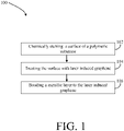
FIG. 1 illustrates a method of manufacturing an aerospace component, in accordance with various embodiments; -
FIG. 2A illustrates a step in a method of manucturing an aerospace component, in accordance with various embodiments; -
FIG. 2B illustrates a step in a method of manucturing an aerospace component, in accordance with various embodiments; -
FIG. 2C illustrates a step in a method of manucturing an aerospace component, in accordance with various embodiments; -
FIG. 2D illustrates a step in a method of manucturing an aerospace component, in accordance with various embodiments; -
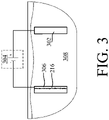
FIG. 3 illustrates a method of bonding a metallic layer to a laser induced graphene of a polymeric substrate, in accordance with various embodiments; -
FIG. 4A illustrates a system for treating a surface with laser induced graphene, in accordance with various embodiments; -
FIG. 4B illustrates a system for treating a surface with laser induced graphene, in accordance with various embodiments; and -
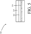
FIG. 5 illustrates a step in a method of manucturing an aerospace component, in accordance with various embodiments. - The detailed description of exemplary embodiments herein refers to the accompanying drawings, which show exemplary embodiments by way of illustration. While these exemplary embodiments are described in sufficient detail to enable those skilled in the art to practice the inventions, it should be understood that other embodiments may be realized and that logical changes and adaptations in design and construction may be made in accordance with this invention and the teachings herein. Thus, the detailed description herein is presented for purposes of illustration only and not for limitation. The scope of the invention is defined by the appended claims. For example, the steps recited in any of the method or process descriptions may be executed in any order and are not necessarily limited to the order presented. Furthermore, any reference to singular includes plural embodiments, and any reference to more than one component or step may include a singular embodiment or step. Also, any reference to attached, fixed, connected or the like may include permanent, removable, temporary, partial, full and/or any other possible attachment option. Additionally, any reference to without contact (or similar phrases) may also include reduced contact or minimal contact. Surface shading lines may be used throughout the figures to denote different parts but not necessarily to denote the same or different materials. In some cases, reference coordinates may be specific to each figure.
- In various embodiments, laser induced graphene (LIG), as disclosed herein, may comprise a low-cost, easy to implement method of incorporating graphene-like materials onto polymer composites by photothermally converting the polymer matrix at the surface to a conductive carbon. In this regard, an external laser etch could provide a facile and mechanically stable electrically conductive interface whereby traditional plating techniques could then be employed, in accordance with various embodiments. Non-line-of site areas would be accessible with the addition of specific part fixturing and reflective surfaces to reach hard to see sites, such as cylindrical inner diameter surfaces, or the like.
- In various embodiments, the manufacturing processes and systems disclosed herein can facilitate the expansion of composite components in high wear locations. In various embodiments, the manufacturing processes and systems disclosed herein are a low-cost method configured to facilitate use of traditional plating methods with a large supply chain. In various embodiments, a resultant component made from the systems and methods disclosed herein can impart electromagnetic interface (EMI) shielding for a polymeric-based component. In various embodiments, a resultant component from the manufacturing processes and systems disclosed herein can result in improved thermal transport to an external surface.
- Referring now to
FIGs. 1 and2A-2D , a method of manufacture 100 (FIG. 1 ) and an illustration of the method 100 (FIGs. 2A-2D ) are illustrated, in accordance with various embodiments.. In various embodiments, themethod 100 comprises chemically etching asurface 212 of apolymeric substrate 210 to form an etched surface 214 (step 102). In various embodiments, chemical etching in accordance withstep 102 may improve adhesion. However, the method ofmanufacture 100 can be performed withoutstep 102 and still be within the scope of this disclosure. In various embodiments, thepolymeric substrate 210 includes a thermoplastic resin. In various embodiments, the thermoplastic resin of thepolymeric substrate 210 can be either crystalline or amorphous. - Examples of the crystalline thermoplastic resin include polyester, polyolefin, polyoxymethylene (POM), polyamide (PA), poly arylene sulfide, poly ketone (PK), poly ether ketone (PEK), polyether ether ketone (PEEK), polyether ketone ketone (PEKK), polyvinylidene fluoride (PVDF), polytetrafluoroethylene (PTFE), poly aryl ether ketone (PAEK), polyether nitrile (PEN), fluor resin, and liquid crystal polymer (LCP). Examples of the polyester include polyethylene terephthalate (PET), polybutylene terephthalate (PBT), poly trimethylene terephthalate (PTT), polyethylene naphthalate (PEN), and liquid crystal polyester. Examples of the polyolefin include polyethylene (PE), polypropylene (PP), and polybutylene. Examples of the poly arylene sulfide include polyphenylene sulfide (PPS). Examples of the fluoro resin include polytetrafluoroethylene.
- Examples of the amorphous thermoplastic resin include polystyrene, polycarbonate (PC), polymethyl methacrylate (PMMA), polyvinyl chloride (PVC), polyphenylene ether (PPE), polyimide (PI), polyamide imide (PAI), polyetherimide (PEI), poly sulfone (PSU), polyether sulfone (PES), and poly arylate (PAR). The thermoplastic resin to be used for the
polymeric substrate 210 also may be phenoxy resin, polystyrene, polyolefin, polyurethane, polyester, polyamide, polybutadiene, polyisoprene, fluorine resin, acrylonitrile, and other thermoplastic elastomers, and copolymers and modified resin thereof. - In various embodiments, the
polymeric substrate 210 is electrically insulating (e.g., non-conductive) at the surface. In this regard, thepolymeric substrate 210 is limited from certain aerospace type applications due to not meeting wear or abrasion criteria, electrical bonding criteria, EMI shielding capabilities, or the like, in accordance with various embodiments. Additionally, other electrical plating methods, or processes, often result in poor or no adhesion of a metal to a polymeric substrate (e.g., polymeric substrate 210), which limits functionality of a plated polymeric substrate under higher loads associated with aerospace applications. - In various embodiments, the
method 100 further comprises treating theetched surface 214 of thepolymeric substrate 210 with a laser to induce graphene formation at the surface 216 (step 104). If the method is performed withoutstep 102, as described above, thesurface 212 of thepolymeric substrate 210 would be treated with the laser to induce graphene formation at at thesurface 216 instep 104. In various embodiments, the laser inducedgraphene 216 is performed via laser scribing (i.e., irradiation with laser pulses that transform a portion of thepolymeric substrate 210 into the laser inducedgraphene 216 via a photothermal pyrolysis process). As described further herein, a laser source can be an infrared (IR) laser source, an ultraviolet (UV) laser source, a carbon dioxide (CO2) laser source, or the like. In various embodiments, the laser source is a CO2 laser source. In this regard, a CO2 laser source can provide relatively low cost, ease of use and maintenance, and/or greater efficiency relative to alternative laser sources for treating with laser inducedgraphene 216 instep 104, in accordance with various embodiments. - In various embodiments, the laser induced
graphene 216 produced fromstep 104 comprises a first thickness T1. The first thickness can be between 1/10th thousandths of an inch (2.54 µm) to 1/50th thousandths of an inch (0.51 µm), or between 1/15th thousandths of an inch (1.69 µm) and 1/35th thousandths of an inch (0.73 µm), or approximately 1/25th thousandths of an inch (1.02 µm). However, the present disclosure is not limited in this regard and various thicknesses outside the above range are within the scope of this disclosure. In various embodiments, the laser inducedgraphene 216 is a conductive surface. In this regard, the laser inducedgraphene 216 can help facilitate a greater bond with a metal plating being applied thereon instep 106 as described further herein. - In various embodiments, the
method 100 further comprises bonding ametallic layer 218 to the laser induced graphene 216 (step 106). In various embodiments, atransition layer 217 can form between the laser inducedgraphene 216 and themetallic layer 218. Thetransition layer 217 can facilitate a stronger bond (e.g., a greater adhesion strength) between the laser inducedgraphene 216 of thepolymeric substrate 210 and themetallic layer 218 relative to a bond created without the treatingstep 104. In various embodiments, there is notransition layer 217. The present disclosure is not limited in this regard. In various embodimetns, due to the laser inducedgraphene 216 forming a conductive layer to bond with themetallic layer 218, a stronger adhesion strength is achieved relative to typical joining methods of polymeric materials to metallic layers. In various embodiments, the metallic layer can comprise any metallic layer. For example, themetallic layer 218 can comprise copper, nickel, chromium, gold, zinc, silver, platinum, palladium, rhodium, tin, cadmium, aluminum, cobalt, lead, tungsten, and alloys such as zinc-nickel, nickel phosphorous, and brass or the like. In various embodiments, themetallic layer 218 comprises nickel, or a nickel-based alloy as described further herein. In various embodiments, it may be beneficial to use more than onemetallic layer 218 to create a gradient metal layer system. This may impart benefits to the structure, such as reducing strain mismatch between themetallic layer 218 and the laser inducedgraphene 216, or allowing the outer layer to be chosen based on function, such as hardness, conductivity, inertness, decorative means, etc. For example, with reference now toFIG. 5 , a metal coated polymeric-basedcomponent 500 can comprise the laser inducedgraphene 216, themetallic layer 218, and a secondmetallic layer 501 disposed between themetallic layer 218 and the laser inducedgraphene 216. In various embodiments, a transition layer (e.g., similar to transition layer 217) can be formed between the laser inducedgraphene 216 and the secondmetallic layer 501 and between themetallic layer 218 and the secondmetallic layer 501. - In various embodiments, completion of
step 106 ofmethod 100 results in a metal coated polymeric-basedcomponent 200 is formed. In various embodiments, the metal coated polymeric-basedcomponent 200 comprises a coating thickness T2 that is between 2 and 1000 times greater than the thickness T1 of the laser inducedgraphene 216. In this regard, the coating thickness T2 can be significantly greater than the laser inducedgraphene 216. As described previously herein, the laser inducedgraphene 216 is provided to facilitate a significantly stronger bond between thepolymeric substrate 210 and themetallic layer 218 and is provided to facilitate various joining techniques (as described further herein) that are typically only utilized for joining a metal to a metal. Thus, by treating thepolymeric substrate 210 with laser induced graphene, the surface being coated with themetallic layer 218 is conductive (i.e., the laser inducedgraphene 216 is conductive), which enables less costly manufacturing methods to join the polymeric substrate to themetallic layer 218, in accordance with various embodiments. - In various embodiments, the
bonding step 106 can be performed via various methods. For example, step 106 can comprise electroplating, in accordance with various embodiments. With brief reference toFIG. 3 , electroplating themetallic layer 218 to thepolymeric substrate 210 can comprise: (a) coupling an anode 302 (e.g., made of a material that forms themetallic layer 218 inFIG. 2D ) to a positive terminal of apower source 304, (b) coupling a cathode 306 (i.e., the laser inducedgraphene 216 created from step 104) to a negative terminal of thepower source 304, (c) immersing theanode 302 and thecathode 306 in asolution 308 that contains an electrolyte (e.g., acids, bases, metal salts, molten salts, or the like), and supplying a current via thepower source 304. In this regard, once direct current is applied, theanode 302 is oxidized, metal atoms of the anode dissolve in theelectrolyte solution 308, the dissolved metal ions are reduced at thecathode 306 and from themetallic layer 218 fromFIG. 2D . In various embodiments, thesolution 308 comprises a watts bath composition (e.g., nickel sulfate, nickel chloride, and boric acid) (i.e., for brightening purposes), a nickel sulfamate bath composition (e.g., nickel sulfamate, nickel chloride, and boric acid), an all-chloride bath composition (e.g., nickel chloride and boric acid), a sulfate-chloride bath composition (e.g., nickel sulfate, nickel chloride, and boric acid), an all-sulfate bath composition (e.g., nickel sulfate and boric acid), a hard nickel bath composition (e.g., nickel sulfate, ammonium chloride, and boric acid), a black nickel bath composition (e.g., nickel ammonium sulfate, zinc sulfate, and sodium thiocyanate), or the like. The present disclosure is not limited in this regard. - Referring now to
FIG. 4A , asystem 400 for treating anexternal surface 402 of apolymeric substrate 210 to form laser inducedgraphene 216 is illustrated, in accordance with various embodiments. In various embodiments, theexternal surface 402 comprises a direct line of sight. In this regard, alaser source 410 of thesystem 400 can be directly applied to theexternal surface 402. In various embodiments, thelaser source 410 comprises an infrared (IR) laser source, an ultraviolet (UV) laser source, a carbon dioxide (CO2) laser source, or the like. In various embodiments, thelaser source 410 is a CO2 laser source. - In various embodiments, an IR laser source as referred to herein, refers to a laser source configured to emit electromagnetic radiation having an average wavelength in a range between 700 nanometers (nm) and 1 millimeter). In various embodiments, UV laser source, as disclosed herein refers to a laser source configured to emit electromagnetic radiation having an average wavelength between 100 nm and 400 nm. In various embodiments, a CO2 laser source as disclosed herein can be configured to emit a gas mixture comprising helium and carbon dioxide, and nitrogen. The gas mixture can be emitted at an average wavelength between 10 and 11 micrometers (µm). In various embodiments, the carbon dioxide is the laser-active medium, the nitrogen creates energy to facilitate excitation, and helium ensures dissipation of heat.
- Referring now to
FIG. 4B , asystem 500 for treating an internal surface 502 (e.g., an inner diameter surface of a cylinder, a pipe, or the like) of a polymeric based component 420 (e.g., made of a polymeric substrate 210) is illustrated, in accordance with various embodiments. Thesystem 500 includes thelaser source 410 and a reflective component 420 (e.g., a mirror, a component with a highly reflective coating, or the like). Anyreflective component 420 is within the scope of this disclosure. In various embodiments, any of thelaser source 410, thereflective component 420 or the polymeric-based component receiving the laser treatment ofstep 104 can be configured to move relative to the other components. In this regard, thelaser source 410 can move relative to thereflective component 420 and/or the polymeric basedcomponent 430, thereflective component 420 can be configured to move relative to thelaser source 410 and/or the polymeric basedcomponent 430, the polymeric basedcomponent 430 can be configured to move relative to thelaser source 410 and/or thereflective component 420, or any combination of the above. - In various embodiments, as described previously herein, the laser induced graphene treatment of
step 104 facilitates a strong bond between apolymeric substrate 210 and ametallic layer 218. In various embodiments, the strong adhesion strength of thetransition layer 217 fromFIG. 2D facilitates use of themethod 100 on aerospace grade polymeric materials that are electrically insulating. In this regard, a conductive coating can be applied to apolymeric substrate 210 via themethod 100 fromFIG. 1 , and thecomponent 200 fromFIG. 2D can have weight saving benefits of being made mostly of a polymeric material, maintain electrical bonding criteria for the component, and/or be capable of enduring higher loads at a lower manufacturing cost relative to typical bonding methods of a polymeric substrate to a metallic layer, in accordance with various embodiments. - Benefits, other advantages, and solutions to problems have been described herein with regard to specific embodiments. Furthermore, the connecting lines shown in the various figures contained herein are intended to represent exemplary functional relationships and/or physical couplings between the various elements. It should be noted that many alternative or additional functional relationships or physical connections may be present in a practical system. However, the benefits, advantages, solutions to problems, and any elements that may cause any benefit, advantage, or solution to occur or become more pronounced are not to be construed as critical, required, or essential features or elements of the inventions. The scope of the inventions is accordingly to be limited by nothing other than the appended claims, in which reference to an element in the singular is not intended to mean "one and only one" unless explicitly so stated, but rather "one or more." Moreover, where a phrase similar to "at least one of A, B, or C" is used in the claims, it is intended that the phrase be interpreted to mean that A alone may be present in an embodiment, B alone may be present in an embodiment, C alone may be present in an embodiment, or that any combination of the elements A, B and C may be present in a single embodiment; for example, A and B, A and C, B and C, or A and B and C. Different cross-hatching is used throughout the figures to denote different parts but not necessarily to denote the same or different materials.
- Systems, methods, and apparatus are provided herein. In the detailed description herein, references to "one embodiment," "an embodiment," "an example embodiment," etc., indicate that the embodiment described may include a particular feature, structure, or characteristic, but every embodiment may not necessarily include the particular feature, structure, or characteristic. Moreover, such phrases are not necessarily referring to the same embodiment. Further, when a particular feature, structure, or characteristic is described in connection with an embodiment, it is submitted that it is within the knowledge of one skilled in the art to affect such feature, structure, or characteristic in connection with other embodiments whether or not explicitly described. After reading the description, it will be apparent to one skilled in the relevant art(s) how to implement the disclosure in alternative embodiments. Furthermore, no element, component, or method step in the present disclosure is intended to be dedicated to the public regardless of whether the element, component, or method step is explicitly recited in the claims. No claim element is intended to invoke 35 U.S.C. 112(f) unless the element is expressly recited using the phrase "means for." As used herein, the terms "comprises," "comprising," or any other variation thereof, are intended to cover a non-exclusive inclusion, such that a process, method, article, or apparatus that comprises a list of elements does not include only those elements but may include other elements not expressly listed or inherent to such process, method, article, or apparatus.
Claims (15)
- A method of manufacture, the method comprising:treating a surface of a polymeric substrate (210) with a laser to form a porous graphene at the surface; andbonding a metallic layer (218) to the porous graphene.
- The method of claim 1, wherein the surface is an internal surface of an aerospace component, and wherein bonding the metallic layer (218) comprises electroplating.
- The method of claim 1 or 2, wherein the surface of the polymeric substrate (210) is non-conductive.
- The method of any preceding claim, wherein treating the surface with the porous graphene further comprises laser scribing the surface with a carbon dioxide laser source.
- The method of any preceding claim, wherein a first thickness of the metallic layer (218) is at least 2 times a second thickness of the porous graphene.
- The method of any preceding claim, further comprising bonding a second metallic layer (501) to the metallic layer, and optionally wherein the metallic layer (218) is a different material than the second metallic layer (501).
- A method of manufacturing an aerospace component, the method comprising:reflecting a laser beam from a laser source via a reflective component;laser scribing an internal surface of a polymeric component in response to reflecting the laser beam;forming laser induced graphene on the internal surface in response to laser scribing the internal surface; andbonding a metallic layer (218) to the laser induced graphene.
- The method of manufacture of claim 7, wherein bonding the metallic layer (218) includes electroplating.
- The method of manufacture of claim 7, wherein the laser beam includes a gas mixture comprising carbon dioxide.
- The method of manufacture of claim 9, wherein the gas mixture further comprises helium and nitrogen, and/or wherein an average wavelength of the laser beam is between 10 micrometers and 11 micrometers.
- The method of any of claims 7 to 10, wherein bonding the metallic layer (218) further comprises electrically coupling an anode having a metallic material to a positive terminal of a power source, coupling the laser induced graphene to a negative terminal of the power source, disposing the anode and the polymeric component in an electrolyte solution, and supplying a current via the power source, and optionally wherein the metallic layer (218) comprises at least one of nickel, copper, chromium, gold, zinc, silver, platinum, palladium, rhodium, tin, cadmium, aluminum, cobalt, lead, tungsten, zinc-nickel, nickel phosphorus, and brass.
- The method of any of claims 7 to 11, further comprising bonding a second metallic layer (501) to the metallic layer (218), and optionally wherein the metallic layer (218) is a different material than the second metallic layer.
- An aerospace component, comprising:a polymeric material comprising an external and an internal surface including a laser induced graphene thereon; anda metallic coating coupled to at least one of the external and the internal surface.
- The aerospace component of claim 13, wherein the metallic coating comprises at least one of nickel, copper, chromium, gold, zinc, silver, platinum, palladium, rhodium, tin, cadmium, aluminum, cobalt, lead, tungsten, zinc-nickel, nickel phosphorus, and brass.
- The aerospace component of claim 13 or 14, wherein the internal surface is an inner diameter surface of a shock strut or actuator piston, and/or further comprising a metallic layer (218) disposed between the metallic coating and the laser induced graphene.
Applications Claiming Priority (2)
| Application Number | Priority Date | Filing Date | Title |
|---|---|---|---|
| US202163188769P | 2021-05-14 | 2021-05-14 | |
| US17/733,792 US12269743B2 (en) | 2021-05-14 | 2022-04-29 | Laser induced graphene as pretreatment to plate non-conductive composites |
Publications (1)
| Publication Number | Publication Date |
|---|---|
| EP4089209A1 true EP4089209A1 (en) | 2022-11-16 |
Family
ID=81648429
Family Applications (1)
| Application Number | Title | Priority Date | Filing Date |
|---|---|---|---|
| EP22173102.9A Pending EP4089209A1 (en) | 2021-05-14 | 2022-05-12 | Laser induced graphene as pretreatment to plate non-conductive composites |
Country Status (4)
| Country | Link |
|---|---|
| US (2) | US12269743B2 (en) |
| EP (1) | EP4089209A1 (en) |
| BR (1) | BR102022009394A2 (en) |
| CA (1) | CA3159921A1 (en) |
Families Citing this family (2)
| Publication number | Priority date | Publication date | Assignee | Title |
|---|---|---|---|---|
| CN116216700B (en) * | 2023-02-11 | 2026-01-30 | 南京农业大学 | A method for preparing graphene materials using polymer powder |
| CN116216699B (en) * | 2023-02-11 | 2025-07-18 | 南京农业大学 | Method for preparing graphene material by using waste mask |
Citations (1)
| Publication number | Priority date | Publication date | Assignee | Title |
|---|---|---|---|---|
| CN111383991A (en) * | 2020-03-19 | 2020-07-07 | 张宇明 | A kind of conductive hole and its preparation method and application |
Family Cites Families (5)
| Publication number | Priority date | Publication date | Assignee | Title |
|---|---|---|---|---|
| WO2015175060A2 (en) | 2014-02-17 | 2015-11-19 | William Marsh Rice University | Laser induced graphene materials and their use in electronic devices |
| US9926427B2 (en) | 2015-12-10 | 2018-03-27 | Nanotek Instruments, Inc. | Chemical-free production of graphene-reinforced polymer matrix composites |
| WO2017223217A1 (en) | 2016-06-21 | 2017-12-28 | William Marsh Rice University | Laser-induced graphene scrolls (ligs) materials |
| WO2020021361A1 (en) | 2018-07-23 | 2020-01-30 | King Abdullah University Of Science And Technology | Lignin based laser lithography process for fabricating 3d graphene electrode and method |
| US12227420B2 (en) | 2018-12-28 | 2025-02-18 | B.G. Negev Technologies And Application Ltd., At Ben-Gurion U Suniversity State Or Country) | Laser-induced graphene sensors and methods of making and using same |
-
2022
- 2022-04-29 US US17/733,792 patent/US12269743B2/en active Active
- 2022-05-12 CA CA3159921A patent/CA3159921A1/en active Pending
- 2022-05-12 EP EP22173102.9A patent/EP4089209A1/en active Pending
- 2022-05-13 BR BR102022009394-6A patent/BR102022009394A2/en unknown
-
2025
- 2025-03-03 US US19/068,949 patent/US20250243069A1/en active Pending
Patent Citations (1)
| Publication number | Priority date | Publication date | Assignee | Title |
|---|---|---|---|---|
| CN111383991A (en) * | 2020-03-19 | 2020-07-07 | 张宇明 | A kind of conductive hole and its preparation method and application |
Non-Patent Citations (1)
| Title |
|---|
| YIN JUN ET AL: "Flexible 3D porous graphene film decorated with nickel nanoparticles for absorption-dominated electromagnetic interference shielding", CHEMICAL ENGENEERING JOURNAL, ELSEVIER, AMSTERDAM, NL, vol. 421, 18 April 2021 (2021-04-18), XP086628564, ISSN: 1385-8947, [retrieved on 20210418], DOI: 10.1016/J.CEJ.2021.129763 * |
Also Published As
| Publication number | Publication date |
|---|---|
| US20250243069A1 (en) | 2025-07-31 |
| US20220363545A1 (en) | 2022-11-17 |
| US12269743B2 (en) | 2025-04-08 |
| BR102022009394A2 (en) | 2022-11-22 |
| CA3159921A1 (en) | 2022-11-14 |
Similar Documents
| Publication | Publication Date | Title |
|---|---|---|
| US20250243069A1 (en) | Laser induced graphene as pretreatment to plate non-conductive composites | |
| KR102029648B1 (en) | Metal sheet for separators of polymer electrolyte fuel cells, and metal sheet for manufacturing the same | |
| CA2880378C (en) | Modified shank fasteners for electromagnetic effect (eme) technology | |
| CN102985765A (en) | Renewable energy source including an energy conversion structure and a bearing component | |
| KR960030457A (en) | METHOD FOR MANUFACTURING POROUS MATERIAL, METHOD FOR MANUFACTURING ELECTRODE SUBSTRATE FOR BATTERY, | |
| EP2132817A1 (en) | Process for the preparation of electrodes for use in a fuel cell | |
| US20110165501A1 (en) | Fuel cell separator and fuel cell | |
| Yeh et al. | Application of porous oxide layer in plastic/metal direct adhesion by injection molding | |
| CN111527618A (en) | Battery cell with aluminum casing | |
| JP2008094923A (en) | Surface modification method for cycloolefin polymer material, surface modified cycloolefin polymer material obtained by using the method, method for forming metal film on the surface modified cycloolefin polymer material, and cycloolefin polymer material with metal film | |
| CN108963266A (en) | A kind of collector of lithium ion battery and preparation method thereof | |
| JP7502004B2 (en) | Compositions and methods for activating titanium substrates | |
| Wang et al. | Communication—Ag NW networks enhanced by Ni electroplating for flexible transparent electrodes | |
| García et al. | Polymer-based additive manufacturing of a complex RF front-end for new space applications | |
| Zhou et al. | Chemically activated Ag-embedded bridged-layer for copper pattern addition on PET film | |
| JP2009295295A (en) | Water cool-type bus bar and method of manufacturing the same | |
| EP4540531A1 (en) | Blind fastener | |
| US20150195897A1 (en) | Apparatus having management of electrical power capacity regions and management of thermal capacity regions | |
| CN109713836A (en) | A kind of motor central spindle, the processing method of motor and motor central spindle | |
| CN224001548U (en) | High-temperature alloy chromeplate clamp | |
| JP5413050B2 (en) | Manufacturing method of fuel cell separator | |
| US20050156596A1 (en) | Gradient coil and method for construction | |
| KR102827548B1 (en) | Structural battery having a single fastening structure capable of mechanical fastening and electrical connection at the same time and manufacturing method thereof | |
| RU2858059C2 (en) | Resistive flexible heating element current supply device | |
| CN220774420U (en) | Current collector and electrode plate |
Legal Events
| Date | Code | Title | Description |
|---|---|---|---|
| PUAI | Public reference made under article 153(3) epc to a published international application that has entered the european phase |
Free format text: ORIGINAL CODE: 0009012 |
|
| STAA | Information on the status of an ep patent application or granted ep patent |
Free format text: STATUS: THE APPLICATION HAS BEEN PUBLISHED |
|
| AK | Designated contracting states |
Kind code of ref document: A1 Designated state(s): AL AT BE BG CH CY CZ DE DK EE ES FI FR GB GR HR HU IE IS IT LI LT LU LV MC MK MT NL NO PL PT RO RS SE SI SK SM TR |
|
| STAA | Information on the status of an ep patent application or granted ep patent |
Free format text: STATUS: REQUEST FOR EXAMINATION WAS MADE |
|
| 17P | Request for examination filed |
Effective date: 20230516 |
|
| RBV | Designated contracting states (corrected) |
Designated state(s): AL AT BE BG CH CY CZ DE DK EE ES FI FR GB GR HR HU IE IS IT LI LT LU LV MC MK MT NL NO PL PT RO RS SE SI SK SM TR |
|
| P01 | Opt-out of the competence of the unified patent court (upc) registered |
Effective date: 20230922 |