EP4087111A1 - Charger and control method - Google Patents
Charger and control method Download PDFInfo
- Publication number
- EP4087111A1 EP4087111A1 EP20911797.7A EP20911797A EP4087111A1 EP 4087111 A1 EP4087111 A1 EP 4087111A1 EP 20911797 A EP20911797 A EP 20911797A EP 4087111 A1 EP4087111 A1 EP 4087111A1
- Authority
- EP
- European Patent Office
- Prior art keywords
- control unit
- side switch
- turned
- control
- control signal
- Prior art date
- Legal status (The legal status is an assumption and is not a legal conclusion. Google has not performed a legal analysis and makes no representation as to the accuracy of the status listed.)
- Pending
Links
Images



Classifications
-
- H—ELECTRICITY
- H02—GENERATION; CONVERSION OR DISTRIBUTION OF ELECTRIC POWER
- H02M—APPARATUS FOR CONVERSION BETWEEN AC AND AC, BETWEEN AC AND DC, OR BETWEEN DC AND DC, AND FOR USE WITH MAINS OR SIMILAR POWER SUPPLY SYSTEMS; CONVERSION OF DC OR AC INPUT POWER INTO SURGE OUTPUT POWER; CONTROL OR REGULATION THEREOF
- H02M3/00—Conversion of DC power input into DC power output
- H02M3/22—Conversion of DC power input into DC power output with intermediate conversion into AC
- H02M3/24—Conversion of DC power input into DC power output with intermediate conversion into AC by static converters
- H02M3/28—Conversion of DC power input into DC power output with intermediate conversion into AC by static converters using discharge tubes with control electrode or semiconductor devices with control electrode to produce the intermediate AC
- H02M3/325—Conversion of DC power input into DC power output with intermediate conversion into AC by static converters using discharge tubes with control electrode or semiconductor devices with control electrode to produce the intermediate AC using devices of a triode or a transistor type requiring continuous application of a control signal
- H02M3/335—Conversion of DC power input into DC power output with intermediate conversion into AC by static converters using discharge tubes with control electrode or semiconductor devices with control electrode to produce the intermediate AC using devices of a triode or a transistor type requiring continuous application of a control signal using semiconductor devices only
- H02M3/33507—Conversion of DC power input into DC power output with intermediate conversion into AC by static converters using discharge tubes with control electrode or semiconductor devices with control electrode to produce the intermediate AC using devices of a triode or a transistor type requiring continuous application of a control signal using semiconductor devices only with automatic control of the output voltage or current, e.g. flyback converters
- H02M3/33523—Conversion of DC power input into DC power output with intermediate conversion into AC by static converters using discharge tubes with control electrode or semiconductor devices with control electrode to produce the intermediate AC using devices of a triode or a transistor type requiring continuous application of a control signal using semiconductor devices only with automatic control of the output voltage or current, e.g. flyback converters with galvanic isolation between input and output of both the power stage and the feedback loop
-
- H—ELECTRICITY
- H02—GENERATION; CONVERSION OR DISTRIBUTION OF ELECTRIC POWER
- H02M—APPARATUS FOR CONVERSION BETWEEN AC AND AC, BETWEEN AC AND DC, OR BETWEEN DC AND DC, AND FOR USE WITH MAINS OR SIMILAR POWER SUPPLY SYSTEMS; CONVERSION OF DC OR AC INPUT POWER INTO SURGE OUTPUT POWER; CONTROL OR REGULATION THEREOF
- H02M1/00—Details of apparatus for conversion
- H02M1/0003—Details of control, feedback or regulation circuits
-
- H—ELECTRICITY
- H02—GENERATION; CONVERSION OR DISTRIBUTION OF ELECTRIC POWER
- H02M—APPARATUS FOR CONVERSION BETWEEN AC AND AC, BETWEEN AC AND DC, OR BETWEEN DC AND DC, AND FOR USE WITH MAINS OR SIMILAR POWER SUPPLY SYSTEMS; CONVERSION OF DC OR AC INPUT POWER INTO SURGE OUTPUT POWER; CONTROL OR REGULATION THEREOF
- H02M3/00—Conversion of DC power input into DC power output
- H02M3/22—Conversion of DC power input into DC power output with intermediate conversion into AC
- H02M3/24—Conversion of DC power input into DC power output with intermediate conversion into AC by static converters
- H02M3/28—Conversion of DC power input into DC power output with intermediate conversion into AC by static converters using discharge tubes with control electrode or semiconductor devices with control electrode to produce the intermediate AC
- H02M3/325—Conversion of DC power input into DC power output with intermediate conversion into AC by static converters using discharge tubes with control electrode or semiconductor devices with control electrode to produce the intermediate AC using devices of a triode or a transistor type requiring continuous application of a control signal
- H02M3/335—Conversion of DC power input into DC power output with intermediate conversion into AC by static converters using discharge tubes with control electrode or semiconductor devices with control electrode to produce the intermediate AC using devices of a triode or a transistor type requiring continuous application of a control signal using semiconductor devices only
- H02M3/33569—Conversion of DC power input into DC power output with intermediate conversion into AC by static converters using discharge tubes with control electrode or semiconductor devices with control electrode to produce the intermediate AC using devices of a triode or a transistor type requiring continuous application of a control signal using semiconductor devices only having several active switching elements
- H02M3/33573—Full-bridge at primary side of an isolation transformer
Definitions
- Embodiments of the present application relate to the field of charging technology, and more particularly, to a charger and a control method thereof.
- a charger is generally composed of a transformer, a control unit, a drive unit, a MOS tube, etc.
- Embodiments of the present application provides a charger and a control method to solve the problems existing in the related art.
- a first aspect provides a charger comprising: a transformer; at least one primary-side switch tube configured to perform chopping modulation for a voltage input into the transformer; a first control unit; a second control unit configured to acquire information of a voltage and/or current output from an output end of the charger; and a first microwave unit connected to the first control unit and the second control unit respectively and configured to transmit the information of a voltage and/or current to the first control unit; wherein the first control unit is configured to output a first control signal according to the information of a voltage and/or current, so as to control the at least one primary-side switch tube to be turned on or turned off.
- a second aspect provides a charger comprising: a transformer; at least one primary-side switch tube connected to a primary side of the transformer; at least one secondary-side switch tube connected to a secondary side of the transformer; a first control unit configured to output a first control signal, wherein the first control signal is configured to control the at least one primary-side switch tube to be turned on or turned off; a second control unit configured to output a second control signal, wherein the second control signal is configured to control the at least one secondary-side switch tube to be turned on or turned off; and a first microwave unit connected to the first control unit and the second control unit respectively and configured to transmit a synchronization signal between the first control unit and the second control unit, wherein the synchronization signal is configured to synchronize the first control signal and the second control signal.
- a third aspect provides a control method, the control method is applicable to a charger, the charger comprises a transformer, at least one primary-side switch tube, a first control unit, a second control unit, and a first microwave unit; the method comprises: the second control unit acquiring information of a voltage and/or current output from an output end of the charger; the first microwave unit transmitting the information of a voltage and/or current to the first control unit; and the first control unit outputting a first control signal according to the information of a voltage and/or current to control the at least one primary-side switch tube to be turned on or turned off.
- a fourth aspect provides a control method, the control method is applicable to a charger, the charger comprises a transformer, at least one primary-side switch tube, at least one secondary-side switch tube, a first control unit, a second control unit, and a first microwave unit; the method comprises: the first control unit outputting a first control signal, wherein the first control signal is configured to control the at least one primary-side switch tube to be turned on or turned off; the second control unit outputting a second control signal, wherein the second control signal is configured to control the at least one secondary-side switch tube to be turned on or turned off; and the first microwave unit transmitting a synchronization signal between the first control unit and the second control unit, wherein the synchronization signal is configured to synchronize the first control signal and the second control signal.
- a fifth aspect provides a computer-readable storage medium configured to store a computer program, wherein the computer program enables a computer to execute a method according to the above third aspect, or fourth aspect, or any one of their implementation manners.
- a sixth aspect provides a computer program product, characterized by comprising computer program instructions, wherein the computer program instructions enable a computer to execute a method according to the above third aspect, or fourth aspect, or any one of their implementation manners.
- a first transmitting end of the first microwave unit can convert a first control signal into a first microwave signal and transmit the first microwave signal to a first receiving end of the first microwave unit; after the first receiving end receives the first microwave signal, the first microwave signal can be converted into the first control signal, such that the converted first control signal can be used to control the at least one first switch tube to be turned on and turned off.
- the first transmitting end thereof can convert the first control signal into the first microwave signal and quickly transmit it to the first receiving end of the first microwave unit, a driving speed is fast, and dead time can be controlled accurately; even in the condition that dead time of the first control signal is short, the first switch tube can still be quickly turned on or turned off, crosstalk of circuit will not be caused.
- transmission of microwaves does not dependent on transmission in media, a distance between the first transmitting end and the first receiving end of the first microwave unit can be set to be far, transmission of parasitic capacitance generated by the first switch tube can be insulated, and thus crosstalk of circuit can also be avoided.
- Power supply conversion equipment for small portable electronic equipment and electronic appliances are generally composed of shells, transformers, inductors, capacitors, control ICs, PCB boards and other components, and used to convert AC input into DC output.
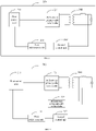
- a charger can include a primary control module 111, a secondary control module 112, a primary driving unit 121, a synchronous rectification driving unit 122, a primary-side switch tube 131, a secondary-side switch tube 132, a transformer 140, and an optocoupler (which may also be referred to as a photoelectric coupler or a photoelectric isolator) 150.
- the primary-side switch tube 131 can be used to perform rectification filtering, chopping modulation, and so on for AC current input to the charger.
- the secondary-side switch tube 132 can be used to synchronously rectify current output by the transformer 140.
- the secondary control module 112 can be used to obtain information of a voltage/current output by the transformer 140, or obtain information of a voltage/current output by an output terminal of the charger, and transmit error information (for example, the error information can be a difference value between information of actually output a voltage/current and information of required a voltage/current) to the primary control module 111 through the optocoupler 150.
- the primary control module 111 can convert the error information into a duty ratio or frequency of a PWM control signal, and output the PWM control signal to the primary driving unit 121 to drive the primary-side switch tube 131.
- the synchronous rectification driving unit 122 is used to drive the secondary-side switch tube 132 so that the secondary-side switch tube 132 performs synchronous rectification.
- the primary control module 111 can output a corresponding PWM signal according to the above error information to control the secondary drive unit 123, thereby driving the secondary-side switch tube 132.
- the primary side switch 131 may include one or more metal oxide semiconductor field effect transistors (MOSFET), i.e., MOS transistors; for example, the primary side switch 131 may include two MOS transistors or four MOS transistors.
- MOSFET metal oxide semiconductor field effect transistors
- the secondary-side switch tube 132 may also include one or more MOS transistors, for example, the secondary-side switch tube 132 may include one MOS transistor or two MOS transistors.
- Electronic devices in embodiments of the present application may include, but are not limited to, a satellite or cellular telephone; a personal communication system (PCS) terminal that can combine cellular radio telephones with data processing, facsimile and data communication capabilities; a personal digital assistant (PDA) that may include a radio telephone, a pager, Internet/intranet access, a Web browser, a notepad, a calendar, and/or a Global Positioning System (GPS) receiver; conventional laptop and/or palm-sized receivers; or other electronic devices including radio telephone transceivers.
- a device to be charged may refer to a mobile terminal device or a handheld terminal device, such as a mobile phone, a pad, and the like.
- a device to be charged mentioned in these embodiments of the present application may refer to a chip system, and in these embodiments, a battery of the device to be charged may belong to or may also not belong to the chip system.
- electronic devices may also include other devices to be charged that have charging requirements, such as mobile phones, mobile power sources (e.g., power banks, travel chargers, etc.), electric vehicles, laptops, drones, tablet computers, e-books, e-cigarettes, smart devices to be charged, small electronic products, etc.
- the smart devices to be charged may include, for example, watches, wristbands, smart glasses, cleaning robots, etc.
- the small electronic products may include, for example, wireless earphones, Bluetooth speakers, electric toothbrushes, rechargeable wireless mice. etc.
- a charger provided by the present application adopts a microwave unit to perform transmission of a control signal, so as to improve a driving speed and realize accurate control of dead time. Moreover, when a control module outputs a high-frequency control signal, dead time of the control signal can be set to be short, such that efficiency can be improved and crosstalk of circuit will not be affected at the same time.
- a first microwave unit to control a first switch tube to be turned on and turned off a distance between a first transmitting end and a first receiving end thereof can be set to be far, transmission of parasitic capacitance generated by the first switch tube can be avoided, and thus crosstalk of circuit can also be avoided.
- a charger provided by an embodiment of the present application is introduced in detail below with reference to FIG. 2 .
- a charger 200 provided in this embodiment of the present application can include a first control unit 211, a second control unit 212, a first microwave unit 221, at least one first switch tube 231, and a transformer 240.
- the at least one primary-side switch tube 231 is used to perform chopping modulation for a voltage input to the transformer 240.
- the at least one primary-side switch tube 231 in this embodiment of the present application can be used to perform chopping modulation for the voltage input to the transformer 240, for example, a magnitude of a voltage of DC current output by a secondary-side of the transformer 240 can be changed by controlling and adjusting a duty ratio of the primary-side switch tube 231.
- the second control unit 212 is used to generate feedback information based on information of a voltage and/or current output from an output end of the charger 200.
- the first microwave unit 221 is connected to the first control unit 211 and the second control unit 212 respectively, and is used to transmit the feedback information to the first control unit 211.
- the first microwave unit 221 in this embodiment of the present application can transmit the feedback information acquired by the second control unit 212 to the first control unit 211.
- the feedback information may be an actual a voltage value and/or current value at the output end of the charger, or may be a difference value between an actual output a voltage value and/or current value and an expected received a voltage value and/or current value.
- the first control unit 211 is used to output a first control signal according to the feedback information to control the at least one primary-side switch tube 231 to be turned on or turned off.
- the feedback information output from the output end of the charger 200 can be feedbacked into the first control unit 211 through the first microwave unit 221 by the second control unit 212, and the first control unit 211 can output a first control signal according to the feedback information to control the at least one primary-side switch tube 231 to be turned on or turned off.
- a first transmitting end of the first microwave unit can convert a first control signal into a first microwave signal and transmit the first microwave signal to a first receiving end of the first microwave unit; after the first receiving end receives the first microwave signal, the first microwave signal can be converted into the first control signal, such that the converted first control signal can be used to control the at least one first switch tube to be turned on and turned off.
- the first transmitting end thereof can convert the first control signal into the first microwave signal and quickly transmit it to the first receiving end, a driving speed is fast, and dead time can be controlled accurately; even in the condition that dead time of the first control signal is short, the first switch tube can still be quickly turned on or turned off, crosstalk of circuit will not be caused.
- transmission of microwaves does not dependent on transmission in media, a distance between the first transmitting end and the first receiving end of the first microwave unit can be set to be far, transmission of parasitic capacitance generated by the first switch tube can be insulated, and thus crosstalk of circuit can also be avoided.
- the charger 200 can further include at least one secondary-side switch tube 232.
- the at least one secondary-side switch tube 232 is used to synchronously rectify the voltage output by the transformer 240; the first control unit is further used to output a second control signal to control the at least one secondary-side switch tube 231 to be turned on or turned off.
- the first control unit 211 is further used to output the second control signal according to the information of a voltage/or current, so as to control the at least one secondary-side switch tube 231 to be turned on or turned off.
- the charger 200 can further include at least one secondary-side switch tube 232, and the secondary-side switch tube 232 can synchronously rectify the voltage output by the transformer 240.
- the feedback information in this embodiment of the present application is a voltage difference and/or a current difference of the DC current output by the transformer 240
- the voltage difference may be a difference between a voltage actually output by a secondary-side of the transformer 240 and a voltage expected to be received
- the current difference may be a difference between current actually output by the secondary-side of the transformer 240 and current expected to be received.
- a voltage difference of feedback DC current received by the first control unit 211 is negative, it means that a voltage value output by the secondary-side of the transformer 240 is small at this time, and the first control unit 211 can control to increase output duration of a high electric level within one cycle, such that duration when the primary-side switch tube 231 is in a conducting state is increased, and thus the voltage value of the DC current output by the secondary-side of the transformer is increased;
- the voltage difference of the feedback DC current received by the first control unit 211 is positive, it means that the voltage value output by the secondary-side of the transformer 240 is great at this time, and the first control unit 211 can control to reduce the output duration of the high electric level within one cycle, such that the duration when the primary-side switch tube 231 is in a conducting state is reduced, and thus the voltage value of the DC current output by the secondary-side of the transformer is reduced.
- the feedback information in this embodiment of the present application can also be a voltage value and/or a current value of the DC current output by the secondary-side of the transformer 240
- the first microwave unit 221 can feedback the voltage value and/or the current value to the first control unit 211
- the first control unit 211 can compare a received a voltage value and/or current value with a preset a voltage value and/or current value.
- the first control unit 211 can control to increase output duration of a high electric level within one cycle, such that duration when the primary-side switch tube 231 is in a conducting state is increased, and thus the voltage value of the DC current output by the secondary-side of the transformer is increased; after the feedbacked a voltage value of the DC current received by the first control unit 211 is compared with the preset a voltage value, if it is determined that the voltage value of the DC current output by the secondary-side of the transformer is greater at this time, the first control unit 211 can control to reduce the output duration of the high electric level within one cycle, such that duration when the primary-side switch tube 231 is in a conducting state is reduced, and thus the voltage value of the DC current output by the secondary-side of the transformer is reduced.
- conduction time of the at least one primary-side switch tube 231 may have association relation with the DC current output by the secondary-side of the transformer 240, that is, the longer the conduction time of the at least one primary-side switch tube 231, the larger the DC current output by the secondary-side of the transformer 240; the shorter the conduction time of the at least one primary-side switch tube 231, the smaller the DC current output by the secondary-side of the transformer 240.
- the first microwave unit 221 can also include a transmitting end and a receiving end, the transmitting end of the first microwave unit 222 can convert a digital signal sent from the second control unit 212 into a microwave signal and transmit it to a receiving end of the first microwave unit 211. After a third receiving end receives the microwave signal, the microwave signal can be converted into a digital signal and sent to the first control unit 211, so that the first control unit 211 can control output time of a high electric level and/or a low electric level of a first control signal based on the received signal.
- the charger 200 can further include a second microwave unit 222 and a first driving module 251.
- the second microwave unit 222 is connected to the first control unit.
- the first driving module 251 is connected to the first control unit and the at least one primary-side switch tube respectively.
- the second microwave unit 222 is used to transmit the first control signal output by the first control unit 211 to the first driving module 251, thereby enabling the first driving module 251 to drive the at least one primary-side switch tube 231 to be turned on or turned off.
- the charger 200 in this embodiment of the present application can further include the second microwave unit 222 and the first driving module 251, a transmitting end of the second microwave unit 222 can perform conversion for the first control signal output by the first control unit 211, convert it to a microwave signal and transmit it to a receiving end of the second microwave unit 222; when the receiving end receives the microwave signal, it can be converted into the first control signal, and the first control signal is transmitted to the first driving module 251, such that the at least one primary-side switch tube can be driven or controlled to be turned on or turned off.
- the charger 200 can further include a third microwave unit 223 and a second driving module 252.
- the third microwave unit 223 is connected to the first control unit 211.
- the second driving module 252 is connected to the third microwave unit 223 and the at least one secondary-side switch tube 232 respectively.
- the third microwave unit 223 is used to transmit a second control signal output by the first control unit 211 to the second driving module 252, thereby enabling the second driving module 252 to drive the at least one secondary-side switch tube 232 to be turned on or turned off.
- the first control unit 211 can also control at least one secondary-side switch tube 232 to be turned on or turned off; for example, by a transmitting end of the third microwave unit 223, the control signal output by the first control unit 211 can be converted; it is converted into a microwave signal and transmitted to a receiving end of the second microwave unit 222; the receiving end receives the microwave signal and can convert it into the control signal, and the control signal is transmitted to the second driving module 252, such that at least one secondary-side switch tubed can be driven or controlled to be turned on or turned off.
- FIG. 6a and FIG. 6b respectively.
- the driving circuit 200 can further include the first driving module 251 and the second driving module 252.
- the first driving module 251 can amplify a control signal output by the receiving end of the first microwave unit 221, so that the amplified signal can control the primary-side switch tube 231 to be turned on or turned off;
- the second driving module 252 can amplify a control signal output by the third microwave unit 223, so that the amplified signal can control the secondary-side switch tube 232 to be turned on or turned off.
- first driving module 251 and/or the second driving module 252 in the embodiment of the present application can be used to amplify the control signal output by the first control unit 211, that is, control capability of the control signal can be increased, so that it can control the switch tubes.
- the driving modules in this embodiment of the present application may be charge pump bootstrap control circuits, control chips, and so on.
- FIG. 6b is a structural schematic diagram of a charger provided by another embodiment of the present application.
- the first control unit 211 can control output time of a high electric level and/or a low electric level of the first control signal according to the received feedback information, so that the second driving module 252 can determine whether to send a driving signal to turn on at least one second switch tube 232 according to whether at least one switch tube 231 connected to the primary-side of the transformer is turned on.
- the second driving module 252 in this embodiment of the present application may be a synchronous rectification driving unit.
- At least one driving unit may also be included in FIGS. 2 to 4 .
- the driving unit may be located between the first control unit 211 and at least one primary-side switch tube 231 to amplify the control signal output by the first control unit 211, so that it can control at least one primary-side switch tube 231.
- two driving units can be included; wherein one driving unit may be located between the first control unit 211 and the primary-side switch tube 231 to amplify the control signal output by the first control unit 211, so that it can control the primary-side switch tube 231; the other driving unit may be located between the first control unit 211 and at least one secondary-side switch tube 232 to amplify the control signal output by the first control unit 211, so that it can control the at least one secondary-side switch tube 232.
- a transmitting end of a microwave unit in an embodiment of the present application can convert a control signal into a microwave signal, and transmit the microwave signal to a receiving end, and the receiving end can convert the microwave signal into the control signal to control a switching tube to be turned on or turned off, so that a transformer connected to the switch tube can continuously store and release energy.
- the microwave unit in this embodiment of the present application can also be used to isolate parasitic capacitance generated by the switch tube, which will be described in detail below.
- the second microwave unit 222 is further used to transmit the first control signal to control the at least one primary-side switch tube 231 to be turned on or turned off, and isolate parasitic capacitance generated by the at least one primary-side switch tube 231.
- the third microwave unit 223 is further used to transmit the second control signal to control the at least one secondary-side switch tube 232 to be turned on or turned off, and isolate parasitic capacitance generated by the at least one secondary-side switch tube 232.
- the first control unit 211 can output a high electric level signal and transmit the signal to at least one primary-side switch tube 231 through the second microwave unit 222 to control the primary-side switch tube 231 to be turned on; the first control unit 211 can also output a high electric level signal and transmit the signal to at least one secondary-side switch tube 232 through the third microwave unit 223 to control the secondary-side switch tube 232 to be turned on.
- a primary-side of the transformer 240 may refer to a side connected to at least one primary-side switch tube 231, and a secondary side of the transformer 240 may refer to a side connected to at least one secondary-side switch tube 232.
- the second microwave unit 222 in this embodiment of the present application can also isolate parasitic capacitance generated by at least one primary-side switch tube 231, that is, the parasitic capacitance generated by the at least one primary-side switch tube 231 can be isolated from being transmitted to other circuit modules, for example, to at least one secondary-side switch tube 232, so as to avoid circuit crosstalk;
- the third microwave unit 223, during a process of controlling at least one secondary-side switch tube 232 to be turned on or turned off can also isolate parasitic capacitance generated by at least one secondary-side switch tube 232, that is, the parasitic capacitance generated by the at least one secondary-side switch tube 232 can be isolated from being transmitted to other circuit modules, for example, to at least one primary-side switch tube 231, so as to avoid circuit crosstalk.
- FIG. 6a is a structural schematic diagram of a charger provided by an embodiment of the present application.
- the primary-side switch tube in the charger in this embodiment of the present application may be a switch tube included in a full-bridge circuit.
- a full-bridge circuit in an embodiment of the present application may include an N-channel MOS transistor 231a, an N-channel MOS transistor 231b, an N-channel MOS transistor 231c, and an N-channel MOS transistor 231d.
- the first control unit 211 when the first control unit 211 outputs a high electric level signal, if pins of the MOS transistor 231a and of the N-channel MOS transistor 231c are turned on, the high electric level signal can be converted into a microwave signal through the transmitting end of the second microwave unit 222, and the microwave signal is transmitted to the receiving end of the second microwave unit 222. After the receiving end receives the microwave signal, the microwave signal can be converted into a first control signal, and the first control signal is transmitted to the N-channel MOS transistor 231a and the N-channel MOS transistor 231c.
- gate a voltage of the N-channel MOS transistor 231a is higher than source a voltage thereof, and gate a voltage of the N-channel MOS transistor 231c is higher than source a voltage thereof, thus it is possible to make the N-channel MOS transistor 231a and the N-channel MOS transistor 231c be turned on.
- the first control unit 211 When the first control unit 211 outputs a high electric level signal, if pins of the MOS transistor 231b and of the MOS transistor 231d are turned on, the high electric level signal can be converted into a microwave signal through the transmitting end of the second microwave unit 222, and the microwave signal is transmitted to the receiving end of the second microwave unit 222. After the receiving end receives the microwave signal, the microwave signal can be converted into a second control signal, and the second control signal is transmitted to the MOS transistor 231b and the MOS transistor 231d.
- gate a voltage of the N-channel MOS transistor 231b is higher than source a voltage thereof, and gate a voltage of the N-channel MOS transistor 231d is higher than source a voltage thereof, thus it is possible to make the N-channel MOS transistor 231b and the N-channel MOS transistor 231d be turned on.
- full-bridge circuit diagrams in embodiments of the present application are not limited to that shown in FIG. 6a or FIG. 6b , and may also be circuit diagrams in other forms, which should not be particularly limited to the present application.
- the first microwave unit and/or the second microwave unit and/or the third microwave unit includes an integrated circuit (IC) chip, and the IC chip is packaged with an extremely high frequency antenna.
- IC integrated circuit
- An IC chip in an embodiment of the present application can be packaged with an extremely high frequency (EHF) antenna, which includes a transmitting antenna and a receiving antenna, that is, a transmitting end and a receiving end in this embodiment of the present application.
- EHF extremely high frequency
- the microwave unit can realize high-speed data wireless transmission (e.g., a transmission speed up to 6GB/s) based on a high carrier frequency (e.g., 60GHz).
- the first transmitting end of the first microwave unit 221 can convert the first control signal output by the first control unit 211 into the first microwave signal, the microwave signal can propagate without relying on medium in a propagation process, and a propagation speed in a vacuum is equal to the speed of light. Therefore, after the first control signal is converted into the first microwave signal by the first transmitting end of the first microwave unit 221, the first microwave signal can be quickly transmitted to the first receiving end of the first microwave unit 221, and the first receiving end of the first microwave unit 221 then converts the first microwave signal into a first control signal, so that the at least one first switch tube 231 can be enabled to respond quickly.
- the first switch transistor 231 and/or the second switch transistor 232 in embodiments of the present application may be insulated gate bipolar transistors (IGBT), MOS transistors, triodes, etc., which are not specifically limited in the present application.
- IGBT insulated gate bipolar transistors
- MOS transistors MOS transistors
- triodes etc.
- the charger 200 can further include a first isolation unit and a second isolation unit.
- the first isolation unit is used to isolate parasitic capacitance generated by the at least one primary-side switch tube 231; the second isolation unit is used to isolate parasitic capacitance generated by the at least one secondary-side switch tube 232.
- the first isolation unit has an end connected to the second microwave unit 222, and another end connected to the at least one primary-side switch tube 231; the second isolation unit has an end connected to the third microwave unit 223, and another end connected to the at least one secondary-side switch tube 232.
- the first isolation unit can isolate transmission of parasitic capacitance generated by the at least one primary-side switch tube 231 under a high frequency to other circuit modules, such as the at least one secondary-side switch tube 232; the second isolation unit can isolate transmission of parasitic capacitance generated by the at least one secondary-side switch tube 232 under a high frequency to other circuit modules, such as the at least one primary-side switch tube 231.
- circuit crosstalk can be further avoided.
- a distance between the first transmitting end and the first receiving end of the second microwave unit 222 can be set to be far, for example, can be larger than a first threshold. Therefore, the second microwave unit 221 itself can isolate transmission of parasitic capacitance generated by the primary-side switch tube 231 to other circuit modules, such as the secondary-side switch tube 232; the arrangement of the first isolation unit can further isolate transmission of parasitic capacitance generated by the primary-side switch tube 231 to other circuit modules, such as the secondary-side switch tube 232.
- a distance between a third transmitting end and a third receiving end of the third microwave unit 223 can also be set to be far, for example, can be larger than a second threshold. Therefore, the third microwave unit 223 itself can isolate transmission of parasitic capacitance generated by the secondary-side switch tube 232 to other circuit modules, such as the primary-side switch tube 231; the arrangement of the second isolation unit can further isolate transmission of parasitic capacitance generated by the secondary-side switch tube 232 to other circuit modules, such as the primary-side switch tube 231.
- the first control unit 211 includes: a first sub-control unit 211a, which is connected to the second microwave unit 222 and used to output the first control signal to the second microwave unit 222, and is further used to control output time of the first control signal; and a second sub-control unit 211b, which is connected to the third microwave unit 223 and used to output the second control signal to the third microwave unit 223, and is further used to control output time of the second control signal.
- the second microwave unit 222 and the third microwave unit 223 can also control and transmit the control signals through two control units respectively.
- the first sub-control unit 211a may transmit the first control signal to the second microwave unit 222; based on the first control signal transmitted by the first sub-control unit 211a, the transmitting end of the second microwave unit 222 can convert it into a first microwave signal, and transmit it to the receiving end of the second microwave unit 222; after the receiving end receives the first microwave signal, the first microwave signal can be converted into the first control signal, and the first control signal is transmitted to the primary-side switch tube 231 to control the primary-side switch tube 231 to be turned on or turned off.
- the second sub-control unit 211b can transmit the second control signal to the third microwave unit 223; based on the second control signal transmitted by the second sub-control unit 211b, the third transmitting end of the third microwave unit 223 can convert it into the second microwave signal, and transmit it to the third receiving end of the third microwave unit 223; after the third receiving end receives the second microwave signal, the second microwave signal can be converted into the second control signal, and the second control signal is transmitted to the secondary-side switch tube 232 to control the secondary-side switch tube 232 to be turned on or turned off.
- first sub-control unit 211a and the second sub-control unit 211b can communicate with each other, so that the first sub-control unit 211a and the second sub-control unit 211b can output control signals more accurately.
- dead time of the first control signal and/or the second control signal is less than a first threshold.
- the first sub-control unit 211a can output a high electric level to control the primary-side switch tube 231 to be in an on-state.
- the first sub-control unit 221a can output a low electric level to control the primary-side switch tube 231 to be in an off-state. It can be seen from FIG. 8
- the second sub-control unit 211b when the first sub-control unit 211a outputs the low electric level at the time point t2, the second sub-control unit 211b does not output a low electric level instantaneously, but starts to output a low electric level at the time point t3, so as to control the secondary-side switch tube 232 to be turned on, such that energy stored in the primary side of the transformer 240 can be released to the secondary side of the transformer 240.
- the time period (t2-t3) is called dead time.
- the first sub-control unit 211a can output a low electric level
- the second sub-control unit 211b can output a high electric level.
- the purpose is to control the secondary-side switch tube 232 to be turned on after the primary-side switch tube 231 is completely turned off, so as to prevent parasitic capacitance generated due to turning-on of the secondary-side switch tube 232 in advance from being transmitted to the primary-side switch tube 231 when energy stored in the primary side of the transformer 240 is released to the secondary side, which may result in mis-turning-on of the primary-side switch tube 231 can cause circuit crosstalk.
- the first sub-control unit 211a and the second sub-control unit 211b can communicate with each other.
- the first sub-control unit 211a can notify the first sub-control unit 211a to end outputting a high electric level and starts to outputting a low electric level at the time point t2.
- the second sub-control unit 211b After receiving the notification from the first sub-control unit 211a, the second sub-control unit 211b can start to output the low electric level after preset dead time, that is, can start to output the low electric level at the time point t3, so as to prevent parasitic capacitance generated due to turning-on of the secondary-side switch tube 232 in advance from being transmitted to other circuit module, such as the primary-side switch tube 231, when energy stored in the primary side of the transformer 240 is released to the secondary side, which may cause circuit crosstalk.
- the first sub-control unit 211a ends outputting the high electric level at the time point t2, and at any time point within the dead time period (t2-t3), notifies the second sub-control unit 211b to output the low electric level at the time point t3, so as to prevent parasitic capacitance generated due to turning-on of the secondary-side switch tube 232 in advance from being transmitted to other circuit module, such as the primary-side switch tube 231, when energy stored in the primary side of the transformer 240 is released to the secondary side, which may cause circuit crosstalk.
- the first sub-control unit 211a can also receive a synchronization signal sent by the second sub-control unit 211b, so as to determine output time for outputting a high electric level and/or a low electric level.
- a preset frequency of the first control signal and/or the second control signal is greater than a second threshold.
- the preset frequency of the first control signal and/or the second control signal in this embodiment of the present application may be greater than the second threshold.
- the first control signal as an example, for example, if the second threshold is 200KHz, assuming that the preset frequency of the first control signal is 250KHz, that is, the sum of turning-on and turning-off time of the two switch tubes may be 4 ⁇ s.
- the first sub-control unit 211a outputs a high electric level during the time period (t1-t2); if the dead time is 0.4 ⁇ s, the time period (t1-t2) in the figures is 1.6 ⁇ s, and the time period (t2-t3) in the figures is 0.4 ⁇ s.
- turning-on time of the primary-side switch tube 231 within one cycle is 1.6 ⁇ s, and during the dead time (t2-t3), of which the time period is 0.4 ⁇ s, the first sub-control unit 211a can output a low electric level, so that the primary-side switch tube 231 is completely turned off; and after the primary-side switch tube 231 is completely turned off, the second sub-control unit 211b starts to output a low electric level, so that the secondary-side switch tube 232 is turned on.
- the first sub-control unit 211a can also output a low electric level, so that the primary-side switch tube 231 is in a turned-off state, which can avoid circuit crosstalk caused by mis-turning-on of the primary-side switch tube 231.
- the preset frequency of the first control signal and the preset frequency of the second control signal may be different, which is not specifically limited in the present application.
- the microwave unit in this embodiment of the present application can quickly transmit a signal to a switch tube, so that the switch tube can be turned on or turned off quickly; in addition, when the frequency is higher, parasitic capacitance generated by the switch tube is more obvious; however, since the distance between the transmitting end and the receiving end of the microwave unit can be set to be far, even if the frequency is higher, the parasitic capacitance generated by the switch tube cannot be transmitted to other circuit modules or devices, so that circuit crosstalk can be avoided.
- the distance between the transmitting end and the receiving end of the microwave unit may be set to be farther, which will be described in detail below.
- a distance between the first transmitting end and the first receiving end included in the first microwave unit is larger than a third threshold; a distance between the second transmitting end and the second receiving end included in the second microwave unit is larger than a fourth threshold; and a distance between the third transmitting end and the third receiving end included in the third microwave unit is larger than a fifth threshold.
- a distance between the first transmitting end and the first receiving end of the first microwave unit can be larger than a third threshold, for example, if the third threshold is 1cm, the distance between the transmitting end and the receiving end of the microwave unit can be 1.5cm, 2cm, and so on, the present application does not specifically limit here.
- a distance between the second transmitting end and the second receiving end of the second microwave unit can be larger than a fourth threshold, for example, if the fourth threshold is 0.8cm, the distance between the second transmitting end and the second receiving end of the second microwave unit can be 1cm, 1.5cm, and so on, the present application does not specifically limit here.
- a distance between the third transmitting end and the third receiving end of the third microwave unit can be larger than a fifth threshold, for example, if the fifth threshold is 0.8cm, the distance between the second transmitting end and the second receiving end of the second microwave unit can be 1cm, 1.3cm, and so on, the present application does not specifically limit here.
- the distance between the first transmitting end and the first receiving end of the first microwave unit 221, the distance between the second transmitting end and the second receiving end of the second microwave unit 222, and the distance between the third transmitting end and the third receiving end of the third microwave unit 232 may be the same, and may also be different, the present application does not specifically limit here.
- a microwave unit since transmission of microwaves does not rely on transmission in medium, the transmission speed is fast, and signal transmission time can be reduced.
- its transmitting end can convert a control signal into a microwave signal and transmits the microwave signal to its receiving end quickly, and the receiving end, after receiving the microwave signal, can convert the microwave signal into the control signal, it is possible to enable a switch tube to get response quickly, that is, it is possible to enable the switch tube to be turned on or turned off quickly.
- the charger 900 can include a first control unit 911, a second control unit 912, a first microwave unit 921, at least one primary-side switch tube 931, at least one secondary-side switch 932, and a transformer 240.
- the at least one primary-side switch tube 931 is connected to a primary side of the transformer 940.
- the at least one secondary-side switch tube 932 is connected to a secondary side of the transformer 940.
- the at least one primary-side switch tube 931 in this embodiment of the present application can be used to perform chopping modulation for a voltage input to the transformer 940, for example, can change a magnitude of a voltage output by the secondary side of the transformer 940 by controlling and adjusting a duty ratio of the primary-side switch tube 931.
- the at least one secondary-side switch tube 932 in this embodiment of the present application can be used to perform synchronously rectifying for a voltage output by the transformer 940.
- the first control unit 911 is used to output a first control signal, the first signal is used to control the at least one primary-side switch tube to be turned on or turned off.
- the second control unit 912 is used to output a second control signal, the second signal is used to control the at least one secondary-side switch tube to be turned on or turned off.
- the first control unit 911 in this embodiment of the present application can be used to output the first control signal.
- the first control signal may be a pulse signal with a cycle of 4 ⁇ s, and may also be a pulse signal with a cycle of 0.02ns, the present application does not specifically limit here.
- the second control unit 921in this embodiment of the present application can be used to output the second control signal.
- the second control signal may be a pulse signal with a cycle of 4 ⁇ s, and may also be a pulse signal with a cycle of 0.02ns, the present application does not specifically limit here.
- the first microwave unit 921 is connected to the first control unit and the second control unit respectively, and is used to transmit a synchronization signal between the first control unit and the second control unit, the synchronization signal is used to synchronize the first control signal and the second control signal.
- the first microwave unit 921 can transmit a synchronization signal between the first control unit and the second control unit, and the synchronization signal in this embodiment of the present application can be used to synchronize the first control signal and the second control signal.
- the first transmitting end thereof can convert the first control signal into the first microwave signal and quickly transmit it to the first receiving end of the first microwave unit, a driving speed is fast, and dead time can be controlled accurately; even in the condition that dead time of the first control signal is short, the first switch tube can still be quickly turned on or turned off, crosstalk of circuit will not be caused.
- transmission of microwaves does not dependent on transmission in media, a distance between the first transmitting end and the first receiving end of the first microwave unit can be set to be far, transmission of parasitic capacitance generated by the first switch tube can be insulated, and thus crosstalk of circuit can also be avoided.
- the first microwave unit 921 is used to transmit the synchronization signal output by the first control unit to the second control unit.
- the first microwave unit 921 is used to transmit the synchronization signal output by the second control unit to the first control unit.
- the first microwave unit 221 can transmit the synchronization signal output by the first control unit 911 to the second control unit 912, such that the second control unit 912 controls turning-on or turning-off time of the at least one secondary-side switch tube 932; the first microwave unit can also transmit the synchronization signal output by the second control unit 912 to the first control unit 911, such that the first control unit 911 controls turning-on or turning-off time of the at least one primary-side switch tube 931.
- the charger 900 can include four primary-side switch tubes and a first driving module 951.
- the four primary-side switch tubes 931 form a full-bridge rectifier circuit, which is used to perform rectifying and chopping modulation for AC power input to the charger.
- the first driving module 951 is connected to the first control unit and the four primary-side switch tubes respectively, and is used to drive the four primary-side switch tubes to be turned on or turned off according to a first control signal output by the first control unit.
- the four primary-side switch tubes in this embodiment of the present application may include a MOS transistor 931a, a MOS transistor 931b, a MOS transistor 931c, and a MOS transistor 931d.
- the first control unit 911 when the first control unit 911 outputs a high electric level signal, if pins of the N-channel MOS transistor 931a and of the N-channel MOS transistor 931c are turned on, the first control signal is transmitted to the first driving module 951, and the first driving module 951 can amplify the received control signal and transmit the amplified signal to the N-channel MOS transistor 931a and the N-channel MOS transistor 931c.
- gate a voltage of the N-channel MOS transistor 931a is higher than source a voltage thereof, and gate a voltage of the N-channel MOS transistor 931c is higher than source a voltage thereof, thus it is possible to make the N-channel MOS transistor 931a and the N-channel MOS transistor 931c be turned on.
- the first control unit 911 When the first control unit 911 outputs a high electric level signal, if pins of the N-channel MOS transistor 931b and of the N-channel MOS transistor 931d are turned on, the first control signal is transmitted to the first driving module 951, and the first driving module 951 can amplify the received control signal and transmit the amplified signal to the N-channel MOS transistor 931b and the N-channel MOS transistor 931d.
- the first driving module 951 can amplify the received control signal and transmit the amplified signal to the N-channel MOS transistor 931b and the N-channel MOS transistor 931d.
- the charger 900 can include two secondary-side switch tubes and a second driving module.
- the two secondary-side switch tubes are used to perform synchronously rectifying for a voltage output by the transformer.
- the second driving module is connected to the second control unit and the two secondary-side switch tubes respectively, and is used to drive the two secondary-side switch tubes to be turned on or turned off according to a second control signal output by the second control unit.
- the two secondary-side switch tubes in this embodiment of the present application may include two MOS transistors, which are respectively a MOS transistor 932a and a MOS transistor 932b.
- the second control unit 912 outputs the second control signal
- the second driving module 952 can amplify the second control signal and transmit the amplified signal to the MOS transistor 932a and the MOS transistor 932b. If the second control signal is a high electric level signal, at this time, since gate voltages of the MOS transistor 932a and the MOS transistor 932b are higher than source a voltages thereof, thus it is possible to make the MOS transistor 932a and the MOS transistor 932b be turned on.
- dead time of the first control signal and/or the second control signal is less than a first threshold.
- a preset frequency of the first control signal and/or the second control signal is greater than a second threshold.
- the first microwave unit includes an integrated circuit (IC) chip, and the IC chip is packaged with an extremely high frequency antenna.
- IC integrated circuit
- the dead time, the preset frequency and the microwave unit in this embodiment of the present application are similar to those mentioned above, and are not repeated here for brevity.
- Apparatus embodiments of the present application are described in detail above with reference to FIGS. 1 to 10 .
- Method embodiments of the present application are described below with reference to FIGS. 11 to 12 .
- the method embodiments and the apparatus embodiments correspond to each other, and therefore parts that are not described in detail can refer to the above apparatus embodiments.
- the method is applicable to a charger, the charger includes a transformer, at least one primary-side switch tube, a first control unit, a second control unit, and a first microwave unit, the method 1100 can include operations 1110-1130.
- the second control unit generates feedback information based on information of a voltage and/or current output from an output end of the charger.
- the first microwave unit transmits the feedback information to the first control unit.
- the first control unit outputs a first control signal according to the feedback information to control the at least one primary-side switch tube to be turned on or turned off.
- the charger further includes at least one secondary-side switch tube
- the method further includes that: the at least one secondary-side switch tube synchronously rectifies the voltage output by the transformer; the first control unit outputs a second control signal to control the at least one secondary-side switch tube to be turned on or turned off.
- the method 1100 further includes that: the first control unit outputs the second control signal according to the information of a voltage/or current to control the at least one secondary-side switch tube to be turned on or turned off.
- the charger further includes at least one secondary-side switch tube and a synchronous rectification driving module
- the method 1100 further includes that: the at least one secondary-side switch tube synchronously rectifies the voltage output by the transformer; the synchronous rectification driving module controls at least one secondary-side switch tube to be turned on or turned off.
- the charger further includes a second microwave unit and a first driving module
- the method 1100 further includes that: the second microwave unit transmits the first control signal output by the first control module to the first driving module, so that the first driving module drives the at least one primary-side switch tube to be turned on or turned off.
- the charger further includes a third microwave unit and a second driving module
- the method 1100 further includes that: the third microwave unit transmits the second control signal output by the first control module to the second driving module, so that the second driving module drives the at least one secondary-side switch tube to be turned on or turned off.
- dead time of the first control signal and/or the second control signal is less than a first threshold.
- a preset frequency of the first control signal and/or the second control signal is greater than a second threshold.
- the first microwave unit and/or the second microwave unit and/or the third microwave unit includes an IC chip, and the IC chip is packaged with an extremely high frequency antenna.
- FIG. 12 is a control method 1200 provided by another embodiment of the present application, the method 1200 is applicable to a charger, the charger includes a transformer, at least one primary-side switch tube, at least one secondary-side switch tube, a first control unit, a second control unit, and a first microwave unit, the method 1200 can include operations 1210-1230.
- the first control unit outputs a first control signal, the first control signal is configured to control the at least one primary-side switch tube to be turned on or turned off.
- the second control unit outputs a second control signal, the second control signal is configured to control the at least one secondary-side switch tube to be turned on or turned off.
- the first microwave unit transmits a synchronization signal between the first control unit and the second control unit, the synchronization signal is configured to synchronize the first control signal and the second control signal.
- that the first microwave unit transmits a synchronization signal between the first control unit and the second control unit includes that: the first microwave unit transmits the synchronization signal output by the first control unit to the second control unit.
- that the first microwave unit transmits a synchronization signal between the first control unit and the second control unit includes that: the first microwave unit transmits the synchronization signal output by the second control unit to the first control unit.
- the charger further includes four primary-side switch tubes and a first driving module; the four primary-side switch tubes perform rectifying and chopping modulation for AC power input to the charger; the first driving module drives the four primary-side switch tubes to be turned on or turned off according to the first control signal output by the first control unit.
- the charger further includes two primary-side switch tubes and a second driving module; the two secondary-side switch tubes synchronously rectify a voltage output by the charger; the second driving module drives the two primary-side switch tubes to be turned on or turned off according to the second control signal output by the second control unit.
- dead time of the first control signal and/or the second control signal is less than a first threshold.
- a preset frequency of the first control signal and/or the second control signal is greater than a second threshold.
- the first microwave unit and/or the second microwave unit and/or the third microwave unit includes an IC chip, and the IC chip is packaged with an extremely high frequency antenna.
- Embodiments of the present application further provide a computer-readable storage medium storing computer-executable instructions, and the computer-executable instructions are configured to execute any method of the above control methods 1100 and 1200.
- Embodiments of the present application further provide a computer program product, the computer program product includes a computer program stored in a computer-readable storage medium, the computer program includes program instructions, and the program instructions, when being executed by a computer, enable the computer to execute any method of the above control methods 1100 and 1200.
- the above embodiments may be implemented in whole or in part by software, hardware, firmware or any other combination.
- When being implemented in software they can be implemented in whole or in part in the form of a computer program product.
- the computer program product includes one or more computer instructions.
- When the computer program instructions are loaded and executed on a computer, the processes or functions according to the embodiments of the present disclosure are generated in whole or in part.
- the computer may be a general purpose computer, a special purpose computer, a computer network, or other programmable devices.
- the computer instructions may be stored in a computer-readable storage medium, or transmitted from one computer-readable storage medium to another computer-readable storage medium, for example, the computer instructions may be transmitted from one website site, computer, server, or data center to another website site, computer, server, or data center by wire (e.g., coaxial cable, optical fiber, digital subscriber line (DSL)) or wireless (e.g., infrared, wireless, microwave, etc.) manners.
- the computer-readable storage medium can be any available medium that can be accessed by a computer, or a data storage device such as a server, a data center, or the like that includes an integration of one or more available media.
- the available media may be magnetic media (e.g., floppy disks, hard disks, magnetic tapes), optical media (e.g., digital video disc (DVD)), or semiconductor media (e.g., solid state disk (SSD)), etc.
- the disclosed systems, apparatuses and methods may be implemented in other manners.
- the apparatus embodiments described above are only illustrative.
- the division of the units is only a logical function division.
- there may be other division methods for example, multiple units or components may be combined or integrated into another system, or some features may be ignored, or not implemented.
- the shown or discussed mutual coupling, or direct coupling, or communication connection may be indirect coupling or communication connection through some interfaces, devices or units, and may be in electrical, mechanical or other forms.
- first, second, and the like may be used in the present application to describe various devices, these devices should not be limited by these terms. These terms are only used to distinguish one device from another. For example, without changing the meaning of the description, a first device may be called a second device, and likewise, a second device may be called a first device, as long as all appearing "first device” are consistently renamed and all appearing "second device” are renamed consistently. Both the first device and the second device are devices, but may not be the same device.
- the units described as separate components may or may not be physically separated, and components displayed as units may or may not be physical units, that is, may be located in one place, or may also be distributed to multiple network units. Some or all of the units may be selected according to actual needs to achieve the purpose of the solutions in these embodiments.
- each functional unit in each embodiment of the present application may be integrated into one processing unit, or each unit may exist physically alone, or two or more units may be integrated into one unit.
Landscapes
- Engineering & Computer Science (AREA)
- Power Engineering (AREA)
- Charge And Discharge Circuits For Batteries Or The Like (AREA)
- Computer Networks & Wireless Communication (AREA)
Abstract
Description
- Embodiments of the present application relate to the field of charging technology, and more particularly, to a charger and a control method thereof.
- A charger is generally composed of a transformer, a control unit, a drive unit, a MOS tube, etc.
- When driving control for the MOS tube is performed by the control unit, there are problems that a driving speed is not fast enough, dead time cannot be accurately controlled, and so on.
- Embodiments of the present application provides a charger and a control method to solve the problems existing in the related art.
- A first aspect provides a charger comprising: a transformer; at least one primary-side switch tube configured to perform chopping modulation for a voltage input into the transformer; a first control unit; a second control unit configured to acquire information of a voltage and/or current output from an output end of the charger; and a first microwave unit connected to the first control unit and the second control unit respectively and configured to transmit the information of a voltage and/or current to the first control unit; wherein the first control unit is configured to output a first control signal according to the information of a voltage and/or current, so as to control the at least one primary-side switch tube to be turned on or turned off.
- A second aspect provides a charger comprising: a transformer; at least one primary-side switch tube connected to a primary side of the transformer; at least one secondary-side switch tube connected to a secondary side of the transformer; a first control unit configured to output a first control signal, wherein the first control signal is configured to control the at least one primary-side switch tube to be turned on or turned off; a second control unit configured to output a second control signal, wherein the second control signal is configured to control the at least one secondary-side switch tube to be turned on or turned off; and a first microwave unit connected to the first control unit and the second control unit respectively and configured to transmit a synchronization signal between the first control unit and the second control unit, wherein the synchronization signal is configured to synchronize the first control signal and the second control signal.
- A third aspect provides a control method, the control method is applicable to a charger, the charger comprises a transformer, at least one primary-side switch tube, a first control unit, a second control unit, and a first microwave unit; the method comprises: the second control unit acquiring information of a voltage and/or current output from an output end of the charger; the first microwave unit transmitting the information of a voltage and/or current to the first control unit; and the first control unit outputting a first control signal according to the information of a voltage and/or current to control the at least one primary-side switch tube to be turned on or turned off.
- A fourth aspect provides a control method, the control method is applicable to a charger, the charger comprises a transformer, at least one primary-side switch tube, at least one secondary-side switch tube, a first control unit, a second control unit, and a first microwave unit; the method comprises: the first control unit outputting a first control signal, wherein the first control signal is configured to control the at least one primary-side switch tube to be turned on or turned off; the second control unit outputting a second control signal, wherein the second control signal is configured to control the at least one secondary-side switch tube to be turned on or turned off; and the first microwave unit transmitting a synchronization signal between the first control unit and the second control unit, wherein the synchronization signal is configured to synchronize the first control signal and the second control signal.
- A fifth aspect provides a computer-readable storage medium configured to store a computer program, wherein the computer program enables a computer to execute a method according to the above third aspect, or fourth aspect, or any one of their implementation manners.
- A sixth aspect provides a computer program product, characterized by comprising computer program instructions, wherein the computer program instructions enable a computer to execute a method according to the above third aspect, or fourth aspect, or any one of their implementation manners.
- In the charger provided by embodiments of the present application, during a process of transmitting control signals, a first transmitting end of the first microwave unit can convert a first control signal into a first microwave signal and transmit the first microwave signal to a first receiving end of the first microwave unit; after the first receiving end receives the first microwave signal, the first microwave signal can be converted into the first control signal, such that the converted first control signal can be used to control the at least one first switch tube to be turned on and turned off. In one aspect, since a response speed of the first microwave unit is fast, the first transmitting end thereof can convert the first control signal into the first microwave signal and quickly transmit it to the first receiving end of the first microwave unit, a driving speed is fast, and dead time can be controlled accurately; even in the condition that dead time of the first control signal is short, the first switch tube can still be quickly turned on or turned off, crosstalk of circuit will not be caused. In another aspect, since transmission of microwaves does not dependent on transmission in media, a distance between the first transmitting end and the first receiving end of the first microwave unit can be set to be far, transmission of parasitic capacitance generated by the first switch tube can be insulated, and thus crosstalk of circuit can also be avoided. At the same time, since isolated communication is performed by using a first microwave unit, rapid two-way communication can be realized, information such as driving information, status information, control information, and other types can be transmitted, anti-interference performance is strong, such that rapidity, flexibility and security of communication can be improved.
-
-
FIG. 1a is a structural schematic diagram of a charger provided by an embodiment of the present application. -
FIG. 1b is a structural schematic diagram of a charger provided by another embodiment of the present application. -
FIG. 2 is a structural schematic diagram of a charger provided by another embodiment of the present application. -
FIG. 3 is a structural schematic diagram of a charger provided by another embodiment of the present application. -
FIG. 4 is a structural schematic diagram of a charger provided by another embodiment of the present application. -
FIG. 5 is a structural schematic diagram of a charger provided by another embodiment of the present application. -
FIG. 6a is a structural schematic diagram of a charger provided by another embodiment of the present application. -
FIG. 6b is a structural schematic diagram of a charger provided by another embodiment of the present application. -
FIG. 7 is a structural schematic diagram of a charger provided by another embodiment of the present application. -
FIG. 8 is a schematic diagram of a control signal output by a control unit provided by an embodiment of the present application. -
FIG. 9 is a structural schematic diagram of a charger provided by another embodiment of the present application. -
FIG. 10a is a structural schematic diagram of a charger provided by another embodiment of the present application. -
FIG. 10b is a structural schematic diagram of a charger provided by another embodiment of the present application. -
FIG. 11 is a schematic flow chart of a control method provided by an embodiment of the present application. -
FIG. 12 is a schematic flow chart of a control method provided by another embodiment of the present application. - Technical solutions in embodiments of the present application will be described clearly and completely below in accompany with drawings. Obviously, the described embodiments are merely some embodiments of the present application, but not all embodiments. Based on embodiments of the present application, all other embodiments obtained by one of ordinary skill in the art without paying any creative work should belong to the protection scope of the present application.
- In order to understand the present application more clearly, working principle and process of a charger will be introduced below with reference to
FIG. 1 , so as to facilitate subsequent understanding of the solution of the present application. However, it should be understood that the content introduced below is only for better understanding of the present application, and should not form specifically limit to the present application. - Power supply conversion equipment for small portable electronic equipment and electronic appliances, such as adapters, chargers, car chargers, etc., are generally composed of shells, transformers, inductors, capacitors, control ICs, PCB boards and other components, and used to convert AC input into DC output.
- As shown in
FIG. 1a , in an embodiment, a charger can include aprimary control module 111, asecondary control module 112, aprimary driving unit 121, a synchronousrectification driving unit 122, a primary-side switch tube 131, a secondary-side switch tube 132, atransformer 140, and an optocoupler (which may also be referred to as a photoelectric coupler or a photoelectric isolator) 150. - In an embodiment of the present application, the primary-
side switch tube 131 can be used to perform rectification filtering, chopping modulation, and so on for AC current input to the charger. The secondary-side switch tube 132 can be used to synchronously rectify current output by thetransformer 140. - The
secondary control module 112 can be used to obtain information of a voltage/current output by thetransformer 140, or obtain information of a voltage/current output by an output terminal of the charger, and transmit error information (for example, the error information can be a difference value between information of actually output a voltage/current and information of required a voltage/current) to theprimary control module 111 through theoptocoupler 150. Theprimary control module 111 can convert the error information into a duty ratio or frequency of a PWM control signal, and output the PWM control signal to theprimary driving unit 121 to drive the primary-side switch tube 131. Thus, output a voltage and current of thetransformer 140 can be adjusted and controlled. The synchronousrectification driving unit 122 is used to drive the secondary-side switch tube 132 so that the secondary-side switch tube 132 performs synchronous rectification. - As shown in
FIG. 1b , in some embodiments, it is also possible to drive and control the secondary-side switch tube 132 by theprimary control module 111 to implement synchronous rectification. Theprimary control module 111 can output a corresponding PWM signal according to the above error information to control thesecondary drive unit 123, thereby driving the secondary-side switch tube 132. - The
primary side switch 131 may include one or more metal oxide semiconductor field effect transistors (MOSFET), i.e., MOS transistors; for example, theprimary side switch 131 may include two MOS transistors or four MOS transistors. The secondary-side switch tube 132 may also include one or more MOS transistors, for example, the secondary-side switch tube 132 may include one MOS transistor or two MOS transistors. - Electronic devices in embodiments of the present application may include, but are not limited to, a satellite or cellular telephone; a personal communication system (PCS) terminal that can combine cellular radio telephones with data processing, facsimile and data communication capabilities; a personal digital assistant (PDA) that may include a radio telephone, a pager, Internet/intranet access, a Web browser, a notepad, a calendar, and/or a Global Positioning System (GPS) receiver; conventional laptop and/or palm-sized receivers; or other electronic devices including radio telephone transceivers. In some embodiments, a device to be charged may refer to a mobile terminal device or a handheld terminal device, such as a mobile phone, a pad, and the like. In some embodiments, a device to be charged mentioned in these embodiments of the present application may refer to a chip system, and in these embodiments, a battery of the device to be charged may belong to or may also not belong to the chip system.
- In addition, electronic devices may also include other devices to be charged that have charging requirements, such as mobile phones, mobile power sources (e.g., power banks, travel chargers, etc.), electric vehicles, laptops, drones, tablet computers, e-books, e-cigarettes, smart devices to be charged, small electronic products, etc. The smart devices to be charged may include, for example, watches, wristbands, smart glasses, cleaning robots, etc. The small electronic products may include, for example, wireless earphones, Bluetooth speakers, electric toothbrushes, rechargeable wireless mice. etc.
- In the embodiments shown in
FIG. 1a and FIG. 1b , whether the MOS transistor on the primary side and the MOS transistor on the secondary side are independently driven and controlled, or both the MOS transistor on the primary side and the MOS transistor on the secondary side are driven and controlled by the primary side control module, there are problems that driving speeds are not fast enough and it is difficult to control dead time accurately. In addition, communication between a primary grade and a secondary grade can only be performed through an optocoupler, a communication direction is single, and flexibility is not enough to transmit more information. - A charger provided by the present application adopts a microwave unit to perform transmission of a control signal, so as to improve a driving speed and realize accurate control of dead time. Moreover, when a control module outputs a high-frequency control signal, dead time of the control signal can be set to be short, such that efficiency can be improved and crosstalk of circuit will not be affected at the same time. By using a first microwave unit to control a first switch tube to be turned on and turned off, a distance between a first transmitting end and a first receiving end thereof can be set to be far, transmission of parasitic capacitance generated by the first switch tube can be avoided, and thus crosstalk of circuit can also be avoided. At the same time, since isolated communication is performed by using the first microwave unit, rapid two-way communication can be realized, information such as driving information, status information, control information, and other types can be transmitted, anti-interference performance is strong, such that rapidity, flexibility and security of communication can be improved.
- A charger provided by an embodiment of the present application is introduced in detail below with reference to
FIG. 2 . - As shown in
FIG. 2 , acharger 200 provided in this embodiment of the present application can include afirst control unit 211, asecond control unit 212, afirst microwave unit 221, at least onefirst switch tube 231, and atransformer 240. - The at least one primary-
side switch tube 231 is used to perform chopping modulation for a voltage input to thetransformer 240. - The at least one primary-
side switch tube 231 in this embodiment of the present application can be used to perform chopping modulation for the voltage input to thetransformer 240, for example, a magnitude of a voltage of DC current output by a secondary-side of thetransformer 240 can be changed by controlling and adjusting a duty ratio of the primary-side switch tube 231. - The
second control unit 212 is used to generate feedback information based on information of a voltage and/or current output from an output end of thecharger 200. - The
first microwave unit 221 is connected to thefirst control unit 211 and thesecond control unit 212 respectively, and is used to transmit the feedback information to thefirst control unit 211. - The
first microwave unit 221 in this embodiment of the present application can transmit the feedback information acquired by thesecond control unit 212 to thefirst control unit 211. The feedback information may be an actual a voltage value and/or current value at the output end of the charger, or may be a difference value between an actual output a voltage value and/or current value and an expected received a voltage value and/or current value. - The
first control unit 211 is used to output a first control signal according to the feedback information to control the at least one primary-side switch tube 231 to be turned on or turned off. - In this embodiment of the present application, the feedback information output from the output end of the
charger 200 can be feedbacked into thefirst control unit 211 through thefirst microwave unit 221 by thesecond control unit 212, and thefirst control unit 211 can output a first control signal according to the feedback information to control the at least one primary-side switch tube 231 to be turned on or turned off. - In the charger provided by this embodiment of the present application, during a process of transmitting control signals, a first transmitting end of the first microwave unit can convert a first control signal into a first microwave signal and transmit the first microwave signal to a first receiving end of the first microwave unit; after the first receiving end receives the first microwave signal, the first microwave signal can be converted into the first control signal, such that the converted first control signal can be used to control the at least one first switch tube to be turned on and turned off. In one aspect, since a response speed of the first microwave unit is fast, the first transmitting end thereof can convert the first control signal into the first microwave signal and quickly transmit it to the first receiving end, a driving speed is fast, and dead time can be controlled accurately; even in the condition that dead time of the first control signal is short, the first switch tube can still be quickly turned on or turned off, crosstalk of circuit will not be caused. In another aspect, since transmission of microwaves does not dependent on transmission in media, a distance between the first transmitting end and the first receiving end of the first microwave unit can be set to be far, transmission of parasitic capacitance generated by the first switch tube can be insulated, and thus crosstalk of circuit can also be avoided. At the same time, since isolated communication is performed by using a first microwave unit, rapid two-way communication can be realized, information such as driving information, status information, control information, and other types can be transmitted, anti-interference performance is strong, such that rapidity, flexibility and security of communication can be improved.
- Optionally, in some embodiments, as shown in
FIG. 3 , thecharger 200 can further include at least one secondary-side switch tube 232. - The at least one secondary-
side switch tube 232 is used to synchronously rectify the voltage output by thetransformer 240; the first control unit is further used to output a second control signal to control the at least one secondary-side switch tube 231 to be turned on or turned off. - Optionally, in some embodiments, the
first control unit 211 is further used to output the second control signal according to the information of a voltage/or current, so as to control the at least one secondary-side switch tube 231 to be turned on or turned off. - In this embodiment of the present application, the
charger 200 can further include at least one secondary-side switch tube 232, and the secondary-side switch tube 232 can synchronously rectify the voltage output by thetransformer 240. - If the feedback information in this embodiment of the present application is a voltage difference and/or a current difference of the DC current output by the
transformer 240, the voltage difference may be a difference between a voltage actually output by a secondary-side of thetransformer 240 and a voltage expected to be received, and the current difference may be a difference between current actually output by the secondary-side of thetransformer 240 and current expected to be received. - For example, assuming that a voltage difference of feedback DC current received by the
first control unit 211 is negative, it means that a voltage value output by the secondary-side of thetransformer 240 is small at this time, and thefirst control unit 211 can control to increase output duration of a high electric level within one cycle, such that duration when the primary-side switch tube 231 is in a conducting state is increased, and thus the voltage value of the DC current output by the secondary-side of the transformer is increased; assuming that the voltage difference of the feedback DC current received by thefirst control unit 211 is positive, it means that the voltage value output by the secondary-side of thetransformer 240 is great at this time, and thefirst control unit 211 can control to reduce the output duration of the high electric level within one cycle, such that the duration when the primary-side switch tube 231 is in a conducting state is reduced, and thus the voltage value of the DC current output by the secondary-side of the transformer is reduced. - In some implementing manners, the feedback information in this embodiment of the present application can also be a voltage value and/or a current value of the DC current output by the secondary-side of the
transformer 240, thefirst microwave unit 221 can feedback the voltage value and/or the current value to thefirst control unit 211, and thefirst control unit 211 can compare a received a voltage value and/or current value with a preset a voltage value and/or current value. Assuming that after the feedbacked a voltage value of the DC current received by thefirst control unit 211 is compared with the preset a voltage value, if it is determined that the voltage value of the DC current output by the secondary-side of the transformer is smaller at this time, thefirst control unit 211 can control to increase output duration of a high electric level within one cycle, such that duration when the primary-side switch tube 231 is in a conducting state is increased, and thus the voltage value of the DC current output by the secondary-side of the transformer is increased; after the feedbacked a voltage value of the DC current received by thefirst control unit 211 is compared with the preset a voltage value, if it is determined that the voltage value of the DC current output by the secondary-side of the transformer is greater at this time, thefirst control unit 211 can control to reduce the output duration of the high electric level within one cycle, such that duration when the primary-side switch tube 231 is in a conducting state is reduced, and thus the voltage value of the DC current output by the secondary-side of the transformer is reduced. - It can be understood that conduction time of the at least one primary-
side switch tube 231 may have association relation with the DC current output by the secondary-side of thetransformer 240, that is, the longer the conduction time of the at least one primary-side switch tube 231, the larger the DC current output by the secondary-side of thetransformer 240; the shorter the conduction time of the at least one primary-side switch tube 231, the smaller the DC current output by the secondary-side of thetransformer 240. - In this embodiment of the present application, the
first microwave unit 221 can also include a transmitting end and a receiving end, the transmitting end of thefirst microwave unit 222 can convert a digital signal sent from thesecond control unit 212 into a microwave signal and transmit it to a receiving end of thefirst microwave unit 211. After a third receiving end receives the microwave signal, the microwave signal can be converted into a digital signal and sent to thefirst control unit 211, so that thefirst control unit 211 can control output time of a high electric level and/or a low electric level of a first control signal based on the received signal. - Optionally, in some embodiments, as shown in
FIG. 4 , thecharger 200 can further include asecond microwave unit 222 and afirst driving module 251. - The
second microwave unit 222 is connected to the first control unit. - The
first driving module 251 is connected to the first control unit and the at least one primary-side switch tube respectively. - The
second microwave unit 222 is used to transmit the first control signal output by thefirst control unit 211 to thefirst driving module 251, thereby enabling thefirst driving module 251 to drive the at least one primary-side switch tube 231 to be turned on or turned off. - The
charger 200 in this embodiment of the present application can further include thesecond microwave unit 222 and thefirst driving module 251, a transmitting end of thesecond microwave unit 222 can perform conversion for the first control signal output by thefirst control unit 211, convert it to a microwave signal and transmit it to a receiving end of thesecond microwave unit 222; when the receiving end receives the microwave signal, it can be converted into the first control signal, and the first control signal is transmitted to thefirst driving module 251, such that the at least one primary-side switch tube can be driven or controlled to be turned on or turned off. - Optionally, in some embodiments, as shown in
FIG. 5 , thecharger 200 can further include athird microwave unit 223 and asecond driving module 252. - The
third microwave unit 223 is connected to thefirst control unit 211. - The
second driving module 252 is connected to thethird microwave unit 223 and the at least one secondary-side switch tube 232 respectively. - The
third microwave unit 223 is used to transmit a second control signal output by thefirst control unit 211 to thesecond driving module 252, thereby enabling thesecond driving module 252 to drive the at least one secondary-side switch tube 232 to be turned on or turned off. - In this embodiment of the present application, the
first control unit 211 can also control at least one secondary-side switch tube 232 to be turned on or turned off; for example, by a transmitting end of thethird microwave unit 223, the control signal output by thefirst control unit 211 can be converted; it is converted into a microwave signal and transmitted to a receiving end of thesecond microwave unit 222; the receiving end receives the microwave signal and can convert it into the control signal, and the control signal is transmitted to thesecond driving module 252, such that at least one secondary-side switch tubed can be driven or controlled to be turned on or turned off. - The following will be described in detail with
FIG. 6a andFIG. 6b , respectively. - In this embodiment of the present application, as shown in
FIG. 6a , the drivingcircuit 200 can further include thefirst driving module 251 and thesecond driving module 252. Among them, thefirst driving module 251 can amplify a control signal output by the receiving end of thefirst microwave unit 221, so that the amplified signal can control the primary-side switch tube 231 to be turned on or turned off; thesecond driving module 252 can amplify a control signal output by thethird microwave unit 223, so that the amplified signal can control the secondary-side switch tube 232 to be turned on or turned off. - It can be understood that the
first driving module 251 and/or thesecond driving module 252 in the embodiment of the present application can be used to amplify the control signal output by thefirst control unit 211, that is, control capability of the control signal can be increased, so that it can control the switch tubes. - The driving modules in this embodiment of the present application may be charge pump bootstrap control circuits, control chips, and so on.
- As shown in
FIG. 6b , which is a structural schematic diagram of a charger provided by another embodiment of the present application. In this embodiment of the present application, after thesecond control unit 212 transmits the collected feedback information to thefirst control unit 211 through thefirst microwave unit 221, thefirst control unit 211 can control output time of a high electric level and/or a low electric level of the first control signal according to the received feedback information, so that thesecond driving module 252 can determine whether to send a driving signal to turn on at least onesecond switch tube 232 according to whether at least oneswitch tube 231 connected to the primary-side of the transformer is turned on. - The
second driving module 252 in this embodiment of the present application may be a synchronous rectification driving unit. - It should be understood that, in this embodiment of the present application, at least one driving unit may also be included in
FIGS. 2 to 4 . For example, forFIG. 2 , the driving unit may be located between thefirst control unit 211 and at least one primary-side switch tube 231 to amplify the control signal output by thefirst control unit 211, so that it can control at least one primary-side switch tube 231. - For
FIG. 3 to FIG. 4 , two driving units can be included; wherein one driving unit may be located between thefirst control unit 211 and the primary-side switch tube 231 to amplify the control signal output by thefirst control unit 211, so that it can control the primary-side switch tube 231; the other driving unit may be located between thefirst control unit 211 and at least one secondary-side switch tube 232 to amplify the control signal output by thefirst control unit 211, so that it can control the at least one secondary-side switch tube 232. - It is explained above that a transmitting end of a microwave unit in an embodiment of the present application can convert a control signal into a microwave signal, and transmit the microwave signal to a receiving end, and the receiving end can convert the microwave signal into the control signal to control a switching tube to be turned on or turned off, so that a transformer connected to the switch tube can continuously store and release energy. In addition, the microwave unit in this embodiment of the present application can also be used to isolate parasitic capacitance generated by the switch tube, which will be described in detail below.
- Optionally, in some embodiments, the
second microwave unit 222 is further used to transmit the first control signal to control the at least one primary-side switch tube 231 to be turned on or turned off, and isolate parasitic capacitance generated by the at least one primary-side switch tube 231. - Optionally, in some embodiments, the
third microwave unit 223 is further used to transmit the second control signal to control the at least one secondary-side switch tube 232 to be turned on or turned off, and isolate parasitic capacitance generated by the at least one secondary-side switch tube 232. - In the embodiment of the present application, the
first control unit 211 can output a high electric level signal and transmit the signal to at least one primary-side switch tube 231 through thesecond microwave unit 222 to control the primary-side switch tube 231 to be turned on; thefirst control unit 211 can also output a high electric level signal and transmit the signal to at least one secondary-side switch tube 232 through thethird microwave unit 223 to control the secondary-side switch tube 232 to be turned on. - In this embodiment of the present application, a primary-side of the
transformer 240 may refer to a side connected to at least one primary-side switch tube 231, and a secondary side of thetransformer 240 may refer to a side connected to at least one secondary-side switch tube 232. - The
second microwave unit 222 in this embodiment of the present application, during a process of controlling at least one primary-side switch tube 231 to be turned on or turned off, can also isolate parasitic capacitance generated by at least one primary-side switch tube 231, that is, the parasitic capacitance generated by the at least one primary-side switch tube 231 can be isolated from being transmitted to other circuit modules, for example, to at least one secondary-side switch tube 232, so as to avoid circuit crosstalk; thethird microwave unit 223, during a process of controlling at least one secondary-side switch tube 232 to be turned on or turned off, can also isolate parasitic capacitance generated by at least one secondary-side switch tube 232, that is, the parasitic capacitance generated by the at least one secondary-side switch tube 232 can be isolated from being transmitted to other circuit modules, for example, to at least one primary-side switch tube 231, so as to avoid circuit crosstalk. - As shown in
FIG. 6a , which is a structural schematic diagram of a charger provided by an embodiment of the present application. The primary-side switch tube in the charger in this embodiment of the present application may be a switch tube included in a full-bridge circuit. As shown inFIG. 4 , a full-bridge circuit in an embodiment of the present application may include an N-channel MOS transistor 231a, an N-channel MOS transistor 231b, an N-channel MOS transistor 231c, and an N-channel MOS transistor 231d. - In this embodiment of the present application, when the
first control unit 211 outputs a high electric level signal, if pins of the MOS transistor 231a and of the N-channel MOS transistor 231c are turned on, the high electric level signal can be converted into a microwave signal through the transmitting end of thesecond microwave unit 222, and the microwave signal is transmitted to the receiving end of thesecond microwave unit 222. After the receiving end receives the microwave signal, the microwave signal can be converted into a first control signal, and the first control signal is transmitted to the N-channel MOS transistor 231a and the N-channel MOS transistor 231c. At this time, since gate a voltage of the N-channel MOS transistor 231a is higher than source a voltage thereof, and gate a voltage of the N-channel MOS transistor 231c is higher than source a voltage thereof, thus it is possible to make the N-channel MOS transistor 231a and the N-channel MOS transistor 231c be turned on. - When the
first control unit 211 outputs a high electric level signal, if pins of theMOS transistor 231b and of theMOS transistor 231d are turned on, the high electric level signal can be converted into a microwave signal through the transmitting end of thesecond microwave unit 222, and the microwave signal is transmitted to the receiving end of thesecond microwave unit 222. After the receiving end receives the microwave signal, the microwave signal can be converted into a second control signal, and the second control signal is transmitted to theMOS transistor 231b and theMOS transistor 231d. At this time, since gate a voltage of the N-channel MOS transistor 231b is higher than source a voltage thereof, and gate a voltage of the N-channel MOS transistor 231d is higher than source a voltage thereof, thus it is possible to make the N-channel MOS transistor 231b and the N-channel MOS transistor 231d be turned on. - It should be understood that full-bridge circuit diagrams in embodiments of the present application are not limited to that shown in
FIG. 6a orFIG. 6b , and may also be circuit diagrams in other forms, which should not be particularly limited to the present application. - Optionally, in some embodiments, the first microwave unit and/or the second microwave unit and/or the third microwave unit includes an integrated circuit (IC) chip, and the IC chip is packaged with an extremely high frequency antenna.
- An IC chip in an embodiment of the present application can be packaged with an extremely high frequency (EHF) antenna, which includes a transmitting antenna and a receiving antenna, that is, a transmitting end and a receiving end in this embodiment of the present application. Thus, the microwave unit can realize high-speed data wireless transmission (e.g., a transmission speed up to 6GB/s) based on a high carrier frequency (e.g., 60GHz).
- In this embodiment of the present application, it can be understood that, taking the
first microwave unit 221 as an example, the first transmitting end of thefirst microwave unit 221 can convert the first control signal output by thefirst control unit 211 into the first microwave signal, the microwave signal can propagate without relying on medium in a propagation process, and a propagation speed in a vacuum is equal to the speed of light. Therefore, after the first control signal is converted into the first microwave signal by the first transmitting end of thefirst microwave unit 221, the first microwave signal can be quickly transmitted to the first receiving end of thefirst microwave unit 221, and the first receiving end of thefirst microwave unit 221 then converts the first microwave signal into a first control signal, so that the at least onefirst switch tube 231 can be enabled to respond quickly. - The
first switch transistor 231 and/or thesecond switch transistor 232 in embodiments of the present application may be insulated gate bipolar transistors (IGBT), MOS transistors, triodes, etc., which are not specifically limited in the present application. - Optionally, in some embodiments, the
charger 200 can further include a first isolation unit and a second isolation unit. - The first isolation unit is used to isolate parasitic capacitance generated by the at least one primary-
side switch tube 231; the second isolation unit is used to isolate parasitic capacitance generated by the at least one secondary-side switch tube 232. Among them, the first isolation unit has an end connected to thesecond microwave unit 222, and another end connected to the at least one primary-side switch tube 231; the second isolation unit has an end connected to thethird microwave unit 223, and another end connected to the at least one secondary-side switch tube 232. - In this embodiment of the present application, the first isolation unit can isolate transmission of parasitic capacitance generated by the at least one primary-
side switch tube 231 under a high frequency to other circuit modules, such as the at least one secondary-side switch tube 232; the second isolation unit can isolate transmission of parasitic capacitance generated by the at least one secondary-side switch tube 232 under a high frequency to other circuit modules, such as the at least one primary-side switch tube 231. Thus, circuit crosstalk can be further avoided. - In this embodiment of the present application, since a transmission speed of microwave is fast, a distance between the first transmitting end and the first receiving end of the
second microwave unit 222 can be set to be far, for example, can be larger than a first threshold. Therefore, thesecond microwave unit 221 itself can isolate transmission of parasitic capacitance generated by the primary-side switch tube 231 to other circuit modules, such as the secondary-side switch tube 232; the arrangement of the first isolation unit can further isolate transmission of parasitic capacitance generated by the primary-side switch tube 231 to other circuit modules, such as the secondary-side switch tube 232. - Similarly, a distance between a third transmitting end and a third receiving end of the
third microwave unit 223 can also be set to be far, for example, can be larger than a second threshold. Therefore, thethird microwave unit 223 itself can isolate transmission of parasitic capacitance generated by the secondary-side switch tube 232 to other circuit modules, such as the primary-side switch tube 231; the arrangement of the second isolation unit can further isolate transmission of parasitic capacitance generated by the secondary-side switch tube 232 to other circuit modules, such as the primary-side switch tube 231. - Optionally, in some embodiments, the
first control unit 211 includes: a first sub-control unit 211a, which is connected to thesecond microwave unit 222 and used to output the first control signal to thesecond microwave unit 222, and is further used to control output time of the first control signal; and a secondsub-control unit 211b, which is connected to thethird microwave unit 223 and used to output the second control signal to thethird microwave unit 223, and is further used to control output time of the second control signal. - In this embodiment of the present application, the
second microwave unit 222 and thethird microwave unit 223 can also control and transmit the control signals through two control units respectively. For example, the first sub-control unit 211a may transmit the first control signal to thesecond microwave unit 222; based on the first control signal transmitted by the first sub-control unit 211a, the transmitting end of thesecond microwave unit 222 can convert it into a first microwave signal, and transmit it to the receiving end of thesecond microwave unit 222; after the receiving end receives the first microwave signal, the first microwave signal can be converted into the first control signal, and the first control signal is transmitted to the primary-side switch tube 231 to control the primary-side switch tube 231 to be turned on or turned off. The secondsub-control unit 211b can transmit the second control signal to thethird microwave unit 223; based on the second control signal transmitted by the secondsub-control unit 211b, the third transmitting end of thethird microwave unit 223 can convert it into the second microwave signal, and transmit it to the third receiving end of thethird microwave unit 223; after the third receiving end receives the second microwave signal, the second microwave signal can be converted into the second control signal, and the second control signal is transmitted to the secondary-side switch tube 232 to control the secondary-side switch tube 232 to be turned on or turned off. - It should be noted that the first sub-control unit 211a and the second
sub-control unit 211b can communicate with each other, so that the first sub-control unit 211a and the secondsub-control unit 211b can output control signals more accurately. - Optionally, in some embodiments, dead time of the first control signal and/or the second control signal is less than a first threshold.
- Illustrated with reference to
FIG. 8 , during a time period (t1-t2), the first sub-control unit 211a can output a high electric level to control the primary-side switch tube 231 to be in an on-state. At the time point t2, the first sub-control unit 221a can output a low electric level to control the primary-side switch tube 231 to be in an off-state. It can be seen fromFIG. 8 that when the first sub-control unit 211a outputs the low electric level at the time point t2, the secondsub-control unit 211b does not output a low electric level instantaneously, but starts to output a low electric level at the time point t3, so as to control the secondary-side switch tube 232 to be turned on, such that energy stored in the primary side of thetransformer 240 can be released to the secondary side of thetransformer 240. - Among them, the time period (t2-t3) is called dead time. During the dead time, the first sub-control unit 211a can output a low electric level, and the second
sub-control unit 211b can output a high electric level. The purpose is to control the secondary-side switch tube 232 to be turned on after the primary-side switch tube 231 is completely turned off, so as to prevent parasitic capacitance generated due to turning-on of the secondary-side switch tube 232 in advance from being transmitted to the primary-side switch tube 231 when energy stored in the primary side of thetransformer 240 is released to the secondary side, which may result in mis-turning-on of the primary-side switch tube 231 can cause circuit crosstalk. - In this embodiment of the present application, the first sub-control unit 211a and the second
sub-control unit 211b can communicate with each other. For example, the first sub-control unit 211a can notify the first sub-control unit 211a to end outputting a high electric level and starts to outputting a low electric level at the time point t2. After receiving the notification from the first sub-control unit 211a, the secondsub-control unit 211b can start to output the low electric level after preset dead time, that is, can start to output the low electric level at the time point t3, so as to prevent parasitic capacitance generated due to turning-on of the secondary-side switch tube 232 in advance from being transmitted to other circuit module, such as the primary-side switch tube 231, when energy stored in the primary side of thetransformer 240 is released to the secondary side, which may cause circuit crosstalk. - Alternatively, the first sub-control unit 211a ends outputting the high electric level at the time point t2, and at any time point within the dead time period (t2-t3), notifies the second
sub-control unit 211b to output the low electric level at the time point t3, so as to prevent parasitic capacitance generated due to turning-on of the secondary-side switch tube 232 in advance from being transmitted to other circuit module, such as the primary-side switch tube 231, when energy stored in the primary side of thetransformer 240 is released to the secondary side, which may cause circuit crosstalk. - In this embodiment of the present application, the first sub-control unit 211a can also receive a synchronization signal sent by the second
sub-control unit 211b, so as to determine output time for outputting a high electric level and/or a low electric level. - Optionally, in some embodiments, a preset frequency of the first control signal and/or the second control signal is greater than a second threshold.
- The preset frequency of the first control signal and/or the second control signal in this embodiment of the present application may be greater than the second threshold. Taking the first control signal as an example, for example, if the second threshold is 200KHz, assuming that the preset frequency of the first control signal is 250KHz, that is, the sum of turning-on and turning-off time of the two switch tubes may be 4µs. Illustrated with reference to
FIG. 7 and FIG. 8 , the first sub-control unit 211a outputs a high electric level during the time period (t1-t2); if the dead time is 0.4µs, the time period (t1-t2) in the figures is 1.6µs, and the time period (t2-t3) in the figures is 0.4µs. Thus, turning-on time of the primary-side switch tube 231 within one cycle is 1.6µs, and during the dead time (t2-t3), of which the time period is 0.4µs, the first sub-control unit 211a can output a low electric level, so that the primary-side switch tube 231 is completely turned off; and after the primary-side switch tube 231 is completely turned off, the secondsub-control unit 211b starts to output a low electric level, so that the secondary-side switch tube 232 is turned on. - It can be understood that when the second
sub-control unit 211b outputs a low electric level during the time period (t3-t4), the first sub-control unit 211a can also output a low electric level, so that the primary-side switch tube 231 is in a turned-off state, which can avoid circuit crosstalk caused by mis-turning-on of the primary-side switch tube 231. - In some implementation manners, the preset frequency of the first control signal and the preset frequency of the second control signal may be different, which is not specifically limited in the present application.
- It should be understood that the above numerical values are only for illustration, and may also be other numerical values, which should not specifically limit the present application.
- It should also be understood that the larger the preset frequency in this embodiment of the present application, the smaller the period of the signal output by the control unit; even if the dead time is set to be small, the microwave unit in this embodiment of the present application can quickly transmit a signal to a switch tube, so that the switch tube can be turned on or turned off quickly; in addition, when the frequency is higher, parasitic capacitance generated by the switch tube is more obvious; however, since the distance between the transmitting end and the receiving end of the microwave unit can be set to be far, even if the frequency is higher, the parasitic capacitance generated by the switch tube cannot be transmitted to other circuit modules or devices, so that circuit crosstalk can be avoided.
- As mentioned above, the distance between the transmitting end and the receiving end of the microwave unit may be set to be farther, which will be described in detail below.
- Optionally, in some embodiments, a distance between the first transmitting end and the first receiving end included in the first microwave unit is larger than a third threshold; a distance between the second transmitting end and the second receiving end included in the second microwave unit is larger than a fourth threshold; and a distance between the third transmitting end and the third receiving end included in the third microwave unit is larger than a fifth threshold.
- In this embodiment of the present application, a distance between the first transmitting end and the first receiving end of the first microwave unit can be larger than a third threshold, for example, if the third threshold is 1cm, the distance between the transmitting end and the receiving end of the microwave unit can be 1.5cm, 2cm, and so on, the present application does not specifically limit here.
- In this embodiment of the present application, a distance between the second transmitting end and the second receiving end of the second microwave unit can be larger than a fourth threshold, for example, if the fourth threshold is 0.8cm, the distance between the second transmitting end and the second receiving end of the second microwave unit can be 1cm, 1.5cm, and so on, the present application does not specifically limit here.
- In this embodiment of the present application, a distance between the third transmitting end and the third receiving end of the third microwave unit can be larger than a fifth threshold, for example, if the fifth threshold is 0.8cm, the distance between the second transmitting end and the second receiving end of the second microwave unit can be 1cm, 1.3cm, and so on, the present application does not specifically limit here.
- In embodiments of the present application, the distance between the first transmitting end and the first receiving end of the
first microwave unit 221, the distance between the second transmitting end and the second receiving end of thesecond microwave unit 222, and the distance between the third transmitting end and the third receiving end of thethird microwave unit 232 may be the same, and may also be different, the present application does not specifically limit here. - It can be understood that, since transmission of microwaves does not rely on transmission in medium, the transmission speed is fast, and signal transmission time can be reduced. Regarding a microwave unit, its transmitting end can convert a control signal into a microwave signal and transmits the microwave signal to its receiving end quickly, and the receiving end, after receiving the microwave signal, can convert the microwave signal into the control signal, it is possible to enable a switch tube to get response quickly, that is, it is possible to enable the switch tube to be turned on or turned off quickly.
- As shown in
FIG. 9 , which is a structural schematic diagram of acharger 900 provided by another embodiment of the present application, thecharger 900 can include afirst control unit 911, asecond control unit 912, afirst microwave unit 921, at least one primary-side switch tube 931, at least one secondary-side switch 932, and atransformer 240. - The at least one primary-
side switch tube 931 is connected to a primary side of thetransformer 940. - The at least one secondary-
side switch tube 932 is connected to a secondary side of thetransformer 940. - The at least one primary-
side switch tube 931 in this embodiment of the present application can be used to perform chopping modulation for a voltage input to thetransformer 940, for example, can change a magnitude of a voltage output by the secondary side of thetransformer 940 by controlling and adjusting a duty ratio of the primary-side switch tube 931. - The at least one secondary-
side switch tube 932 in this embodiment of the present application can be used to perform synchronously rectifying for a voltage output by thetransformer 940. - The
first control unit 911 is used to output a first control signal, the first signal is used to control the at least one primary-side switch tube to be turned on or turned off. - The
second control unit 912 is used to output a second control signal, the second signal is used to control the at least one secondary-side switch tube to be turned on or turned off. - The
first control unit 911 in this embodiment of the present application can be used to output the first control signal. The first control signal may be a pulse signal with a cycle of 4µs, and may also be a pulse signal with a cycle of 0.02ns, the present application does not specifically limit here. - The second control unit 921in this embodiment of the present application can be used to output the second control signal. The second control signal may be a pulse signal with a cycle of 4µs, and may also be a pulse signal with a cycle of 0.02ns, the present application does not specifically limit here.
- The
first microwave unit 921 is connected to the first control unit and the second control unit respectively, and is used to transmit a synchronization signal between the first control unit and the second control unit, the synchronization signal is used to synchronize the first control signal and the second control signal. - In this embodiment of the present application, the
first microwave unit 921 can transmit a synchronization signal between the first control unit and the second control unit, and the synchronization signal in this embodiment of the present application can be used to synchronize the first control signal and the second control signal. - In the charger provided by this embodiment of the present application, in one aspect, since a response speed of the first microwave unit is fast, the first transmitting end thereof can convert the first control signal into the first microwave signal and quickly transmit it to the first receiving end of the first microwave unit, a driving speed is fast, and dead time can be controlled accurately; even in the condition that dead time of the first control signal is short, the first switch tube can still be quickly turned on or turned off, crosstalk of circuit will not be caused. In another aspect, since transmission of microwaves does not dependent on transmission in media, a distance between the first transmitting end and the first receiving end of the first microwave unit can be set to be far, transmission of parasitic capacitance generated by the first switch tube can be insulated, and thus crosstalk of circuit can also be avoided. At the same time, since isolated communication is performed by using a first microwave unit, rapid two-way communication can be realized, information such as driving information, status information, control information, and other types can be transmitted, anti-interference performance is strong, such that rapidity, flexibility and security of communication can be improved.
- Optionally, in some embodiments, the
first microwave unit 921 is used to transmit the synchronization signal output by the first control unit to the second control unit. - Optionally, in some embodiments, the
first microwave unit 921 is used to transmit the synchronization signal output by the second control unit to the first control unit. - In embodiments of the present application, the
first microwave unit 221 can transmit the synchronization signal output by thefirst control unit 911 to thesecond control unit 912, such that thesecond control unit 912 controls turning-on or turning-off time of the at least one secondary-side switch tube 932; the first microwave unit can also transmit the synchronization signal output by thesecond control unit 912 to thefirst control unit 911, such that thefirst control unit 911 controls turning-on or turning-off time of the at least one primary-side switch tube 931. - Optionally, in some embodiments, as shown in
FIG. 10a , thecharger 900 can include four primary-side switch tubes and afirst driving module 951. - The four primary-
side switch tubes 931 form a full-bridge rectifier circuit, which is used to perform rectifying and chopping modulation for AC power input to the charger. - The
first driving module 951 is connected to the first control unit and the four primary-side switch tubes respectively, and is used to drive the four primary-side switch tubes to be turned on or turned off according to a first control signal output by the first control unit. - The four primary-side switch tubes in this embodiment of the present application may include a MOS transistor 931a, a
MOS transistor 931b, aMOS transistor 931c, and aMOS transistor 931d. - As shown in
FIG. 10a , when thefirst control unit 911 outputs a high electric level signal, if pins of the N-channel MOS transistor 931a and of the N-channel MOS transistor 931c are turned on, the first control signal is transmitted to thefirst driving module 951, and thefirst driving module 951 can amplify the received control signal and transmit the amplified signal to the N-channel MOS transistor 931a and the N-channel MOS transistor 931c. At this time, since gate a voltage of the N-channel MOS transistor 931a is higher than source a voltage thereof, and gate a voltage of the N-channel MOS transistor 931c is higher than source a voltage thereof, thus it is possible to make the N-channel MOS transistor 931a and the N-channel MOS transistor 931c be turned on. - When the
first control unit 911 outputs a high electric level signal, if pins of the N-channel MOS transistor 931b and of the N-channel MOS transistor 931d are turned on, the first control signal is transmitted to thefirst driving module 951, and thefirst driving module 951 can amplify the received control signal and transmit the amplified signal to the N-channel MOS transistor 931b and the N-channel MOS transistor 931d. At this time, since gate a voltage of the N-channel MOS transistor 931b is higher than source a voltage thereof, and gate a voltage of the N-channel MOS transistor 931d is higher than source a voltage thereof, thus it is possible to make the N-channel MOS transistor 931b and the N-channel MOS transistor 931d be turned on. - Optionally, in some embodiments, as shown in
FIG. 10b , thecharger 900 can include two secondary-side switch tubes and a second driving module. - Regarding the two secondary-side switch tubes, the two secondary-side switch tubes are used to perform synchronously rectifying for a voltage output by the transformer.
- The second driving module is connected to the second control unit and the two secondary-side switch tubes respectively, and is used to drive the two secondary-side switch tubes to be turned on or turned off according to a second control signal output by the second control unit.
- The two secondary-side switch tubes in this embodiment of the present application may include two MOS transistors, which are respectively a
MOS transistor 932a and aMOS transistor 932b. - In this embodiment of the present application, the
second control unit 912 outputs the second control signal, thesecond driving module 952 can amplify the second control signal and transmit the amplified signal to theMOS transistor 932a and theMOS transistor 932b. If the second control signal is a high electric level signal, at this time, since gate voltages of theMOS transistor 932a and theMOS transistor 932b are higher than source a voltages thereof, thus it is possible to make theMOS transistor 932a and theMOS transistor 932b be turned on. - Optionally, in some embodiments, dead time of the first control signal and/or the second control signal is less than a first threshold.
- Optionally, in some embodiments, a preset frequency of the first control signal and/or the second control signal is greater than a second threshold.
- Optionally, in some embodiments, the first microwave unit includes an integrated circuit (IC) chip, and the IC chip is packaged with an extremely high frequency antenna.
- The dead time, the preset frequency and the microwave unit in this embodiment of the present application are similar to those mentioned above, and are not repeated here for brevity.
- Apparatus embodiments of the present application are described in detail above with reference to
FIGS. 1 to 10 . Method embodiments of the present application are described below with reference toFIGS. 11 to 12 . The method embodiments and the apparatus embodiments correspond to each other, and therefore parts that are not described in detail can refer to the above apparatus embodiments. - As shown in
FIG. 11 , which is acontrol method 1100 provided by an embodiment of the present application, the method is applicable to a charger, the charger includes a transformer, at least one primary-side switch tube, a first control unit, a second control unit, and a first microwave unit, themethod 1100 can include operations 1110-1130. - 1110, the second control unit generates feedback information based on information of a voltage and/or current output from an output end of the charger.
- 1120, the first microwave unit transmits the feedback information to the first control unit.
- 1130, the first control unit outputs a first control signal according to the feedback information to control the at least one primary-side switch tube to be turned on or turned off.
- Optionally, in some embodiments, the charger further includes at least one secondary-side switch tube, and the method further includes that: the at least one secondary-side switch tube synchronously rectifies the voltage output by the transformer; the first control unit outputs a second control signal to control the at least one secondary-side switch tube to be turned on or turned off.
- Optionally, in some embodiments, the
method 1100 further includes that: the first control unit outputs the second control signal according to the information of a voltage/or current to control the at least one secondary-side switch tube to be turned on or turned off. - Optionally, in some embodiments, the charger further includes at least one secondary-side switch tube and a synchronous rectification driving module, and the
method 1100 further includes that: the at least one secondary-side switch tube synchronously rectifies the voltage output by the transformer; the synchronous rectification driving module controls at least one secondary-side switch tube to be turned on or turned off. - Optionally, in some embodiments, the charger further includes a second microwave unit and a first driving module, and the
method 1100 further includes that: the second microwave unit transmits the first control signal output by the first control module to the first driving module, so that the first driving module drives the at least one primary-side switch tube to be turned on or turned off. - Optionally, in some embodiments, the charger further includes a third microwave unit and a second driving module, and the
method 1100 further includes that: the third microwave unit transmits the second control signal output by the first control module to the second driving module, so that the second driving module drives the at least one secondary-side switch tube to be turned on or turned off. - Optionally, in some embodiments, dead time of the first control signal and/or the second control signal is less than a first threshold.
- Optionally, in some embodiments, a preset frequency of the first control signal and/or the second control signal is greater than a second threshold.
- Optionally, in some embodiments, the first microwave unit and/or the second microwave unit and/or the third microwave unit includes an IC chip, and the IC chip is packaged with an extremely high frequency antenna.
-
FIG. 12 is acontrol method 1200 provided by another embodiment of the present application, themethod 1200 is applicable to a charger, the charger includes a transformer, at least one primary-side switch tube, at least one secondary-side switch tube, a first control unit, a second control unit, and a first microwave unit, themethod 1200 can include operations 1210-1230. - 1210, the first control unit outputs a first control signal, the first control signal is configured to control the at least one primary-side switch tube to be turned on or turned off.
- 1220, the second control unit outputs a second control signal, the second control signal is configured to control the at least one secondary-side switch tube to be turned on or turned off.
- 1230, the first microwave unit transmits a synchronization signal between the first control unit and the second control unit, the synchronization signal is configured to synchronize the first control signal and the second control signal.
- Optionally, in some embodiments, that the first microwave unit transmits a synchronization signal between the first control unit and the second control unit includes that: the first microwave unit transmits the synchronization signal output by the first control unit to the second control unit.
- Optionally, in some embodiments, that the first microwave unit transmits a synchronization signal between the first control unit and the second control unit includes that: the first microwave unit transmits the synchronization signal output by the second control unit to the first control unit.
- Optionally, in some embodiments, the charger further includes four primary-side switch tubes and a first driving module; the four primary-side switch tubes perform rectifying and chopping modulation for AC power input to the charger; the first driving module drives the four primary-side switch tubes to be turned on or turned off according to the first control signal output by the first control unit.
- Optionally, in some embodiments, the charger further includes two primary-side switch tubes and a second driving module; the two secondary-side switch tubes synchronously rectify a voltage output by the charger; the second driving module drives the two primary-side switch tubes to be turned on or turned off according to the second control signal output by the second control unit.
- Optionally, in some embodiments, dead time of the first control signal and/or the second control signal is less than a first threshold.
- Optionally, in some embodiments, a preset frequency of the first control signal and/or the second control signal is greater than a second threshold.
- Optionally, in some embodiments, the first microwave unit and/or the second microwave unit and/or the third microwave unit includes an IC chip, and the IC chip is packaged with an extremely high frequency antenna.
- Embodiments of the present application further provide a computer-readable storage medium storing computer-executable instructions, and the computer-executable instructions are configured to execute any method of the
above control methods - Embodiments of the present application further provide a computer program product, the computer program product includes a computer program stored in a computer-readable storage medium, the computer program includes program instructions, and the program instructions, when being executed by a computer, enable the computer to execute any method of the
above control methods - The above embodiments may be implemented in whole or in part by software, hardware, firmware or any other combination. When being implemented in software, they can be implemented in whole or in part in the form of a computer program product. The computer program product includes one or more computer instructions. When the computer program instructions are loaded and executed on a computer, the processes or functions according to the embodiments of the present disclosure are generated in whole or in part. The computer may be a general purpose computer, a special purpose computer, a computer network, or other programmable devices. The computer instructions may be stored in a computer-readable storage medium, or transmitted from one computer-readable storage medium to another computer-readable storage medium, for example, the computer instructions may be transmitted from one website site, computer, server, or data center to another website site, computer, server, or data center by wire (e.g., coaxial cable, optical fiber, digital subscriber line (DSL)) or wireless (e.g., infrared, wireless, microwave, etc.) manners. The computer-readable storage medium can be any available medium that can be accessed by a computer, or a data storage device such as a server, a data center, or the like that includes an integration of one or more available media. The available media may be magnetic media (e.g., floppy disks, hard disks, magnetic tapes), optical media (e.g., digital video disc (DVD)), or semiconductor media (e.g., solid state disk (SSD)), etc.
- Those of ordinary skill in the art can realize that the units and algorithm steps of each example described in conjunction with the embodiments disclosed herein can be implemented in electronic hardware, or a combination of computer software and electronic hardware. Whether these functions are performed by hardware or software depends on the specific application and design constraints of technical solutions. Skilled artisans may implement the described functions using different methods for each particular application, but such implementations should not be considered as being beyond the scope of this application.
- In these embodiments provided by the present application, it should be understood that the disclosed systems, apparatuses and methods may be implemented in other manners. For example, the apparatus embodiments described above are only illustrative. For example, the division of the units is only a logical function division. In actual implementation, there may be other division methods, for example, multiple units or components may be combined or integrated into another system, or some features may be ignored, or not implemented. On the other hand, the shown or discussed mutual coupling, or direct coupling, or communication connection may be indirect coupling or communication connection through some interfaces, devices or units, and may be in electrical, mechanical or other forms.
- When being used in the present application, although the terms "first", "second", and the like may be used in the present application to describe various devices, these devices should not be limited by these terms. These terms are only used to distinguish one device from another. For example, without changing the meaning of the description, a first device may be called a second device, and likewise, a second device may be called a first device, as long as all appearing "first device" are consistently renamed and all appearing "second device" are renamed consistently. Both the first device and the second device are devices, but may not be the same device.
- The units described as separate components may or may not be physically separated, and components displayed as units may or may not be physical units, that is, may be located in one place, or may also be distributed to multiple network units. Some or all of the units may be selected according to actual needs to achieve the purpose of the solutions in these embodiments.
- In addition, each functional unit in each embodiment of the present application may be integrated into one processing unit, or each unit may exist physically alone, or two or more units may be integrated into one unit.
- The above described are only specific implementations of the present application, but the protection scope of the present application is not limited thereto, any change or replacement which can be easily considered by one of ordinary skilled in the art being familiar with the technical field in the technical scope disclosed by the present application should be covered within the protection scope of the present application. Therefore, the protection scope of the present application should be subject to the protection scope of the claims.
Claims (35)
- A charger, comprising:a transformer;at least one primary-side switch tube configured to perform chopping modulation for a voltage input into the transformer;a first control unit;a second control unit configured to generate feedback information based on information of a voltage and/or current output from an output end of the charger; anda first microwave unit connected to the first control unit and the second control unit respectively and configured to transmit the feedback information to the first control unit;wherein the first control unit is configured to output a first control signal according to the feedback information, so as to control the at least one primary-side switch tube to be turned on or turned off.
- The charger according to claim 1, further comprising:at least one secondary-side switch tube configured to synchronously rectify a voltage output by the transformer; andthe first control unit is further configured to output a second control signal to control the at least one secondary-side switch tube to be turned on or turned off.
- The charger according to claim 1 or 2, wherein the first control unit is further configured to output the second control signal according to the feedback information to control the at least one secondary-side switch tube to be turned on or turned off.
- The charger according to any one of claims 1-3, further comprising:at least one secondary-side switch tube configured to synchronously rectify a voltage output by the transformer; anda synchronous rectification driving module configured to control the at least one secondary-side switch tube to be turned on or turned off.
- The charger according to any one of claims 1-4, further comprising:a second microwave unit connected to the first control unit; anda first driving module connected to the first control unit and the at least one primary-side switch tube respectively;wherein the second microwave unit is configured to transmit the first control signal output by the first control unit to the first driving module, so as to enable the first driving module to drive the at least one primary-side switch tube to be turned on or turned off.
- The charger according to any one of claims 1-5, further comprising:a third microwave unit connected to the first control unit; anda second driving module connected to the third microwave unit and the at least one secondary-side switch tube respectively;wherein the third microwave unit is configured to transmit the second control signal output by the first control unit to the second driving module, so as to enable the second driving module to drive the at least one secondary-side switch tube to be turned on or turned off.
- The charger according to claim 2 or 3, wherein dead time of the first control signal and/or the second control signal is less than a first threshold.
- The charger according to any one of claim 2 or 3 or 7, wherein a preset frequency of the first control signal and/or the second control signal is greater than a second threshold.
- The charger according to any one of claims 1-8, wherein the first microwave unit and/or the second microwave unit and/or the third microwave unit comprises an integrated circuit (IC) chip, and the IC chip is packaged with an extremely high frequency antenna.
- A charger comprising:a transformer;at least one primary-side switch tube connected to a primary side of the transformer;at least one secondary-side switch tube connected to a secondary side of the transformer;a first control unit configured to output a first control signal, wherein the first control signal is configured to control the at least one primary-side switch tube to be turned on or turned off;a second control unit configured to output a second control signal, wherein the second control signal is configured to control the at least one secondary-side switch tube to be turned on or turned off; anda first microwave unit connected to the first control unit and the second control unit respectively and configured to transmit a synchronization signal between the first control unit and the second control unit, wherein the synchronization signal is configured to synchronize the first control signal and the second control signal.
- The charger according to claim 10, wherein the first microwave unit is configured to transmit the synchronization signal output by the first control unit to the second control unit.
- The charger according to claim 10 or 11, wherein the first microwave unit is configured to transmit the synchronization signal output by the second control unit to the first control unit.
- The charger according to any one of claims 10-12, further comprising:four primary-side switch tubes, wherein the four primary-side switch tubes form a full-bridge rectifier circuit configured to perform rectifying and chopping modulation for AC power input to the charger; anda first driving module connected to the first control unit and the four primary-side switch tubes respectively and configured to drive the four primary-side switch tubes to be turned on or turned off according to the first control signal output by the first control unit.
- The charger according to any one of claims 10-13, further comprising:two secondary-side switch tubes, wherein the two secondary-side switch tubes are configured to synchronously rectify a voltage output by the transformer; anda second driving module connected to the second control unit and the two secondary-side switch tubes respectively and configured to drive the two secondary-side switch tubes to be turned on or turned off according to the second control signal output by the second control signal.
- The charger according to claim any one of claims 10-14, wherein dead time of the first control signal and/or the second control signal is less than a first threshold.
- The charger according to any one of claims 10-15, wherein a preset frequency of the first control signal and/or the second control signal is greater than a second threshold.
- The charger according to any one of claims 10-16, wherein the first microwave unit comprises an integrated circuit (IC) chip, and the IC chip is packaged with an extremely high frequency antenna.
- A control method, applied to a charger, wherein the charger comprises a transformer, at least one primary-side switch tube, a first control unit, a second control unit, and a first microwave unit, and the method comprises:the second control unit generating feedback information based on information of a voltage and/or current output from an output end of the charger;the first microwave unit transmitting the feedback information to the first control unit; andthe first control unit outputting a first control signal according to the feedback information to control the at least one primary-side switch tube to be turned on or turned off.
- The method according to claim 18, wherein the charger further comprises at least one secondary-side switch tube, and the method further comprises:the at least one secondary-side switch tube synchronously rectifying a voltage output by the transformer; andthe first control unit outputting a second control signal to control the at least one secondary-side switch tube to be turned on or turned off.
- The method according to claim 18 or 19, further comprising:
the first control unit outputting the second control signal according to the information of a voltage and/or current to control the at least one secondary-side switch tube to be turned on or turned off. - The method according to any one of claims 18-20, wherein the charger further comprises at least one secondary-side switch tube and a synchronous rectification driving module, and the method further comprises:the at least one secondary-side switch tube synchronously rectifying a voltage output by the transformer; andthe synchronous rectification driving module controlling the at least one secondary-side switch tube to be turned on or turned off.
- The method according to any one of claims 18-21, wherein the charger further comprises a second microwave unit and a first driving module, and the method further comprises:
the second microwave unit transmitting the first control signal output by the first control unit to the first driving module, so as to enable the first driving module to drive the at least one primary-side switch tube to be turned on or turned off. - The method according to any one of claims 18-22, wherein the charger further comprises a third microwave unit and a second driving module, and the method further comprises:
the third microwave unit transmitting the second control signal output by the first control unit to the second driving module, so as to enable the second driving module to drive the at least one secondary-side switch tube to be turned on or turned off. - The method according to claim 19 or 20, wherein dead time of the first control signal and/or the second control signal is less than a first threshold.
- The method according to any one of claim 19 or 20 or 24, wherein a preset frequency of the first control signal and/or the second control signal is greater than a second threshold.
- The method according to any one of claims 19-25, wherein the first microwave unit and/or the second microwave unit and/or the third microwave unit comprises an integrated circuit (IC) chip, and the IC chip is packaged with an extremely high frequency antenna.
- A control method, wherein the control method is applicable to a charger, the charger comprises a transformer, at least one primary-side switch tube, at least one secondary-side switch tube, a first control unit, a second control unit, and a first microwave unit; the method comprises:the first control unit outputting a first control signal, wherein the first control signal is configured to control the at least one primary-side switch tube to be turned on or turned off;the second control unit outputting a second control signal, wherein the second control signal is configured to control the at least one secondary-side switch tube to be turned on or turned off; andthe first microwave unit transmitting a synchronization signal between the first control unit and the second control unit, wherein the synchronization signal is configured to synchronize the first control signal and the second control signal.
- The method according to claim 27, wherein the first microwave unit transmitting a synchronization signal between the first control unit and the second control unit comprises:
the first microwave unit transmitting the synchronization signal output by the first control unit to the second control unit. - The method according to claim 27 or 28, wherein the first microwave unit transmitting a synchronization signal between the first control unit and the second control unit comprises:
the first microwave unit transmitting the synchronization signal output by the second control unit to the first control unit. - The method according to any one of claims 27-29, wherein the charger further comprises four primary-side switch tubes and a first driving module;the four primary-side switch tubes performing rectifying and chopping modulation for AC power input to the charger; andthe first driving module driving the four primary-side switch tubes to be turned on or turned off according to the first control signal output by the first control unit.
- The method according to any one of claims 27-30, wherein the charger further comprises two secondary-side switch tubes and a second driving module;the two secondary-side switch tubes synchronously rectifying a voltage output by the transformer; andthe second driving module driving the two secondary-side switch tubes to be turned on or turned off according to the second control signal output by the second control signal.
- The method according to any one of claims 27-31, wherein dead time of the first control signal and/or the second control signal is less than a first threshold.
- The method according to any one of claims 27-32, wherein a preset frequency of the first control signal and/or the second control signal is greater than a second threshold.
- The method according to any one of claims 27-33, wherein the first microwave unit comprises an integrated circuit (IC) chip, and the IC chip is packaged with an extremely high frequency antenna.
- A computer-readable storage medium storing computer-executable instructions, wherein the computer-executable instructions are configured to execute the method according to any one of claims 18-34.
Applications Claiming Priority (1)
| Application Number | Priority Date | Filing Date | Title |
|---|---|---|---|
| PCT/CN2020/070775 WO2021138820A1 (en) | 2020-01-07 | 2020-01-07 | Charger and control method |
Publications (2)
| Publication Number | Publication Date |
|---|---|
| EP4087111A1 true EP4087111A1 (en) | 2022-11-09 |
| EP4087111A4 EP4087111A4 (en) | 2022-12-21 |
Family
ID=76787654
Family Applications (1)
| Application Number | Title | Priority Date | Filing Date |
|---|---|---|---|
| EP20911797.7A Pending EP4087111A4 (en) | 2020-01-07 | 2020-01-07 | CHARGER AND CONTROL METHOD |
Country Status (4)
| Country | Link |
|---|---|
| US (1) | US12176816B2 (en) |
| EP (1) | EP4087111A4 (en) |
| CN (1) | CN114946115B (en) |
| WO (1) | WO2021138820A1 (en) |
Family Cites Families (26)
| Publication number | Priority date | Publication date | Assignee | Title |
|---|---|---|---|---|
| CN2317580Y (en) * | 1998-01-16 | 1999-05-05 | 电子科技大学 | Microwave rectifier |
| JP4403648B2 (en) * | 2000-09-07 | 2010-01-27 | 日産自動車株式会社 | Power management system |
| US7460604B2 (en) * | 2004-06-03 | 2008-12-02 | Silicon Laboratories Inc. | RF isolator for isolating voltage sensing and gate drivers |
| KR101253669B1 (en) * | 2006-10-10 | 2013-04-11 | 엘에스전선 주식회사 | A contact-less charger |
| US8174247B2 (en) * | 2006-10-24 | 2012-05-08 | Telefonaktiebolaget L M Ericsson (Publ) | Microwave transmission line DC/DC converter |
| US7952514B2 (en) * | 2008-11-20 | 2011-05-31 | Rosemount Tank Radar Ab | Energy storage unit for a radar level gauge system |
| JP5530212B2 (en) * | 2010-02-10 | 2014-06-25 | 株式会社日立製作所 | Power supply device, hard disk device, and switching method of power supply device |
| TWI430547B (en) * | 2010-11-17 | 2014-03-11 | Acbel Polytech Inc | Full - bridge phase - shift synchronous rectifier power supply and its dynamic adjustment delay parameter method |
| JP5632928B2 (en) * | 2010-12-27 | 2014-11-26 | 株式会社日立製作所 | Communications system |
| CN103368420A (en) * | 2012-04-10 | 2013-10-23 | 中国科学院电子学研究所 | Test power source for large-power microwave device |
| WO2015029363A1 (en) * | 2013-08-27 | 2015-03-05 | パナソニックIpマネジメント株式会社 | Gate driving circuit |
| US9490704B2 (en) * | 2014-02-12 | 2016-11-08 | Delta Electronics, Inc. | System and methods for controlling secondary side switches in resonant power converters |
| US9887564B2 (en) * | 2014-02-13 | 2018-02-06 | Infineon Technologies Austria Ag | Switched mode power supply circuit |
| DE102014105852A1 (en) * | 2014-04-25 | 2015-10-29 | Minebea Co., Ltd. | Circuit and method for transmitting a control signal for a switch |
| US9531280B2 (en) * | 2014-05-09 | 2016-12-27 | Avago Technologies General Ip (Singapore) Pte. Ltd. | Isolation device and system |
| KR20160043459A (en) * | 2014-10-13 | 2016-04-21 | 연세대학교 산학협력단 | Circuit and method for driving power semiconductor device |
| WO2016153589A2 (en) * | 2015-01-23 | 2016-09-29 | Battelle Memorial Institute | Underwater power and data transfer system |
| CN205283497U (en) * | 2015-12-16 | 2016-06-01 | 北京遥测技术研究所 | Microwave power amplifier mismatch protection device |
| CN106067802B (en) * | 2016-06-24 | 2023-07-07 | 桂林航天电子有限公司 | Microwave isolation solid state relay and operation method thereof |
| CN206117270U (en) * | 2016-10-21 | 2017-04-19 | 广州市君盘实业股份有限公司 | Numerical control dynamic output machine that charges based on 6752 6754 chip |
| CN106560972B (en) * | 2016-10-28 | 2023-07-28 | 中兴新能源汽车有限责任公司 | Communication system and wireless car charging device |
| CN107147298B (en) * | 2017-05-31 | 2019-06-14 | 青岛大学 | A microwave oven magnetron power supply device with a pull-up active clamp branch |
| US10659036B2 (en) * | 2018-02-27 | 2020-05-19 | The Florida State University Research Foundation, Inc. | Radio-frequency isolated gate driver for power semiconductors |
| CN108923503A (en) * | 2018-09-07 | 2018-11-30 | 中国计量大学 | A kind of high efficiency wireless charging device based on half-controlled rectifier circuit |
| CN110492761A (en) * | 2019-07-12 | 2019-11-22 | 西安科锐盛创新科技有限公司 | A kind of rectification circuit system, RECTIFYING ANTENNA and microwave wireless energy transmission system |
| US11303195B2 (en) * | 2019-10-22 | 2022-04-12 | Semiconductor Components Industries, Llc | Partial zero voltage switching (ZVS) for flyback power converter and method therefor |
-
2020
- 2020-01-07 EP EP20911797.7A patent/EP4087111A4/en active Pending
- 2020-01-07 WO PCT/CN2020/070775 patent/WO2021138820A1/en not_active Ceased
- 2020-01-07 CN CN202080081793.8A patent/CN114946115B/en active Active
-
2022
- 2022-07-06 US US17/810,960 patent/US12176816B2/en active Active
Also Published As
| Publication number | Publication date |
|---|---|
| US20220345048A1 (en) | 2022-10-27 |
| WO2021138820A1 (en) | 2021-07-15 |
| US12176816B2 (en) | 2024-12-24 |
| CN114946115A (en) | 2022-08-26 |
| CN114946115B (en) | 2026-03-27 |
| EP4087111A4 (en) | 2022-12-21 |
Similar Documents
| Publication | Publication Date | Title |
|---|---|---|
| JP7203901B2 (en) | Wireless charging device, wireless charging method, and device to be charged | |
| TWI675526B (en) | Wireless charging system, device, method and charging device | |
| WO2020169010A1 (en) | Charging system and electronic device | |
| US9680335B2 (en) | Apparatus for transmitting and receiving wireless power | |
| EP3012940A1 (en) | Wireless charging device and method | |
| US20140132077A1 (en) | Wireless power transmitter having low noise and high efficiency, and related methods | |
| WO2020172868A1 (en) | Charging method and charging apparatus | |
| US10148127B2 (en) | Wireless power transmitting apparatus and method thereof | |
| WO2021092870A1 (en) | Electronic device, and wireless charging apparatus, system and method | |
| US11552503B2 (en) | Terminal device and charging control method | |
| WO2015035924A1 (en) | Wireless charging device and mobile terminal using same | |
| EP4210200A1 (en) | Transmitting terminal supporting wireless charging of multiple devices, charging base and system | |
| CN209805437U (en) | Charging system and electronic device | |
| WO2021227652A1 (en) | Wireless charging device and device to be charged | |
| US12176816B2 (en) | Charger and control method thereof | |
| CN112332501B (en) | Wireless charging method and device to be charged | |
| CN220544989U (en) | Circuit based on millimeter wave isolation and remote on-off | |
| US12184197B2 (en) | Adapter and control method | |
| WO2021179295A1 (en) | Multi-functional charging apparatus and system | |
| CN216352293U (en) | Electronic device | |
| CN109038837B (en) | Wireless charging device and wireless charging system | |
| US8909168B2 (en) | Integrated circuit and wireless communication apparatus | |
| WO2023246059A1 (en) | Charging circuit, electronic device, charging system, and charging control method | |
| US12266950B2 (en) | Wireless power communication apparatus and method | |
| CN113228488A (en) | Rectifier, inverter and wireless charging equipment |
Legal Events
| Date | Code | Title | Description |
|---|---|---|---|
| STAA | Information on the status of an ep patent application or granted ep patent |
Free format text: STATUS: THE INTERNATIONAL PUBLICATION HAS BEEN MADE |
|
| PUAI | Public reference made under article 153(3) epc to a published international application that has entered the european phase |
Free format text: ORIGINAL CODE: 0009012 |
|
| STAA | Information on the status of an ep patent application or granted ep patent |
Free format text: STATUS: REQUEST FOR EXAMINATION WAS MADE |
|
| 17P | Request for examination filed |
Effective date: 20220803 |
|
| AK | Designated contracting states |
Kind code of ref document: A1 Designated state(s): AL AT BE BG CH CY CZ DE DK EE ES FI FR GB GR HR HU IE IS IT LI LT LU LV MC MK MT NL NO PL PT RO RS SE SI SK SM TR |
|
| REG | Reference to a national code |
Ref country code: DE Ref legal event code: R079 Free format text: PREVIOUS MAIN CLASS: H02M0007120000 Ipc: H02M0003335000 |
|
| A4 | Supplementary search report drawn up and despatched |
Effective date: 20221121 |
|
| RIC1 | Information provided on ipc code assigned before grant |
Ipc: H01L 23/66 20060101ALI20221115BHEP Ipc: H02J 7/00 20060101ALI20221115BHEP Ipc: H02J 50/80 20160101ALI20221115BHEP Ipc: H02M 1/00 20060101ALI20221115BHEP Ipc: H02M 3/335 20060101AFI20221115BHEP |
|
| DAV | Request for validation of the european patent (deleted) | ||
| DAX | Request for extension of the european patent (deleted) | ||
| STAA | Information on the status of an ep patent application or granted ep patent |
Free format text: STATUS: EXAMINATION IS IN PROGRESS |
|
| 17Q | First examination report despatched |
Effective date: 20231222 |
|
| REG | Reference to a national code |
Ref country code: DE Ref legal event code: R003 |
|
| STAA | Information on the status of an ep patent application or granted ep patent |
Free format text: STATUS: THE APPLICATION HAS BEEN REFUSED |