EP4086960A1 - Manufacturing method for semiconductor structure, and semiconductor structure - Google Patents
Manufacturing method for semiconductor structure, and semiconductor structure Download PDFInfo
- Publication number
- EP4086960A1 EP4086960A1 EP21908076.9A EP21908076A EP4086960A1 EP 4086960 A1 EP4086960 A1 EP 4086960A1 EP 21908076 A EP21908076 A EP 21908076A EP 4086960 A1 EP4086960 A1 EP 4086960A1
- Authority
- EP
- European Patent Office
- Prior art keywords
- layer
- trenches
- semiconductor structure
- mask layer
- isolation
- Prior art date
- Legal status (The legal status is an assumption and is not a legal conclusion. Google has not performed a legal analysis and makes no representation as to the accuracy of the status listed.)
- Granted
Links
Images



Classifications
-
- H—ELECTRICITY
- H10—SEMICONDUCTOR DEVICES; ELECTRIC SOLID-STATE DEVICES NOT OTHERWISE PROVIDED FOR
- H10B—ELECTRONIC MEMORY DEVICES
- H10B12/00—Dynamic random access memory [DRAM] devices
- H10B12/30—DRAM devices comprising one-transistor - one-capacitor [1T-1C] memory cells
-
- H—ELECTRICITY
- H10—SEMICONDUCTOR DEVICES; ELECTRIC SOLID-STATE DEVICES NOT OTHERWISE PROVIDED FOR
- H10B—ELECTRONIC MEMORY DEVICES
- H10B12/00—Dynamic random access memory [DRAM] devices
- H10B12/30—DRAM devices comprising one-transistor - one-capacitor [1T-1C] memory cells
- H10B12/48—Data lines or contacts therefor
- H10B12/488—Word lines
-
- H—ELECTRICITY
- H10—SEMICONDUCTOR DEVICES; ELECTRIC SOLID-STATE DEVICES NOT OTHERWISE PROVIDED FOR
- H10D—INORGANIC ELECTRIC SEMICONDUCTOR DEVICES
- H10D62/00—Semiconductor bodies, or regions thereof, of devices having potential barriers
- H10D62/10—Shapes, relative sizes or dispositions of the regions of the semiconductor bodies; Shapes of the semiconductor bodies
- H10D62/113—Isolations within a component, i.e. internal isolations
- H10D62/115—Dielectric isolations, e.g. air gaps
-
- H—ELECTRICITY
- H10—SEMICONDUCTOR DEVICES; ELECTRIC SOLID-STATE DEVICES NOT OTHERWISE PROVIDED FOR
- H10D—INORGANIC ELECTRIC SEMICONDUCTOR DEVICES
- H10D64/00—Electrodes of devices having potential barriers
- H10D64/01—Manufacture or treatment
- H10D64/013—Manufacture or treatment of electrodes having a conductor capacitively coupled to a semiconductor by an insulator
- H10D64/01302—Manufacture or treatment of electrodes having a conductor capacitively coupled to a semiconductor by an insulator the insulator being formed after the semiconductor body, the semiconductor being silicon
- H10D64/01304—Manufacture or treatment of electrodes having a conductor capacitively coupled to a semiconductor by an insulator the insulator being formed after the semiconductor body, the semiconductor being silicon characterised by the conductor
- H10D64/01324—Manufacture or treatment of electrodes having a conductor capacitively coupled to a semiconductor by an insulator the insulator being formed after the semiconductor body, the semiconductor being silicon characterised by the conductor characterised by the sectional shape, e.g. T or inverted-T
-
- H—ELECTRICITY
- H10—SEMICONDUCTOR DEVICES; ELECTRIC SOLID-STATE DEVICES NOT OTHERWISE PROVIDED FOR
- H10D—INORGANIC ELECTRIC SEMICONDUCTOR DEVICES
- H10D64/00—Electrodes of devices having potential barriers
- H10D64/20—Electrodes characterised by their shapes, relative sizes or dispositions
- H10D64/27—Electrodes not carrying the current to be rectified, amplified, oscillated or switched, e.g. gates
- H10D64/311—Gate electrodes for field-effect devices
- H10D64/411—Gate electrodes for field-effect devices for FETs
- H10D64/511—Gate electrodes for field-effect devices for FETs for IGFETs
- H10D64/517—Gate electrodes for field-effect devices for FETs for IGFETs characterised by the conducting layers
- H10D64/518—Gate electrodes for field-effect devices for FETs for IGFETs characterised by the conducting layers characterised by their lengths or sectional shapes
-
- H—ELECTRICITY
- H10—SEMICONDUCTOR DEVICES; ELECTRIC SOLID-STATE DEVICES NOT OTHERWISE PROVIDED FOR
- H10P—GENERIC PROCESSES OR APPARATUS FOR THE MANUFACTURE OR TREATMENT OF DEVICES COVERED BY CLASS H10
- H10P14/00—Formation of materials, e.g. in the shape of layers or pillars
- H10P14/60—Formation of materials, e.g. in the shape of layers or pillars of insulating materials
- H10P14/63—Formation of materials, e.g. in the shape of layers or pillars of insulating materials characterised by the formation processes
- H10P14/6326—Deposition processes
- H10P14/6328—Deposition from the gas or vapour phase
- H10P14/6334—Deposition from the gas or vapour phase using decomposition or reaction of gaseous or vapour phase compounds, i.e. chemical vapour deposition
- H10P14/6339—Deposition from the gas or vapour phase using decomposition or reaction of gaseous or vapour phase compounds, i.e. chemical vapour deposition deposition by cyclic CVD, e.g. ALD, ALE or pulsed CVD
-
- H—ELECTRICITY
- H10—SEMICONDUCTOR DEVICES; ELECTRIC SOLID-STATE DEVICES NOT OTHERWISE PROVIDED FOR
- H10P—GENERIC PROCESSES OR APPARATUS FOR THE MANUFACTURE OR TREATMENT OF DEVICES COVERED BY CLASS H10
- H10P50/00—Etching of wafers, substrates or parts of devices
- H10P50/69—Etching of wafers, substrates or parts of devices using masks for semiconductor materials
- H10P50/691—Etching of wafers, substrates or parts of devices using masks for semiconductor materials for Group V materials or Group III-V materials
-
- H—ELECTRICITY
- H10—SEMICONDUCTOR DEVICES; ELECTRIC SOLID-STATE DEVICES NOT OTHERWISE PROVIDED FOR
- H10P—GENERIC PROCESSES OR APPARATUS FOR THE MANUFACTURE OR TREATMENT OF DEVICES COVERED BY CLASS H10
- H10P50/00—Etching of wafers, substrates or parts of devices
- H10P50/71—Etching of wafers, substrates or parts of devices using masks for conductive or resistive materials
-
- H—ELECTRICITY
- H10—SEMICONDUCTOR DEVICES; ELECTRIC SOLID-STATE DEVICES NOT OTHERWISE PROVIDED FOR
- H10P—GENERIC PROCESSES OR APPARATUS FOR THE MANUFACTURE OR TREATMENT OF DEVICES COVERED BY CLASS H10
- H10P52/00—Grinding, lapping or polishing of wafers, substrates or parts of devices
- H10P52/40—Chemomechanical polishing [CMP]
- H10P52/403—Chemomechanical polishing [CMP] of conductive or resistive materials
-
- H—ELECTRICITY
- H10—SEMICONDUCTOR DEVICES; ELECTRIC SOLID-STATE DEVICES NOT OTHERWISE PROVIDED FOR
- H10P—GENERIC PROCESSES OR APPARATUS FOR THE MANUFACTURE OR TREATMENT OF DEVICES COVERED BY CLASS H10
- H10P76/00—Manufacture or treatment of masks on semiconductor bodies, e.g. by lithography or photolithography
- H10P76/40—Manufacture or treatment of masks on semiconductor bodies, e.g. by lithography or photolithography of masks comprising inorganic materials
- H10P76/408—Manufacture or treatment of masks on semiconductor bodies, e.g. by lithography or photolithography of masks comprising inorganic materials characterised by their sizes, orientations, dispositions, behaviours or shapes
-
- H—ELECTRICITY
- H10—SEMICONDUCTOR DEVICES; ELECTRIC SOLID-STATE DEVICES NOT OTHERWISE PROVIDED FOR
- H10W—GENERIC PACKAGES, INTERCONNECTIONS, CONNECTORS OR OTHER CONSTRUCTIONAL DETAILS OF DEVICES COVERED BY CLASS H10
- H10W10/00—Isolation regions in semiconductor bodies between components of integrated devices
- H10W10/01—Manufacture or treatment
- H10W10/021—Manufacture or treatment of air gaps
-
- H—ELECTRICITY
- H10—SEMICONDUCTOR DEVICES; ELECTRIC SOLID-STATE DEVICES NOT OTHERWISE PROVIDED FOR
- H10W—GENERIC PACKAGES, INTERCONNECTIONS, CONNECTORS OR OTHER CONSTRUCTIONAL DETAILS OF DEVICES COVERED BY CLASS H10
- H10W10/00—Isolation regions in semiconductor bodies between components of integrated devices
- H10W10/20—Air gaps
Definitions
- the present disclosure relates to the technical field of semiconductors, and in particular to a manufacturing method of a semiconductor structure and a semiconductor structure.
- bit flipping is mainly caused by the impact of word lines formed in an adjacent isolation region (i.e., passing word lines) on word lines formed in an active region (i.e., active word lines).
- word lines formed in an adjacent isolation region i.e., passing word lines
- active word lines In the actual operation of the DRAM, it is the active word lines that really play a role.
- the distance between two word line structures can be increased by reducing the width of the passing word line.
- the existing passing word lines and active word lines are formed at the same time, and it is difficult to produce a large size difference through existing processes such as etching.
- embodiments of the present disclosure provide a manufacturing method of a semiconductor structure, including: providing a substrate, where the substrate includes active regions and isolation regions, each of the isolation regions includes a first trench and an isolation layer formed in the first trench, and a sacrificial layer is provided on the active regions; removing part of the isolation layer to form first grooves; forming a first mask layer, where the first mask layer covers upper surfaces of the active regions and fills the first grooves; planarizing the first mask layer, such that an upper surface of a portion of the first mask layer located above the active regions is flush with an upper surface of a portion of the first mask layer located above the isolation regions; removing part of the first mask layer, part of the isolation layer, and part of the substrate, to form second trenches and third trenches, where each of the second trenches is located in each of the isolation regions, each of the third trenches is located in each of the active regions, and a width of the third trench is greater than a width of the second trench; and forming word line structures
- embodiments of the present disclosure provide a semiconductor structure, including: a substrate, second trenches and third trenches, and word line structures, where the substrate includes active regions and isolation regions, each of the isolation regions includes a first trench and an isolation layer formed in the first trench; each of the second trenches is located in each of the isolation regions, each of the third trenches is located in each of the active regions, and a width of the third trench is greater than a width of the second trench; and the word line structures are provided in the second trenches and the third trenches.
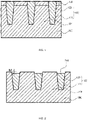
- FIG. 1 to FIG. 9 and FIG. 11 representatively show schematic diagrams of a semiconductor structure in some steps of a manufacturing method of a semiconductor structure proposed by the present disclosure.
- the manufacturing method of a semiconductor structure proposed by the present disclosure is described by taking its application to a semiconductor structure such as DRAM as an example. It is understandable for those skilled in the art that, in order to apply the relevant design of the present disclosure to other types of semiconductor structures or other processes, various modifications, additions, substitutions deletions or other changes may be made to the following specific embodiments, but such changes are still within the scope of the principle of the manufacturing method of a semiconductor structure proposed by the present disclosure.
- the manufacturing method of a semiconductor structure proposed by the present disclosure includes:
- the present disclosure can make the mask thickness of the active regions 101 thinner than that of the isolation regions 102, such that the width of the word line trench formed in the isolation region 102 is less than the width of the word line trench formed in the active region 101 in the subsequent process, and the width of a passing word line 702 is less than that of an active word line 701, thereby reducing the impact of the passing word line 702 and the adverse influence of bit flipping.
- FIG. 1 shows a schematic structural diagram of the semiconductor structure in the step of "providing a substrate 100".
- the semiconductor structure in this step includes the substrate 100 (which is a Si substrate) and the isolation layer 120.
- the substrate 100 includes the active regions 101 and the isolation regions 102.
- the isolation region 102 includes the first trench 111 and the isolation layer 120.
- the isolation layer 120 is formed in the first trench 111, and the sacrificial layer 130 is provided on the upper surfaces of the active regions 101.
- the first trench 111 is opened on the upper surface of the sacrificial layer 130, and the upper surface of the isolation layer 120 is flush with the upper surface of the sacrificial layer 130.
- a material of the isolation layer 120 may include SiO 2 .
- a material of the sacrificial layer 130 may include Si 3 N 4 .
- FIG. 2 shows a schematic structural diagram of the semiconductor structure in the step of "forming first grooves 210".
- the semiconductor structure in this step includes the substrate 100 and the remaining isolation layer 120 after partial removal.
- the first grooves 210 are formed at positions of the removed isolation layer 120, and the sacrificial layer 130 is removed at the same time when part of the isolation layer 120 is removed. After part of the isolation layer 120 is removed, the upper surface of the isolation layer 120 is lower than the upper surface of the substrate 100, thereby forming the first grooves 210.
- each of the first grooves 210 is defined by the upper surface of the remaining isolation layer 120 after partial removal, and the sidewalls of each of the first grooves 210 are defined by partial trench wall of each of the first trenches 111 exposed due to the removal process.
- the sacrificial layer 130 and part of the isolation layer 120 may be removed by a dry etching process.
- a depth h1 of the first groove 210 may be 3 nm to 10 nm, such as 3 nm, 5 nm, 8 nm, 10 nm, etc. In other embodiments, the depth h1 of the first groove 210 may also be less than 3 nm or greater 10 nm, such as 2.5 nm, 11 nm, etc, which is not limited by this embodiment.
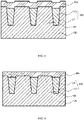
- FIG. 3 shows a schematic structural diagram of the semiconductor structure in the step of "forming first mask layer 300".
- the semiconductor structure in this step includes the substrate 100, the isolation layer 120, and the first mask layer 300.
- the first mask layer 300 covers the upper surfaces of the active regions 101, and the first mask layer 300 fills the first grooves 210.
- the first mask layer 300 also covers the upper surface of the isolation layer 120 and exposed partial sidewalls of each of the first trenches 111.
- a material of the first mask layer 300 may include Si 3 N 4 .
- the first mask layer 300 may be formed by an atomic layer deposition process.
- the thickness of the first mask layer 300 before planarizing is 15 nm to 30 nm, such as 15 nm, 20 nm, 25 nm, 30 nm, etc. In other embodiments, the thickness of the first mask layer 300 before planarizing may also be less than 15 nm or greater than 30 nm, such as 14 nm, 35 nm, etc., which is not limited to this embodiment.
- the depth h1 of the first groove 210 is 3 nm to 10 nm.
- a second thickness h3 of a portion of the first mask layer 300 which covers the active regions 101 is approximately 5 nm to 27 nm
- a first thickness h2 of a portion of the first mask layer 300 which covers the isolation layer 120 still maintains the thickness of the first mask layer 300 before planarizing, that is, 15 nm to 30 nm.
- FIG. 4 shows a schematic structural diagram of the semiconductor structure in the step of "planarizing the first mask layer 300".
- the semiconductor structure in this step includes the substrate 100, the isolation layer 120, and the first mask layer 300 with a planarized upper surface.
- the upper surface of the first mask layer 300 is roughly planar after planarizing. That is, in the first mask layer 300, the upper surface of a portion corresponding to the active regions 101 is flush with the upper surface of a portion corresponding to the isolation regions 102 (the first trenches 111). On this basis, the portion of the first mask layer 300 which corresponds to the isolation regions 102 fills the first trenches 111. Therefore, the first thickness h2 of this portion of the first mask layer 300 is greater than the second thickness h3 of the portion corresponding to the active regions 101.
- the upper surface of the first mask layer 300 may be planarized through a chemical-mechanical polishing (CMP) process.
- CMP chemical-mechanical polishing
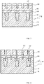
- FIG. 5 to FIG. 9 show schematic structural diagrams of the semiconductor structure in several steps for "forming second trenches 112 and third trenches 113".
- the step of "forming second trenches 112 and third trenches 113" may specifically include:
- the step of forming a patterned photoresist layer 600 on the second mask layer 400 includes:
- a dielectric layer 500 may be formed on the second mask layer 400, where the dielectric layer 500 covers the upper surface of the second mask layer 400.
- the photoresist material layer 601 covers the upper surface of the dielectric layer 500.
- the photoresist material layer 601 may also be formed on the second mask layer 400 by other processes, and can directly cover the upper surface of the second mask layer 400, or spaced by other structures such as the dielectric layer 500 in this embodiment.
- FIG. 5 representatively shows a schematic structural diagram of the semiconductor structure in the step of "forming a photoresist material layer 601".
- the semiconductor structure in this step includes the substrate 100, the isolation layer 120, the first mask layer 300, the second mask layer 400, the dielectric layer 500, and the photoresist material layer 601.
- the second mask layer 400 is formed on the upper surface of the first mask layer 300.
- the dielectric layer 500 is formed on the upper surface of the second mask layer 400.
- the photoresist material layer 601 is coated on the upper surface of the dielectric layer 500.
- FIG. 6 representatively shows a schematic structural diagram of the semiconductor structure in the step of "forming a photoresist layer 600".
- the semiconductor structure in this step includes the substrate 100, the isolation layer 120, the first mask layer 300, the second mask layer 400, the dielectric layer 500, and the pattered photoresist layer 600.
- the second mask layer 400 is formed on the upper surface of the first mask layer 300.
- the dielectric layer 500 is formed on the upper surface of the second mask layer 400.
- the photoresist layer 600 is coated on the upper surface of the dielectric layer 500, and the dielectric layer 500 may be used as an underlying layer in the exposure process.
- the patterned photoresist layer 600 is provided with openings 610.
- the openings 610 correspond to positions of the subsequently formed second trenches 112 and third trenches 113 (i.e., positions of the word line structures) in a one-to-one manner. Widths of the openings 610 are approximately the same.
- a material of the second mask layer 400 may include carbon (C).
- the second mask layer 400 may be formed by a chemical vapor deposition process.
- a thickness of the second mask layer 400 may be 150 nm to 200 nm, such as 150 nm, 160 nm, 175 nm, 200 nm, etc. In other embodiments, the thickness of the second mask layer 400 may also be less than 150 nm or greater than 200 nm, such as 140 nm, 210 nm, and the like, which is not limited in this embodiment.
- a material of the dielectric layer 500 may include Si, Si 3 N 4 or SiON.
- the step of etching part of the first mask layer 300, part of the isolation layer 120, and part of the substrate 100 by using the photoresist layer 600 as a mask includes:
- FIG. 7 shows a schematic structural diagram of the semiconductor structure in the step of "forming fourth trenches 220".
- the semiconductor structure in this step includes the substrate 100, the isolation layer 120, the first mask layer 300, the remaining second mask layer 400 after partial removal, and the remaining dielectric layer 500 after partial removal.
- the patterned photoresist layer 600 as a mask, the patterns of the openings 610 of the photoresist layer 600 are transferred to the dielectric layer 500 and part of the second mask layer 400, and the photoresist layer 600 is completely removed in the exposure process.
- the formed fourth trenches 220 are opened on the upper surface of the dielectric layer 500, and extend to the second mask layer 400.
- FIG. 8 shows a schematic structural diagram of the semiconductor structure in the step of "forming third grooves 230 and fourth grooves 240".
- the semiconductor structure in this step includes the active regions 101, the remaining substrate 100 after partial removal, the remaining isolation layer 120 after partial removal, the remaining first mask layer 300 after partial removal, and the remaining second mask layer 400 after further partial removal.
- the second mask layer 400, the first mask layer 300, the active regions 101, and the isolation layer 120 are continuously etched from the bottom of each of the fourth trenches 220.
- the cross section of each channel formed in the first mask layer 300 in the etching process is in a shape of a trapezoid with a decreasing width from top to bottom.
- the first thickness h2 of the portion of the first mask layer 300 covering the isolation layer 120 is greater than the second thickness h3 of the portion covering the active regions 101. Therefore, an opening width of the channel with the trapezoidal cross section on the upper surface of the active region 101 is greater than its opening width on the upper surface of the isolation layer 120, such that the width of the fourth groove 240 formed, by etching downward from the opening, in the active region 101 is greater than the width of the third groove 230 in the isolation layer 120.
- the third groove 230 is formed under the fourth trench 220 located in the isolation layer 120
- the fourth groove 240 is formed under the fourth trench 220 located in the active region 101.
- FIG. 9 shows a schematic structural diagram of the semiconductor structure in the step of "forming second trenches 112 and third trenches 113"
- FIG. 10 representatively shows a partial enlarged view of the semiconductor structure in FIG. 9 .
- the semiconductor structure in this step includes the active regions 101, the remaining substrate 100 after further partial removal, the remaining isolation layer 120 after further partial removal, and the remaining first mask layer 300 after partial removal.
- the isolation layer 120 is continuously etched from the bottom of each third groove 230 to form the second trench 112, and the active region 101 is continuously etched from the bottom of each fourth groove 240 to form the third trench 113; the second mask layer 400 is completely removed in the foregoing etching process.
- the width of the fourth groove 240 is greater than that of the third groove 230, the third trench 113 is formed by continuously etching from the bottom of the fourth groove 240, and the second trench 112 is formed by continuously etching from the bottom of the third groove 230. Therefore, as shown in FIG. 10 , the first width d1 of the third trench 113 is greater than the second width d2 of the second trench 112.
- a difference between the first width d1 of the third trench 113 and the second width d2 of the second trench 112 may be 1 nm to 5 nm, such as 1 nm, 2 nm, 3.5 nm, 5 nm, etc.
- the difference between the first width d1 of the third trench 113 and the second width d2 of the second trench 112 may also be greater than 5 nm, such as 5.5 nm, which is not limited in this embodiment.
- the depth of the second trench 112 may be 180 nm to 200 nm, such as 180 nm, 190 nm, 195 nm, 200 nm, etc. In other embodiments, the depth of the second trench 112 may also be less than 180 nm or greater than 200 nm, such as 175 nm, 205 nm, etc., which is not limited in this embodiment.
- the depth of the third trench 113 may be 150 nm 170 nm, such 150 nm, 155 nm, 160 nm, 170nm, etc. In other embodiments, the depth of the third trench 113 may also be less than 150 nm or greater than 170 nm, such as 145 nm, 175nm, etc., which is not limited in this embodiment.
- the step of forming word line structures in the second trenches 112 and the third trenches 113 includes:
- the upper surface of the barrier layer 720 is lower than the upper surface of the conductive layer 710.
- GIDL gate-induced drain leakage
- the method further includes: forming a protective layer 800, where the protective layer 800 covers the surface of each of the word line structures and fills the second trenches 112 and the third trenches 113.
- FIG. 11 shows a schematic structural diagram of the semiconductor structure in the step of "forming a metal barrier material layer 721", and specifically shows a partial enlarged view of the semiconductor structure similar to FIG. 10 .
- the semiconductor structure in this step includes the substrate 100, the isolation layer 120, the first mask layer 300, and the metal barrier material layer 721.
- the metal barrier material layer 721 covers the upper surface of the first mask layer 300, and the bottom and sidewalls of each of the second trenches 112 and the third trenches 113.
- FIG. 12 shows a schematic structural diagram of the semiconductor structure in the step of "forming a conductive material layer 711", and specifically shows a partial enlarged view of the semiconductor structure similar to FIG. 10 .
- the semiconductor structure in this step includes the substrate 100, the isolation layer 120, the first mask layer 300, the metal barrier material layer 721, and the conductive material layer 711.
- the conductive material layer 711 covers the surface of the metal barrier material layer, and the conductive material layer 711 fills the second trenches112 and the third trenches 113.
- FIG. 13 shows a schematic structural diagram of the semiconductor structure in the step of "forming word line structures", and specifically shows a partial enlarged view of the semiconductor structure similar to FIG. 10 .
- the semiconductor structure in this step includes the substrate 100, the isolation layer 120, the first mask layer 300, and the word line structures.
- the word line structures are formed in the second trenches 112 and the third trenches 113 respectively. Since the first width d1 of the third trench 113 is greater than the second width d2 of the second trench 112, the word line structure formed in the third trench 113 (i.e., the active word line 701) is greater than the width of the word line structure formed in the second trench 112 (i.e., the passing word line 702).
- each of the word line structures includes the conductive layer 710 and the barrier layer 720; the barrier layer 720 is formed between the conductive layer 710 and the wall of the trench.
- a mask is covered on the substrate, and the mask thickness of the active regions is thinner than that of the isolation regions, such that the width of the word line trench formed in the isolation regions is less than the width of the word line trench formed in the active regions in the subsequent process, and the width of a passing word line is less than that of an active word line, thereby reducing the impact of the passing word line and the adverse influence of bit flipping.
- the applicant conducted experiments.
- the experimental results show that when the depth of the first groove is 5 nm, there will be a width difference of 0.55 nm between the second trench and the third trench, and through numerous experiments, it is concluded the linear relationship between the depth of the first groove and the trench width difference is approximately 0.1 nm of width difference / 1 nm of depth.
- the applicant made the depth of the first groove about 8 nm to 10 nm, and a trench width difference of about 1 nm was generated.
- the semiconductor structure proposed by the present disclosure includes a substrate 100, where the substrate 100 includes active regions 101 and isolation regions 102, each of the isolation regions 102 includes a first trench 111 and an isolation layer 120 formed in the first trenches 111, each of the second trenches 112 is provided on an upper surface of the isolation layer 120, each of the third trenches 113 is provided on an upper surface of each of the active regions 101, a width of the third trench 113 is greater than that of the second trench 112, and word line structures are provided in the third trenches 113 and the second trenches 112 respectively.
- the semiconductor structure further includes a protective layer 800, where the protective layer 800 covers the surfaces of the word line structures and fills the second trenches 112 and the third trenches 113.
- each of the word line structures includes a conductive layer 710 and a barrier layer 720.
- the conductive layer 710 is provided in each of the second trenches 112 and each of the third trenches 113.
- the barrier layer 720 is provided between the conductive layer 710 and the wall of each trench. An upper surface of the barrier layer 720 and an upper surface of the conductive layer 710 are lower than the upper surface of each of the active regions 101.
- a material of the conductive layer 710 may include tungsten (W).
- a material of the barrier layer 720 may include TiN.
- a material of the isolation layer 120 may include SiO 2 .
- a material of the first mask layer 300 may include Si 3 N 4 .
- a first thickness h2 of a portion of the first mask layer 300 which covers the isolation layer 120 may be 15 nm to 30 nm, such as 15 nm, 20 nm, 25 nm, 30 nm, etc. In other embodiments, the first thickness h2 of the portion of the first mask layer 300 which covers the isolation layer 120 may also be less than 15 nm or greater than 30 nm, such as 14 nm, 35 nm, etc., which is not limited in this embodiment.
- a second thickness h3 of a portion of the first mask layer 300 which covers the active regions 101 is approximately 5 nm to 27 nm.
- a difference between a first width d1 of the third trench 113 and a second width d2 of the second trench 112 may be 1 nm to 5 nm, such as 1 nm, 2 nm, 3.5 nm, 5 nm, etc.
- the difference between the first width d1 of the third trench 113 and the second width d2 of the second trench 112 may also be greater than 5 nm, such as 5.5 nm, which is not limited in this embodiment.
- the depth of the second trench 112 may be 180 nm to 200 nm, such as 180 nm, 190 nm, 195 nm, 200 nm, etc. In other embodiments, the depth of the second trench 112 may also be less than 180 nm or greater than 200 nm, such as 175 nm, 205 nm, etc., which is not limited in this embodiment.
- the depth of the third trench 113 may be 150 nm 170 nm, such 150 nm, 155 nm, 160 nm, 170nm, etc. In other embodiments, the depth of the third trench 113 may also be less than 150 nm or greater than 170 nm, such as 145 nm, 175nm, etc., which is not limited in this embodiment.
- the width of the word line trench formed in the isolation regions is less than the width of the word line trench formed in the active regions, and the width of a passing word line is less than that of an active word line, thereby reducing the impact of the passing word line and the adverse influence of bit flipping.
Landscapes
- Element Separation (AREA)
- Drying Of Semiconductors (AREA)
- Semiconductor Memories (AREA)
- Bipolar Transistors (AREA)
- Thin Film Transistor (AREA)
- Liquid Deposition Of Substances Of Which Semiconductor Devices Are Composed (AREA)
Abstract
Description
- The present disclosure claims the priority of
Chinese Patent Application No. 202110291828.7, titled "MANUFACTURING METHOD OF SEMICONDUCTOR STRUCTURE AND SEMICONDUCTOR STRUCTURE", filed on March 18, 2021 - The present disclosure relates to the technical field of semiconductors, and in particular to a manufacturing method of a semiconductor structure and a semiconductor structure.
- There is hardware vulnerability in the existing DRAM semiconductor structure. That is, high frequency access or attacks to a row of data in the memory can cause bit flipping in adjacent rows of data. The vulnerability elevates access permission to the entire memory area. As the manufacturing precision of DRAMs increases, physical space occupied by the components becomes smaller. When a single chip has a large memory capacity, electromagnetic interference between memory cells is unavoidable.
- For a DRAM semiconductor structure, bit flipping is mainly caused by the impact of word lines formed in an adjacent isolation region (i.e., passing word lines) on word lines formed in an active region (i.e., active word lines). In the actual operation of the DRAM, it is the active word lines that really play a role. In order to reduce the effect of bit flipping, the distance between two word line structures can be increased by reducing the width of the passing word line. However, the existing passing word lines and active word lines are formed at the same time, and it is difficult to produce a large size difference through existing processes such as etching.
- According to an aspect, embodiments of the present disclosure provide a manufacturing method of a semiconductor structure, including: providing a substrate, where the substrate includes active regions and isolation regions, each of the isolation regions includes a first trench and an isolation layer formed in the first trench, and a sacrificial layer is provided on the active regions; removing part of the isolation layer to form first grooves; forming a first mask layer, where the first mask layer covers upper surfaces of the active regions and fills the first grooves; planarizing the first mask layer, such that an upper surface of a portion of the first mask layer located above the active regions is flush with an upper surface of a portion of the first mask layer located above the isolation regions; removing part of the first mask layer, part of the isolation layer, and part of the substrate, to form second trenches and third trenches, where each of the second trenches is located in each of the isolation regions, each of the third trenches is located in each of the active regions, and a width of the third trench is greater than a width of the second trench; and forming word line structures in the second trenches and the third trenches.
- According to another aspect, embodiments of the present disclosure provide a semiconductor structure, including: a substrate, second trenches and third trenches, and word line structures, where the substrate includes active regions and isolation regions, each of the isolation regions includes a first trench and an isolation layer formed in the first trench; each of the second trenches is located in each of the isolation regions, each of the third trenches is located in each of the active regions, and a width of the third trench is greater than a width of the second trench; and the word line structures are provided in the second trenches and the third trenches.
-
-
FIG. 1 to FIG. 9 are schematic diagrams of a semiconductor structure in some steps of a manufacturing method proposed by the present disclosure; -
FIG. 10 is a partial enlarged view of the semiconductor structure in the step shown inFIG. 9 ; and -
FIG. 11 to FIG. 14 are schematic diagrams of the semiconductor structure in other steps of the manufacturing method proposed by the present disclosure. - Exemplary embodiments will be described below in further detail with reference to the accompanying drawings. The exemplary embodiments may be implemented in various forms, and may not be construed as being limited to those described herein. On the contrary, these exemplary embodiments are provided to make the present disclosure comprehensive and complete and to fully convey the concept manifested therein to those skilled in the art. The same reference numerals in the figures indicate the same or similar structures, and thus their detailed descriptions will be omitted.
-
FIG. 1 to FIG. 9 andFIG. 11 representatively show schematic diagrams of a semiconductor structure in some steps of a manufacturing method of a semiconductor structure proposed by the present disclosure. In the exemplary embodiment, the manufacturing method of a semiconductor structure proposed by the present disclosure is described by taking its application to a semiconductor structure such as DRAM as an example. It is understandable for those skilled in the art that, in order to apply the relevant design of the present disclosure to other types of semiconductor structures or other processes, various modifications, additions, substitutions deletions or other changes may be made to the following specific embodiments, but such changes are still within the scope of the principle of the manufacturing method of a semiconductor structure proposed by the present disclosure. - As shown in
FIG. 1 to FIG. 13 , in this embodiment, the manufacturing method of a semiconductor structure proposed by the present disclosure includes: - providing a
substrate 100, where thesubstrate 100 includesactive regions 101 andisolation regions 102, each of theisolation regions 102 includes afirst trench 111 and anisolation layer 120 formed in thefirst trench 111, and asacrificial layer 130 is provided on theactive regions 101; - removing part of the
isolation layer 120 to formfirst grooves 210; - forming a
first mask layer 300, where thefirst mask layer 300 covers upper surfaces of theactive regions 101 and fills thefirst grooves 210; - planarizing the
first mask layer 300, such that an upper surface of a portion of thefirst mask layer 300 located above theactive regions 101 is flush with an upper surface of a portion of thefirst mask layer 300 located above theisolation regions 102; - removing part of the
first mask layer 300, part of theisolation layer 120, and part of thesubstrate 100, to formsecond trenches 112 andthird trenches 113, where each of thesecond trenches 112 is located in each of theisolation regions 102, each of thethird trench 113 is located in each of theactive regions 101, and a width of thethird trench 113 is greater than a width of thesecond trench 112; and - forming word line structures in the
second trenches 112 and thethird trenches 113. - Through the design above, the present disclosure can make the mask thickness of the
active regions 101 thinner than that of theisolation regions 102, such that the width of the word line trench formed in theisolation region 102 is less than the width of the word line trench formed in theactive region 101 in the subsequent process, and the width of apassing word line 702 is less than that of anactive word line 701, thereby reducing the impact of thepassing word line 702 and the adverse influence of bit flipping. -
FIG. 1 shows a schematic structural diagram of the semiconductor structure in the step of "providing asubstrate 100". Specifically, the semiconductor structure in this step includes the substrate 100 (which is a Si substrate) and theisolation layer 120. Thesubstrate 100 includes theactive regions 101 and theisolation regions 102. Theisolation region 102 includes thefirst trench 111 and theisolation layer 120. Theisolation layer 120 is formed in thefirst trench 111, and thesacrificial layer 130 is provided on the upper surfaces of theactive regions 101. On this basis, thefirst trench 111 is opened on the upper surface of thesacrificial layer 130, and the upper surface of theisolation layer 120 is flush with the upper surface of thesacrificial layer 130. - Optionally, in the step of "providing a
substrate 100", in this embodiment, a material of theisolation layer 120 may include SiO2. - Optionally, in the step of "providing a
substrate 100", in this embodiment, a material of thesacrificial layer 130 may include Si3N4. -
FIG. 2 shows a schematic structural diagram of the semiconductor structure in the step of "formingfirst grooves 210". Specifically, the semiconductor structure in this step includes thesubstrate 100 and theremaining isolation layer 120 after partial removal. Thefirst grooves 210 are formed at positions of the removedisolation layer 120, and thesacrificial layer 130 is removed at the same time when part of theisolation layer 120 is removed. After part of theisolation layer 120 is removed, the upper surface of theisolation layer 120 is lower than the upper surface of thesubstrate 100, thereby forming thefirst grooves 210. That is, the bottom wall of each of thefirst grooves 210 is defined by the upper surface of theremaining isolation layer 120 after partial removal, and the sidewalls of each of thefirst grooves 210 are defined by partial trench wall of each of thefirst trenches 111 exposed due to the removal process. - Optionally, as shown in
FIG. 2 , in the step of "formingfirst grooves 210", in this embodiment, thesacrificial layer 130 and part of theisolation layer 120 may be removed by a dry etching process. - Optionally, as shown in
FIG. 2 , in the step of "formingfirst grooves 210", in this embodiment, a depth h1 of thefirst groove 210 may be 3 nm to 10 nm, such as 3 nm, 5 nm, 8 nm, 10 nm, etc. In other embodiments, the depth h1 of thefirst groove 210 may also be less than 3 nm or greater 10 nm, such as 2.5 nm, 11 nm, etc, which is not limited by this embodiment. -
FIG. 3 shows a schematic structural diagram of the semiconductor structure in the step of "formingfirst mask layer 300". Specifically, the semiconductor structure in this step includes thesubstrate 100, theisolation layer 120, and thefirst mask layer 300. Thefirst mask layer 300 covers the upper surfaces of theactive regions 101, and thefirst mask layer 300 fills thefirst grooves 210. In other words, thefirst mask layer 300 also covers the upper surface of theisolation layer 120 and exposed partial sidewalls of each of thefirst trenches 111. - Optionally, as shown in
FIG. 3 , in the step of "forming afirst mask layer 300", in this embodiment, a material of thefirst mask layer 300 may include Si3N4. - Optionally, as shown in
FIG. 3 , in the step of "forming afirst mask layer 300", in this embodiment, thefirst mask layer 300 may be formed by an atomic layer deposition process. - Optionally, as shown in
FIG. 3 and FIG. 4 , in the step of "forming afirst mask layer 300", in this embodiment, the thickness of thefirst mask layer 300 before planarizing is 15 nm to 30 nm, such as 15 nm, 20 nm, 25 nm, 30 nm, etc. In other embodiments, the thickness of thefirst mask layer 300 before planarizing may also be less than 15 nm or greater than 30 nm, such as 14 nm, 35 nm, etc., which is not limited to this embodiment. In addition, the depth h1 of thefirst groove 210 is 3 nm to 10 nm. Taking the thickness of thefirst mask layer 300 before planarizing being 15 nm to 30 nm as an example, after thefirst mask layer 300 is planarized, a second thickness h3 of a portion of thefirst mask layer 300 which covers theactive regions 101 is approximately 5 nm to 27 nm, and a first thickness h2 of a portion of thefirst mask layer 300 which covers theisolation layer 120 still maintains the thickness of thefirst mask layer 300 before planarizing, that is, 15 nm to 30 nm. -
FIG. 4 shows a schematic structural diagram of the semiconductor structure in the step of "planarizing thefirst mask layer 300". Specifically, the semiconductor structure in this step includes thesubstrate 100, theisolation layer 120, and thefirst mask layer 300 with a planarized upper surface. The upper surface of thefirst mask layer 300 is roughly planar after planarizing. That is, in thefirst mask layer 300, the upper surface of a portion corresponding to theactive regions 101 is flush with the upper surface of a portion corresponding to the isolation regions 102 (the first trenches 111). On this basis, the portion of thefirst mask layer 300 which corresponds to theisolation regions 102 fills thefirst trenches 111. Therefore, the first thickness h2 of this portion of thefirst mask layer 300 is greater than the second thickness h3 of the portion corresponding to theactive regions 101. - Optionally, as shown in
FIG. 4 , in the step of "planarizing thefirst mask layer 300", in this embodiment, the upper surface of thefirst mask layer 300 may be planarized through a chemical-mechanical polishing (CMP) process. -
FIG. 5 to FIG. 9 show schematic structural diagrams of the semiconductor structure in several steps for "formingsecond trenches 112 andthird trenches 113". Specifically, the step of "formingsecond trenches 112 andthird trenches 113" may specifically include: - forming a
second mask layer 400 on thefirst mask layer 300, where thesecond mask layer 400 covers the surface of thefirst mask layer 300; - forming a
patterned photoresist layer 600 on thesecond mask layer 400; and - etching part of the
first mask layer 300, part of theisolation layer 120, and part of thesubstrate 100 by using thephotoresist layer 600 as a mask. - Further, in this embodiment, the step of forming a
patterned photoresist layer 600 on thesecond mask layer 400 includes: - forming a photoresist material layer on the second mask layer; and
- as shown in
FIG. 6 , removing part of thephotoresist material layer 601 by using an exposure and development technology, where the remainingphotoresist material layer 601 forms thephotoresist layer 600. - Further, as shown in
FIG. 5 and FIG. 6 , in this embodiment, adielectric layer 500 may be formed on thesecond mask layer 400, where thedielectric layer 500 covers the upper surface of thesecond mask layer 400. On this basis, in the step of "forming aphotoresist material layer 601", thephotoresist material layer 601 covers the upper surface of thedielectric layer 500. In other embodiments, thephotoresist material layer 601 may also be formed on thesecond mask layer 400 by other processes, and can directly cover the upper surface of thesecond mask layer 400, or spaced by other structures such as thedielectric layer 500 in this embodiment. -
FIG. 5 representatively shows a schematic structural diagram of the semiconductor structure in the step of "forming aphotoresist material layer 601". Specifically, the semiconductor structure in this step includes thesubstrate 100, theisolation layer 120, thefirst mask layer 300, thesecond mask layer 400, thedielectric layer 500, and thephotoresist material layer 601. Thesecond mask layer 400 is formed on the upper surface of thefirst mask layer 300. Thedielectric layer 500 is formed on the upper surface of thesecond mask layer 400. Thephotoresist material layer 601 is coated on the upper surface of thedielectric layer 500. -
FIG. 6 representatively shows a schematic structural diagram of the semiconductor structure in the step of "forming aphotoresist layer 600". Specifically, the semiconductor structure in this step includes thesubstrate 100, theisolation layer 120, thefirst mask layer 300, thesecond mask layer 400, thedielectric layer 500, and the patteredphotoresist layer 600. Thesecond mask layer 400 is formed on the upper surface of thefirst mask layer 300. Thedielectric layer 500 is formed on the upper surface of thesecond mask layer 400. Thephotoresist layer 600 is coated on the upper surface of thedielectric layer 500, and thedielectric layer 500 may be used as an underlying layer in the exposure process. The patternedphotoresist layer 600 is provided withopenings 610. Theopenings 610 correspond to positions of the subsequently formedsecond trenches 112 and third trenches 113 (i.e., positions of the word line structures) in a one-to-one manner. Widths of theopenings 610 are approximately the same. - Optionally, as shown in
FIG. 5 , in the step of "forming asecond mask layer 400", in this embodiment, a material of thesecond mask layer 400 may include carbon (C). - Optionally, as shown in
FIG. 5 , in the step of "forming asecond mask layer 400", in this embodiment, thesecond mask layer 400 may be formed by a chemical vapor deposition process. - Optionally, as shown in
FIG. 5 , in the step of "forming asecond mask layer 400", in this embodiment, a thickness of thesecond mask layer 400 may be 150 nm to 200 nm, such as 150 nm, 160 nm, 175 nm, 200 nm, etc. In other embodiments, the thickness of thesecond mask layer 400 may also be less than 150 nm or greater than 200 nm, such as 140 nm, 210 nm, and the like, which is not limited in this embodiment. - Optionally, as shown in
FIG. 5 , in the step of "forming adielectric layer 500", in this embodiment, a material of thedielectric layer 500 may include Si, Si3N4 or SiON. - Further, as shown in
FIG. 7 to FIG. 9 , in this embodiment, the step of etching part of thefirst mask layer 300, part of theisolation layer 120, and part of thesubstrate 100 by using thephotoresist layer 600 as a mask includes: - etching part of the
second mask layer 400 by using thephotoresist layer 600 as a mask, to formfourth trenches 220 in thesecond mask layer 400; - removing the
photoresist layer 600; - etching part of the
first mask layer 300, part of theisolation layer 120, and part of thesubstrate 100 downward along thefourth trenches 220; and - removing the
second mask layer 400. -
FIG. 7 shows a schematic structural diagram of the semiconductor structure in the step of "formingfourth trenches 220". Specifically, the semiconductor structure in this step includes thesubstrate 100, theisolation layer 120, thefirst mask layer 300, the remainingsecond mask layer 400 after partial removal, and the remainingdielectric layer 500 after partial removal. By using the patternedphotoresist layer 600 as a mask, the patterns of theopenings 610 of thephotoresist layer 600 are transferred to thedielectric layer 500 and part of thesecond mask layer 400, and thephotoresist layer 600 is completely removed in the exposure process. The formedfourth trenches 220 are opened on the upper surface of thedielectric layer 500, and extend to thesecond mask layer 400. -
FIG. 8 shows a schematic structural diagram of the semiconductor structure in the step of "formingthird grooves 230 andfourth grooves 240". Specifically, the semiconductor structure in this step includes theactive regions 101, the remainingsubstrate 100 after partial removal, the remainingisolation layer 120 after partial removal, the remainingfirst mask layer 300 after partial removal, and the remainingsecond mask layer 400 after further partial removal. Thesecond mask layer 400, thefirst mask layer 300, theactive regions 101, and theisolation layer 120 are continuously etched from the bottom of each of thefourth trenches 220. Moreover, by using a spacing multiplication process, the cross section of each channel formed in thefirst mask layer 300 in the etching process is in a shape of a trapezoid with a decreasing width from top to bottom. The first thickness h2 of the portion of thefirst mask layer 300 covering the isolation layer 120 (i.e., the portion filling the first grooves 210) is greater than the second thickness h3 of the portion covering theactive regions 101. Therefore, an opening width of the channel with the trapezoidal cross section on the upper surface of theactive region 101 is greater than its opening width on the upper surface of theisolation layer 120, such that the width of thefourth groove 240 formed, by etching downward from the opening, in theactive region 101 is greater than the width of thethird groove 230 in theisolation layer 120. In other words, thethird groove 230 is formed under thefourth trench 220 located in theisolation layer 120, and thefourth groove 240 is formed under thefourth trench 220 located in theactive region 101. - As shown in
FIG. 9 and FIG. 10, FIG. 9 shows a schematic structural diagram of the semiconductor structure in the step of "formingsecond trenches 112 andthird trenches 113", andFIG. 10 representatively shows a partial enlarged view of the semiconductor structure inFIG. 9 . Specifically, the semiconductor structure in this step includes theactive regions 101, the remainingsubstrate 100 after further partial removal, the remainingisolation layer 120 after further partial removal, and the remainingfirst mask layer 300 after partial removal. Theisolation layer 120 is continuously etched from the bottom of eachthird groove 230 to form thesecond trench 112, and theactive region 101 is continuously etched from the bottom of eachfourth groove 240 to form thethird trench 113; thesecond mask layer 400 is completely removed in the foregoing etching process. The width of thefourth groove 240 is greater than that of thethird groove 230, thethird trench 113 is formed by continuously etching from the bottom of thefourth groove 240, and thesecond trench 112 is formed by continuously etching from the bottom of thethird groove 230. Therefore, as shown inFIG. 10 , the first width d1 of thethird trench 113 is greater than the second width d2 of thesecond trench 112. - Optionally, as shown in
FIG. 10 , in the step of "formingsecond trenches 112 andthird trenches 113", in this embodiment, a difference between the first width d1 of thethird trench 113 and the second width d2 of thesecond trench 112 may be 1 nm to 5 nm, such as 1 nm, 2 nm, 3.5 nm, 5 nm, etc. In other embodiments, the difference between the first width d1 of thethird trench 113 and the second width d2 of thesecond trench 112 may also be greater than 5 nm, such as 5.5 nm, which is not limited in this embodiment. - Optionally, as shown in
FIG. 10 , in the step of "formingsecond trenches 112 andthird trenches 113", in this embodiment, the depth of thesecond trench 112 may be 180 nm to 200 nm, such as 180 nm, 190 nm, 195 nm, 200 nm, etc. In other embodiments, the depth of thesecond trench 112 may also be less than 180 nm or greater than 200 nm, such as 175 nm, 205 nm, etc., which is not limited in this embodiment. - Optionally, as shown in
FIG. 10 , in the step of "formingsecond trenches 112 andthird trenches 113", in this embodiment, the depth of thethird trench 113 may be 150 nm 170 nm, such 150 nm, 155 nm, 160 nm, 170nm, etc. In other embodiments, the depth of thethird trench 113 may also be less than 150 nm or greater than 170 nm, such as 145 nm, 175nm, etc., which is not limited in this embodiment. - Optionally, in this embodiment, the step of forming word line structures in the
second trenches 112 and thethird trenches 113 includes: - as shown in
FIG. 11 , forming a metalbarrier material layer 721, where the metalbarrier material layer 721 covers the upper surface of thefirst mask layer 300, and the bottom and sidewalls of each of thesecond trenches 112 and thethird trenches 113; - as shown in
FIG. 12 , forming aconductive material layer 711, where theconductive material layer 711 covers the surface of the metal barrier material layer, and theconductive material layer 711 fills thesecond trenches 112 and thethird trenches 113; and - as shown in
FIG. 13 , removing part of the metalbarrier material layer 721 and part of theconductive material layer 721, where the remaining metalbarrier material layer 721 is abarrier layer 720, and the remainingconductive material layer 711 is aconductive layer 710, thebarrier layer 720 and theconductive layer 710 forming each of the word line structures; - where an upper surface of the
barrier layer 720 and an upper surface of theconductive layer 710 are lower than the upper surface of each of theactive regions 101. - Further, in the step of "forming the word line structures", in this embodiment, the upper surface of the
barrier layer 720 is lower than the upper surface of theconductive layer 710. Thus, a gate-induced drain leakage (GIDL) can be reduced. - Further, in the step of "forming the word line structures", in this embodiment, after the step of forming word line structures in the
second trenches 112 and thethird trenches 113, the method further includes:
forming aprotective layer 800, where theprotective layer 800 covers the surface of each of the word line structures and fills thesecond trenches 112 and thethird trenches 113. -
FIG. 11 shows a schematic structural diagram of the semiconductor structure in the step of "forming a metalbarrier material layer 721", and specifically shows a partial enlarged view of the semiconductor structure similar toFIG. 10 . Specifically, the semiconductor structure in this step includes thesubstrate 100, theisolation layer 120, thefirst mask layer 300, and the metalbarrier material layer 721. The metalbarrier material layer 721 covers the upper surface of thefirst mask layer 300, and the bottom and sidewalls of each of thesecond trenches 112 and thethird trenches 113. -
FIG. 12 shows a schematic structural diagram of the semiconductor structure in the step of "forming aconductive material layer 711", and specifically shows a partial enlarged view of the semiconductor structure similar toFIG. 10 . Specifically, the semiconductor structure in this step includes thesubstrate 100, theisolation layer 120, thefirst mask layer 300, the metalbarrier material layer 721, and theconductive material layer 711. Theconductive material layer 711 covers the surface of the metal barrier material layer, and theconductive material layer 711 fills the second trenches112 and thethird trenches 113. -
FIG. 13 shows a schematic structural diagram of the semiconductor structure in the step of "forming word line structures", and specifically shows a partial enlarged view of the semiconductor structure similar toFIG. 10 . Specifically, the semiconductor structure in this step includes thesubstrate 100, theisolation layer 120, thefirst mask layer 300, and the word line structures. The word line structures are formed in thesecond trenches 112 and thethird trenches 113 respectively. Since the first width d1 of thethird trench 113 is greater than the second width d2 of thesecond trench 112, the word line structure formed in the third trench 113 (i.e., the active word line 701) is greater than the width of the word line structure formed in the second trench 112 (i.e., the passing word line 702). In addition, each of the word line structures includes theconductive layer 710 and thebarrier layer 720; thebarrier layer 720 is formed between theconductive layer 710 and the wall of the trench. - In summary, in the manufacturing method of a semiconductor structure proposed by the present disclosure, a mask is covered on the substrate, and the mask thickness of the active regions is thinner than that of the isolation regions, such that the width of the word line trench formed in the isolation regions is less than the width of the word line trench formed in the active regions in the subsequent process, and the width of a passing word line is less than that of an active word line, thereby reducing the impact of the passing word line and the adverse influence of bit flipping.
- Moreover, in order to verify the efficacy of the manufacturing method of a semiconductor structure proposed by the present disclosure and the manufactured semiconductor structure, the applicant conducted experiments. The experimental results show that when the depth of the first groove is 5 nm, there will be a width difference of 0.55 nm between the second trench and the third trench, and through numerous experiments, it is concluded the linear relationship between the depth of the first groove and the trench width difference is approximately 0.1 nm of width difference / 1 nm of depth. In the actual production, the applicant made the depth of the first groove about 8 nm to 10 nm, and a trench width difference of about 1 nm was generated.
- Based on the above detailed description of an exemplary embodiment of the manufacturing method of a semiconductor structure proposed by the present disclosure, an exemplary embodiment of the semiconductor structure proposed by the present disclosure is described below with reference to
FIG. 13 . - As shown in
FIG. 13 , in this embodiment, the semiconductor structure proposed by the present disclosure includes asubstrate 100, where thesubstrate 100 includesactive regions 101 andisolation regions 102, each of theisolation regions 102 includes afirst trench 111 and anisolation layer 120 formed in thefirst trenches 111, each of thesecond trenches 112 is provided on an upper surface of theisolation layer 120, each of thethird trenches 113 is provided on an upper surface of each of theactive regions 101, a width of thethird trench 113 is greater than that of thesecond trench 112, and word line structures are provided in thethird trenches 113 and thesecond trenches 112 respectively. - Optionally, as shown in
FIG. 14 , in this embodiment, the semiconductor structure further includes aprotective layer 800, where theprotective layer 800 covers the surfaces of the word line structures and fills thesecond trenches 112 and thethird trenches 113. - Optionally, as shown in
FIG. 13 , in this embodiment, each of the word line structures includes aconductive layer 710 and abarrier layer 720. Theconductive layer 710 is provided in each of thesecond trenches 112 and each of thethird trenches 113. Thebarrier layer 720 is provided between theconductive layer 710 and the wall of each trench. An upper surface of thebarrier layer 720 and an upper surface of theconductive layer 710 are lower than the upper surface of each of theactive regions 101. - Further, based on the design that each word line structure includes the
conductive layer 710, in this embodiment, a material of theconductive layer 710 may include tungsten (W). - Further, based on the design that each word line structure includes the
barrier layer 720, in this embodiment, a material of thebarrier layer 720 may include TiN. - Optionally, as shown in
FIG. 13 , in this embodiment, a material of theisolation layer 120 may include SiO2. - Optionally, as shown in
FIG. 13 , in this embodiment, a material of thefirst mask layer 300 may include Si3N4. - Optionally, as shown in
FIG. 13 , in this embodiment, a first thickness h2 of a portion of thefirst mask layer 300 which covers theisolation layer 120 may be 15 nm to 30 nm, such as 15 nm, 20 nm, 25 nm, 30 nm, etc. In other embodiments, the first thickness h2 of the portion of thefirst mask layer 300 which covers theisolation layer 120 may also be less than 15 nm or greater than 30 nm, such as 14 nm, 35 nm, etc., which is not limited in this embodiment. In addition, taking a depth h1 of thefirst groove 210 being 3 nm to 10 nm and the first thickness h2 of the portion of thefirst mask layer 300 which covers theisolation layer 120 being 15 nm to 30 nm as an example, a second thickness h3 of a portion of thefirst mask layer 300 which covers theactive regions 101 is approximately 5 nm to 27 nm. - Optionally, as shown in
FIG. 13 , in this embodiment, a difference between a first width d1 of thethird trench 113 and a second width d2 of thesecond trench 112 may be 1 nm to 5 nm, such as 1 nm, 2 nm, 3.5 nm, 5 nm, etc. In other embodiments, the difference between the first width d1 of thethird trench 113 and the second width d2 of thesecond trench 112 may also be greater than 5 nm, such as 5.5 nm, which is not limited in this embodiment. - Optionally, as shown in
FIG. 13 , in this embodiment, the depth of thesecond trench 112 may be 180 nm to 200 nm, such as 180 nm, 190 nm, 195 nm, 200 nm, etc. In other embodiments, the depth of thesecond trench 112 may also be less than 180 nm or greater than 200 nm, such as 175 nm, 205 nm, etc., which is not limited in this embodiment. - Optionally, as shown in
FIG. 13 , in this embodiment, the depth of thethird trench 113 may be 150 nm 170 nm, such 150 nm, 155 nm, 160 nm, 170nm, etc. In other embodiments, the depth of thethird trench 113 may also be less than 150 nm or greater than 170 nm, such as 145 nm, 175nm, etc., which is not limited in this embodiment. - In summary, in the semiconductor structure proposed by the present disclosure, the width of the word line trench formed in the isolation regions is less than the width of the word line trench formed in the active regions, and the width of a passing word line is less than that of an active word line, thereby reducing the impact of the passing word line and the adverse influence of bit flipping.
- The present disclosure is described above with reference to several typical implementations. It should be understood that the terms used herein are intended for illustration, rather than limiting. The present disclosure may be specifically implemented in many forms without departing from the spirit or essence of the present disclosure. Therefore, it should be understood that the above embodiments are not limited to any of the above-mentioned details, but should be broadly interpreted according to the spirit and scope defined by the appended claims. Therefore, any changes and modifications falling within the claims or the equivalent scope thereof should be covered by the appended claims.
Claims (19)
- A manufacturing method of a semiconductor structure, comprising:providing a substrate, wherein the substrate comprises active regions and isolation regions, each of the isolation regions comprises a first trench and an isolation layer formed in the first trench, and a sacrificial layer is provided on the active regions;removing part of the isolation layer to form first grooves;forming a first mask layer, wherein the first mask layer covers upper surfaces of the active regions and fills the first grooves;planarizing the first mask layer, such that an upper surface of a portion of the first mask layer located above the active regions is flush with an upper surface of a portion of the first mask layer located above the isolation regions;removing part of the first mask layer, part of the isolation layer, and part of the substrate, to form second trenches and third trenches, wherein each of the second trenches is located in each of the isolation regions, each of the third trenches is located in each of the active regions, and a width of the third trench is greater than a width of the second trench; andforming word line structures in the second trenches and the third trenches.
- The manufacturing method of the semiconductor structure according to claim 1, wherein the second trench has a depth of 180 nm to 200 nm.
- The manufacturing method of the semiconductor structure according to claim 1, wherein the third trench has a depth of 150 nm to 170 nm.
- The manufacturing method of the semiconductor structure according to claim 1, wherein a difference between the width of the third trench and the width of the second trench is 1 nm to 5 nm.
- The manufacturing method of the semiconductor structure according to claim 1, wherein the step of forming the first grooves comprises:
removing the sacrificial layer and part of the isolation layer by an etching process, such that an upper surface of the isolation layer is lower than upper surfaces of the active regions. - The manufacturing method of the semiconductor structure according to claim 1, wherein a material of the first mask layer comprises Si3N4.
- The manufacturing method of the semiconductor structure according to claim 1, wherein the first mask layer has a thickness of 15 nm to 30 nm.
- The manufacturing method of the semiconductor structure according to claim 1, wherein the first mask layer is formed by an atomic layer deposition process.
- The manufacturing method of the semiconductor structure according to claim 1, wherein the step of planarizing the first mask layer comprises:
planarizing the first mask layer by a chemical-mechanical polishing process. - The manufacturing method of the semiconductor structure according to claim 1, wherein the step of removing part of the first mask layer, part of the isolation layer, and part of the substrate, to form second trenches and third trenches comprises:forming a second mask layer on the first mask layer, wherein the second mask layer covers a surface of the first mask layer;forming a patterned photoresist layer on the second mask layer; andetching part of the first mask layer, part of the isolation layer, and part of the substrate by using the photoresist layer as a mask.
- The manufacturing method of the semiconductor structure according to claim 10, wherein the step of forming a patterned photoresist layer on the second mask layer comprises:forming a photoresist material layer on the second mask layer; andremoving part of the photoresist material layer by using an exposure and development technology, wherein the remaining photoresist material layer forms the photoresist layer.
- The manufacturing method of the semiconductor structure according to claim 10, wherein the step of etching part of the first mask layer, part of the isolation layer, and part of the substrate by using the photoresist layer as a mask comprises:etching part of the second mask layer by using the photoresist layer as a mask, to form fourth trenches in the second mask layer;removing the photoresist layer;etching part of the first mask layer, part of the isolation layer, and part of the substrate downward along the fourth trenches; andremoving the second mask layer.
- The manufacturing method of the semiconductor structure according to claim 1, wherein the step of forming word line structures in the second trenches and the third trenches comprises:forming a metal barrier material layer, wherein the metal barrier material layer covers an upper surface of the first mask layer, and a bottom and sidewalls of each of the second trenches and the third trenches;forming a conductive material layer, wherein the conductive material layer covers a surface of the metal barrier material layer and fills the second trenches and the third trenches; andremoving part of the metal barrier material layer and part of the conductive material layer, wherein the remaining metal barrier material layer is a barrier layer, and the remaining conductive material layer is a conductive layer, the barrier layer and the conductive layer forming each of the word line structures;wherein an upper surface of the barrier layer and an upper surface of the conductive layer are lower than upper surface of each of the active regions.
- The manufacturing method of the semiconductor structure according to claim 13, wherein
the upper surface of the barrier layer is lower than the upper surface of the conductive layer. - The manufacturing method of the semiconductor structure according to claim 1, after the step of forming word line structures in the second trenches and the third trenches, the method further comprises:
forming a protective layer, wherein the protective layer covers surfaces of the word line structures and fills the second trenches and the third trenches. - A semiconductor structure, comprising:a substrate, comprising active regions and isolation regions, wherein each of the isolation regions comprises a first trench and an isolation layer formed in the first trench;second trenches and third trenches, wherein each of the second trenches is located in each of the isolation regions, each of the third trenches is located in each of the active regions, and a width of the third trench is greater than a width of the second trench; andword line structures, wherein the word line structures are provided in the second trenches and the third trenches.
- The semiconductor structure according to claim 16, wherein an upper surface of the isolation layer is lower than upper surfaces of the active regions.
- The semiconductor structure according to claim 17, wherein each of the word line structures comprise a barrier layer and a conductive layer, and an upper surface of the barrier layer and an upper surface of the conductive layer are lower than the upper surface of each of the active regions.
- The semiconductor structure according to claim 18, further comprising:
a protective layer, wherein the protective layer covers surfaces of the word line structures and fills the second trenches and the third trenches.
Applications Claiming Priority (2)
| Application Number | Priority Date | Filing Date | Title |
|---|---|---|---|
| CN202110291828.7A CN115116960A (en) | 2021-03-18 | 2021-03-18 | Manufacturing method of semiconductor structure and semiconductor structure |
| PCT/CN2021/111829 WO2022193535A1 (en) | 2021-03-18 | 2021-08-10 | Manufacturing method for semiconductor structure, and semiconductor structure |
Publications (3)
| Publication Number | Publication Date |
|---|---|
| EP4086960A1 true EP4086960A1 (en) | 2022-11-09 |
| EP4086960A4 EP4086960A4 (en) | 2023-08-30 |
| EP4086960B1 EP4086960B1 (en) | 2025-10-01 |
Family
ID=83284220
Family Applications (1)
| Application Number | Title | Priority Date | Filing Date |
|---|---|---|---|
| EP21908076.9A Active EP4086960B1 (en) | 2021-03-18 | 2021-08-10 | Manufacturing method for semiconductor structure, and semiconductor structure |
Country Status (4)
| Country | Link |
|---|---|
| US (1) | US12080758B2 (en) |
| EP (1) | EP4086960B1 (en) |
| JP (1) | JP7457127B2 (en) |
| KR (1) | KR102736795B1 (en) |
Cited By (1)
| Publication number | Priority date | Publication date | Assignee | Title |
|---|---|---|---|---|
| FR3156239A1 (en) * | 2023-12-01 | 2025-06-06 | Stmicroelectronics International N.V. | Method of manufacturing an integrated circuit and corresponding integrated circuit |
Families Citing this family (6)
| Publication number | Priority date | Publication date | Assignee | Title |
|---|---|---|---|---|
| US12170232B2 (en) * | 2021-04-30 | 2024-12-17 | Changxin Memory Technologies, Inc. | Manufacturing method and measurement method of semiconductor structure, andsemiconductor structure |
| US12112950B2 (en) | 2022-02-09 | 2024-10-08 | Nanya Technology Corporation | Semiconductor device with protection layer and method for fabricating the same |
| US20230253210A1 (en) * | 2022-02-09 | 2023-08-10 | Nanya Technology Corporation | Semiconductor device with protection layer |
| CN117320441A (en) * | 2022-06-22 | 2023-12-29 | 长鑫存储技术有限公司 | Semiconductor structures and manufacturing methods |
| US12482748B2 (en) * | 2023-04-11 | 2025-11-25 | Nanya Technology Corporation | Method of manufacturing semiconductor structure including nitrogen treatment and semiconductor structure thereof |
| CN118553605B (en) * | 2024-07-24 | 2024-10-22 | 杭州积海半导体有限公司 | A mask layer and a method for forming the same |
Family Cites Families (25)
| Publication number | Priority date | Publication date | Assignee | Title |
|---|---|---|---|---|
| DE10312469A1 (en) * | 2003-03-20 | 2004-10-07 | Infineon Technologies Ag | Method of manufacturing a semiconductor structure |
| KR20070002118A (en) | 2005-06-30 | 2007-01-05 | 삼성전자주식회사 | Method of manufacturing semiconductor device having gate structure with increased channel length and width |
| KR100825796B1 (en) | 2006-12-14 | 2008-04-28 | 삼성전자주식회사 | Method for manufacturing semiconductor device with buried gate |
| KR20090044855A (en) * | 2007-11-01 | 2009-05-07 | 주식회사 하이닉스반도체 | Manufacturing method of semiconductor device |
| TW200924109A (en) * | 2007-11-21 | 2009-06-01 | Promos Technologies Inc | Method for forming shallow trench isolation structure and method for preparing recessed gate structure using the same |
| KR20090068714A (en) | 2007-12-24 | 2009-06-29 | 주식회사 하이닉스반도체 | Method of manufacturing transistor of semiconductor device |
| KR101078726B1 (en) | 2009-02-27 | 2011-11-01 | 주식회사 하이닉스반도체 | Semiconductor device and method of manufacturing the same |
| KR101061321B1 (en) * | 2009-03-02 | 2011-08-31 | 주식회사 하이닉스반도체 | Saddle pin transistor with raised landing plug contact and its formation method |
| KR101060611B1 (en) * | 2009-07-03 | 2011-08-31 | 주식회사 하이닉스반도체 | Method of manufacturing semiconductor device with buried gate |
| KR101150552B1 (en) * | 2009-12-04 | 2012-06-01 | 에스케이하이닉스 주식회사 | Semiconductor device and method for forming using the same |
| JP2012134395A (en) | 2010-12-22 | 2012-07-12 | Elpida Memory Inc | Semiconductor device and semiconductor device manufacturing method |
| KR101979901B1 (en) * | 2012-12-05 | 2019-08-28 | 삼성전자주식회사 | Method for fabricating a semiconductor device |
| KR101966277B1 (en) | 2013-07-31 | 2019-08-13 | 에스케이하이닉스 주식회사 | Seminconductor having passing gate and method of the same |
| CN104425278B (en) | 2013-09-04 | 2018-12-21 | 中芯国际集成电路制造(上海)有限公司 | The forming method of semiconductor devices and semiconductor devices |
| KR20150044616A (en) * | 2013-10-17 | 2015-04-27 | 삼성전자주식회사 | Method of manufacturing a semiconductor device |
| KR102444838B1 (en) * | 2015-06-30 | 2022-09-22 | 에스케이하이닉스 주식회사 | Semiconductor device with air gap and method for manufacturing the same |
| US20180130702A1 (en) * | 2016-11-08 | 2018-05-10 | Globalfoundries Inc. | Encapsulation of cobalt metallization |
| CN108305876A (en) | 2017-01-11 | 2018-07-20 | 联华电子股份有限公司 | Semiconductor device and method for fabricating the same |
| KR102358460B1 (en) * | 2017-08-10 | 2022-02-07 | 삼성전자주식회사 | Semiconductor memory device and method of forming the same |
| KR102342551B1 (en) * | 2017-09-25 | 2021-12-23 | 삼성전자주식회사 | Semiconductor device including isolation region |
| CN110534480B (en) | 2018-05-25 | 2024-05-07 | 长鑫存储技术有限公司 | Semiconductor memory structure and word line manufacturing method thereof |
| CN110896076B (en) | 2018-09-13 | 2024-12-10 | 长鑫存储技术有限公司 | Semiconductor device and method for manufacturing the same |
| KR102697920B1 (en) * | 2018-11-26 | 2024-08-22 | 삼성전자주식회사 | Semiconductor device and method of fabricating the same |
| CN112447605B (en) | 2019-08-30 | 2025-01-21 | 长鑫存储技术有限公司 | DRAM memory and method of forming the same |
| US11264391B1 (en) * | 2020-10-15 | 2022-03-01 | Nanya Technology Corporation | Semiconductor structure and manufacturing method thereof |
-
2021
- 2021-08-10 EP EP21908076.9A patent/EP4086960B1/en active Active
- 2021-08-10 JP JP2022541010A patent/JP7457127B2/en active Active
- 2021-08-10 KR KR1020227022483A patent/KR102736795B1/en active Active
- 2021-11-15 US US17/454,871 patent/US12080758B2/en active Active
Cited By (1)
| Publication number | Priority date | Publication date | Assignee | Title |
|---|---|---|---|---|
| FR3156239A1 (en) * | 2023-12-01 | 2025-06-06 | Stmicroelectronics International N.V. | Method of manufacturing an integrated circuit and corresponding integrated circuit |
Also Published As
| Publication number | Publication date |
|---|---|
| US20220302253A1 (en) | 2022-09-22 |
| EP4086960B1 (en) | 2025-10-01 |
| KR102736795B1 (en) | 2024-11-29 |
| EP4086960A4 (en) | 2023-08-30 |
| US12080758B2 (en) | 2024-09-03 |
| JP7457127B2 (en) | 2024-03-27 |
| KR20220131227A (en) | 2022-09-27 |
| JP2023522524A (en) | 2023-05-31 |
Similar Documents
| Publication | Publication Date | Title |
|---|---|---|
| EP4086960B1 (en) | Manufacturing method for semiconductor structure, and semiconductor structure | |
| US9613967B1 (en) | Memory device and method of fabricating the same | |
| JP4233953B2 (en) | Method for fabricating a composite integrated circuit including a vertical dynamic random access memory (DRAM) array and a logic circuit portion | |
| US9048293B2 (en) | Semiconductor device and method for manufacturing the same | |
| US11887859B2 (en) | Method for forming active region array and semiconductor structure | |
| US20200152639A1 (en) | Semiconductor structure and manufacturing method thereof | |
| EP4475183B1 (en) | Semiconductor structure and method for forming same | |
| CN112447603B (en) | Method of forming semiconductor memory | |
| KR101150586B1 (en) | Method for forming semiconductor device | |
| TWI906148B (en) | Memory structure | |
| TWI905992B (en) | Memory structure | |
| KR20130106110A (en) | Semiconductor device having isolation region | |
| WO2022193535A1 (en) | Manufacturing method for semiconductor structure, and semiconductor structure | |
| TW201635490A (en) | Semiconductor component with buried word line | |
| US11264391B1 (en) | Semiconductor structure and manufacturing method thereof | |
| EP4036960B1 (en) | Memory forming method and memory | |
| CN114005791A (en) | Memory device and method of forming the same | |
| US9263321B2 (en) | Semiconductor device and manufacturing method thereof | |
| WO2023231196A1 (en) | Semiconductor structure and method for forming same | |
| US8053370B2 (en) | Semiconductor device and fabrications thereof | |
| EP4318549B1 (en) | Semiconductor structure and forming method therefor | |
| US11374009B2 (en) | Integrated circuit device and manufacturing method thereof | |
| CN115000150A (en) | Semiconductor device, electronic apparatus and manufacturing method | |
| US9059194B2 (en) | High-K and metal filled trench-type EDRAM capacitor with electrode depth and dimension control | |
| US20230253255A1 (en) | Manufacturing method for semiconductor structure and semiconductor structure |
Legal Events
| Date | Code | Title | Description |
|---|---|---|---|
| STAA | Information on the status of an ep patent application or granted ep patent |
Free format text: STATUS: UNKNOWN |
|
| STAA | Information on the status of an ep patent application or granted ep patent |
Free format text: STATUS: THE INTERNATIONAL PUBLICATION HAS BEEN MADE |
|
| PUAI | Public reference made under article 153(3) epc to a published international application that has entered the european phase |
Free format text: ORIGINAL CODE: 0009012 |
|
| STAA | Information on the status of an ep patent application or granted ep patent |
Free format text: STATUS: REQUEST FOR EXAMINATION WAS MADE |
|
| 17P | Request for examination filed |
Effective date: 20220628 |
|
| AK | Designated contracting states |
Kind code of ref document: A1 Designated state(s): AL AT BE BG CH CY CZ DE DK EE ES FI FR GB GR HR HU IE IS IT LI LT LU LV MC MK MT NL NO PL PT RO RS SE SI SK SM TR |
|
| REG | Reference to a national code |
Ref country code: DE Ref legal event code: R079 Free format text: PREVIOUS MAIN CLASS: H01L0027108000 Ipc: H10B0012000000 Ref country code: DE Ref legal event code: R079 Ref document number: 602021039826 Country of ref document: DE Free format text: PREVIOUS MAIN CLASS: H01L0027108000 Ipc: H10B0012000000 |
|
| A4 | Supplementary search report drawn up and despatched |
Effective date: 20230726 |
|
| RIC1 | Information provided on ipc code assigned before grant |
Ipc: H01L 21/033 20060101ALI20230721BHEP Ipc: H01L 21/28 20060101ALI20230721BHEP Ipc: H01L 29/423 20060101ALI20230721BHEP Ipc: H01L 21/321 20060101ALI20230721BHEP Ipc: H01L 21/308 20060101ALI20230721BHEP Ipc: H10B 12/00 20230101AFI20230721BHEP |
|
| DAV | Request for validation of the european patent (deleted) | ||
| DAX | Request for extension of the european patent (deleted) | ||
| GRAP | Despatch of communication of intention to grant a patent |
Free format text: ORIGINAL CODE: EPIDOSNIGR1 |
|
| STAA | Information on the status of an ep patent application or granted ep patent |
Free format text: STATUS: GRANT OF PATENT IS INTENDED |
|
| RIC1 | Information provided on ipc code assigned before grant |
Ipc: H10B 12/00 20230101AFI20250708BHEP Ipc: H01L 21/308 20060101ALI20250708BHEP Ipc: H01L 21/321 20060101ALI20250708BHEP Ipc: H10D 64/27 20250101ALI20250708BHEP Ipc: H01L 21/28 20060101ALI20250708BHEP Ipc: H01L 21/033 20060101ALI20250708BHEP |
|
| GRAS | Grant fee paid |
Free format text: ORIGINAL CODE: EPIDOSNIGR3 |
|
| INTG | Intention to grant announced |
Effective date: 20250725 |
|
| GRAA | (expected) grant |
Free format text: ORIGINAL CODE: 0009210 |
|
| STAA | Information on the status of an ep patent application or granted ep patent |
Free format text: STATUS: THE PATENT HAS BEEN GRANTED |
|
| P01 | Opt-out of the competence of the unified patent court (upc) registered |
Free format text: CASE NUMBER: UPC_APP_3324_4086960/2025 Effective date: 20250814 |
|
| AK | Designated contracting states |
Kind code of ref document: B1 Designated state(s): AL AT BE BG CH CY CZ DE DK EE ES FI FR GB GR HR HU IE IS IT LI LT LU LV MC MK MT NL NO PL PT RO RS SE SI SK SM TR |
|
| REG | Reference to a national code |
Ref country code: GB Ref legal event code: FG4D Ref country code: CH Ref legal event code: F10 Free format text: ST27 STATUS EVENT CODE: U-0-0-F10-F00 (AS PROVIDED BY THE NATIONAL OFFICE) Effective date: 20251001 |
|
| REG | Reference to a national code |
Ref country code: DE Ref legal event code: R096 Ref document number: 602021039826 Country of ref document: DE |
|
| REG | Reference to a national code |
Ref country code: IE Ref legal event code: FG4D |
|
| REG | Reference to a national code |
Ref country code: NL Ref legal event code: MP Effective date: 20251001 |
|
| REG | Reference to a national code |
Ref country code: AT Ref legal event code: MK05 Ref document number: 1844001 Country of ref document: AT Kind code of ref document: T Effective date: 20251001 |
|
| PG25 | Lapsed in a contracting state [announced via postgrant information from national office to epo] |
Ref country code: NL Free format text: LAPSE BECAUSE OF FAILURE TO SUBMIT A TRANSLATION OF THE DESCRIPTION OR TO PAY THE FEE WITHIN THE PRESCRIBED TIME-LIMIT Effective date: 20251001 |
|
| PG25 | Lapsed in a contracting state [announced via postgrant information from national office to epo] |
Ref country code: ES Free format text: LAPSE BECAUSE OF FAILURE TO SUBMIT A TRANSLATION OF THE DESCRIPTION OR TO PAY THE FEE WITHIN THE PRESCRIBED TIME-LIMIT Effective date: 20251001 |
|
| REG | Reference to a national code |
Ref country code: LT Ref legal event code: MG9D |
|
| PG25 | Lapsed in a contracting state [announced via postgrant information from national office to epo] |
Ref country code: NO Free format text: LAPSE BECAUSE OF FAILURE TO SUBMIT A TRANSLATION OF THE DESCRIPTION OR TO PAY THE FEE WITHIN THE PRESCRIBED TIME-LIMIT Effective date: 20260101 |
|
| PG25 | Lapsed in a contracting state [announced via postgrant information from national office to epo] |
Ref country code: HR Free format text: LAPSE BECAUSE OF FAILURE TO SUBMIT A TRANSLATION OF THE DESCRIPTION OR TO PAY THE FEE WITHIN THE PRESCRIBED TIME-LIMIT Effective date: 20251001 Ref country code: FI Free format text: LAPSE BECAUSE OF FAILURE TO SUBMIT A TRANSLATION OF THE DESCRIPTION OR TO PAY THE FEE WITHIN THE PRESCRIBED TIME-LIMIT Effective date: 20251001 Ref country code: AT Free format text: LAPSE BECAUSE OF FAILURE TO SUBMIT A TRANSLATION OF THE DESCRIPTION OR TO PAY THE FEE WITHIN THE PRESCRIBED TIME-LIMIT Effective date: 20251001 |
|
| PG25 | Lapsed in a contracting state [announced via postgrant information from national office to epo] |
Ref country code: RS Free format text: LAPSE BECAUSE OF FAILURE TO SUBMIT A TRANSLATION OF THE DESCRIPTION OR TO PAY THE FEE WITHIN THE PRESCRIBED TIME-LIMIT Effective date: 20260101 |
|
| PG25 | Lapsed in a contracting state [announced via postgrant information from national office to epo] |
Ref country code: IS Free format text: LAPSE BECAUSE OF FAILURE TO SUBMIT A TRANSLATION OF THE DESCRIPTION OR TO PAY THE FEE WITHIN THE PRESCRIBED TIME-LIMIT Effective date: 20260201 |
|
| PG25 | Lapsed in a contracting state [announced via postgrant information from national office to epo] |
Ref country code: CZ Free format text: LAPSE BECAUSE OF FAILURE TO SUBMIT A TRANSLATION OF THE DESCRIPTION OR TO PAY THE FEE WITHIN THE PRESCRIBED TIME-LIMIT Effective date: 20251001 Ref country code: PT Free format text: LAPSE BECAUSE OF FAILURE TO SUBMIT A TRANSLATION OF THE DESCRIPTION OR TO PAY THE FEE WITHIN THE PRESCRIBED TIME-LIMIT Effective date: 20260202 |
|
| PG25 | Lapsed in a contracting state [announced via postgrant information from national office to epo] |
Ref country code: PL Free format text: LAPSE BECAUSE OF FAILURE TO SUBMIT A TRANSLATION OF THE DESCRIPTION OR TO PAY THE FEE WITHIN THE PRESCRIBED TIME-LIMIT Effective date: 20251001 |
|
| PG25 | Lapsed in a contracting state [announced via postgrant information from national office to epo] |
Ref country code: LV Free format text: LAPSE BECAUSE OF FAILURE TO SUBMIT A TRANSLATION OF THE DESCRIPTION OR TO PAY THE FEE WITHIN THE PRESCRIBED TIME-LIMIT Effective date: 20251001 |
|
| PG25 | Lapsed in a contracting state [announced via postgrant information from national office to epo] |
Ref country code: BG Free format text: LAPSE BECAUSE OF FAILURE TO SUBMIT A TRANSLATION OF THE DESCRIPTION OR TO PAY THE FEE WITHIN THE PRESCRIBED TIME-LIMIT Effective date: 20251001 |