EP4086312B1 - Polishing composition for semiconductor process and method for manufacturing semiconductor device by using the same - Google Patents
Polishing composition for semiconductor process and method for manufacturing semiconductor device by using the same Download PDFInfo
- Publication number
- EP4086312B1 EP4086312B1 EP22170427.3A EP22170427A EP4086312B1 EP 4086312 B1 EP4086312 B1 EP 4086312B1 EP 22170427 A EP22170427 A EP 22170427A EP 4086312 B1 EP4086312 B1 EP 4086312B1
- Authority
- EP
- European Patent Office
- Prior art keywords
- polishing
- polishing composition
- group
- carbon atoms
- boron
- Prior art date
- Legal status (The legal status is an assumption and is not a legal conclusion. Google has not performed a legal analysis and makes no representation as to the accuracy of the status listed.)
- Active
Links
Images

Classifications
-
- C—CHEMISTRY; METALLURGY
- C09—DYES; PAINTS; POLISHES; NATURAL RESINS; ADHESIVES; COMPOSITIONS NOT OTHERWISE PROVIDED FOR; APPLICATIONS OF MATERIALS NOT OTHERWISE PROVIDED FOR
- C09D—COATING COMPOSITIONS, e.g. PAINTS, VARNISHES OR LACQUERS; FILLING PASTES; CHEMICAL PAINT OR INK REMOVERS; INKS; CORRECTING FLUIDS; WOODSTAINS; PASTES OR SOLIDS FOR COLOURING OR PRINTING; USE OF MATERIALS THEREFOR
- C09D1/00—Coating compositions, e.g. paints, varnishes or lacquers, based on inorganic substances
-
- C—CHEMISTRY; METALLURGY
- C09—DYES; PAINTS; POLISHES; NATURAL RESINS; ADHESIVES; COMPOSITIONS NOT OTHERWISE PROVIDED FOR; APPLICATIONS OF MATERIALS NOT OTHERWISE PROVIDED FOR
- C09G—POLISHING COMPOSITIONS; SKI WAXES
- C09G1/00—Polishing compositions
- C09G1/02—Polishing compositions containing abrasives or grinding agents
-
- C—CHEMISTRY; METALLURGY
- C09—DYES; PAINTS; POLISHES; NATURAL RESINS; ADHESIVES; COMPOSITIONS NOT OTHERWISE PROVIDED FOR; APPLICATIONS OF MATERIALS NOT OTHERWISE PROVIDED FOR
- C09D—COATING COMPOSITIONS, e.g. PAINTS, VARNISHES OR LACQUERS; FILLING PASTES; CHEMICAL PAINT OR INK REMOVERS; INKS; CORRECTING FLUIDS; WOODSTAINS; PASTES OR SOLIDS FOR COLOURING OR PRINTING; USE OF MATERIALS THEREFOR
- C09D5/00—Coating compositions, e.g. paints, varnishes or lacquers, characterised by their physical nature or the effects produced; Filling pastes
-
- C—CHEMISTRY; METALLURGY
- C09—DYES; PAINTS; POLISHES; NATURAL RESINS; ADHESIVES; COMPOSITIONS NOT OTHERWISE PROVIDED FOR; APPLICATIONS OF MATERIALS NOT OTHERWISE PROVIDED FOR
- C09G—POLISHING COMPOSITIONS; SKI WAXES
- C09G1/00—Polishing compositions
-
- C—CHEMISTRY; METALLURGY
- C09—DYES; PAINTS; POLISHES; NATURAL RESINS; ADHESIVES; COMPOSITIONS NOT OTHERWISE PROVIDED FOR; APPLICATIONS OF MATERIALS NOT OTHERWISE PROVIDED FOR
- C09K—MATERIALS FOR MISCELLANEOUS APPLICATIONS, NOT PROVIDED FOR ELSEWHERE
- C09K3/00—Materials not provided for elsewhere
- C09K3/14—Anti-slip materials; Abrasives
- C09K3/1436—Composite particles, e.g. coated particles
-
- C—CHEMISTRY; METALLURGY
- C09—DYES; PAINTS; POLISHES; NATURAL RESINS; ADHESIVES; COMPOSITIONS NOT OTHERWISE PROVIDED FOR; APPLICATIONS OF MATERIALS NOT OTHERWISE PROVIDED FOR
- C09K—MATERIALS FOR MISCELLANEOUS APPLICATIONS, NOT PROVIDED FOR ELSEWHERE
- C09K3/00—Materials not provided for elsewhere
- C09K3/14—Anti-slip materials; Abrasives
- C09K3/1454—Abrasive powders, suspensions and pastes for polishing
- C09K3/1463—Aqueous liquid suspensions
-
- H—ELECTRICITY
- H10—SEMICONDUCTOR DEVICES; ELECTRIC SOLID-STATE DEVICES NOT OTHERWISE PROVIDED FOR
- H10P—GENERIC PROCESSES OR APPARATUS FOR THE MANUFACTURE OR TREATMENT OF DEVICES COVERED BY CLASS H10
- H10P14/00—Formation of materials, e.g. in the shape of layers or pillars
- H10P14/40—Formation of materials, e.g. in the shape of layers or pillars of conductive or resistive materials
- H10P14/416—Formation of materials, e.g. in the shape of layers or pillars of conductive or resistive materials of highly doped semiconductor materials, e.g. polysilicon layers or amorphous silicon layers
-
- H—ELECTRICITY
- H10—SEMICONDUCTOR DEVICES; ELECTRIC SOLID-STATE DEVICES NOT OTHERWISE PROVIDED FOR
- H10P—GENERIC PROCESSES OR APPARATUS FOR THE MANUFACTURE OR TREATMENT OF DEVICES COVERED BY CLASS H10
- H10P52/00—Grinding, lapping or polishing of wafers, substrates or parts of devices
- H10P52/40—Chemomechanical polishing [CMP]
- H10P52/403—Chemomechanical polishing [CMP] of conductive or resistive materials
-
- H—ELECTRICITY
- H10—SEMICONDUCTOR DEVICES; ELECTRIC SOLID-STATE DEVICES NOT OTHERWISE PROVIDED FOR
- H10P—GENERIC PROCESSES OR APPARATUS FOR THE MANUFACTURE OR TREATMENT OF DEVICES COVERED BY CLASS H10
- H10P95/00—Generic processes or apparatus for manufacture or treatments not covered by the other groups of this subclass
- H10P95/06—Planarisation of inorganic insulating materials
- H10P95/062—Planarisation of inorganic insulating materials involving a dielectric removal step
-
- H—ELECTRICITY
- H10—SEMICONDUCTOR DEVICES; ELECTRIC SOLID-STATE DEVICES NOT OTHERWISE PROVIDED FOR
- H10W—GENERIC PACKAGES, INTERCONNECTIONS, CONNECTORS OR OTHER CONSTRUCTIONAL DETAILS OF DEVICES COVERED BY CLASS H10
- H10W20/00—Interconnections in chips, wafers or substrates
- H10W20/01—Manufacture or treatment
- H10W20/031—Manufacture or treatment of conductive parts of the interconnections
- H10W20/062—Manufacture or treatment of conductive parts of the interconnections by smoothing of conductive parts, e.g. by planarisation
Definitions
- the present disclosure relates to a polishing composition for a semiconductor process and a method for manufacturing a semiconductor device by using the same.
- CMP chemical mechanical polishing
- a surface of a substrate is polished while a slurry is provided to a polishing pad and the substrate is pressed and rotated.
- a target to be planarized varies according to a stage of a process, and there is also a difference in physical properties of the slurry applied at this time.
- Polysilicon is mainly used for a sacrificial layer in a final stage of a gate forming process in micro-electro mechanical systems (MEMS) or next-generation devices.
- MEMS micro-electro mechanical systems
- FEOL front end of line
- TSVs through silicon vias
- boron is used as a p-type dopant, and phosphorous is used as an n-type dopant.
- boron is mainly used as a dopant because it is known that phosphorus suppresses a deposition rate in a chemical vapor deposition (CVD) method.
- BDPSi boron-doped polysilicon layer
- An object of the present disclosure is to provide a polishing composition for a semiconductor process and a method for polishing a substrate by using the same.
- Another object of the present disclosure is to provide a polishing composition for a semiconductor process capable of increasing a polishing rate of a boron-doped layer and improving a polishing selectivity, and a method for polishing a substrate by using the same.
- Still another object of the present disclosure is to provide a polishing composition for a semiconductor process capable of preventing a defect of a wafer that may occur in a polishing process and improving surface roughness of the wafer, and a method for polishing a substrate by using the same.
- Yet another object of the present disclosure is to provide a method for manufacturing a semiconductor device by using a polishing composition for a semiconductor process.
- an embodiment of the present disclosure provides a polishing composition for a semiconductor process including: water; a polishing particle, and an amine-based agent for improving a polishing rate, wherein the polishing particle includes a functional group bonded to a surface of the polishing particle, the functional group includes an amine group, and a polishing selectivity of a silicon nitride layer to a boron-doped polysilicon layer is 1: 100 to 1:600.
- the polishing particle is selected from the group consisting of colloidal silica, fumed silica, ceria, alumina, titania, zirconia, and mixtures thereof, included in an amount of 5 wt.% to 15 wt.%, based on the total weight of the polishing composition.
- the content of the amine group included in the functional group bonded to the surface of the polishing particles is 0.008 wt% to 0.06 wt%, based on the total weight of the polishing composition
- the content of the amine group included in the agent for improving a polishing rate is 0.006 wt% to 0.05 wt%, based on the total weight of the polishing composition.
- Another embodiment of the present disclosure provides a polishing composition as described above, wherein an etch rate for a boron-doped polysilicon layer is 2,000 ⁇ /min or more.
- Still another embodiment of the present disclosure provides a method for manufacturing a semiconductor device including: providing a semiconductor substrate including a boron-doped polysilicon layer and a silicon nitride layer; and polishing the boron-doped polysilicon layer and the silicon nitride layer using a polishing composition, wherein the polishing composition is as described above.
- the present disclosure may increase a polishing rate of a boron-doped layer, improve a polishing selectivity, prevent a defect of a wafer that may occur during the polishing process, and improve surface roughness of the wafer.
- a polished semiconductor substrate may be manufactured by using a polishing composition for a semiconductor process.
- B is located on A means that B is located directly on A or B is located on A while another layer is located therebetween and is not construed as being limited to B located in contact with the surface of A.
- the term "combinations thereof' included in the expression of a Markush-type refers to one or more mixtures or combinations selected from the group consisting of the components described in the expression of the Markush-type, which include one or more selected from the group consisting of the above components.
- hydrogen is hydrogen, protium, deuterium, or tritium.
- alkyl refers to a monovalent substituent derived from a straight or branched chain, saturated hydrocarbon having 1 to 40 carbon atoms.
- alkyl may include, but are not limited to, methyl, ethyl, propyl, isobutyl, sec-butyl, pentyl, iso-amyl, hexyl, etc.
- alkenyl refers to a monovalent substituent derived from a straight or branched chain, unsaturated hydrocarbon having 2 to 40 carbon atoms and having one or more carbon-carbon double bonds.
- alkenyl may include, but are not limited to, vinyl, allyl, isopropenyl, 2-butenyl, etc.
- alkynyl refers to a monovalent substituent derived from a straight or branched chain, unsaturated hydrocarbon having 2 to 40 carbon atoms and having one or more carbon-carbon triple bonds.
- alkynyl may include, but are not limited to, ethynyl, 2-propynyl, etc.
- cycloalkyl refers to a monovalent substituent derived from a monocyclic or polycyclic non-aromatic hydrocarbon having 3 to 40 carbon atoms.
- examples of the cycloalkyl may include, but are not limited to, cyclopropyl, cyclobutyl, cyclopentyl, cyclohexyl, norbornyl, adamantine, etc.
- a polishing composition for a semiconductor process includes: water; and a polishing particle, wherein the polishing particle includes a functional group bonded to a surface of the polishing particle, the functional group includes an amine group, and a polishing selectivity of a silicon nitride layer to a boron-doped polysilicon layer is 1: 100 to 1:600.
- the polishing particle according to the present disclosure may be specifically selected from the group consisting of colloidal silica, fumed silica, ceria, and a mixture thereof.
- the polishing particle may be included in an amount of 5 wt% to 15 wt%, and preferably 7 wt% to 12 wt%, based on the total weight of the polishing composition for a semiconductor process.
- the polishing particle is included in the above content range, it is possible to obtain the effect of reducing instability and defects on the surface of the polished substrate at the same time.
- the polishing particle of the present disclosure includes the functional group bonded to the surface of the polishing particle, and the functional group includes a terminal amine group.
- the polishing particle includes the functional group bonded to the surface of the polishing particle, and the functional group includes the amine group, and more specifically, the terminal amine group.
- BDPSi boron-doped polysilicon layer
- the physical strength thereof increases as a content of boron increases, and thus there is a problem that a polishing rate is relatively very low when a CMP process is performed.
- an additive containing an amine group has been conventionally used in a polishing composition.
- an amine compound is added in the form of the additive as described above, a chemical reaction occurs partially on a wafer, such that a defect and a variation in the polishing rate may occur on the wafer.
- boron in group 13 is added as impurities, and in this case, an amount of added boron may be 10 15 to 10 19 per cm 3 .
- the functional group in order to prevent the defect and the variation in the polishing rate that may occur during a polishing process of the wafer by including the amine compound as the additive, the functional group may be bonded to the surface of the metal oxide particle, and the functional group may include the terminal amine group.
- the content of the amine group is 0.0185 wt% to 0.05 wt%, based on the total weight of the polishing composition.
- the effect described above may be insufficient, and when the amine group is included in an amount exceeding the above range, as in a case where the amine group is included in the form of the additive, a partial chemical reaction with the wafer may occur, such that a defect may occur and a variation in polishing rate may appear on the wafer during the polishing process.
- silane compounds are generally used in order to modify the surface of the particle.
- silane substituted with an amine group a high level of negative charges may be substituted with a predetermined level of positive charges.
- a modified amine group and a boron-doped polysilicon surface come into contact with a silica surface, corrosion of a doped polysilicon surface may be accelerated by catalysis.
- a silica particle may adjust the surface roughness of a boron-doped silicon wafer to a very low level (less than 20 ⁇ ) while physically performing a polishing action.
- amino silane is bonded to the particle surface of the colloidal silica, it may be bonded as functional group as follow: wherein
- R 1 and R 2 are the same as or different from each other, and may be each independently an alkyl group having 1 to 10 carbon atoms, and L 1 may be a substituted or unsubstituted alkylene group having 1 to 10 carbon atoms.
- the amino silane may be, for example, any one selected from the group consisting of 3-aminopropyltriethoxysilane, bis[(3-triethoxysilyl)propyl]amine, 3-aminopropyltrimethoxysilane, bis[(3-trimethoxysilyl)propyl]amine, 3-aminopropylmethyldiethoxysilane, 3-aminopropylmethyldimethoxysilane, N-[3-(trimethoxysilyl)propyl]ethylenediamine, N-bis[3-(trimethoxysilyl)propyl]-1,2-ethylenediamine, N-[3-(triethoxysilyl)propyl]ethylenediamine, diethylenetriaminopropyltrimethoxysilane, diethylenetriaminopropylmethyldimethoxysilane, diethylaminomethyltriethoxysilane, diethylaminopropyltrimethoxy
- the amino silane used for surface modification of colloidal silica may be aminopropyltriethoxysilane, but the present disclosure is not limited to the above examples, and amino silane capable of preventing the polishing rate and surface defects of boron-doped silicon wafers may be used without limitation.
- the amino silane compound may be included in an amount of 0.15 wt% to 0.3 wt%, preferably 0.15 wt% to 0.25 wt%, based on the total weight of the polishing composition for a semiconductor process.
- a sufficient polishing rate for BDPSi may be exhibited by bonding an amine group to the surface of the polishing particle.
- the polishing rate for BDPSi may be increased, but the polishing particle and unreacted amino silane compound may remain due to excessive addition, and the remaining amino silane compound may be adsorbed on the surface of the wafer, resulting in a defect.
- a physically surface-modified colloidal silica particle in order for a physically surface-modified colloidal silica particle to adjust the roughness of the surface of BDPSi to a very low level of less than 20 ⁇ while physically performing a polishing action, during a catalytic action between the surface of the polishing particle and a target film, the extent or size of the catalytic reaction needs to be increased depending on the roughness of the target film.
- the catalytic reaction on the modified surface of the particles may not be sufficient to control the roughness of the entire area of the wafer. That is, it cannot exhibit a very low level of surface roughness as in the present disclosure.
- an additional additive is required in addition to the modified surface of the particles when the slurry is prepared.
- a polishing composition for a semiconductor process includes: water; a polishing particle surface-treated with a functional group including an amine group; and an amine-based agent for improving a polishing rate, wherein the etch rate to the boron-doped polysilicon layer is 2,000 ⁇ /min or more.
- the additive included in order to exhibit a very low level of surface roughness as described above is specifically an amine-based agent for improving a polishing rate.
- the content of the amine group included in the functional group bonded to the surface of the polishing particles is 0.008 wt% to 0.06 wt%, and the content of the amine group included in the agent for improving a polishing rate is 0.006 wt% to 0.05 wt%.
- the amine group, which is a functional group bonded to the surface of the polishing particles, has a slightly lower content range as the agent for improving a polishing rate is additionally included based on the total weight of the composition.
- a polishing rate of the BDPSi may be increased, a polishing selectivity may be improved, a defect of the wafer due to the polishing process may be prevented, and surface roughness of the wafer may be improved.
- the agent for improving a polishing rate may be more specifically selected from the group consisting of glycine, ⁇ -alanine betaine, stearyl betaine, and a mixture thereof, and preferably glycine, but the present disclosure is not limited to the examples.
- the agent for improving a polishing rate may be included in the polishing composition together with the surface-modified polishing particle to increase the polishing rate for BDPSi, and exhibit a very low level of surface roughness.
- the agent for improving a polishing rate may be included in an amount of 0.03 wt% to 0.095 wt%, preferably 0.05 wt% to 0.08 wt%, based on the total weight of the polishing composition for a semiconductor process.
- the agent for improving a polishing rate is mixed within the above range, it is possible to not only exhibit a high etch rate for BDPSi but also to control the polishing selectivity with the silicon nitride layer.
- the polishing composition may have an etch rate for BDPSi of 2,000 ⁇ /min or more, and an etch rate for the silicon nitride layer of 100 ⁇ /min or less.
- the polishing composition of the present disclosure may have an etch rate for BDPSi of 2,000 ⁇ /min or more, and preferably 2,100 ⁇ /min or more, thereby exhibiting an excellent etch rate, and a low etch rate for a silicon nitride layer.
- the polishing composition for a semiconductor process according to the present disclosure is characterized in that the polishing selectivity of the silicon nitride layer (SiN) to the polysilicon layer is 1:50 to 1:600, preferably 1:50 to 1:200, and more preferably 1:50 to 1:100.
- the polysilicon layer is BDPSi, and BDPSi as described above has a problem in that the physical strength thereof is increased due to boron doping, so that the polishing rate is relatively low during the polishing process.
- a semiconductor substrate is a wafer with a diameter of 300 mm having a thickness of the silicon nitride (SiN) of 1,500 ⁇ by depositing SiN on a bare silicon wafer.
- the BDPSi is polished by using the silicon nitride layer as the polishing stopper layer. If the polishing selectivity is not adjusted as described above, process defects such as dishing and erosion may occur. Therefore, as in the present disclosure, a high-quality polished surface may be provided by adjusting the polishing selectivity of the silicon nitride layer (SiN) to the BDPSi to minimize process defects.
- SiN silicon nitride layer
- the polishing composition according to the present disclosure includes a polishing inhibitor, wherein the polishing inhibitor may be selected from the group consisting of polyacrylic acid, polyphosphoric acid, polymaleic acid, polymethacrylic acid, polyacrylamide-co-acrylic acid, polyacrylic acid-co-maleic acid, polyacrylamide-co-acrylic acid, and a mixture thereof, and is preferably polyacrylic acid, but the present disclosure is not limited to the examples, and any composition that can be used as a polishing inhibitor by a person skilled in the art may be used without limitation.
- the polishing inhibitor may be selected from the group consisting of polyacrylic acid, polyphosphoric acid, polymaleic acid, polymethacrylic acid, polyacrylamide-co-acrylic acid, polyacrylic acid-co-maleic acid, polyacrylamide-co-acrylic acid, and a mixture thereof, and is preferably polyacrylic acid, but the present disclosure is not limited to the examples, and any composition that can be used as a polishing inhibitor by a person skilled in the art may be
- the polishing inhibitor is included in an amount of 0.05 wt% to 0.1 wt%, preferably 0.06 wt% to 0.09 wt%, based on the total weight of the polishing composition for a semiconductor process.
- the polishing selectivity of the silicon nitride layer for the BDPSi may be adjusted by suppressing polishing of the silicon nitride layer.
- the polishing composition may further include a surfactant.
- the surfactant may be a nonionic surfactant.
- the non-ionic surfactant may be selected from the group consisting of polyethylene glycol, polypropylene glycol, polyethylene-propylene copolymer, polyalkyl oxide, polyoxyethylene oxide (PEO), polyethylene oxide, and polypropylene oxide; and a fluorine-based surfactant may be selected from the group consisting of a sodium sulfonate fluorosurfactant, a phosphate ester fluorosurfactant, an amine oxide fluorosurfactant, a betaine fluorosurfactant, an ammonium carboxylate fluorosurfactant, a stearate ester fluorosurfactant, a quaternary ammonium fluorosurfactant, an ethylene oxide/propylene oxide fluorosurfactant, and a polyoxyethylene fluorosurfactant.
- a fluorine-based surfactant may be selected from the group consisting of a sodium sulfonate fluorosurfactant, a phosphate este
- the surfactant may be included in an amount of 0.0015 wt% to 0.005 wt%, preferably 0.0015 wt% to 0.003 wt%, based on the total weight of the polishing composition for a semiconductor process.
- the surfactant is mixed within the above range, the occurrence of defects on the wafer surface by the polishing process may be suppressed.
- the polishing composition of the present disclosure may include a pH adjusting agent, and the pH adjusting agent may be any one selected from the group consisting of hydrochloric acid, phosphoric acid, sulfuric acid, hydrofluoric acid, hydrobromic acid, iodic acid, formic acid, malonic acid, maleic acid, oxalic acid, acetic acid, adipic acid, citric acid, adipic acid, acetic acid, propionic acid, fumaric acid, lactic acid, salicylic acid, pimeline, benzoic acid, succinic acid, phthalic acid, butyric acid, glutaric acid, glutamic acid, glycolic acid, lactic acid, aspartic acid, tartaric acid, and potassium hydroxide.
- the pH adjusting agent may be any one selected from the group consisting of hydrochloric acid, phosphoric acid, sulfuric acid, hydrofluoric acid, hydrobromic acid, iodic acid, formic acid, malonic acid, maleic acid, oxa
- the pH adjusting agent may be included in an amount of 0.01 wt% to 0.05 wt%, based on the total weight of the polishing composition for a semiconductor process.
- the polishing composition for a semiconductor process may have a pH of 2 to 5, and preferably 2 to 3. When the acidic environment is maintained within the above range, excessive corrosion of metal components or polishing equipments may be prevented while maintaining the polishing rate and quality to a certain level or higher.
- the polishing composition for a semiconductor process includes a solvent as a remaining component except for the components described above and additional components to be described later.
- the solvent may be water, preferably ultrapure water is applied.
- the solvent may be included in the content range of the remainder of the content ranges of a polishing particle, a surface modifier, an agent for improving a polishing rate, a pH adjusting agent, a surfactant, and a polishing inhibitor.
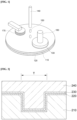
- FIG. 1 is a schematic view illustrating a manufacturing process of a semiconductor device according to an embodiment.
- a polishing pad 110 according to the embodiment is mounted on a surface plate 120
- a semiconductor substrate 130 which is a target to be polished, is disposed on the polishing pad 110.
- a polishing slurry 150 is sprayed onto the polishing pad 110 through a nozzle 140.
- a flow rate of the polishing slurry 150 supplied through the nozzle 140 may be selected according to a purpose in the range of about 10 cm 3 /min to about 1,000 cm 3 /min, and may be, for example, from about 50 cm 3 /min to about 500 cm 3 /min, but is not limited thereto.
- a polished surface of the semiconductor substrate 130 is in direct contact with a polishing surface of the polishing pad 110.
- a rotation direction of the semiconductor substrate 130 and a rotation direction of the polishing pad 110 may be the same as or be opposite to each other.
- Each of rotation speeds of the semiconductor substrate 130 and the polishing pad 110 may be selected according to a purpose in the range of about 10 rpm to about 500 rpm, and may be, for example, about 30 rpm to about 200 rpm, but is not limited thereto.
- the polishing process of the semiconductor substrate when a substrate is polished in a case of a tungsten barrier metal layer CMP process, three layers including a tungsten layer (W) as well as a silicon oxide layer (SiO 2 ) and a titanium/titanium nitride layer used as a barrier metal layer may simultaneously appear.
- the polishing composition for a semiconductor process of the present disclosure may be applied to a polishing process for a substrate from which a boron-doped polysilicon layer appears.
- polishing composition for a semiconductor process A detailed description of the polishing composition for a semiconductor process overlaps with the above description, and thus the description thereof will be omitted.
- the method for manufacturing a semiconductor device includes: providing a semiconductor substrate 130 including a boron-doped polysilicon layer and a silicon nitride layer; and polishing the boron-doped polysilicon layer and the silicon nitride layer using a polishing composition.
- the polishing composition includes water; and a polishing particle, wherein the polishing particle includes a functional group bonded to a surface of the polishing particle, the functional group includes an amine group, and a polishing selectivity of the silicon nitride layer to the boron-doped polysilicon layer is 1: 100 to 1:600.
- FIG. 2 is a cross-sectional view of a semiconductor substrate including a boron-doped polysilicon layer and a silicon nitride layer before a polishing process.
- FIG. 3 is a cross-sectional view of the semiconductor substrate including the boron-doped polysilicon layer and the silicon nitride layer polished by using a polishing composition for a semiconductor process according to an embodiment of the present disclosure.
- a trench having a vertical wall is formed, a silicon wafer 210, a silicon oxide layer 220, and a silicon nitride layer (SiN) 230 are stacked, and a boron-doped polysilicon layer (BDPSi) 240 is deposited.
- the semiconductor substrate of FIG. 2 is subjected to a polishing process using the polishing composition according to the present disclosure, and the boron-doped polysilicon layer (BDPSi) 240 is polished as shown in FIG. 3 .
- the polishing composition according to the present disclosure exhibits a high polishing rate for the boron-doped polysilicon layer (BDPSi) 240, and a low polishing rate for the silicon nitride layer (SiN) 230, as a polishing stopper layer. Due to the above properties, when the semiconductor substrate is polished by using the polishing composition according to the present disclosure, the polishing process is completed when the silicon nitride layer (SiN) 230 is exposed.
- the method for manufacturing a semiconductor device uses the polishing composition according to the present disclosure to minimize process defects by adjusting the polishing selectivity of the silicon nitride layer (SiN) to the boron-doped polysilicon layer (BDPSi) 240 as shown in FIGS. 2 and 3 , thereby providing a high-quality polished surface.
- Colloidal silica was used as the metal oxide particles.
- the colloidal silica was reacted with 3-aminopropyltriethoxysilane as a surface modifier to prepare an amino silane compound to be bonded to the surface thereof.
- a semiconductor polishing composition was prepared by using ultrapure water as a solvent, glycine as an agent for improving a polishing rate, acetic acid and/or potassium hydroxide as a pH adjusting agent, polyethylene glycol and/or a fluorine-based surfactant as a surfactant, and poly acrylic acid as a polishing inhibitor.
- composition was prepared by mixing the components in the range shown in Table 1 below based on 90 parts by weight of the solvent.
- Table 1 Metal oxide particle content Surface modifier (Amine group content (wt%) Agent for improving polishing rate (Amine group content (wt%) PH adjusting agent Surfactant Polishing inhibitor Particle size (nm) pH Viscosity (cP)
- Example 1 10 0.2 (0.0145) 0.05 (0.01067) 0.02 0.002 0.08 44 2.4 1.32
- Example 2 10 0.2 (0.0145) 0.075 (0.016) 0.02 0.002 0.08 45 2.4 1.30
- Example 3 10 0.2 (0.0145) 0.05 (0.01067) 0.02 0.001 0.08 44 2.4 1.28
- Example 4 10 0.2 (0.0145) 0.1 (0.02133) 0.02 0.002 0.08 46 2.4 1.31 Comp.
- Example 1 10 0.2 (0.0145) 0.025 (0.005333 ) 0.02 0.002 0.08 42 2.4 1.30
- Example 2 10 0.1 (0.00724) 0.05 (0.01067) 0.02 0.002 0.08 44 2.4 1.33
- Example 5 10 0.4 (0.0290) 0.05 (0.01067) 0.02 0.002 0.08 44 2.4 1.32 (unit: parts by weight)
- an HD-319B pad (SKC) with a diameter of 30 inches and a thickness of 3T was used as a polishing pad.
- the polishing was performed under the conditions of a pressure of 3.0 psi, a carrier speed of 103 rpm, a platen speed of 97 rpm, and a slurry flow rate of 300 ml/min for 60 seconds, and at the same time, conditioned at a speed of 200 rpm and for 5 minutes with a pressure of 5 lb.
- polishing rate polishing speed; A/min
- a cleaning process was performed under a chemical spraying condition of a brush rotation speed of 500 rpm and 60 s 2000 cc/min using a self-prepared cleaning chemical solution.
- the boron-doped polysilicon layer and undoped polysilicon layer, which has completely subjected the cleaning process, were sealed and total defects thereof were measured using an AIT-XP+ equipment owned by SKC.
- AFM measurement was performed using the 300 mm wafer on which defect measurement was completed.
- an average value of Ra results measured 5 times in each of 0 mm, -75 mm, +75 mm, -150 mm, and +150 mm in the position (-150 mm to +150 mm) area of the 300 mm wafer was calculated.
- Examples 1 and 2 of the present disclosure showed excellent etch rates for the boron-doped polysilicon layer, and exhibited excellent effects on defects and roughness on the wafer after the polishing process.
- an optimal polishing selectivity of the silicon nitride layer to the boron-doped polysilicon layer may be obtained by suppressing an etch rate for the silicon nitride layer.
- Example 3 had excessive defects after the polishing process, and Example 4 showed a high etch rate for the boron-doped polysilicon layer, but a high etch rate for the silicon nitride layer and a low polishing selectivity of the silicon nitride layer to the boron-doped polysilicon layer.
- Comparative Examples 1 and 2 exhibited low etch rates for boron-doped polysilicon layers, and Example 5 showed excellent etch rate for the boron-doped polysilicon layer, but had excessive defects and a high roughness value.
Landscapes
- Chemical & Material Sciences (AREA)
- Organic Chemistry (AREA)
- Engineering & Computer Science (AREA)
- Materials Engineering (AREA)
- Life Sciences & Earth Sciences (AREA)
- Wood Science & Technology (AREA)
- Composite Materials (AREA)
- Inorganic Chemistry (AREA)
- Mechanical Treatment Of Semiconductor (AREA)
- Finish Polishing, Edge Sharpening, And Grinding By Specific Grinding Devices (AREA)
Description
- The present disclosure relates to a polishing composition for a semiconductor process and a method for manufacturing a semiconductor device by using the same.
- As a semiconductor device becomes finer and denser, a technique for forming finer patterns has been used, and accordingly, surface structures of semiconductor devices have become more complicated, and steps of interlayer films have also increased. In manufacturing the semiconductor device, a chemical mechanical polishing (CMP) process is used as a planarization technology for removing a step in a specific layer formed on a substrate.
- In the CMP process, a surface of a substrate is polished while a slurry is provided to a polishing pad and the substrate is pressed and rotated. A target to be planarized varies according to a stage of a process, and there is also a difference in physical properties of the slurry applied at this time.
- Polysilicon is mainly used for a sacrificial layer in a final stage of a gate forming process in micro-electro mechanical systems (MEMS) or next-generation devices. Recently, in front end of line (FEOL) and MEMS cavity device processes of through silicon vias (TSVs), a layer having both thermal stability and mechanical stability has been required, and a layer in which polysilicon is doped with impurities at a high level has been used.
- In a case of impurity doping, boron is used as a p-type dopant, and phosphorous is used as an n-type dopant. In particular, boron is mainly used as a dopant because it is known that phosphorus suppresses a deposition rate in a chemical vapor deposition (CVD) method.
- In a case of a boron-doped polysilicon layer (BDPSi) in which boron is used as the dopant, the physical strength thereof increases as a content of boron increases, and thus there is a problem that a polishing rate is relatively very low when the CMP process is performed.
- Conventionally, in order to improve a polishing rate of a boron-doped layer, an additive containing an amine group has been used in the slurry. However, when an amine compound is added to the slurry in the form of the additive as described above, a chemical reaction occurs partially on a wafer, such that there is a problem that a defect and a variation in the polishing rate occur on the wafer.
The following prior art documents all disclose polishing compositions for semiconductor processes:US 2021/047541 A1 ,US 10 626 298 B1 US 2015/376463 A1 ,US 2009/081927 A1 ,US 2008/287038 A1 andUS 2004/209555 A1 . However, none of these documents is concerned with the specific problem of polishing boron-doped semiconductor surfaces. - There is a need to develop a polishing composition for a semiconductor process capable of improving the polishing rate of the boron-doped layer and preventing the defect and the variation in polishing rate on the wafer as described above.
- An object of the present disclosure is to provide a polishing composition for a semiconductor process and a method for polishing a substrate by using the same.
- Another object of the present disclosure is to provide a polishing composition for a semiconductor process capable of increasing a polishing rate of a boron-doped layer and improving a polishing selectivity, and a method for polishing a substrate by using the same.
- Still another object of the present disclosure is to provide a polishing composition for a semiconductor process capable of preventing a defect of a wafer that may occur in a polishing process and improving surface roughness of the wafer, and a method for polishing a substrate by using the same.
- Yet another object of the present disclosure is to provide a method for manufacturing a semiconductor device by using a polishing composition for a semiconductor process.
- In order to achieve the above object, an embodiment of the present disclosure provides a polishing composition for a semiconductor process including: water; a polishing particle, and an amine-based agent for improving a polishing rate, wherein the polishing particle includes a functional group bonded to a surface of the polishing particle, the functional group includes an amine group, and a polishing selectivity of a silicon nitride layer to a boron-doped polysilicon layer is 1: 100 to 1:600. The polishing particle is selected from the group consisting of colloidal silica, fumed silica, ceria, alumina, titania, zirconia, and mixtures thereof, included in an amount of 5 wt.% to 15 wt.%, based on the total weight of the polishing composition. Finally, the content of the amine group included in the functional group bonded to the surface of the polishing particles is 0.008 wt% to 0.06 wt%, based on the total weight of the polishing composition, and the content of the amine group included in the agent for improving a polishing rate is 0.006 wt% to 0.05 wt%, based on the total weight of the polishing composition.
- Another embodiment of the present disclosure provides a polishing composition as described above, wherein an etch rate for a boron-doped polysilicon layer is 2,000 Å/min or more.
- Still another embodiment of the present disclosure provides a method for manufacturing a semiconductor device including: providing a semiconductor substrate including a boron-doped polysilicon layer and a silicon nitride layer; and polishing the boron-doped polysilicon layer and the silicon nitride layer using a polishing composition, wherein the polishing composition is as described above.
- The present disclosure may increase a polishing rate of a boron-doped layer, improve a polishing selectivity, prevent a defect of a wafer that may occur during the polishing process, and improve surface roughness of the wafer.
- In addition, a polished semiconductor substrate may be manufactured by using a polishing composition for a semiconductor process.
-
-
FIG. 1 is a schematic view illustrating a manufacturing process of a semiconductor device according to an embodiment of the present disclosure. -
FIG. 2 is a cross-sectional view of a semiconductor substrate including a boron-doped polysilicon layer and a silicon nitride layer before a polishing process according to an embodiment of the present disclosure. -
FIG. 3 is a cross-sectional view of the semiconductor substrate including the boron-doped polysilicon layer and the silicon nitride layer polished by using a polishing composition for a semiconductor process according to an embodiment of the present disclosure. - Hereinafter, embodiments of the present disclosure will be described in detail so as to be easily carried out by those of ordinary skill in the art to which the present disclosure pertains. However, the present disclosure may be implemented in various different forms and is not limited to examples described herein.
- As used herein, when any component is referred to as "including" another component, it means the further inclusion of other components rather than the exclusion of other components, unless explicitly described to the contrary.
- As used herein, when any component is referred to as being "connected to" another component, it means that both components are "directly connected to" each other or are "connected to" each other with another component interposed therebetween.
- As used herein, "B is located on A" means that B is located directly on A or B is located on A while another layer is located therebetween and is not construed as being limited to B located in contact with the surface of A.
- As used herein, the term "combinations thereof' included in the expression of a Markush-type refers to one or more mixtures or combinations selected from the group consisting of the components described in the expression of the Markush-type, which include one or more selected from the group consisting of the above components.
- As used herein, the description of "A and/or B" means "A, B, or A and B."
- As used herein, terms such as "first" and "second" or "A" and "B" are used to distinguish the same terms from each other unless otherwise specified.
- As used herein, the singular expression is to be construed as meaning including the singular or the plural as interpreted in context unless otherwise specified.
- As used herein, "hydrogen" is hydrogen, protium, deuterium, or tritium.
- As used herein, "alkyl" refers to a monovalent substituent derived from a straight or branched chain, saturated hydrocarbon having 1 to 40 carbon atoms. Examples of the alkyl may include, but are not limited to, methyl, ethyl, propyl, isobutyl, sec-butyl, pentyl, iso-amyl, hexyl, etc.
- As used herein, "alkenyl" refers to a monovalent substituent derived from a straight or branched chain, unsaturated hydrocarbon having 2 to 40 carbon atoms and having one or more carbon-carbon double bonds. Examples of the alkenyl may include, but are not limited to, vinyl, allyl, isopropenyl, 2-butenyl, etc.
- As used herein, "alkynyl" refers to a monovalent substituent derived from a straight or branched chain, unsaturated hydrocarbon having 2 to 40 carbon atoms and having one or more carbon-carbon triple bonds. Examples of the alkynyl may include, but are not limited to, ethynyl, 2-propynyl, etc.
- As used herein, "cycloalkyl" refers to a monovalent substituent derived from a monocyclic or polycyclic non-aromatic hydrocarbon having 3 to 40 carbon atoms. Examples of the cycloalkyl may include, but are not limited to, cyclopropyl, cyclobutyl, cyclopentyl, cyclohexyl, norbornyl, adamantine, etc.
- Hereinafter, the present disclosure will be described in detail.
- A polishing composition for a semiconductor process according to an embodiment of the present disclosure includes: water; and a polishing particle, wherein the polishing particle includes a functional group bonded to a surface of the polishing particle, the functional group includes an amine group, and a polishing selectivity of a silicon nitride layer to a boron-doped polysilicon layer is 1: 100 to 1:600.
- The polishing particle according to the present disclosure may be specifically selected from the group consisting of colloidal silica, fumed silica, ceria, and a mixture thereof.
- The polishing particle may be included in an amount of 5 wt% to 15 wt%, and preferably 7 wt% to 12 wt%, based on the total weight of the polishing composition for a semiconductor process. When the polishing particle is included in the above content range, it is possible to obtain the effect of reducing instability and defects on the surface of the polished substrate at the same time.
- The polishing particle of the present disclosure includes the functional group bonded to the surface of the polishing particle, and the functional group includes a terminal amine group.
- The polishing particle includes the functional group bonded to the surface of the polishing particle, and the functional group includes the amine group, and more specifically, the terminal amine group.
- In a case of a boron-doped polysilicon layer (BDPSi) in which boron is used as a dopant, the physical strength thereof increases as a content of boron increases, and thus there is a problem that a polishing rate is relatively very low when a CMP process is performed. In order to solve such a problem, an additive containing an amine group has been conventionally used in a polishing composition. However, when an amine compound is added in the form of the additive as described above, a chemical reaction occurs partially on a wafer, such that a defect and a variation in the polishing rate may occur on the wafer.
- In the boron-doped polysilicon layer (BDPSi) in which boron is used as the dopant, boron in group 13 is added as impurities, and in this case, an amount of added boron may be 1015 to 1019 per cm3.
- Accordingly, in the present disclosure, in order to prevent the defect and the variation in the polishing rate that may occur during a polishing process of the wafer by including the amine compound as the additive, the functional group may be bonded to the surface of the metal oxide particle, and the functional group may include the terminal amine group.
- The content of the amine group is 0.0185 wt% to 0.05 wt%, based on the total weight of the polishing composition. When the amine group is bonded to the surface of the polishing particle within the above range, a polishing rate of the BDPSi may be increased, a polishing selectivity may be improved, a defect of the wafer due to the polishing process may be prevented, and surface roughness of the wafer may be improved. That is, when the amine group is included in an amount less than the above range, the effect described above may be insufficient, and when the amine group is included in an amount exceeding the above range, as in a case where the amine group is included in the form of the additive, a partial chemical reaction with the wafer may occur, such that a defect may occur and a variation in polishing rate may appear on the wafer during the polishing process.
- Specifically, in a case of the colloidal silica, silane compounds are generally used in order to modify the surface of the particle. Among these silanes, in a case of silane substituted with an amine group, a high level of negative charges may be substituted with a predetermined level of positive charges. When a modified amine group and a boron-doped polysilicon surface come into contact with a silica surface, corrosion of a doped polysilicon surface may be accelerated by catalysis. In addition, a silica particle may adjust the surface roughness of a boron-doped silicon wafer to a very low level (less than 20 Å) while physically performing a polishing action.
- It is possible to react with an amino silane compound to modify a surface of the colloidal silica to increase a polishing rate of the doped polysilicon, prevent the occurrence of the defect on the surface of the wafer, and maintain low roughness on the surface of the boron-doped silicon wafer.
- If amino silane is bonded to the particle surface of the colloidal silica, it may be bonded as functional group as follow:

- * means a portion boned to the surface of the metal oxide particles, R1 and R2 are the same as or different from each other, and are each independently selected from the group consisting of hydrogen, a substituted or unsubstituted alkyl group having 1 to 10 carbon atoms, a substituted or unsubstituted cycloalkyl group having 3 to 10 carbon atoms, a substituted or unsubstituted alkenyl group having 2 to 10 carbon atoms, and a substituted or unsubstituted alkynyl group having 2 to 10 carbon atoms, and L1 is selected from the group consisting of a substituted or unsubstituted alkylene group having 1 to 10 carbon atoms, a substituted or unsubstituted alkenylene group having 2 to 10 carbon atoms, a substituted or unsubstituted alkynylene group having 2 to 10 carbon atoms, and a substituted or unsubstituted cycloalkylene group having 3 to 10 carbon atoms.
- Specifically, R1 and R2 are the same as or different from each other, and may be each independently an alkyl group having 1 to 10 carbon atoms, and L1 may be a substituted or unsubstituted alkylene group having 1 to 10 carbon atoms.
- The amino silane may be, for example, any one selected from the group consisting of 3-aminopropyltriethoxysilane, bis[(3-triethoxysilyl)propyl]amine, 3-aminopropyltrimethoxysilane, bis[(3-trimethoxysilyl)propyl]amine, 3-aminopropylmethyldiethoxysilane, 3-aminopropylmethyldimethoxysilane, N-[3-(trimethoxysilyl)propyl]ethylenediamine, N-bis[3-(trimethoxysilyl)propyl]-1,2-ethylenediamine, N-[3-(triethoxysilyl)propyl]ethylenediamine, diethylenetriaminopropyltrimethoxysilane, diethylenetriaminopropylmethyldimethoxysilane, diethylaminomethyltriethoxysilane, diethylaminopropyltrimethoxysilane, diethylaminopropyltriethoxysilane, dimethylaminopropyltrimethoxysilane, N-[3-(trimethoxysilyl)propyl]butylamine, and combinations thereof.
- Specifically, the amino silane used for surface modification of colloidal silica may be aminopropyltriethoxysilane, but the present disclosure is not limited to the above examples, and amino silane capable of preventing the polishing rate and surface defects of boron-doped silicon wafers may be used without limitation.
- The amino silane compound may be included in an amount of 0.15 wt% to 0.3 wt%, preferably 0.15 wt% to 0.25 wt%, based on the total weight of the polishing composition for a semiconductor process. When the amino silane compound is included within the above range, a sufficient polishing rate for BDPSi may be exhibited by bonding an amine group to the surface of the polishing particle. When the amino silane compound is included in an amount exceeding the above range, the polishing rate for BDPSi may be increased, but the polishing particle and unreacted amino silane compound may remain due to excessive addition, and the remaining amino silane compound may be adsorbed on the surface of the wafer, resulting in a defect.
- In addition, in order for a physically surface-modified colloidal silica particle to adjust the roughness of the surface of BDPSi to a very low level of less than 20 Å while physically performing a polishing action, during a catalytic action between the surface of the polishing particle and a target film, the extent or size of the catalytic reaction needs to be increased depending on the roughness of the target film.
- In this case, the catalytic reaction on the modified surface of the particles may not be sufficient to control the roughness of the entire area of the wafer. That is, it cannot exhibit a very low level of surface roughness as in the present disclosure. In order to solve this, an additional additive is required in addition to the modified surface of the particles when the slurry is prepared.
- In another embodiment of the present disclosure, a polishing composition for a semiconductor process includes: water; a polishing particle surface-treated with a functional group including an amine group; and an amine-based agent for improving a polishing rate, wherein the etch rate to the boron-doped polysilicon layer is 2,000 Å/min or more.
- The additive included in order to exhibit a very low level of surface roughness as described above is specifically an amine-based agent for improving a polishing rate.
- Specifically, based on the total weight of the composition, the content of the amine group included in the functional group bonded to the surface of the polishing particles is 0.008 wt% to 0.06 wt%, and the content of the amine group included in the agent for improving a polishing rate is 0.006 wt% to 0.05 wt%. The amine group, which is a functional group bonded to the surface of the polishing particles, has a slightly lower content range as the agent for improving a polishing rate is additionally included based on the total weight of the composition. When the amine group is included within the above range, a polishing rate of the BDPSi may be increased, a polishing selectivity may be improved, a defect of the wafer due to the polishing process may be prevented, and surface roughness of the wafer may be improved.
- The agent for improving a polishing rate may be more specifically selected from the group consisting of glycine, β-alanine betaine, stearyl betaine, and a mixture thereof, and preferably glycine, but the present disclosure is not limited to the examples.
- The agent for improving a polishing rate may be included in the polishing composition together with the surface-modified polishing particle to increase the polishing rate for BDPSi, and exhibit a very low level of surface roughness.
- The agent for improving a polishing rate may be included in an amount of 0.03 wt% to 0.095 wt%, preferably 0.05 wt% to 0.08 wt%, based on the total weight of the polishing composition for a semiconductor process. When the agent for improving a polishing rate is mixed within the above range, it is possible to not only exhibit a high etch rate for BDPSi but also to control the polishing selectivity with the silicon nitride layer.
- The polishing composition may have an etch rate for BDPSi of 2,000 Å/min or more, and an etch rate for the silicon nitride layer of 100 Å/min or less.
- Specifically, the polishing composition of the present disclosure may have an etch rate for BDPSi of 2,000 Å/min or more, and preferably 2,100 Å/min or more, thereby exhibiting an excellent etch rate, and a low etch rate for a silicon nitride layer.
- The polishing composition for a semiconductor process according to the present disclosure is characterized in that the polishing selectivity of the silicon nitride layer (SiN) to the polysilicon layer is 1:50 to 1:600, preferably 1:50 to 1:200, and more preferably 1:50 to 1:100. Specifically, the polysilicon layer is BDPSi, and BDPSi as described above has a problem in that the physical strength thereof is increased due to boron doping, so that the polishing rate is relatively low during the polishing process.
- By improving such a problem, it is necessary to increase the polishing rate for BDPSi, and exhibit a low polishing rate for the silicon nitride layer as a polishing stopper layer. In order to exhibit the polishing selectivity of the polishing composition of the present disclosure, a semiconductor substrate is a wafer with a diameter of 300 mm having a thickness of the silicon nitride (SiN) of 1,500 Å by depositing SiN on a bare silicon wafer.
- Specifically, the BDPSi is polished by using the silicon nitride layer as the polishing stopper layer. If the polishing selectivity is not adjusted as described above, process defects such as dishing and erosion may occur. Therefore, as in the present disclosure, a high-quality polished surface may be provided by adjusting the polishing selectivity of the silicon nitride layer (SiN) to the BDPSi to minimize process defects.
- In order to suppress the polishing of the silicon nitride layer, the polishing composition according to the present disclosure includes a polishing inhibitor, wherein the polishing inhibitor may be selected from the group consisting of polyacrylic acid, polyphosphoric acid, polymaleic acid, polymethacrylic acid, polyacrylamide-co-acrylic acid, polyacrylic acid-co-maleic acid, polyacrylamide-co-acrylic acid, and a mixture thereof, and is preferably polyacrylic acid, but the present disclosure is not limited to the examples, and any composition that can be used as a polishing inhibitor by a person skilled in the art may be used without limitation.
- The polishing inhibitor is included in an amount of 0.05 wt% to 0.1 wt%, preferably 0.06 wt% to 0.09 wt%, based on the total weight of the polishing composition for a semiconductor process. When the polishing inhibitor is mixed within the above range, the polishing selectivity of the silicon nitride layer for the BDPSi may be adjusted by suppressing polishing of the silicon nitride layer.
- The polishing composition may further include a surfactant. The surfactant may be a nonionic surfactant.
- The non-ionic surfactant may be selected from the group consisting of polyethylene glycol, polypropylene glycol, polyethylene-propylene copolymer, polyalkyl oxide, polyoxyethylene oxide (PEO), polyethylene oxide, and polypropylene oxide; and a fluorine-based surfactant may be selected from the group consisting of a sodium sulfonate fluorosurfactant, a phosphate ester fluorosurfactant, an amine oxide fluorosurfactant, a betaine fluorosurfactant, an ammonium carboxylate fluorosurfactant, a stearate ester fluorosurfactant, a quaternary ammonium fluorosurfactant, an ethylene oxide/propylene oxide fluorosurfactant, and a polyoxyethylene fluorosurfactant.
- The surfactant may be included in an amount of 0.0015 wt% to 0.005 wt%, preferably 0.0015 wt% to 0.003 wt%, based on the total weight of the polishing composition for a semiconductor process. When the surfactant is mixed within the above range, the occurrence of defects on the wafer surface by the polishing process may be suppressed.
- The polishing composition of the present disclosure may include a pH adjusting agent, and the pH adjusting agent may be any one selected from the group consisting of hydrochloric acid, phosphoric acid, sulfuric acid, hydrofluoric acid, hydrobromic acid, iodic acid, formic acid, malonic acid, maleic acid, oxalic acid, acetic acid, adipic acid, citric acid, adipic acid, acetic acid, propionic acid, fumaric acid, lactic acid, salicylic acid, pimeline, benzoic acid, succinic acid, phthalic acid, butyric acid, glutaric acid, glutamic acid, glycolic acid, lactic acid, aspartic acid, tartaric acid, and potassium hydroxide.
- The pH adjusting agent may be included in an amount of 0.01 wt% to 0.05 wt%, based on the total weight of the polishing composition for a semiconductor process. The polishing composition for a semiconductor process may have a pH of 2 to 5, and preferably 2 to 3. When the acidic environment is maintained within the above range, excessive corrosion of metal components or polishing equipments may be prevented while maintaining the polishing rate and quality to a certain level or higher.
- The polishing composition for a semiconductor process includes a solvent as a remaining component except for the components described above and additional components to be described later. The solvent may be water, preferably ultrapure water is applied. The solvent may be included in the content range of the remainder of the content ranges of a polishing particle, a surface modifier, an agent for improving a polishing rate, a pH adjusting agent, a surfactant, and a polishing inhibitor.
-
FIG. 1 is a schematic view illustrating a manufacturing process of a semiconductor device according to an embodiment. Referring toFIG. 1 , after apolishing pad 110 according to the embodiment is mounted on asurface plate 120, asemiconductor substrate 130, which is a target to be polished, is disposed on thepolishing pad 110. For polishing, a polishingslurry 150 is sprayed onto thepolishing pad 110 through anozzle 140. - A flow rate of the polishing
slurry 150 supplied through thenozzle 140 may be selected according to a purpose in the range of about 10 cm3/min to about 1,000 cm3/min, and may be, for example, from about 50 cm3/min to about 500 cm3/min, but is not limited thereto. - A polished surface of the
semiconductor substrate 130 is in direct contact with a polishing surface of thepolishing pad 110. - Thereafter, the
semiconductor substrate 130 and thepolishing pad 110 are rotated relative to each other, such that the surface of thesemiconductor substrate 130 may be polished. In this case, a rotation direction of thesemiconductor substrate 130 and a rotation direction of thepolishing pad 110 may be the same as or be opposite to each other. Each of rotation speeds of thesemiconductor substrate 130 and thepolishing pad 110 may be selected according to a purpose in the range of about 10 rpm to about 500 rpm, and may be, for example, about 30 rpm to about 200 rpm, but is not limited thereto. - As an example of the polishing process of the semiconductor substrate, when a substrate is polished in a case of a tungsten barrier metal layer CMP process, three layers including a tungsten layer (W) as well as a silicon oxide layer (SiO2) and a titanium/titanium nitride layer used as a barrier metal layer may simultaneously appear. The polishing composition for a semiconductor process of the present disclosure may be applied to a polishing process for a substrate from which a boron-doped polysilicon layer appears.
- A detailed description of the polishing composition for a semiconductor process overlaps with the above description, and thus the description thereof will be omitted.
- In an embodiment, the method for manufacturing a semiconductor device includes: providing a
semiconductor substrate 130 including a boron-doped polysilicon layer and a silicon nitride layer; and polishing the boron-doped polysilicon layer and the silicon nitride layer using a polishing composition. Here, the polishing composition includes water; and a polishing particle, wherein the polishing particle includes a functional group bonded to a surface of the polishing particle, the functional group includes an amine group, and a polishing selectivity of the silicon nitride layer to the boron-doped polysilicon layer is 1: 100 to 1:600. - The method for manufacturing a semiconductor device may be confirmed in more detail with reference to
FIGS. 2 and3 .FIG. 2 is a cross-sectional view of a semiconductor substrate including a boron-doped polysilicon layer and a silicon nitride layer before a polishing process.FIG. 3 is a cross-sectional view of the semiconductor substrate including the boron-doped polysilicon layer and the silicon nitride layer polished by using a polishing composition for a semiconductor process according to an embodiment of the present disclosure. - Referring to
FIG. 2 , in the semiconductor substrate, a trench having a vertical wall is formed, asilicon wafer 210, asilicon oxide layer 220, and a silicon nitride layer (SiN) 230 are stacked, and a boron-doped polysilicon layer (BDPSi) 240 is deposited. The semiconductor substrate ofFIG. 2 is subjected to a polishing process using the polishing composition according to the present disclosure, and the boron-doped polysilicon layer (BDPSi) 240 is polished as shown inFIG. 3 . The polishing composition according to the present disclosure exhibits a high polishing rate for the boron-doped polysilicon layer (BDPSi) 240, and a low polishing rate for the silicon nitride layer (SiN) 230, as a polishing stopper layer. Due to the above properties, when the semiconductor substrate is polished by using the polishing composition according to the present disclosure, the polishing process is completed when the silicon nitride layer (SiN) 230 is exposed. The method for manufacturing a semiconductor device uses the polishing composition according to the present disclosure to minimize process defects by adjusting the polishing selectivity of the silicon nitride layer (SiN) to the boron-doped polysilicon layer (BDPSi) 240 as shown inFIGS. 2 and3 , thereby providing a high-quality polished surface. - Colloidal silica was used as the metal oxide particles. The colloidal silica was reacted with 3-aminopropyltriethoxysilane as a surface modifier to prepare an amino silane compound to be bonded to the surface thereof.
- A semiconductor polishing composition was prepared by using ultrapure water as a solvent, glycine as an agent for improving a polishing rate, acetic acid and/or potassium hydroxide as a pH adjusting agent, polyethylene glycol and/or a fluorine-based surfactant as a surfactant, and poly acrylic acid as a polishing inhibitor.
- The composition was prepared by mixing the components in the range shown in Table 1 below based on 90 parts by weight of the solvent.
[Table 1] Metal oxide particle content Surface modifier (Amine group content (wt%) Agent for improving polishing rate (Amine group content (wt%) PH adjusting agent Surfactant Polishing inhibitor Particle size (nm) pH Viscosity (cP) Example 1 10 0.2 (0.0145) 0.05 (0.01067) 0.02 0.002 0.08 44 2.4 1.32 Example 2 10 0.2 (0.0145) 0.075 (0.016) 0.02 0.002 0.08 45 2.4 1.30 Example 3 10 0.2 (0.0145) 0.05 (0.01067) 0.02 0.001 0.08 44 2.4 1.28 Example 4 10 0.2 (0.0145) 0.1 (0.02133) 0.02 0.002 0.08 46 2.4 1.31 Comp. Example 1 10 0.2 (0.0145) 0.025 (0.005333 ) 0.02 0.002 0.08 42 2.4 1.30 Comp. Example 2 10 0.1 (0.00724) 0.05 (0.01067) 0.02 0.002 0.08 44 2.4 1.33 Example 5 10 0.4 (0.0290) 0.05 (0.01067) 0.02 0.002 0.08 44 2.4 1.32 (unit: parts by weight) - A polishing evaluation was performed on a boron-doped polysilicon layer (average roughness Ra = 16 Å immediately after deposition), wherein the wafer had a diameter of 300 mm and a thickness of about 6,000 Å. Specifically, an HD-319B pad (SKC) with a diameter of 30 inches and a thickness of 3T was used as a polishing pad. The polishing was performed under the conditions of a pressure of 3.0 psi, a carrier speed of 103 rpm, a platen speed of 97 rpm, and a slurry flow rate of 300 ml/min for 60 seconds, and at the same time, conditioned at a speed of 200 rpm and for 5 minutes with a pressure of 5 lb.
- An additional polishing evaluation was performed on a silicon nitride layer having a thickness of about 1,500 Å under the same polishing conditions.
- After the polishing process was performed, the thickness of each wafer was measured, and the polishing rate (polishing speed; A/min) of the slurry composition was calculated therefrom.
- After polishing was performed under the same conditions as in the CMP evaluation, a cleaning process was performed under a chemical spraying condition of a brush rotation speed of 500 rpm and 60 s 2000 cc/min using a self-prepared cleaning chemical solution. The boron-doped polysilicon layer and undoped polysilicon layer, which has completely subjected the cleaning process, were sealed and total defects thereof were measured using an AIT-XP+ equipment owned by SKC.
- AFM measurement was performed using the 300 mm wafer on which defect measurement was completed. For AFM measurement conditions, an average value of Ra results measured 5 times in each of 0 mm, -75 mm, +75 mm, -150 mm, and +150 mm in the position (-150 mm to +150 mm) area of the 300 mm wafer was calculated.
- The polishing evaluation results are shown in Table 2 below.
[Table 2] Etch rate for boron-doped polysilicon layer Defect of boron-doped polysilicon layer Roughness of boron-doped polysilicon layer Etch rate for silicon nitride layer Polishing selectivity (BDPSi/SiN) (BDPSi, A/min) (ea) (Ra, Å) (SiN, A/min) Example 1 2629 62 0.6 23 114 Example 2 2944 77 0.7 28 105 Example 3 2543 423 12.3 24 105 Example 4 3221 61 14.2 65 49 Comp. Example 1 984 66 0.7 47 21 Comp. Example 2 355 64 0.5 35 10 Example 5 2140 224 5.1 113 19 - According to Table 2, Examples 1 and 2 of the present disclosure showed excellent etch rates for the boron-doped polysilicon layer, and exhibited excellent effects on defects and roughness on the wafer after the polishing process. In addition, an optimal polishing selectivity of the silicon nitride layer to the boron-doped polysilicon layer may be obtained by suppressing an etch rate for the silicon nitride layer.
- On the other hand, Example 3 had excessive defects after the polishing process, and Example 4 showed a high etch rate for the boron-doped polysilicon layer, but a high etch rate for the silicon nitride layer and a low polishing selectivity of the silicon nitride layer to the boron-doped polysilicon layer.
- It was confirmed that Comparative Examples 1 and 2 exhibited low etch rates for boron-doped polysilicon layers, and Example 5 showed excellent etch rate for the boron-doped polysilicon layer, but had excessive defects and a high roughness value.
- Although preferred embodiments of the present disclosure have been described in detail hereinabove, the scope of the present disclosure is not limited thereto, but may also include several modifications and alterations made by those skilled in the art using a basic concept of the present disclosure as defined in the claims.
Claims (13)
- A polishing composition for a semiconductor process, comprising:water; and
a polishing particle selected from the group consisting of colloidal silica, fumed silica, ceria, alumina, titania, zirconia, and mixtures thereof, included in an amount of 5 wt.% to 15 wt.%, based on the total weight of the polishing composition, andan amine-based agent for improving a polishing rate,wherein the polishing particle includes a functional group bonded to a surface of the polishing particle,the functional group includes an amine group, andwherein the content of the amine group included in the functional group bonded to the surface of the polishing particles is 0.008 wt% to 0.06 wt%, based on the total weight of the polishing composition, andthe content of the amine group included in the agent for improving a polishing rate is 0.006 wt% to 0.05 wt%, based on the total weight of the polishing composition, andwherein a polishing selectivity of a silicon nitride layer to a boron-doped polysilicon layer is 1: 100 to 1:600. - The polishing composition of claim 1, wherein the content of the amine group is 0.0185 wt% to 0.05 wt%, based on the total weight of the polishing composition.
- The polishing composition of claim 1 or 2, wherein the functional group bonded to the surface of the polishing particle includes the following structure of Formula 1:

 * means a portion boned to the surface of metal oxide particles,R1 and R2 are the same as or different from each other, and are each independently selected from the group consisting of hydrogen, a substituted or unsubstituted alkyl group having 1 to 10 carbon atoms, a substituted or unsubstituted cycloalkyl group having 3 to 10 carbon atoms, a substituted or unsubstituted alkenyl group having 2 to 10 carbon atoms, and a substituted or unsubstituted alkynyl group having 2 to 10 carbon atoms, andL1 is selected from the group consisting of a substituted or unsubstituted alkylene group having 1 to 10 carbon atoms, a substituted or unsubstituted alkenylene group having 2 to 10 carbon atoms, a substituted or unsubstituted alkynylene group having 2 to 10 carbon atoms, and a substituted or unsubstituted cycloalkylene group having 3 to 10 carbon atoms.
 - The polishing composition of claim 3, wherein R1 and R2 are the same as or different from each other, and are each independently an alkyl group having 1 to 10 carbon atoms.
- The polishing composition of claim 3 or 4, wherein L1 is a substituted or unsubstituted alkylene group having 1 to 10 carbon atoms.
- The polishing composition of claim 1, further comprising a polishing inhibitor for the silicon nitride layer.
- The polishing composition of any one of claims 1 to 6, further comprising a surfactant.
- The polishing composition of claim 7, wherein the surfactant is included in an amount of 0.0015 wt% to 0.005 wt%, based on the total weight of the polishing composition.
- The polishing composition of any one of claims 1 to 8, further comprising a pH adjusting agent.
- The polishing composition of any one of claims 1 to 9, having a pH of 2 to 5.
- The polishing composition of any one of claims 1 to 10, having an etch rate for the silicon nitride layer of 100 Å/min or less.
- A polishing composition for a semiconductor process according to any one of claims 1 to 11, whereinthe polishing particle is surface-treated with a functional group including an amine group; and
wherein an etch rate for a boron-doped polysilicon layer is 2,000 Å/min or more. - A method for manufacturing a semiconductor device, comprising:providing a semiconductor substrate including a boron-doped polysilicon layer and a silicon nitride layer; andpolishing the boron-doped polysilicon layer and the silicon nitride layer using a polishing composition,wherein the polishing composition is as defined in any claim 1 to 12.
Applications Claiming Priority (1)
| Application Number | Priority Date | Filing Date | Title |
|---|---|---|---|
| KR1020210056409A KR20220149148A (en) | 2021-04-30 | 2021-04-30 | Polishing compostion for semiconductor process and method for manufacturing semiconductor device by using the same |
Publications (2)
| Publication Number | Publication Date |
|---|---|
| EP4086312A1 EP4086312A1 (en) | 2022-11-09 |
| EP4086312B1 true EP4086312B1 (en) | 2024-06-19 |
Family
ID=81392968
Family Applications (1)
| Application Number | Title | Priority Date | Filing Date |
|---|---|---|---|
| EP22170427.3A Active EP4086312B1 (en) | 2021-04-30 | 2022-04-28 | Polishing composition for semiconductor process and method for manufacturing semiconductor device by using the same |
Country Status (6)
| Country | Link |
|---|---|
| US (1) | US12116503B2 (en) |
| EP (1) | EP4086312B1 (en) |
| JP (1) | JP7494243B2 (en) |
| KR (2) | KR20220149148A (en) |
| CN (1) | CN115260911B (en) |
| TW (1) | TWI849416B (en) |
Families Citing this family (5)
| Publication number | Priority date | Publication date | Assignee | Title |
|---|---|---|---|---|
| KR102638622B1 (en) * | 2021-07-22 | 2024-02-19 | 에스케이엔펄스 주식회사 | Polishing compostion for semiconductor process and method for manufacturing semiconductor device by using the same |
| KR20230055586A (en) * | 2021-10-19 | 2023-04-26 | 에스케이하이닉스 주식회사 | Chemical mechanical polishing slurry composition for polishing boron silicon compound, chemical mechanical polishing method and method of fabricating semiconductor device using the same |
| JP2024126825A (en) * | 2023-03-08 | 2024-09-20 | 株式会社フジミインコーポレーテッド | Polishing composition, polishing method, method for producing semiconductor substrate, and agent for suppressing polishing rate of object having silicon-nitrogen bond |
| CN122003477A (en) * | 2023-09-05 | 2026-05-08 | 恩特格里斯公司 | Titanium oxide-based chemical mechanical polishing composition for highly boron-doped silicon films |
| KR20250048914A (en) * | 2023-10-04 | 2025-04-11 | 에스케이엔펄스 주식회사 | Polishing composition for semiconductor process and polishing method of substrate using the same |
Family Cites Families (18)
| Publication number | Priority date | Publication date | Assignee | Title |
|---|---|---|---|---|
| JP4954398B2 (en) * | 2001-08-09 | 2012-06-13 | 株式会社フジミインコーポレーテッド | Polishing composition and polishing method using the same |
| US7044836B2 (en) * | 2003-04-21 | 2006-05-16 | Cabot Microelectronics Corporation | Coated metal oxide particles for CMP |
| KR100642391B1 (en) | 2005-04-04 | 2006-11-03 | 주식회사 하이닉스반도체 | Chemical Mechanical Polishing Method for Manufacturing Semiconductor Devices |
| JP2008288398A (en) * | 2007-05-18 | 2008-11-27 | Nippon Chem Ind Co Ltd | Semiconductor wafer polishing composition, method for producing the same, and polishing method |
| SG184772A1 (en) * | 2007-09-21 | 2012-10-30 | Cabot Microelectronics Corp | Polishing composition and method utilizing abrasive particles treated with an aminosilane |
| JP2011216582A (en) * | 2010-03-31 | 2011-10-27 | Fujifilm Corp | Polishing method and polishing liquid |
| TWI573864B (en) * | 2012-03-14 | 2017-03-11 | 卡博特微電子公司 | CMP composition selective for oxides and nitrides with high removal rate and low defect rate |
| KR20150009914A (en) * | 2013-07-17 | 2015-01-27 | 삼성전자주식회사 | CMP composition for polishing an organic layer and method of forming a semiconductor device using the composition |
| KR20160057397A (en) * | 2013-09-20 | 2016-05-23 | 가부시키가이샤 후지미인코퍼레이티드 | Polishing composition |
| TWI564380B (en) * | 2014-06-25 | 2017-01-01 | 卡博特微電子公司 | Copper barrier layer chemical mechanical polishing composition |
| CN106928859A (en) * | 2015-12-31 | 2017-07-07 | 安集微电子科技(上海)有限公司 | A kind of chemical mechanical polishing liquid and its application |
| TWI829666B (en) * | 2018-03-15 | 2024-01-21 | 日商福吉米股份有限公司 | Polishing composition, polishing composition manufacturing method, polishing method and semiconductor substrate manufacturing method |
| JP7250530B2 (en) * | 2018-03-15 | 2023-04-03 | 株式会社フジミインコーポレーテッド | Polishing composition, method for producing polishing composition, polishing method, and method for producing semiconductor substrate |
| JP7120780B2 (en) * | 2018-03-20 | 2022-08-17 | 株式会社フジミインコーポレーテッド | Polishing composition and polishing method using the same |
| US10763119B2 (en) * | 2018-12-19 | 2020-09-01 | Fujifilm Electronic Materials U.S.A., Inc. | Polishing compositions and methods of using same |
| US10626298B1 (en) * | 2019-03-20 | 2020-04-21 | Rohm And Haas Electronic Materials Cmp Holdings, Inc. | Chemical mechanical polishing compositions and methods for suppressing the removal rate of amorphous silicon |
| US20200303198A1 (en) * | 2019-03-22 | 2020-09-24 | Fujimi Incorporated | Polishing composition and polishing method |
| JP7267893B2 (en) * | 2019-03-27 | 2023-05-02 | 株式会社フジミインコーポレーテッド | Polishing composition |
-
2021
- 2021-04-30 KR KR1020210056409A patent/KR20220149148A/en not_active Ceased
-
2022
- 2022-04-27 CN CN202210454337.4A patent/CN115260911B/en active Active
- 2022-04-27 JP JP2022073393A patent/JP7494243B2/en active Active
- 2022-04-28 EP EP22170427.3A patent/EP4086312B1/en active Active
- 2022-04-29 TW TW111116338A patent/TWI849416B/en active
- 2022-05-01 US US17/734,073 patent/US12116503B2/en active Active
-
2024
- 2024-05-02 KR KR1020240058426A patent/KR102853753B1/en active Active
Also Published As
| Publication number | Publication date |
|---|---|
| US20220363948A1 (en) | 2022-11-17 |
| EP4086312A1 (en) | 2022-11-09 |
| KR20220149148A (en) | 2022-11-08 |
| JP2022171615A (en) | 2022-11-11 |
| JP7494243B2 (en) | 2024-06-03 |
| KR20240063849A (en) | 2024-05-10 |
| CN115260911A (en) | 2022-11-01 |
| US12116503B2 (en) | 2024-10-15 |
| KR102853753B1 (en) | 2025-09-01 |
| TWI849416B (en) | 2024-07-21 |
| CN115260911B (en) | 2024-06-07 |
| TW202244242A (en) | 2022-11-16 |
Similar Documents
| Publication | Publication Date | Title |
|---|---|---|
| EP4086312A1 (en) | Polishing composition for semiconductor process and method for manufacturing semiconductor device by using the same | |
| KR101718814B1 (en) | A Slurry Composition Having Tunable Dielectric Polishing Selectivity and Method of Polishing a Substrate | |
| KR101718788B1 (en) | Chemical Mechanical Polishing Composition and Methods Relating Thereto | |
| JP5957777B2 (en) | Method for polishing a substrate comprising polysilicon, silicon oxide and silicon nitride | |
| EP4122991A2 (en) | Polishing pad and method for manufacturing semiconductor device using same | |
| US7700489B2 (en) | Method of manufacturing a semiconductor device | |
| CN111718657B (en) | Chemical mechanical polishing composition and method of inhibiting the removal rate of amorphous silicon | |
| EP4067449A1 (en) | Polishing composition for semiconductor process and method for manufacturing semiconductor device by using the same | |
| KR102774598B1 (en) | Polishing compostion for semiconductor process and method for manufacturing semiconductor device by using the same | |
| KR20230112263A (en) | Composition for semiconduct process, method for preparing thereof and manufacturing method of semiconduct device using the same | |
| JP2020120117A (en) | Acid polishing composition with enhanced defect suppression and method for polishing substrate | |
| US20220098441A1 (en) | Polishing composition, method for producing the same, polishing method, and method for producing substrate | |
| US20230374346A1 (en) | Surface-modified silica particles and compositions comprising such particles | |
| JP2006165142A (en) | Chemical mechanical polishing aqueous dispersion and chemical mechanical polishing method | |
| KR20190063661A (en) | Chemical-mechanical polishing slurry composition and method for manufacturing semiconductor by using the same | |
| KR20170072532A (en) | Chemical mechanical polishing slurry and polishing method using the same |
Legal Events
| Date | Code | Title | Description |
|---|---|---|---|
| PUAI | Public reference made under article 153(3) epc to a published international application that has entered the european phase |
Free format text: ORIGINAL CODE: 0009012 |
|
| STAA | Information on the status of an ep patent application or granted ep patent |
Free format text: STATUS: REQUEST FOR EXAMINATION WAS MADE |
|
| 17P | Request for examination filed |
Effective date: 20220428 |
|
| AK | Designated contracting states |
Kind code of ref document: A1 Designated state(s): AL AT BE BG CH CY CZ DE DK EE ES FI FR GB GR HR HU IE IS IT LI LT LU LV MC MK MT NL NO PL PT RO RS SE SI SK SM TR |
|
| STAA | Information on the status of an ep patent application or granted ep patent |
Free format text: STATUS: EXAMINATION IS IN PROGRESS |
|
| RAP3 | Party data changed (applicant data changed or rights of an application transferred) |
Owner name: SK ENPULSE CO., LTD. |
|
| RBV | Designated contracting states (corrected) |
Designated state(s): AL AT BE BG CH CY CZ DE DK EE ES FI FR GB GR HR HU IE IS IT LI LT LU LV MC MK MT NL NO PL PT RO RS SE SI SK SM TR |
|
| 17Q | First examination report despatched |
Effective date: 20230531 |
|
| P01 | Opt-out of the competence of the unified patent court (upc) registered |
Effective date: 20230622 |
|
| GRAP | Despatch of communication of intention to grant a patent |
Free format text: ORIGINAL CODE: EPIDOSNIGR1 |
|
| STAA | Information on the status of an ep patent application or granted ep patent |
Free format text: STATUS: GRANT OF PATENT IS INTENDED |
|
| INTG | Intention to grant announced |
Effective date: 20240130 |
|
| GRAS | Grant fee paid |
Free format text: ORIGINAL CODE: EPIDOSNIGR3 |
|
| GRAA | (expected) grant |
Free format text: ORIGINAL CODE: 0009210 |
|
| STAA | Information on the status of an ep patent application or granted ep patent |
Free format text: STATUS: THE PATENT HAS BEEN GRANTED |
|
| AK | Designated contracting states |
Kind code of ref document: B1 Designated state(s): AL AT BE BG CH CY CZ DE DK EE ES FI FR GB GR HR HU IE IS IT LI LT LU LV MC MK MT NL NO PL PT RO RS SE SI SK SM TR |
|
| REG | Reference to a national code |
Ref country code: GB Ref legal event code: FG4D |
|
| REG | Reference to a national code |
Ref country code: CH Ref legal event code: EP |
|
| REG | Reference to a national code |
Ref country code: DE Ref legal event code: R096 Ref document number: 602022003988 Country of ref document: DE |
|
| REG | Reference to a national code |
Ref country code: SE Ref legal event code: TRGR |
|
| PG25 | Lapsed in a contracting state [announced via postgrant information from national office to epo] |
Ref country code: BG Free format text: LAPSE BECAUSE OF FAILURE TO SUBMIT A TRANSLATION OF THE DESCRIPTION OR TO PAY THE FEE WITHIN THE PRESCRIBED TIME-LIMIT Effective date: 20240619 |
|
| PG25 | Lapsed in a contracting state [announced via postgrant information from national office to epo] |
Ref country code: FI Free format text: LAPSE BECAUSE OF FAILURE TO SUBMIT A TRANSLATION OF THE DESCRIPTION OR TO PAY THE FEE WITHIN THE PRESCRIBED TIME-LIMIT Effective date: 20240619 Ref country code: HR Free format text: LAPSE BECAUSE OF FAILURE TO SUBMIT A TRANSLATION OF THE DESCRIPTION OR TO PAY THE FEE WITHIN THE PRESCRIBED TIME-LIMIT Effective date: 20240619 |
|
| REG | Reference to a national code |
Ref country code: LT Ref legal event code: MG9D |
|
| PG25 | Lapsed in a contracting state [announced via postgrant information from national office to epo] |
Ref country code: GR Free format text: LAPSE BECAUSE OF FAILURE TO SUBMIT A TRANSLATION OF THE DESCRIPTION OR TO PAY THE FEE WITHIN THE PRESCRIBED TIME-LIMIT Effective date: 20240920 |
|
| REG | Reference to a national code |
Ref country code: NL Ref legal event code: MP Effective date: 20240619 |
|
| PG25 | Lapsed in a contracting state [announced via postgrant information from national office to epo] |
Ref country code: LV Free format text: LAPSE BECAUSE OF FAILURE TO SUBMIT A TRANSLATION OF THE DESCRIPTION OR TO PAY THE FEE WITHIN THE PRESCRIBED TIME-LIMIT Effective date: 20240619 |
|
| PG25 | Lapsed in a contracting state [announced via postgrant information from national office to epo] |
Ref country code: NO Free format text: LAPSE BECAUSE OF FAILURE TO SUBMIT A TRANSLATION OF THE DESCRIPTION OR TO PAY THE FEE WITHIN THE PRESCRIBED TIME-LIMIT Effective date: 20240919 Ref country code: LV Free format text: LAPSE BECAUSE OF FAILURE TO SUBMIT A TRANSLATION OF THE DESCRIPTION OR TO PAY THE FEE WITHIN THE PRESCRIBED TIME-LIMIT Effective date: 20240619 Ref country code: HR Free format text: LAPSE BECAUSE OF FAILURE TO SUBMIT A TRANSLATION OF THE DESCRIPTION OR TO PAY THE FEE WITHIN THE PRESCRIBED TIME-LIMIT Effective date: 20240619 Ref country code: GR Free format text: LAPSE BECAUSE OF FAILURE TO SUBMIT A TRANSLATION OF THE DESCRIPTION OR TO PAY THE FEE WITHIN THE PRESCRIBED TIME-LIMIT Effective date: 20240920 Ref country code: FI Free format text: LAPSE BECAUSE OF FAILURE TO SUBMIT A TRANSLATION OF THE DESCRIPTION OR TO PAY THE FEE WITHIN THE PRESCRIBED TIME-LIMIT Effective date: 20240619 Ref country code: BG Free format text: LAPSE BECAUSE OF FAILURE TO SUBMIT A TRANSLATION OF THE DESCRIPTION OR TO PAY THE FEE WITHIN THE PRESCRIBED TIME-LIMIT Effective date: 20240619 Ref country code: RS Free format text: LAPSE BECAUSE OF FAILURE TO SUBMIT A TRANSLATION OF THE DESCRIPTION OR TO PAY THE FEE WITHIN THE PRESCRIBED TIME-LIMIT Effective date: 20240919 |
|
| PG25 | Lapsed in a contracting state [announced via postgrant information from national office to epo] |
Ref country code: NL Free format text: LAPSE BECAUSE OF FAILURE TO SUBMIT A TRANSLATION OF THE DESCRIPTION OR TO PAY THE FEE WITHIN THE PRESCRIBED TIME-LIMIT Effective date: 20240619 |
|
| REG | Reference to a national code |
Ref country code: AT Ref legal event code: MK05 Ref document number: 1695906 Country of ref document: AT Kind code of ref document: T Effective date: 20240619 |
|
| PG25 | Lapsed in a contracting state [announced via postgrant information from national office to epo] |
Ref country code: NL Free format text: LAPSE BECAUSE OF FAILURE TO SUBMIT A TRANSLATION OF THE DESCRIPTION OR TO PAY THE FEE WITHIN THE PRESCRIBED TIME-LIMIT Effective date: 20240619 |
|
| PG25 | Lapsed in a contracting state [announced via postgrant information from national office to epo] |
Ref country code: PT Free format text: LAPSE BECAUSE OF FAILURE TO SUBMIT A TRANSLATION OF THE DESCRIPTION OR TO PAY THE FEE WITHIN THE PRESCRIBED TIME-LIMIT Effective date: 20241021 |
|
| PG25 | Lapsed in a contracting state [announced via postgrant information from national office to epo] |
Ref country code: PT Free format text: LAPSE BECAUSE OF FAILURE TO SUBMIT A TRANSLATION OF THE DESCRIPTION OR TO PAY THE FEE WITHIN THE PRESCRIBED TIME-LIMIT Effective date: 20241021 |
|
| PG25 | Lapsed in a contracting state [announced via postgrant information from national office to epo] |
Ref country code: PL Free format text: LAPSE BECAUSE OF FAILURE TO SUBMIT A TRANSLATION OF THE DESCRIPTION OR TO PAY THE FEE WITHIN THE PRESCRIBED TIME-LIMIT Effective date: 20240619 |
|
| PG25 | Lapsed in a contracting state [announced via postgrant information from national office to epo] |
Ref country code: EE Free format text: LAPSE BECAUSE OF FAILURE TO SUBMIT A TRANSLATION OF THE DESCRIPTION OR TO PAY THE FEE WITHIN THE PRESCRIBED TIME-LIMIT Effective date: 20240619 |
|
| PG25 | Lapsed in a contracting state [announced via postgrant information from national office to epo] |
Ref country code: IS Free format text: LAPSE BECAUSE OF FAILURE TO SUBMIT A TRANSLATION OF THE DESCRIPTION OR TO PAY THE FEE WITHIN THE PRESCRIBED TIME-LIMIT Effective date: 20241019 Ref country code: AT Free format text: LAPSE BECAUSE OF FAILURE TO SUBMIT A TRANSLATION OF THE DESCRIPTION OR TO PAY THE FEE WITHIN THE PRESCRIBED TIME-LIMIT Effective date: 20240619 |
|
| PG25 | Lapsed in a contracting state [announced via postgrant information from national office to epo] |
Ref country code: CZ Free format text: LAPSE BECAUSE OF FAILURE TO SUBMIT A TRANSLATION OF THE DESCRIPTION OR TO PAY THE FEE WITHIN THE PRESCRIBED TIME-LIMIT Effective date: 20240619 |
|
| PG25 | Lapsed in a contracting state [announced via postgrant information from national office to epo] |
Ref country code: RO Free format text: LAPSE BECAUSE OF FAILURE TO SUBMIT A TRANSLATION OF THE DESCRIPTION OR TO PAY THE FEE WITHIN THE PRESCRIBED TIME-LIMIT Effective date: 20240619 Ref country code: SK Free format text: LAPSE BECAUSE OF FAILURE TO SUBMIT A TRANSLATION OF THE DESCRIPTION OR TO PAY THE FEE WITHIN THE PRESCRIBED TIME-LIMIT Effective date: 20240619 |
|
| PG25 | Lapsed in a contracting state [announced via postgrant information from national office to epo] |
Ref country code: ES Free format text: LAPSE BECAUSE OF FAILURE TO SUBMIT A TRANSLATION OF THE DESCRIPTION OR TO PAY THE FEE WITHIN THE PRESCRIBED TIME-LIMIT Effective date: 20240619 Ref country code: SM Free format text: LAPSE BECAUSE OF FAILURE TO SUBMIT A TRANSLATION OF THE DESCRIPTION OR TO PAY THE FEE WITHIN THE PRESCRIBED TIME-LIMIT Effective date: 20240619 |
|
| PG25 | Lapsed in a contracting state [announced via postgrant information from national office to epo] |
Ref country code: SM Free format text: LAPSE BECAUSE OF FAILURE TO SUBMIT A TRANSLATION OF THE DESCRIPTION OR TO PAY THE FEE WITHIN THE PRESCRIBED TIME-LIMIT Effective date: 20240619 Ref country code: SK Free format text: LAPSE BECAUSE OF FAILURE TO SUBMIT A TRANSLATION OF THE DESCRIPTION OR TO PAY THE FEE WITHIN THE PRESCRIBED TIME-LIMIT Effective date: 20240619 Ref country code: RO Free format text: LAPSE BECAUSE OF FAILURE TO SUBMIT A TRANSLATION OF THE DESCRIPTION OR TO PAY THE FEE WITHIN THE PRESCRIBED TIME-LIMIT Effective date: 20240619 Ref country code: PL Free format text: LAPSE BECAUSE OF FAILURE TO SUBMIT A TRANSLATION OF THE DESCRIPTION OR TO PAY THE FEE WITHIN THE PRESCRIBED TIME-LIMIT Effective date: 20240619 Ref country code: IS Free format text: LAPSE BECAUSE OF FAILURE TO SUBMIT A TRANSLATION OF THE DESCRIPTION OR TO PAY THE FEE WITHIN THE PRESCRIBED TIME-LIMIT Effective date: 20241019 Ref country code: ES Free format text: LAPSE BECAUSE OF FAILURE TO SUBMIT A TRANSLATION OF THE DESCRIPTION OR TO PAY THE FEE WITHIN THE PRESCRIBED TIME-LIMIT Effective date: 20240619 Ref country code: EE Free format text: LAPSE BECAUSE OF FAILURE TO SUBMIT A TRANSLATION OF THE DESCRIPTION OR TO PAY THE FEE WITHIN THE PRESCRIBED TIME-LIMIT Effective date: 20240619 Ref country code: CZ Free format text: LAPSE BECAUSE OF FAILURE TO SUBMIT A TRANSLATION OF THE DESCRIPTION OR TO PAY THE FEE WITHIN THE PRESCRIBED TIME-LIMIT Effective date: 20240619 Ref country code: AT Free format text: LAPSE BECAUSE OF FAILURE TO SUBMIT A TRANSLATION OF THE DESCRIPTION OR TO PAY THE FEE WITHIN THE PRESCRIBED TIME-LIMIT Effective date: 20240619 |
|
| PG25 | Lapsed in a contracting state [announced via postgrant information from national office to epo] |
Ref country code: IT Free format text: LAPSE BECAUSE OF FAILURE TO SUBMIT A TRANSLATION OF THE DESCRIPTION OR TO PAY THE FEE WITHIN THE PRESCRIBED TIME-LIMIT Effective date: 20240619 |
|
| REG | Reference to a national code |
Ref country code: DE Ref legal event code: R097 Ref document number: 602022003988 Country of ref document: DE |
|
| PG25 | Lapsed in a contracting state [announced via postgrant information from national office to epo] |
Ref country code: DK Free format text: LAPSE BECAUSE OF FAILURE TO SUBMIT A TRANSLATION OF THE DESCRIPTION OR TO PAY THE FEE WITHIN THE PRESCRIBED TIME-LIMIT Effective date: 20240619 |
|
| PLBE | No opposition filed within time limit |
Free format text: ORIGINAL CODE: 0009261 |
|
| STAA | Information on the status of an ep patent application or granted ep patent |
Free format text: STATUS: NO OPPOSITION FILED WITHIN TIME LIMIT |
|
| 26N | No opposition filed |
Effective date: 20250320 |
|
| PGFP | Annual fee paid to national office [announced via postgrant information from national office to epo] |
Ref country code: DE Payment date: 20250320 Year of fee payment: 4 |
|
| REG | Reference to a national code |
Ref country code: CH Ref legal event code: H13 Free format text: ST27 STATUS EVENT CODE: U-0-0-H10-H13 (AS PROVIDED BY THE NATIONAL OFFICE) Effective date: 20251125 |
|
| PG25 | Lapsed in a contracting state [announced via postgrant information from national office to epo] |
Ref country code: LU Free format text: LAPSE BECAUSE OF NON-PAYMENT OF DUE FEES Effective date: 20250428 |
|
| PG25 | Lapsed in a contracting state [announced via postgrant information from national office to epo] |
Ref country code: MC Free format text: LAPSE BECAUSE OF FAILURE TO SUBMIT A TRANSLATION OF THE DESCRIPTION OR TO PAY THE FEE WITHIN THE PRESCRIBED TIME-LIMIT Effective date: 20240619 |
|
| REG | Reference to a national code |
Ref country code: BE Ref legal event code: MM Effective date: 20250430 |
|
| PG25 | Lapsed in a contracting state [announced via postgrant information from national office to epo] |
Ref country code: BE Free format text: LAPSE BECAUSE OF NON-PAYMENT OF DUE FEES Effective date: 20250430 |
|
| PG25 | Lapsed in a contracting state [announced via postgrant information from national office to epo] |
Ref country code: CH Free format text: LAPSE BECAUSE OF NON-PAYMENT OF DUE FEES Effective date: 20250430 |
|
| REG | Reference to a national code |
Ref country code: DE Ref legal event code: R081 Ref document number: 602022003988 Country of ref document: DE Owner name: YCCHEM CO., LTD., SEONGJU-GUN, KR Free format text: FORMER OWNER: SK ENPULSE CO., LTD., PYEONGTAEK-SI, GYEONGGI-DO, KR |
|
| PGFP | Annual fee paid to national office [announced via postgrant information from national office to epo] |
Ref country code: SE Payment date: 20260323 Year of fee payment: 5 |
|
| REG | Reference to a national code |
Ref country code: GB Ref legal event code: 732E Free format text: REGISTERED BETWEEN 20260312 AND 20260318 |
|
| PGFP | Annual fee paid to national office [announced via postgrant information from national office to epo] |
Ref country code: GB Payment date: 20260324 Year of fee payment: 5 |
|
| PG25 | Lapsed in a contracting state [announced via postgrant information from national office to epo] |
Ref country code: IE Free format text: LAPSE BECAUSE OF NON-PAYMENT OF DUE FEES Effective date: 20250428 |
|
| PGFP | Annual fee paid to national office [announced via postgrant information from national office to epo] |
Ref country code: FR Payment date: 20260323 Year of fee payment: 5 |