EP4084313A1 - Power conversion device, power conversion method, and program - Google Patents
Power conversion device, power conversion method, and program Download PDFInfo
- Publication number
- EP4084313A1 EP4084313A1 EP20907976.3A EP20907976A EP4084313A1 EP 4084313 A1 EP4084313 A1 EP 4084313A1 EP 20907976 A EP20907976 A EP 20907976A EP 4084313 A1 EP4084313 A1 EP 4084313A1
- Authority
- EP
- European Patent Office
- Prior art keywords
- frequency
- secondary side
- carrier wave
- current
- band
- Prior art date
- Legal status (The legal status is an assumption and is not a legal conclusion. Google has not performed a legal analysis and makes no representation as to the accuracy of the status listed.)
- Pending
Links
Images







Classifications
-
- H—ELECTRICITY
- H02—GENERATION; CONVERSION OR DISTRIBUTION OF ELECTRIC POWER
- H02M—APPARATUS FOR CONVERSION BETWEEN AC AND AC, BETWEEN AC AND DC, OR BETWEEN DC AND DC, AND FOR USE WITH MAINS OR SIMILAR POWER SUPPLY SYSTEMS; CONVERSION OF DC OR AC INPUT POWER INTO SURGE OUTPUT POWER; CONTROL OR REGULATION THEREOF
- H02M5/00—Conversion of AC power input into AC power output, e.g. for change of voltage, for change of frequency, for change of number of phases
- H02M5/02—Conversion of AC power input into AC power output, e.g. for change of voltage, for change of frequency, for change of number of phases without intermediate conversion into DC
- H02M5/04—Conversion of AC power input into AC power output, e.g. for change of voltage, for change of frequency, for change of number of phases without intermediate conversion into DC by static converters
- H02M5/22—Conversion of AC power input into AC power output, e.g. for change of voltage, for change of frequency, for change of number of phases without intermediate conversion into DC by static converters using discharge tubes with control electrode or semiconductor devices with control electrode
- H02M5/275—Conversion of AC power input into AC power output, e.g. for change of voltage, for change of frequency, for change of number of phases without intermediate conversion into DC by static converters using discharge tubes with control electrode or semiconductor devices with control electrode using devices of a triode or transistor type requiring continuous application of a control signal
- H02M5/293—Conversion of AC power input into AC power output, e.g. for change of voltage, for change of frequency, for change of number of phases without intermediate conversion into DC by static converters using discharge tubes with control electrode or semiconductor devices with control electrode using devices of a triode or transistor type requiring continuous application of a control signal using semiconductor devices only
- H02M5/2932—Conversion of AC power input into AC power output, e.g. for change of voltage, for change of frequency, for change of number of phases without intermediate conversion into DC by static converters using discharge tubes with control electrode or semiconductor devices with control electrode using devices of a triode or transistor type requiring continuous application of a control signal using semiconductor devices only with automatic control of output voltage, current or power
- H02M5/2935—Conversion of AC power input into AC power output, e.g. for change of voltage, for change of frequency, for change of number of phases without intermediate conversion into DC by static converters using discharge tubes with control electrode or semiconductor devices with control electrode using devices of a triode or transistor type requiring continuous application of a control signal using semiconductor devices only with automatic control of output voltage, current or power using reverse phase control, i.e. turn-on of switches in series with load at zero crossing of input voltage, turn-off before next zero crossing
-
- H—ELECTRICITY
- H02—GENERATION; CONVERSION OR DISTRIBUTION OF ELECTRIC POWER
- H02M—APPARATUS FOR CONVERSION BETWEEN AC AND AC, BETWEEN AC AND DC, OR BETWEEN DC AND DC, AND FOR USE WITH MAINS OR SIMILAR POWER SUPPLY SYSTEMS; CONVERSION OF DC OR AC INPUT POWER INTO SURGE OUTPUT POWER; CONTROL OR REGULATION THEREOF
- H02M5/00—Conversion of AC power input into AC power output, e.g. for change of voltage, for change of frequency, for change of number of phases
- H02M5/02—Conversion of AC power input into AC power output, e.g. for change of voltage, for change of frequency, for change of number of phases without intermediate conversion into DC
- H02M5/04—Conversion of AC power input into AC power output, e.g. for change of voltage, for change of frequency, for change of number of phases without intermediate conversion into DC by static converters
- H02M5/22—Conversion of AC power input into AC power output, e.g. for change of voltage, for change of frequency, for change of number of phases without intermediate conversion into DC by static converters using discharge tubes with control electrode or semiconductor devices with control electrode
- H02M5/275—Conversion of AC power input into AC power output, e.g. for change of voltage, for change of frequency, for change of number of phases without intermediate conversion into DC by static converters using discharge tubes with control electrode or semiconductor devices with control electrode using devices of a triode or transistor type requiring continuous application of a control signal
- H02M5/297—Conversion of AC power input into AC power output, e.g. for change of voltage, for change of frequency, for change of number of phases without intermediate conversion into DC by static converters using discharge tubes with control electrode or semiconductor devices with control electrode using devices of a triode or transistor type requiring continuous application of a control signal for conversion of frequency
-
- H—ELECTRICITY
- H02—GENERATION; CONVERSION OR DISTRIBUTION OF ELECTRIC POWER
- H02M—APPARATUS FOR CONVERSION BETWEEN AC AND AC, BETWEEN AC AND DC, OR BETWEEN DC AND DC, AND FOR USE WITH MAINS OR SIMILAR POWER SUPPLY SYSTEMS; CONVERSION OF DC OR AC INPUT POWER INTO SURGE OUTPUT POWER; CONTROL OR REGULATION THEREOF
- H02M1/00—Details of apparatus for conversion
- H02M1/0048—Circuits or arrangements for reducing losses
-
- H—ELECTRICITY
- H02—GENERATION; CONVERSION OR DISTRIBUTION OF ELECTRIC POWER
- H02M—APPARATUS FOR CONVERSION BETWEEN AC AND AC, BETWEEN AC AND DC, OR BETWEEN DC AND DC, AND FOR USE WITH MAINS OR SIMILAR POWER SUPPLY SYSTEMS; CONVERSION OF DC OR AC INPUT POWER INTO SURGE OUTPUT POWER; CONTROL OR REGULATION THEREOF
- H02M1/00—Details of apparatus for conversion
- H02M1/0048—Circuits or arrangements for reducing losses
- H02M1/0054—Transistor switching losses
- H02M1/0058—Transistor switching losses by employing soft switching techniques, i.e. commutation of transistors when applied voltage is zero or when current flow is zero
-
- H—ELECTRICITY
- H02—GENERATION; CONVERSION OR DISTRIBUTION OF ELECTRIC POWER
- H02M—APPARATUS FOR CONVERSION BETWEEN AC AND AC, BETWEEN AC AND DC, OR BETWEEN DC AND DC, AND FOR USE WITH MAINS OR SIMILAR POWER SUPPLY SYSTEMS; CONVERSION OF DC OR AC INPUT POWER INTO SURGE OUTPUT POWER; CONTROL OR REGULATION THEREOF
- H02M5/00—Conversion of AC power input into AC power output, e.g. for change of voltage, for change of frequency, for change of number of phases
- H02M5/02—Conversion of AC power input into AC power output, e.g. for change of voltage, for change of frequency, for change of number of phases without intermediate conversion into DC
- H02M5/04—Conversion of AC power input into AC power output, e.g. for change of voltage, for change of frequency, for change of number of phases without intermediate conversion into DC by static converters
- H02M5/22—Conversion of AC power input into AC power output, e.g. for change of voltage, for change of frequency, for change of number of phases without intermediate conversion into DC by static converters using discharge tubes with control electrode or semiconductor devices with control electrode
- H02M5/275—Conversion of AC power input into AC power output, e.g. for change of voltage, for change of frequency, for change of number of phases without intermediate conversion into DC by static converters using discharge tubes with control electrode or semiconductor devices with control electrode using devices of a triode or transistor type requiring continuous application of a control signal
- H02M5/293—Conversion of AC power input into AC power output, e.g. for change of voltage, for change of frequency, for change of number of phases without intermediate conversion into DC by static converters using discharge tubes with control electrode or semiconductor devices with control electrode using devices of a triode or transistor type requiring continuous application of a control signal using semiconductor devices only
-
- H—ELECTRICITY
- H02—GENERATION; CONVERSION OR DISTRIBUTION OF ELECTRIC POWER
- H02P—CONTROL OR REGULATION OF ELECTRIC MOTORS, ELECTRIC GENERATORS OR DYNAMO-ELECTRIC CONVERTERS; CONTROLLING TRANSFORMERS, REACTORS OR CHOKE COILS
- H02P27/00—Arrangements or methods for the control of AC motors characterised by the kind of supply voltage
- H02P27/04—Arrangements or methods for the control of AC motors characterised by the kind of supply voltage using variable-frequency supply voltage, e.g. inverter or converter supply voltage
- H02P27/06—Arrangements or methods for the control of AC motors characterised by the kind of supply voltage using variable-frequency supply voltage, e.g. inverter or converter supply voltage using DC to AC converters or inverters
- H02P27/08—Arrangements or methods for the control of AC motors characterised by the kind of supply voltage using variable-frequency supply voltage, e.g. inverter or converter supply voltage using DC to AC converters or inverters with pulse width modulation
- H02P27/085—Arrangements or methods for the control of AC motors characterised by the kind of supply voltage using variable-frequency supply voltage, e.g. inverter or converter supply voltage using DC to AC converters or inverters with pulse width modulation wherein the PWM mode is adapted on the running conditions of the motor, e.g. the switching frequency
-
- H—ELECTRICITY
- H02—GENERATION; CONVERSION OR DISTRIBUTION OF ELECTRIC POWER
- H02P—CONTROL OR REGULATION OF ELECTRIC MOTORS, ELECTRIC GENERATORS OR DYNAMO-ELECTRIC CONVERTERS; CONTROLLING TRANSFORMERS, REACTORS OR CHOKE COILS
- H02P27/00—Arrangements or methods for the control of AC motors characterised by the kind of supply voltage
- H02P27/04—Arrangements or methods for the control of AC motors characterised by the kind of supply voltage using variable-frequency supply voltage, e.g. inverter or converter supply voltage
- H02P27/16—Arrangements or methods for the control of AC motors characterised by the kind of supply voltage using variable-frequency supply voltage, e.g. inverter or converter supply voltage using AC to AC converters without intermediate conversion to DC
-
- H—ELECTRICITY
- H02—GENERATION; CONVERSION OR DISTRIBUTION OF ELECTRIC POWER
- H02M—APPARATUS FOR CONVERSION BETWEEN AC AND AC, BETWEEN AC AND DC, OR BETWEEN DC AND DC, AND FOR USE WITH MAINS OR SIMILAR POWER SUPPLY SYSTEMS; CONVERSION OF DC OR AC INPUT POWER INTO SURGE OUTPUT POWER; CONTROL OR REGULATION THEREOF
- H02M1/00—Details of apparatus for conversion
- H02M1/0003—Details of control, feedback or regulation circuits
Definitions
- the present disclosure relates to a power conversion device, a power conversion method, and a program.
- Patent Document 1 discloses a matrix converter including a plurality of bidirectional switches connecting phases of an alternating current power source and phases of an alternating current device.
- the matrix converter outputs electric power generated in the alternating current device to the alternating current power source and controls the alternating current device based on electric power supplied from the alternating current power source.
- Patent Document 1 JP 2016-67169 A
- a power conversion device includes a matrix converter circuit including a plurality of switching elements and being configured to perform bidirectional power conversion between alternating current power on a primary side and alternating current power on a secondary side, a power conversion control unit configured to switch on and off the plurality of switching elements in unison with a carrier wave to cause an alternating current on the secondary side to follow a control command, and a carrier wave changing unit configured to change, based on a nearness level between a frequency on the primary side and a frequency on the secondary side, a frequency of the carrier wave.
- a power conversion device 1 illustrated in FIG. 1 is a device that performs bidirectional power conversion between alternating current power on a primary side and alternating current power on a secondary side.
- the power conversion device 1 converts the alternating current power on the primary side supplied from a power source 91 into the alternating current power on the secondary side and supplies the alternating current power on the secondary side to an electric motor 92.
- the power conversion device 1 converts the alternating current power on the secondary side generated by the electric motor 92 (regenerative power) into the alternating current power on the primary side and supplies the alternating current power on the primary side to the power source 91.
- the alternating current power on the primary side and the alternating current power on the secondary side may be single-phase alternating current power or may be three-phase alternating current power.
- the alternating current power on the primary side and the alternating current power on the secondary side are both three-phase alternating current power will be described.
- the alternating current power on the primary side includes three phases referred to as an R phase, an S phase and a T phase
- the alternating current power on the secondary side includes three phases referred to as a U phase, a V phase, and a W phase.
- the matrix converter circuit 10 includes a plurality of switching elements, and performs bidirectional power conversion between the alternating current power on the primary side and the alternating current power on the secondary side. In this bidirectional power conversion, conversion into a direct current is not involved.
- the matrix converter circuit 10 includes power lines on the primary side 11R, 11S, and 11T, the power lines on the secondary side 12U, 12V, and 12W, and nine bidirectional switches 2RU, 2SU, 2TU, 2RV, 2SV, 2TV, 2RW, 2SW, and 2TW.
- the power line 11R is a transmission line for the R phase
- the power line 11S is a transmission line for the S phase
- the power line 11T is a transmission line for the T phase.
- the power line 12U is a transmission line for the U phase
- the power line 12V is a transmission line for the V phase
- the power line 12W is a transmission line for the W phase.
- Each of the bidirectional switches 2RU, 2SU, 2TU, 2RV, 2SV, 2TV, 2RW, 2SW, and 2TW switches among three states, which are a state in which the switch allows a current to flow from the primary side to the secondary side, a state in which the switch allows a current to flow from the secondary side to the primary side, and a state in which the switch does not allow a current to flow.
- the bidirectional switch 2RU is interposed between the power line 11R and the power line 12U, and switches among a first ON state in which the bidirectional switch 2RU allows a current to flow from the power line 11R to the power line 12U, a second ON state in which the bidirectional switch 2RU allows a current to flow from the power line 12U to the power line 11R, and a bidirectional OFF state in which the bidirectional switch 2RU does not allow a current to flow.
- the bidirectional switch 2SU is interposed between the power line 11S and the power line 12U, and switches among a first ON state in which the bidirectional switch 2SU allows a current to flow from the power line 11S to the power line 12U, a second ON state in which the bidirectional switch 2SU allows a current to flow from the power line 12U to the power line 11S, and a bidirectional OFF state in which the bidirectional switch 2SU does not allow a current to flow.
- the bidirectional switch 2TU is interposed between the power line 11T and the power line 12U, and switches among a first ON state in which the bidirectional switch 2TU allows a current to flow from the power line 11T to the power line 12U, a second ON state in which the bidirectional switch 2TU allows a current to flow from the power line 12U to the power line 11T, and a bidirectional OFF state in which the bidirectional switch 2TU does not allow a current to flow.
- the bidirectional switch 2RV is interposed between the power line 11R and the power line 12V, and switches among a first ON state in which the bidirectional switch 2RV allows a current to flow from the power line 11R to the power line 12V, a second ON state in which the bidirectional switch 2RV allows a current to flow from the power line 12V to the power line 11R, and a bidirectional OFF state in which the bidirectional switch 2RV does not allow a current to flow.
- the bidirectional switch 2SV is interposed between the power line 11S and the power line 12V, and switches among a first ON state in which the bidirectional switch 2SV allows a current to flow from the power line 11S to the power line 12V, a second ON state in which the bidirectional switch 2SV allows a current to flow from the power line 12V to the power line 11S, and a bidirectional OFF state in which the bidirectional switch 2SV does not allow a current to flow.
- the bidirectional switch 2TV is interposed between the power line 11T and the power line 12V, and switches among a first ON state in which the bidirectional switch 2TV allows a current to flow from the power line 11T to the power line 12V, a second ON state in which the bidirectional switch 2TV allows a current to flow from the power line 12V to the power line 11T, and a bidirectional OFF state in which the bidirectional switch 2TV does not allow a current to flow.
- the bidirectional switch 2RW is interposed between the power line 11R and the power line 12W, and switches among a first ON state in which the bidirectional switch 2RW allows a current to flow from the power line 11R to the power line 12W, a second ON state in which the bidirectional switch 2RW allows a current to flow from the power line 12W to the power line 11R, and a bidirectional OFF state in which the bidirectional switch 2RW does not allow a current to flow.
- the bidirectional switch 2SW is interposed between the power line 11S and the power line 12W, and switches among a first ON state in which the bidirectional switch 2SW allows a current to flow from the power line 11S to the power line 12W, a second ON state in which the bidirectional switch 2SW allows a current to flow from the power line 12W to the power line 11S, and a bidirectional OFF state in which the bidirectional switch 2SW does not allow a current to flow.
- the bidirectional switch 2TW is interposed between the power line 11T and the power line 12W, and switches among a first ON state in which the bidirectional switch 2TW allows a current to flow from the power line 11T to the power line 12W, a second ON state in which the bidirectional switch 2TW allows a current to flow from the power line 12W to the power line 11T, and a bidirectional OFF state in which the bidirectional switch 2TW does not allow a current to flow.
- each of the bidirectional switches 2RU, 2SU, 2TU, 2RV, 2SV, 2TV, 2RW, 2SW, and 2TW has two switches 21 and 22.
- the switch 21 in an ON state allows a current to flow from the primary side to the secondary side and does not allow a current to flow from the secondary side to the primary side.
- the switch 22 in an ON state allows a current to flow from the secondary side to the primary side and does not allow a current to flow from the primary side to the secondary side.
- the above-described first ON state is a state where the switch 21 is in the ON state and the switch 22 is in the OFF state
- the above-described second ON state is a state where the switch 21 is in the OFF state and the switch 22 is in the ON state
- the above-described bidirectional OFF state is a state where the switches 21 and 22 are in an OFF state.
- the filter 30 reduces harmonics in the alternating current power on the primary side.
- the filter 30 includes inductors 31R, 31S, and 31T, and capacitors 34R, 34S, and 34T.
- the inductors 31R, 31S, and 31T are provided in the power lines 11R, 11S, and 11T, respectively.
- the capacitor 34R is provided on the secondary side of the inductor 31R (between the inductor 31R and the bidirectional switches 2RU, 2RV, and 2RW) and between the power line 11R and a neutral point 35.
- the capacitor 34S is provided on the secondary side of the inductor 31S (between the inductor 31S and the bidirectional switches 2SU, 2SV, and 2SW) and between the power line 11S and the neutral point 35.
- the capacitor 34T is provided on the secondary side of the inductor 31T (between the inductor 31T and the bidirectional switches 2TU, 2TV, and 2TW) and between the power line 11T and the neutral point 35.
- the voltage detection circuit 40 detects an alternating current voltage on the primary side. For example, the voltage detection circuit 40 detects a phase voltage of each of the power lines 11R, 11S, and 11T.
- the current sensor 50 detects the magnitude of the current on the secondary side (the current flowing between the matrix converter circuit 10 and the electric motor 92). For example, the current sensor 50 detects the magnitude of currents of the power lines 12U, 12V, and 12W.
- the current sensor 50 may be configured to detect the magnitude of the currents for all of the power lines 12U, 12V, and 12W, or may be configured to detect the magnitude of the currents for two of the power lines 12U, 12V, and 12W.
- the sum of the magnitude of the currents of the U phase, V phase, and W phase is zero except in a case in which a zero phase current occurs, and thus the information of the magnitude of the currents of all the phases can be acquired even in a case in which the magnitudes of the currents of two phases are detected.
- the control circuit 100 executes switching on and off the bidirectional switches 2RU, 2SU, 2TU, 2RV, 2SV, 2TV, 2RW, 2SW, and 2TW in unison with a carrier wave to cause the alternating current on the secondary side to follow a control command, and changing, based on a nearness level between a frequency on the primary side (the frequency of the alternating current on the primary side) and a frequency on the secondary side (the frequency of the alternating current on the secondary side), a frequency of the carrier wave.
- Causing the alternating current on the secondary side to follow the control command means causing a physical quantity relating to an electrical state of the alternating current power on the secondary side to follow the control command. Examples of the physical quantity relating to an electrical state include power, voltage, and current.
- the frequency of the alternating current means the frequency of the alternating current voltage or the frequency of the alternating current.
- control command examples include a voltage command.
- the control circuit 100 switches on and off the bidirectional switches 2RU, 2SU, 2TU, 2RV, 2SV, 2TV, 2RW, 2SW, and 2TW to cause the alternating current voltage on the secondary side to follow the voltage command.
- the control circuit 100 includes, as functional components (hereinafter, referred to as "functional blocks"), a current information acquisition unit 111, a command generation unit 112, a phase and amplitude calculation unit 113, a power conversion control unit 114, a rated current changing unit 115, and a carrier wave changing unit 116.
- the current information acquisition unit 111 acquires current information of the power lines 12U, 12V, and 12W from the current sensor 50.
- the phase and amplitude calculation unit 113 calculates the phase, amplitude, and frequency of the alternating current voltage on the primary side, based on the phase voltages of the power lines 11R, 11S, and 11T acquired by the voltage detection circuit 40.
- the calculation results of the phase, amplitude, and frequency are referred to as "voltage information on the primary side".
- the power conversion control unit 114 switches on and off the bidirectional switches 2RU, 2SU, 2TU, 2RV, 2SV, 2TV, 2RW, 2SW, and 2TW in unison with the carrier wave to cause the alternating current on the secondary side to follow the control command.
- the power conversion control unit 114 switches on and off the bidirectional switches 2RU, 2SU, 2TU, 2RV, 2SV, 2TV, 2RW, 2SW, and 2TW in unison with the carrier wave to cause the alternating current voltage on the secondary side to follow the voltage command.
- the power conversion control unit 114 may switch on and off the bidirectional switches 2RU, 2SU, 2TU, 2RV, 2SV, 2TV, 2RW, 2SW, and 2TW based on a rated current on the secondary side so as to limit the magnitude of the current on the secondary side.
- the command generation unit 112 may generate the voltage command such that the magnitude of the current on the secondary side is limited to be equal to or less than a current limit value determined based on the rated current.
- the power conversion control unit 114 switches on and off the bidirectional switches 2RU, 2SU, 2TU, 2RV, 2SV, 2TV, 2RW, 2SW, and 2TW such that the magnitude of the current on the secondary side is limited to be equal to or less than the current limit value.
- the power conversion control unit 114 switches on and off the bidirectional switches 2RU, 2SU, 2TU, 2RV, 2SV, 2TV, 2RW, 2SW, and 2TW such that the bidirectional switches 2RU, 2SU, 2TU, 2RV, 2SV, 2TV, 2RW, 2SW, and 2TW have ON times which give a magnitude of the current equal to or less than the current limit value.
- the rated current changing unit 115 decreases the rated current on the secondary side in accordance with increase in the frequency of the carrier wave.
- a predetermined threshold value hereinafter, referred to as a "current adjustment threshold value”
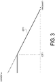
- the rated current changing unit 115 sets the rated current on the secondary side to a fixed value. For example, as shown in FIG. 3 , when the frequency of the carrier wave is higher than a current adjustment threshold value CT1, the rated current changing unit 115 calculates, based on an adjustment profile CP1 representing a relationship between the frequency of the carrier wave and the rated current on the secondary side, the rated current on the secondary side corresponding to the frequency of the carrier wave.
- the adjustment profile CP1 is defined so as to have the rated current on the secondary side decreasing in accordance with increase in the frequency of the carrier wave.
- the adjustment profile CP1 may be defined so as to have the rated current linearly decreasing with increase in the frequency of the carrier wave.
- power loss in each of the bidirectional switches 2RU, 2SU, 2TU, 2RV, 2SV, 2TV, 2RW, 2SW, and 2TW includes switching loss and steady loss.
- the switching loss is loss due to switching between the ON state and the OFF state.
- the steady loss is loss due to a current steadily flowing in the ON state.
- the bidirectional switches 2RU, 2SU, 2TU, 2RV, 2SV, 2TV, 2RW, 2SW, and 2TW are more frequently switched on and off, and thus the switching loss increases. Therefore, when the steady loss is constant, the power loss increases in accordance with increase in the frequency of the carrier wave. In this case, if the rated current on the secondary side is decreased in accordance with increase in the frequency of the carrier wave, the steady loss decreases in accordance with increase in the frequency of the carrier wave. Thus, increase in the power loss in accordance with increase in the frequency of the carrier wave can be reduced.
- the rated current changing unit 115 sets the rated current to the fixed value.
- the rated current changing unit 115 sets the rated current to a predetermined fixed current value, when the frequency of the carrier wave is lower than the current adjustment threshold value.
- the fixed current value may be a value of the rated current corresponding to the current adjustment threshold value in the adjustment profile CP1.
- the carrier wave changing unit 116 changes the frequency of the carrier wave based on a nearness level between the frequency on the primary side and the frequency on the secondary side.
- the carrier wave changing unit 116 may change the frequency of the carrier wave based on the nearness level between the frequency on the primary side included in the above-described voltage information on the primary side and the frequency of the above-described voltage command.
- a method for evaluating the nearness level is not particularly limited as long as the nearness level indicates a degree of nearness between the frequency on the primary side and the frequency of the voltage command.
- the carrier wave changing unit 116 may evaluate the nearness level based on the absolute value of the difference between the frequency on the primary side and the frequency of the voltage command.
- a variable range of the frequency on the secondary side provided by the power conversion control unit 114 includes a first frequency band including the same frequency as the frequency on the primary side, a second frequency band lower than the first frequency band, and a third frequency band higher than the first frequency band.
- a “particular band” means that the maximum value of the particular band is equal to or less than the minimum value of the other band.
- the particular band is higher than another of the bands means that the minimum value of the particular band is equal to or greater than the maximum value of the other band. The same applies hereinafter.
- the carrier wave changing unit 116 sets the frequency of the carrier wave to a first carrier frequency.
- the carrier wave changing unit 116 sets the frequency of the carrier wave to a second carrier frequency lower than the first carrier frequency.
- the carrier wave changing unit 116 may use, as the first carrier frequency, a value equal to or higher than the current adjustment threshold value described above, and may use, as the second carrier frequency, a value lower than the current adjustment threshold value.
- the carrier wave changing unit 116 may use, as the second carrier frequency, a value higher than the cutoff frequency of the filter 30.
- variable range of the frequency on the secondary side provided by the power conversion control unit 114 may further include a fourth frequency band lower than the second frequency band, and when the frequency on the secondary side is within the fourth frequency band, the carrier wave changing unit 116 may set the frequency of the carrier wave to the second carrier frequency.
- the carrier wave changing unit 116 may change the frequency of the carrier wave further based on the magnitude of the current on the secondary side.
- the variable range of the magnitude of the current on the secondary side provided by the power conversion control unit 114 may include a first current band and a second current band lower than the first current band.
- the carrier wave changing unit 116 may not perform changing the frequency of the carrier wave based on the nearness level, and when the magnitude of the current on the secondary side is within the first current band, the carrier wave changing unit 116 may perform changing the frequency of the carrier wave based on the nearness level. For example, when the magnitude of the current on the secondary side is within the second current band, the carrier wave changing unit 116 sets the frequency of the carrier wave to the first carrier frequency. When the magnitude of the current on the secondary side is within the first current band, the carrier wave changing unit 116 changes the frequency of the carrier wave depending on which of the first frequency band, the second frequency band, the third frequency band, and the fourth frequency band the frequency on the secondary side falls within.
- the carrier wave changing unit 116 sets the frequency of the carrier wave to the first carrier frequency, and when the frequency on the secondary side is within the first frequency band, or when the frequency on the secondary side is within the fourth frequency band, the carrier wave changing unit 116 sets the frequency of the carrier wave to the second carrier frequency.
- the variable range of the frequency on the secondary side provided by the power conversion control unit 114 includes a frequency band FR1 (a first frequency band) including a frequency F1 equal to the frequency on the primary side, a frequency band FR2 (a second frequency band) lower than the frequency band FR1, a frequency band FR3 (a third frequency band) higher than the frequency band FR1, and a frequency band FR4 (a fourth frequency band) lower than the frequency band FR2.
- FR1 a first frequency band
- F1 equal to the frequency on the primary side
- FR2 a second frequency band
- FR3 a third frequency band
- FR4 a fourth frequency band
- the minimum value of the frequency band FR1 is 85 to 95% of the frequency F1
- the maximum value of the frequency band FR1 is 105 to 110% of the frequency F1
- the minimum value of the frequency band FR4 is zero
- the maximum value of the frequency band FR4 is 5 to 15% of the frequency F1.
- the minimum value of the frequency band FR2 is equal to or greater than the maximum value of the frequency band FR4.
- the minimum value of the frequency band FR2 is more than the maximum value of the frequency band FR4, and a buffer band FR5 is interposed between the frequency band FR4 and the frequency band FR2.
- the maximum value of the frequency band FR2 is equal to or less than the minimum value of the frequency band FR1.
- the maximum value of the frequency band FR2 is less than the minimum value of the frequency band FR1, and a buffer band FR6 is interposed between the frequency band FR2 and the frequency band FR1.
- the minimum value of the frequency band FR3 is equal to or greater than the maximum value of the frequency band FR1.
- the minimum value of the frequency band FR3 is more than the maximum value of the frequency band FR1, and a buffer band FR7 is interposed between the frequency band FR1 and the frequency band FR3.
- the carrier wave changing unit 116 sets the frequency of the carrier wave to the first carrier frequency.
- the carrier wave changing unit 116 changes the frequency of the carrier wave depending on which of the frequency bands FR1, FR2, FR3, and FR4 the frequency on the secondary side falls within.
- the carrier wave changing unit 116 sets the frequency of the carrier wave to the first carrier frequency, and when the frequency on the secondary side is within the frequency band FR1, or when the frequency on the secondary side is within the frequency band FR4, the carrier wave changing unit 116 sets the frequency of the carrier wave to the second carrier frequency.
- the carrier wave changing unit 116 does not change the frequency of the carrier wave.
- the frequency of the carrier wave is changed depending on which of the frequency bands FR1, FR2, FR3, and FR4 the frequency on the secondary side falls within, and thus the current band AR1 is an example of the above-described first current band.
- the carrier wave changing unit 116 sets the frequency of the carrier wave to the first carrier frequency. In a case where the magnitude of the current on the secondary side is within the buffer band AR3, when the frequency on the secondary side is out of the frequency band FR2 and the frequency on the secondary side is out of the frequency band FR3, the carrier wave changing unit 116 does not change the frequency of the carrier wave.
- Examples of such a case include a case where, in a state where the frequency of the carrier wave is held at the second carrier frequency after the magnitude of the current on the secondary side was changed, when the frequency on the secondary side was within the frequency band FR4, from a value within the current band AR1 to a value within the buffer band AR3, the frequency on the secondary side is changed through the buffer band FR5 to a frequency within the frequency band FR2.
- the buffer band AR3 is also an example of the above-described first current band.
- the functional blocks described above are components of the control circuit 100, and thus processing executed by these functional blocks is equivalent to processing executed by the control circuit 100.
- FIG. 5 is a block diagram illustrating an example of a hardware configuration of the control circuit 100.
- the control circuit 100 includes one or more processors 191, a memory 192, a storage 193, a communication port 194, an I/O port 195, and a switch control circuit 196.
- the storage 193 includes a computer-readable storage medium such as a non-volatile semiconductor memory, for example.
- the storage 193 stores a program causing the power conversion device to execute switching on and off the plurality of switching elements of the matrix converter circuit in unison with the carrier wave to cause the alternating current on the secondary side of the matrix converter circuit to follow the control command, the matrix converter circuit being configured to perform bidirectional power conversion between the alternating current power on the primary side and the alternating current power on the secondary side, and changing, based on the nearness level between the frequency on the primary side and the frequency on the secondary side, the frequency of the carrier wave.
- the memory 192 temporarily stores programs loaded from the storage medium of the storage 193 and calculation results from the processor 191.
- the processor 191 implements each functional block of the control circuit 100 by executing the program described above in cooperation with the memory 192.
- the I/O port 195 inputs and outputs electric signals to and from the voltage detection circuit 40 and the current sensor 50 in accordance with commands from the processor 191.
- the communication port 194 performs information communication with the upper controller 200 in accordance with commands from the processor 191.
- the switch control circuit 196 outputs, to the matrix converter circuit 10, a drive signal for switching on and off the bidirectional switches 2RU, 2SU, 2TU, 2RV, 2SV, 2TV, 2RW, 2SW, and 2TW, in accordance with commands from the processor 191.
- control circuit 100 the functions are not limited to being implemented by a program.
- control circuit 100 may implement at least one function by a dedicated logic circuit or an application specific integrated circuit (ASIC) integrated therewith.
- ASIC application specific integrated circuit
- This procedure includes switching on and off the plurality of switching elements of the matrix converter circuit in unison with the carrier wave to cause the alternating current on the secondary side of the matrix converter circuit to follow the control command, the matrix converter circuit being configured to perform bidirectional power conversion between the alternating current power on the primary side and the alternating current power on the secondary side, and changing, based on the nearness level between the frequency on the primary side and the frequency on the secondary side, the frequency of the carrier wave.
- the control circuit 100 sequentially executes steps S01, S02, S03, S04, S05, S06, and S07.
- step S01 the current information acquisition unit 111 acquires current information of the power lines 12U, 12V, and 12W from the current sensor 50.
- step S02 the command generation unit 112 generates a voltage command based on a frequency command and the current information on the secondary side acquired by the current information acquisition unit 111.
- step S03 the phase and amplitude calculation unit 113 calculates, based on the phase voltages of the power lines 11R, 11S, and 11T acquired by the voltage detection circuit 40, the phase, amplitude, and frequency of the alternating current voltage on the primary side (the above-described voltage information on the primary side).
- step S04 the carrier wave changing unit 116 sets, based on the magnitude of the current on the secondary side and the frequency on the secondary side, the frequency of the carrier wave. The setting procedure of the frequency of the carrier wave will be described below.
- step S05 the rated current changing unit 115 sets the rated current on the secondary side, based on the frequency of the carrier wave set in step S04. For example, when the frequency of the carrier wave is lower than the above-described current adjustment threshold value, the rated current changing unit 115 sets, to the above-described fixed current value, the rated current on the secondary side. When the frequency of the carrier wave is higher than the current adjustment threshold value, the rated current changing unit 115 sets, based on the above-described adjustment profile CP1 and the frequency of the carrier wave, the rated current on the secondary side.
- the command generation unit 112 modifies the voltage command such that the magnitude of the current on the secondary side is limited to be equal to or less than the rated current.
- step S07 the power conversion control unit 114 starts to switch on and off the bidirectional switches 2RU, 2SU, 2TU, 2RV, 2SV, 2TV, 2RW, 2SW, and 2TW in unison with the carrier wave to cause the alternating current on the secondary side to follow the control command.
- the control circuit 100 repeats the procedure described above in predetermined control cycles.
- FIG. 7 is flowchart illustrating an example of a setting procedure of the frequency of the carrier wave in step S04.
- the control circuit 100 first executes step S11.
- step S11 the carrier wave changing unit 116 checks whether the magnitude of the current on the secondary side is within the current band AR2. In a case in which it is determined in step S11 that the magnitude of the current on the secondary side is within the current band AR2, the control circuit 100 executes step S12.
- step S12 the carrier wave changing unit 116 sets the frequency of the carrier wave to the above-described first carrier frequency.
- step S11 determines whether the magnitude of the current on the secondary side is within the current band AR2
- the control circuit 100 executes step S13.
- step S13 the carrier wave changing unit 116 checks whether the magnitude of the current on the secondary side is within the current band AR1.
- step S21 the carrier wave changing unit 116 checks whether the frequency on the secondary side is within the frequency band FR2. In a case in which it is determined in step S21 that the frequency on the secondary side is not within the frequency band FR2, the control circuit 100 executes step S22. In step S22, the carrier wave changing unit 116 checks whether the frequency on the secondary side is within the frequency band FR3.
- step S21 determines that the frequency on the secondary side is within the frequency band FR2
- step S22 determines that the frequency on the secondary side is within the frequency band FR3
- step S23 the carrier wave changing unit 116 sets the frequency of the carrier wave to the above-described first carrier frequency.
- step S24 the carrier wave changing unit 116 checks whether the frequency on the secondary side is within the frequency band FR1. In a case in which it is determined in step S24 that the frequency on the secondary side is not within the frequency band FR1, the control circuit 100 executes step S25. In step S25, the carrier wave changing unit 116 checks whether the frequency on the secondary side is within the frequency band FR4.
- step S24 the control circuit 100 executes step S26.
- step S26 the carrier wave changing unit 116 sets the frequency of the carrier wave to the above-described second carrier frequency.
- the carrier wave changing unit 116 does not perform changing the frequency of the carrier wave in accordance with the frequency on the secondary side.
- step S31 the carrier wave changing unit 116 checks whether the frequency on the secondary side is within the frequency band FR2. In a case in which it is determined in step S31 that the frequency on the secondary side is not within the frequency band FR2, the control circuit 100 executes step S32. In step S32, the carrier wave changing unit 116 checks whether the frequency on the secondary side is within the frequency band FR3.
- step S31 the control circuit 100 executes step S33.
- step S33 the carrier wave changing unit 116 sets the frequency of the carrier wave to the above-described first carrier frequency.
- step S32 the carrier wave changing unit 116 does not perform changing the frequency of the carrier wave in accordance with the frequency on the secondary side. At this point, the setting of the frequency of the carrier wave is completed.
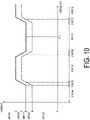
- FIG. 10 is a graph of a modified setting example of the frequency bands and the current bands, where the vertical axis indicates the magnitude of the current on the secondary side, and the horizontal axis indicates the frequency on the secondary side.
- the variable range of the current on the secondary side provided by the power conversion control unit 114 includes a current band AR11, a current band AR12 lower than the current band AR11, and a current band AR13 higher than the current band AR11.
- the minimum value of the current band AR11 is, for example, the rated current.
- the minimum value of the current band AR12 is zero, and the maximum value of the current band AR12 is equal to or less than the rated current.
- the maximum value of the current band AR12 is less than the minimum value of the current band AR11, and a buffer band AR14 is interposed between the current band AR11 and the current band AR12.
- the maximum value of the current band AR11 is, for example, 100 to 120% of the rated current.
- the minimum value of the current band AR13 is equal to or greater than the maximum value of the current band AR11.
- the minimum value of the current band AR13 is more than the maximum value of the current band AR11, and a buffer band AR15 is interposed between the current band AR11 and the current band AR13.
- the variable range of the frequency on the secondary side provided by the power conversion control unit 114 includes a frequency band FR11 (the first frequency band) including a frequency F1 equal to the frequency on the primary side, a frequency band FR12 (the second frequency band) lower than the frequency band FR11, a frequency band FR13 (the third frequency band) higher than the frequency band FR11, and a frequency band FR14 (the fourth frequency band) lower than the frequency band FR12.
- the minimum value of the frequency band FR11 is 85 to 95% of the frequency F1
- the maximum value of the frequency band FR11 is 105 to 110% of the frequency F1
- the minimum value of the frequency band FR14 is zero
- the maximum value of the frequency band FR14 is 5 to 15% of the frequency F1.
- the minimum value of the frequency band FR12 is equal to or greater than the maximum value of the frequency band FR14.
- the minimum value of the frequency band FR12 is more than the maximum value of the frequency band FR14, and a buffer band FR15 is interposed between the frequency band FR14 and the frequency band FR12.
- the maximum value of the frequency band FR12 is equal to or less than the minimum value of the frequency band FR11.
- the maximum value of the frequency band FR12 is less than the minimum value of the frequency band FR11, and a buffer band FR16 is interposed between the frequency band FR12 and the frequency band FR11.
- the minimum value of the frequency band FR13 is equal to or greater than the maximum value of the frequency band FR11.
- the minimum value of the frequency band FR13 is more than the maximum value of the frequency band FR11, and a buffer band FR17 is interposed between the frequency band FR11 and the frequency band FR13.
- the bandwidths of the frequency bands FR11, FR12, FR13, and FR14 may change depending on the magnitude of the current on the secondary side. For example, in FIG. 10 , in accordance with increase in the current on the secondary side, the bandwidths of the frequency bands FR11 and FR14 increase and the bandwidths of the frequency bands FR12 and FR13 decrease.
- the carrier wave changing unit 116 sets the frequency of the carrier wave to the first carrier frequency.
- the carrier wave changing unit 116 sets the frequency of the carrier wave to the second carrier frequency.
- the carrier wave changing unit 116 changes the frequency of the carrier wave depending on which of the frequency bands FR11, FR12, FR13, and FR14 the frequency on the secondary side falls within. For example, when the frequency on the secondary side is within the frequency band FR12, or when the frequency on the secondary side is within the frequency band FR13, the carrier wave changing unit 116 sets the frequency of the carrier wave to the first carrier frequency, and when the frequency on the secondary side is within the frequency band FR11, or when the frequency on the secondary side is within the frequency band FR14, the carrier wave changing unit 116 sets the frequency of the carrier wave to the second carrier frequency.
- the carrier wave changing unit 116 does not change the frequency of the carrier wave.
- the frequency of the carrier wave is changed depending on which of the frequency bands FR11, FR12, FR13, and FR14 the frequency on the secondary side falls within, and thus the current band AR11 is an example of the above-described first current band.
- the carrier wave changing unit 116 sets the frequency of the carrier wave to the first carrier frequency. In a case where the magnitude of the current on the secondary side is within the buffer band AR14, when the frequency on the secondary side is out of the frequency band FR12 and the frequency on the secondary side is out of the frequency band FR13, the carrier wave changing unit 116 does not change the frequency of the carrier wave.
- Examples of such a case include a case where, in a state where the frequency of the carrier wave is held at the second carrier frequency after the magnitude of the current on the secondary side was changed, when the frequency on the secondary side was within the frequency band FR14, from a value within the current band AR11 to a value within the buffer band AR14, the frequency on the secondary side is changed through the buffer band FR15 to a frequency within the frequency band FR12.
- the buffer band AR14 is also an example of the above-described first current band.
- the carrier wave changing unit 116 sets the frequency of the carrier wave to the second carrier frequency. In a case where the magnitude of the current on the secondary side is within the buffer band AR15, when the frequency on the secondary side is out of the frequency band FR11 and the frequency on the secondary side is out of the frequency band FR14, the carrier wave changing unit 116 does not change the frequency of the carrier wave.
- the buffer band AR15 is also an example of the above-described first current band.
- FIG. 11 is a flowchart illustrating an example of a setting procedure of the frequency of the carrier wave according to the example of FIG. 10 .
- the control circuit 100 first executes step S41.
- step S41 the carrier wave changing unit 116 checks whether the magnitude of the current on the secondary side is within the current band AR12. In a case in which it is determined in step S41 that the magnitude of the current on the secondary side is within the current band AR12, the control circuit 100 executes step S42.
- step S42 the carrier wave changing unit 116 sets the frequency of the carrier wave to the above-described first carrier frequency.
- step S43 the carrier wave changing unit 116 checks whether the magnitude of the current on the secondary side is within the current band AR13. In a case in which it is determined in step S43 that the magnitude of the current on the secondary side is within the current band AR13, the control circuit 100 executes step S44. In step S44, the carrier wave changing unit 116 sets the frequency of the carrier wave to the above-described second carrier frequency.
- step S43 the control circuit 100 executes step S45.
- step S45 the carrier wave changing unit 116 checks whether the magnitude of the current on the secondary side is within the current band AR11.
- step S51 the carrier wave changing unit 116 checks whether the frequency on the secondary side is within the frequency band FR12. In a case in which it is determined in step S51 that the frequency on the secondary side is not within the frequency band FR12, the control circuit 100 executes step S52. In step S52, the carrier wave changing unit 116 checks whether the frequency on the secondary side is within the frequency band FR13.
- step S51 determines that the frequency on the secondary side is within the frequency band FR12, or it is determined in step S52 that the frequency on the secondary side is within the frequency band FR13
- the control circuit 100 executes step S53.
- step S53 the carrier wave changing unit 116 sets the frequency of the carrier wave to the above-described first carrier frequency.
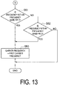
- step S54 the carrier wave changing unit 116 checks whether the frequency on the secondary side is within the frequency band FR11. In a case in which it is determined in step S54 that the frequency on the secondary side is not within the frequency band FR11, the control circuit 100 executes step S55. In step S55, the carrier wave changing unit 116 checks whether the frequency on the secondary side is within the frequency band FR14.
- step S54 determines that the frequency on the secondary side is within the frequency band FR11, or it is determined in step S55 that the frequency on the secondary side is within the frequency band FR14.
- step S56 the carrier wave changing unit 116 sets the frequency of the carrier wave to the above-described second carrier frequency.
- the carrier wave changing unit 116 does not perform changing the frequency of the carrier wave in accordance with the frequency on the secondary side.
- step S45 the control circuit 100 executes step S46.
- step S46 the carrier wave changing unit 116 checks whether the magnitude of the current on the secondary side is within the buffer band AR14.
- step S61 the carrier wave changing unit 116 checks whether the frequency on the secondary side is within the frequency band FR12. In a case in which it is determined in step S61 that the frequency on the secondary side is not within the frequency band FR12, the control circuit 100 executes step S62. In step S62, the carrier wave changing unit 116 checks whether the frequency on the secondary side is within the frequency band FR13.
- step S61 the control circuit 100 executes step S63.
- step S63 the carrier wave changing unit 116 sets the frequency of the carrier wave to the above-described first carrier frequency.
- the carrier wave changing unit 116 does not perform changing the frequency of the carrier wave in accordance with the frequency on the secondary side.
- step S71 the carrier wave changing unit 116 checks whether the frequency on the secondary side is within the frequency band FR11. In a case in which it is determined in step S71 that the frequency on the secondary side is not within the frequency band FR11, the control circuit 100 executes step S72. In step S72, the carrier wave changing unit 116 checks whether the frequency on the secondary side is within the frequency band FR14.
- step S71 In a case in which it is determined in step S71 that the frequency on the secondary side is within the frequency band FR11, or it is determined in step S72 that the frequency on the secondary side is within the frequency band FR14, the control circuit 100 executes step S73.
- step S73 the carrier wave changing unit 116 sets the frequency of the carrier wave to the above-described second carrier frequency.
- the carrier wave changing unit 116 does not perform changing the frequency of the carrier wave in accordance with the frequency on the secondary side. At this point, the setting of the frequency of the carrier wave is completed.
- the power conversion device 1 includes the matrix converter circuit 10 including the plurality of switching elements and being configured to perform bidirectional power conversion between the alternating current power on the primary side and the alternating current power on the secondary side, the power conversion control unit 114 configured to switch on and off the plurality of switching elements in unison with the carrier wave to cause the alternating current on the secondary side to follow the control command, and the carrier wave changing unit 116 configured to change, based on the nearness level between the frequency on the primary side and the frequency on the secondary side, the frequency of the carrier wave.
- Power loss in a switching element includes switching loss due to switching between the ON state and the OFF state, and steady loss due to a current steadily flowing in the ON state.
- the steady loss in each of the plurality of switching elements depends on a relationship upon switching to the ON state between the phase of the alternating current power on the primary side and the phase of the alternating current power on the secondary side.
- the frequency of the carrier wave can be changed based on the nearness level, for example, the frequency of the carrier wave can be decreased, when the nearness level is higher than the predetermined level. Decreasing the frequency of the carrier wave results in decrease in the switching loss, and thus even in a switching element having a large steady loss, the switching loss can be decreased and power loss and heat generation can be reduced. Accordingly, the present power conversion device 1 is effective in reducing heat generated by a switching element.
- the carrier wave changing unit 116 may change the frequency of the carrier wave further based on the magnitude of the current on the secondary side. Even in a state where the above-described nearness level is high, if the magnitude of the current on the secondary side is small, the quantity of heat generated in the switching element is small. Therefore, changing the frequency of the carrier wave further based on the magnitude of the current on the secondary side makes it possible to reduce the number of unnecessary changes of the frequency of the carrier wave.
- the variable range of the magnitude of the current on the secondary side provided by the power conversion control unit 114 may include the first current band and the second current band lower than the first current band, and when the magnitude of the current on the secondary side is within the second current band, the carrier wave changing unit 116 may not perform changing the frequency of the carrier wave based on the nearness level, and when the magnitude of the current on the secondary side is within the first current band, the carrier wave changing unit 116 may perform changing the frequency of the carrier wave based on the nearness level. In this case, changing the frequency of the carrier wave based on the nearness level is performed in a limited manner based on the magnitude of the current on the secondary side, and thus the number of unnecessary changes of the frequency of the carrier wave can be reduced.
- the variable range of the frequency on the secondary side provided by the power conversion control unit 114 includes the first frequency band including the same frequency as the frequency on the primary side, the second frequency band lower than the first frequency band, and the third frequency band higher than the first frequency band, and when the frequency on the secondary side is within the second frequency band, or when the frequency on the secondary side is within the third frequency band, the carrier wave changing unit 116 may set the frequency of the carrier wave to the first carrier frequency, and when the frequency on the secondary side is within the first frequency band, the carrier wave changing unit 116 may set the frequency of the carrier wave to the second carrier frequency lower than the first carrier frequency. In this case, changing the frequency of the carrier wave based on the nearness level can be realized with a simple logic.
- the variable range of the frequency on the secondary side provided by the power conversion control unit 114 may further include the fourth frequency band lower than the second frequency band, and when the frequency on the secondary side is within the fourth frequency band, the carrier wave changing unit 116 may set the frequency of the carrier wave to the second carrier frequency.
- a tuning frequency the same frequency as the frequency on the primary side
- a period during which the ON state or the OFF state of each of the switching elements is held becomes longer, and thus the quantity of heat generated in each of the switching elements may increase.
- the power conversion device 1 is more effective in reducing heat generated by a switching element.
- the power conversion device 1 may further include the filter 30 configured to reduce harmonics on the primary side, and the carrier wave changing unit 116 may use, as the second carrier frequency, a value higher than the cutoff frequency of the filter 30. In this case, it is possible to suppress increase in the ratio of high frequency components due to decreasing the frequency of the carrier wave.
- the power conversion device 1 may further include the rated current changing unit 115 configured to decrease the rated current on the secondary side in accordance with increase in the frequency of the carrier wave, when the frequency of the carrier wave is higher than the predetermined threshold value, and to set the rated current on the secondary side to a fixed value, when the frequency of the carrier wave is lower than the threshold value, the power conversion control unit 114 may switch on and off the plurality of switching elements based on the rated current on the secondary side to limit the magnitude of the current on the secondary side, and the carrier wave changing unit 116 may use, as the second carrier frequency, a value lower than the threshold value. In this case, decreasing the frequency of the carrier wave to a frequency within a band in which the rated current on the secondary side is held by the rated current changing unit 115 at the fixed value makes it possible to more reliably reduce power loss.
- the rated current changing unit 115 configured to decrease the rated current on the secondary side in accordance with increase in the frequency of the carrier wave, when the frequency of the carrier wave is higher than the
Landscapes
- Engineering & Computer Science (AREA)
- Power Engineering (AREA)
- Ac-Ac Conversion (AREA)
Abstract
Description
- The present disclosure relates to a power conversion device, a power conversion method, and a program.
- Patent Document 1 discloses a matrix converter including a plurality of bidirectional switches connecting phases of an alternating current power source and phases of an alternating current device. The matrix converter outputs electric power generated in the alternating current device to the alternating current power source and controls the alternating current device based on electric power supplied from the alternating current power source.
- Patent Document 1:
JP 2016-67169 A - The present disclosure provides a power conversion device effective in reducing heat generated in a switching element.
- A power conversion device according to an aspect of the present disclosure includes a matrix converter circuit including a plurality of switching elements and being configured to perform bidirectional power conversion between alternating current power on a primary side and alternating current power on a secondary side, a power conversion control unit configured to switch on and off the plurality of switching elements in unison with a carrier wave to cause an alternating current on the secondary side to follow a control command, and a carrier wave changing unit configured to change, based on a nearness level between a frequency on the primary side and a frequency on the secondary side, a frequency of the carrier wave.
- A power conversion method according to another aspect of the present disclosure includes switching on and off a plurality of switching elements of a matrix converter circuit in unison with a carrier wave to cause an alternating current on a secondary side of the matrix converter circuit to follow a control command, the matrix converter circuit being configured to perform bidirectional power conversion between alternating current power on a primary side and alternating current power on the secondary side, and changing, based on a nearness level between a frequency on the primary side and a frequency on the secondary side, a frequency of the carrier wave.
- A program according to still another aspect of the present disclosure causes a power conversion device to execute switching on and off a plurality of switching elements of a matrix converter circuit in unison with a carrier wave to cause an alternating current on a secondary side of the matrix converter circuit to follow a control command, the matrix converter circuit being configured to perform bidirectional power conversion between alternating current power on a primary side and alternating current power on the secondary side, and changing, based on a nearness level between a frequency on the primary side and a frequency on the secondary side, a frequency of the carrier wave.
- According to the present disclosure, it is possible to provide a power conversion device effective in reducing heat generated in a switching element.
-
-
FIG. 1 is a schematic diagram illustrating an example of a configuration of a power conversion device. -
FIG. 2 is a schematic view illustrating a specific example of a bidirectional switch. -
FIG. 3 is a graph of an example of a relationship between a frequency of a carrier wave and a rated current. -
FIG. 4 is a graph of a setting example of frequency bands and current bands. -
FIG. 5 is a block diagram illustrating an example of a hardware configuration of a control circuit. -
FIG. 6 is a flowchart illustrating an example of a control procedure of a matrix converter circuit. -
FIG. 7 is a flowchart illustrating an example of a setting procedure of the frequency of the carrier wave according toFIG. 4 . -
FIG. 8 is a flowchart illustrating an example of the setting procedure of the frequency of the carrier wave according toFIG. 4 . -
FIG. 9 is a flowchart illustrating an example of the setting procedure of the frequency of the carrier wave according toFIG. 4 . -
FIG. 10 is a graph of a modified example of the setting of frequency bands and current bands. -
FIG. 11 is a flowchart illustrating an example of a setting procedure of the frequency of the carrier wave according toFIG. 10 . -
FIG. 12 is a flowchart illustrating an example of the setting procedure of the frequency of the carrier wave according toFIG. 10 . -
FIG. 13 is a flowchart illustrating an example of the setting procedure of the frequency of the carrier wave according toFIG. 10 . -
FIG. 14 is a flowchart illustrating an example of the setting procedure of the frequency of the carrier wave according toFIG. 10 . - Embodiments will be described in detail below with reference to the drawings. In the description, elements which are the same or have the same function are given the same reference numbers, and redundant descriptions thereof are omitted.
- A power conversion device 1 illustrated in
FIG. 1 is a device that performs bidirectional power conversion between alternating current power on a primary side and alternating current power on a secondary side. For example, the power conversion device 1 converts the alternating current power on the primary side supplied from apower source 91 into the alternating current power on the secondary side and supplies the alternating current power on the secondary side to anelectric motor 92. Further, the power conversion device 1 converts the alternating current power on the secondary side generated by the electric motor 92 (regenerative power) into the alternating current power on the primary side and supplies the alternating current power on the primary side to thepower source 91. - The alternating current power on the primary side and the alternating current power on the secondary side may be single-phase alternating current power or may be three-phase alternating current power. In the following, a case in which the alternating current power on the primary side and the alternating current power on the secondary side are both three-phase alternating current power will be described. For example, the alternating current power on the primary side includes three phases referred to as an R phase, an S phase and a T phase, and the alternating current power on the secondary side includes three phases referred to as a U phase, a V phase, and a W phase.
- The power conversion device 1 includes a
matrix converter circuit 10, afilter 30, avoltage detection circuit 40, acurrent sensor 50, and acontrol circuit 100. - The
matrix converter circuit 10 includes a plurality of switching elements, and performs bidirectional power conversion between the alternating current power on the primary side and the alternating current power on the secondary side. In this bidirectional power conversion, conversion into a direct current is not involved. For example, thematrix converter circuit 10 includes power lines on theprimary side secondary side power line 11R is a transmission line for the R phase, thepower line 11S is a transmission line for the S phase, and thepower line 11T is a transmission line for the T phase. Thepower line 12U is a transmission line for the U phase, thepower line 12V is a transmission line for the V phase, and thepower line 12W is a transmission line for the W phase. - Each of the bidirectional switches 2RU, 2SU, 2TU, 2RV, 2SV, 2TV, 2RW, 2SW, and 2TW switches among three states, which are a state in which the switch allows a current to flow from the primary side to the secondary side, a state in which the switch allows a current to flow from the secondary side to the primary side, and a state in which the switch does not allow a current to flow. The bidirectional switch 2RU is interposed between the
power line 11R and thepower line 12U, and switches among a first ON state in which the bidirectional switch 2RU allows a current to flow from thepower line 11R to thepower line 12U, a second ON state in which the bidirectional switch 2RU allows a current to flow from thepower line 12U to thepower line 11R, and a bidirectional OFF state in which the bidirectional switch 2RU does not allow a current to flow. The bidirectional switch 2SU is interposed between thepower line 11S and thepower line 12U, and switches among a first ON state in which the bidirectional switch 2SU allows a current to flow from thepower line 11S to thepower line 12U, a second ON state in which the bidirectional switch 2SU allows a current to flow from thepower line 12U to thepower line 11S, and a bidirectional OFF state in which the bidirectional switch 2SU does not allow a current to flow. The bidirectional switch 2TU is interposed between thepower line 11T and thepower line 12U, and switches among a first ON state in which the bidirectional switch 2TU allows a current to flow from thepower line 11T to thepower line 12U, a second ON state in which the bidirectional switch 2TU allows a current to flow from thepower line 12U to thepower line 11T, and a bidirectional OFF state in which the bidirectional switch 2TU does not allow a current to flow. - The bidirectional switch 2RV is interposed between the
power line 11R and thepower line 12V, and switches among a first ON state in which the bidirectional switch 2RV allows a current to flow from thepower line 11R to thepower line 12V, a second ON state in which the bidirectional switch 2RV allows a current to flow from thepower line 12V to thepower line 11R, and a bidirectional OFF state in which the bidirectional switch 2RV does not allow a current to flow. The bidirectional switch 2SV is interposed between thepower line 11S and thepower line 12V, and switches among a first ON state in which the bidirectional switch 2SV allows a current to flow from thepower line 11S to thepower line 12V, a second ON state in which the bidirectional switch 2SV allows a current to flow from thepower line 12V to thepower line 11S, and a bidirectional OFF state in which the bidirectional switch 2SV does not allow a current to flow. The bidirectional switch 2TV is interposed between thepower line 11T and thepower line 12V, and switches among a first ON state in which the bidirectional switch 2TV allows a current to flow from thepower line 11T to thepower line 12V, a second ON state in which the bidirectional switch 2TV allows a current to flow from thepower line 12V to thepower line 11T, and a bidirectional OFF state in which the bidirectional switch 2TV does not allow a current to flow. - The bidirectional switch 2RW is interposed between the
power line 11R and thepower line 12W, and switches among a first ON state in which the bidirectional switch 2RW allows a current to flow from thepower line 11R to thepower line 12W, a second ON state in which the bidirectional switch 2RW allows a current to flow from thepower line 12W to thepower line 11R, and a bidirectional OFF state in which the bidirectional switch 2RW does not allow a current to flow. The bidirectional switch 2SW is interposed between thepower line 11S and thepower line 12W, and switches among a first ON state in which the bidirectional switch 2SW allows a current to flow from thepower line 11S to thepower line 12W, a second ON state in which the bidirectional switch 2SW allows a current to flow from thepower line 12W to thepower line 11S, and a bidirectional OFF state in which the bidirectional switch 2SW does not allow a current to flow. The bidirectional switch 2TW is interposed between thepower line 11T and thepower line 12W, and switches among a first ON state in which the bidirectional switch 2TW allows a current to flow from thepower line 11T to thepower line 12W, a second ON state in which the bidirectional switch 2TW allows a current to flow from thepower line 12W to thepower line 11T, and a bidirectional OFF state in which the bidirectional switch 2TW does not allow a current to flow. - As illustrated in
FIG. 2 , each of the bidirectional switches 2RU, 2SU, 2TU, 2RV, 2SV, 2TV, 2RW, 2SW, and 2TW has twoswitches 21 and 22. Theswitch 21 in an ON state allows a current to flow from the primary side to the secondary side and does not allow a current to flow from the secondary side to the primary side. The switch 22 in an ON state allows a current to flow from the secondary side to the primary side and does not allow a current to flow from the primary side to the secondary side. In each of the bidirectional switches 2RU, 2SU, 2TU, 2RV, 2SV, 2TV, 2RW, 2SW, and 2TW, the above-described first ON state is a state where theswitch 21 is in the ON state and the switch 22 is in the OFF state, the above-described second ON state is a state where theswitch 21 is in the OFF state and the switch 22 is in the ON state, and the above-described bidirectional OFF state is a state where theswitches 21 and 22 are in an OFF state. - Returning to
FIG. 1 , thefilter 30 reduces harmonics in the alternating current power on the primary side. For example, thefilter 30 includesinductors capacitors inductors power lines capacitor 34R is provided on the secondary side of theinductor 31R (between theinductor 31R and the bidirectional switches 2RU, 2RV, and 2RW) and between thepower line 11R and aneutral point 35. Thecapacitor 34S is provided on the secondary side of theinductor 31S (between theinductor 31S and the bidirectional switches 2SU, 2SV, and 2SW) and between thepower line 11S and theneutral point 35. Thecapacitor 34T is provided on the secondary side of theinductor 31T (between theinductor 31T and the bidirectional switches 2TU, 2TV, and 2TW) and between thepower line 11T and theneutral point 35. Thevoltage detection circuit 40 detects an alternating current voltage on the primary side. For example, thevoltage detection circuit 40 detects a phase voltage of each of thepower lines - The
current sensor 50 detects the magnitude of the current on the secondary side (the current flowing between thematrix converter circuit 10 and the electric motor 92). For example, thecurrent sensor 50 detects the magnitude of currents of thepower lines current sensor 50 may be configured to detect the magnitude of the currents for all of thepower lines power lines - The
control circuit 100 executes switching on and off the bidirectional switches 2RU, 2SU, 2TU, 2RV, 2SV, 2TV, 2RW, 2SW, and 2TW in unison with a carrier wave to cause the alternating current on the secondary side to follow a control command, and changing, based on a nearness level between a frequency on the primary side (the frequency of the alternating current on the primary side) and a frequency on the secondary side (the frequency of the alternating current on the secondary side), a frequency of the carrier wave. Causing the alternating current on the secondary side to follow the control command means causing a physical quantity relating to an electrical state of the alternating current power on the secondary side to follow the control command. Examples of the physical quantity relating to an electrical state include power, voltage, and current. The frequency of the alternating current means the frequency of the alternating current voltage or the frequency of the alternating current. - Specific examples of the control command include a voltage command. When the control command is a voltage command, the
control circuit 100 switches on and off the bidirectional switches 2RU, 2SU, 2TU, 2RV, 2SV, 2TV, 2RW, 2SW, and 2TW to cause the alternating current voltage on the secondary side to follow the voltage command. - For example, the
control circuit 100 includes, as functional components (hereinafter, referred to as "functional blocks"), a currentinformation acquisition unit 111, acommand generation unit 112, a phase andamplitude calculation unit 113, a powerconversion control unit 114, a rated current changingunit 115, and a carrierwave changing unit 116. The currentinformation acquisition unit 111 acquires current information of thepower lines current sensor 50. - The
command generation unit 112 generates a voltage command based on a frequency command and current information on the secondary side acquired by the currentinformation acquisition unit 111. Thecommand generation unit 112 acquires the frequency command from anupper controller 200, for example. Specific examples of theupper controller 200 include a programmable logic controller. For example, thecommand generation unit 112 calculates the voltage command such that operating speed of the electric motor 92 (for example, rotational speed) follows the frequency command. - The phase and
amplitude calculation unit 113 calculates the phase, amplitude, and frequency of the alternating current voltage on the primary side, based on the phase voltages of thepower lines voltage detection circuit 40. Hereinafter, the calculation results of the phase, amplitude, and frequency are referred to as "voltage information on the primary side". The powerconversion control unit 114 switches on and off the bidirectional switches 2RU, 2SU, 2TU, 2RV, 2SV, 2TV, 2RW, 2SW, and 2TW in unison with the carrier wave to cause the alternating current on the secondary side to follow the control command. For example, based on the voltage information on the primary side and the voltage command, the powerconversion control unit 114 switches on and off the bidirectional switches 2RU, 2SU, 2TU, 2RV, 2SV, 2TV, 2RW, 2SW, and 2TW in unison with the carrier wave to cause the alternating current voltage on the secondary side to follow the voltage command. - The power
conversion control unit 114 may switch on and off the bidirectional switches 2RU, 2SU, 2TU, 2RV, 2SV, 2TV, 2RW, 2SW, and 2TW based on a rated current on the secondary side so as to limit the magnitude of the current on the secondary side. For example, thecommand generation unit 112 may generate the voltage command such that the magnitude of the current on the secondary side is limited to be equal to or less than a current limit value determined based on the rated current. When the voltage command is generated in this way, the powerconversion control unit 114 switches on and off the bidirectional switches 2RU, 2SU, 2TU, 2RV, 2SV, 2TV, 2RW, 2SW, and 2TW such that the magnitude of the current on the secondary side is limited to be equal to or less than the current limit value. In this case, the powerconversion control unit 114 switches on and off the bidirectional switches 2RU, 2SU, 2TU, 2RV, 2SV, 2TV, 2RW, 2SW, and 2TW such that the bidirectional switches 2RU, 2SU, 2TU, 2RV, 2SV, 2TV, 2RW, 2SW, and 2TW have ON times which give a magnitude of the current equal to or less than the current limit value. - When the frequency of the carrier wave is higher than a predetermined threshold value (hereinafter, referred to as a "current adjustment threshold value"), the rated current changing
unit 115 decreases the rated current on the secondary side in accordance with increase in the frequency of the carrier wave. When the frequency of the carrier wave is lower than the current adjustment threshold value, the rated current changingunit 115 sets the rated current on the secondary side to a fixed value. For example, as shown inFIG. 3 , when the frequency of the carrier wave is higher than a current adjustment threshold value CT1, the rated current changingunit 115 calculates, based on an adjustment profile CP1 representing a relationship between the frequency of the carrier wave and the rated current on the secondary side, the rated current on the secondary side corresponding to the frequency of the carrier wave. The adjustment profile CP1 is defined so as to have the rated current on the secondary side decreasing in accordance with increase in the frequency of the carrier wave. In an example, the adjustment profile CP1 may be defined so as to have the rated current linearly decreasing with increase in the frequency of the carrier wave. - Here, power loss in each of the bidirectional switches 2RU, 2SU, 2TU, 2RV, 2SV, 2TV, 2RW, 2SW, and 2TW includes switching loss and steady loss. The switching loss is loss due to switching between the ON state and the OFF state. The steady loss is loss due to a current steadily flowing in the ON state.
- When the frequency of the carrier wave is increased, the bidirectional switches 2RU, 2SU, 2TU, 2RV, 2SV, 2TV, 2RW, 2SW, and 2TW are more frequently switched on and off, and thus the switching loss increases. Therefore, when the steady loss is constant, the power loss increases in accordance with increase in the frequency of the carrier wave. In this case, if the rated current on the secondary side is decreased in accordance with increase in the frequency of the carrier wave, the steady loss decreases in accordance with increase in the frequency of the carrier wave. Thus, increase in the power loss in accordance with increase in the frequency of the carrier wave can be reduced.
- As described above, when the frequency of the carrier wave is lower than the current adjustment threshold value, the rated current changing
unit 115 sets the rated current to the fixed value. For example, the rated current changingunit 115 sets the rated current to a predetermined fixed current value, when the frequency of the carrier wave is lower than the current adjustment threshold value. The fixed current value may be a value of the rated current corresponding to the current adjustment threshold value in the adjustment profile CP1. - Returning to
FIG. 1 , the carrierwave changing unit 116 changes the frequency of the carrier wave based on a nearness level between the frequency on the primary side and the frequency on the secondary side. For example, the carrierwave changing unit 116 may change the frequency of the carrier wave based on the nearness level between the frequency on the primary side included in the above-described voltage information on the primary side and the frequency of the above-described voltage command. A method for evaluating the nearness level is not particularly limited as long as the nearness level indicates a degree of nearness between the frequency on the primary side and the frequency of the voltage command. For example, the carrierwave changing unit 116 may evaluate the nearness level based on the absolute value of the difference between the frequency on the primary side and the frequency of the voltage command. - In an example, a variable range of the frequency on the secondary side provided by the power
conversion control unit 114 includes a first frequency band including the same frequency as the frequency on the primary side, a second frequency band lower than the first frequency band, and a third frequency band higher than the first frequency band. Here, that "one of bands (hereinafter, referred to as a "particular band") is lower than another of the bands" means that the maximum value of the particular band is equal to or less than the minimum value of the other band. That "the particular band is higher than another of the bands" means that the minimum value of the particular band is equal to or greater than the maximum value of the other band. The same applies hereinafter. - When the frequency on the secondary side is within the second frequency band, or when the frequency on the secondary side is within the third frequency band, the carrier
wave changing unit 116 sets the frequency of the carrier wave to a first carrier frequency. When the frequency on the secondary side is within the first frequency band, the carrierwave changing unit 116 sets the frequency of the carrier wave to a second carrier frequency lower than the first carrier frequency. - The carrier
wave changing unit 116 may use, as the first carrier frequency, a value equal to or higher than the current adjustment threshold value described above, and may use, as the second carrier frequency, a value lower than the current adjustment threshold value. The carrierwave changing unit 116 may use, as the second carrier frequency, a value higher than the cutoff frequency of thefilter 30. - The variable range of the frequency on the secondary side provided by the power
conversion control unit 114 may further include a fourth frequency band lower than the second frequency band, and when the frequency on the secondary side is within the fourth frequency band, the carrierwave changing unit 116 may set the frequency of the carrier wave to the second carrier frequency. - The carrier
wave changing unit 116 may change the frequency of the carrier wave further based on the magnitude of the current on the secondary side. In an example, the variable range of the magnitude of the current on the secondary side provided by the powerconversion control unit 114 may include a first current band and a second current band lower than the first current band. - When the magnitude of the current on the secondary side is within the second current band, the carrier
wave changing unit 116 may not perform changing the frequency of the carrier wave based on the nearness level, and when the magnitude of the current on the secondary side is within the first current band, the carrierwave changing unit 116 may perform changing the frequency of the carrier wave based on the nearness level. For example, when the magnitude of the current on the secondary side is within the second current band, the carrierwave changing unit 116 sets the frequency of the carrier wave to the first carrier frequency. When the magnitude of the current on the secondary side is within the first current band, the carrierwave changing unit 116 changes the frequency of the carrier wave depending on which of the first frequency band, the second frequency band, the third frequency band, and the fourth frequency band the frequency on the secondary side falls within. For example, when the frequency on the secondary side is within the second frequency band, or when the frequency on the secondary side is within the third frequency band, the carrierwave changing unit 116 sets the frequency of the carrier wave to the first carrier frequency, and when the frequency on the secondary side is within the first frequency band, or when the frequency on the secondary side is within the fourth frequency band, the carrierwave changing unit 116 sets the frequency of the carrier wave to the second carrier frequency. -
FIG. 4 is a graph of a setting example of the frequency bands and the current bands, where the vertical axis indicates the magnitude of the current on the secondary side, and the horizontal axis indicates the frequency on the secondary side. InFIG. 4 , the variable range of the magnitude of the current on the secondary side provided by the powerconversion control unit 114 includes a current band AR1 and a current band AR2 lower than the current band AR1. The minimum value of the current band AR1 is, for example, the rated current. The minimum value of the current band AR2 is zero, and the maximum value of the current band AR2 is equal to or less than the rated current. For example, the maximum value of the current band AR2 is less than the minimum value of the current band AR1, and a buffer band AR3 is interposed between the current band AR1 and the current band AR2. - The variable range of the frequency on the secondary side provided by the power
conversion control unit 114 includes a frequency band FR1 (a first frequency band) including a frequency F1 equal to the frequency on the primary side, a frequency band FR2 (a second frequency band) lower than the frequency band FR1, a frequency band FR3 (a third frequency band) higher than the frequency band FR1, and a frequency band FR4 (a fourth frequency band) lower than the frequency band FR2. - For example, the minimum value of the frequency band FR1 is 85 to 95% of the frequency F1, the maximum value of the frequency band FR1 is 105 to 110% of the frequency F1, the minimum value of the frequency band FR4 is zero, and the maximum value of the frequency band FR4 is 5 to 15% of the frequency F1. The minimum value of the frequency band FR2 is equal to or greater than the maximum value of the frequency band FR4. For example, the minimum value of the frequency band FR2 is more than the maximum value of the frequency band FR4, and a buffer band FR5 is interposed between the frequency band FR4 and the frequency band FR2. The maximum value of the frequency band FR2 is equal to or less than the minimum value of the frequency band FR1. For example, the maximum value of the frequency band FR2 is less than the minimum value of the frequency band FR1, and a buffer band FR6 is interposed between the frequency band FR2 and the frequency band FR1. The minimum value of the frequency band FR3 is equal to or greater than the maximum value of the frequency band FR1. For example, the minimum value of the frequency band FR3 is more than the maximum value of the frequency band FR1, and a buffer band FR7 is interposed between the frequency band FR1 and the frequency band FR3.
- In the example of
FIG. 4 , when the magnitude of the current on the secondary side is within the current band AR2, the carrierwave changing unit 116 sets the frequency of the carrier wave to the first carrier frequency. When the magnitude of the current on the secondary side is within the current band AR1, the carrierwave changing unit 116 changes the frequency of the carrier wave depending on which of the frequency bands FR1, FR2, FR3, and FR4 the frequency on the secondary side falls within. For example, when the frequency on the secondary side is within the frequency band FR2, or when the frequency on the secondary side is within the frequency band FR3, the carrierwave changing unit 116 sets the frequency of the carrier wave to the first carrier frequency, and when the frequency on the secondary side is within the frequency band FR1, or when the frequency on the secondary side is within the frequency band FR4, the carrierwave changing unit 116 sets the frequency of the carrier wave to the second carrier frequency. When the frequency on the secondary side is within the buffer band FR5, or when the frequency on the secondary side is within the buffer band FR6, or when the frequency on the secondary side is within the buffer band FR7, the carrierwave changing unit 116 does not change the frequency of the carrier wave. - As described above, when the magnitude of the current on the secondary side is within the current band AR1, the frequency of the carrier wave is changed depending on which of the frequency bands FR1, FR2, FR3, and FR4 the frequency on the secondary side falls within, and thus the current band AR1 is an example of the above-described first current band.
- In a case where the magnitude of the current on the secondary side is within the buffer band AR3, when the frequency on the secondary side is within the frequency band FR2, or when the frequency on the secondary side is within the frequency band FR3, the carrier
wave changing unit 116 sets the frequency of the carrier wave to the first carrier frequency. In a case where the magnitude of the current on the secondary side is within the buffer band AR3, when the frequency on the secondary side is out of the frequency band FR2 and the frequency on the secondary side is out of the frequency band FR3, the carrierwave changing unit 116 does not change the frequency of the carrier wave. In the case where the magnitude of the current on the secondary side is within the buffer band AR3, changing the frequency of the carrier wave from the first carrier frequency to the second carrier frequency does not occur, because, in this case, the frequency of the carrier wave is not changed, even when the frequency on the secondary side is within the frequency band FR1 or FR4. On the other hand, when the frequency on the secondary side falls within the frequency band FR2 or FR3, the frequency of the carrier wave may be changed from the second carrier frequency to the first carrier frequency. Examples of such a case include a case where, in a state where the frequency of the carrier wave is held at the second carrier frequency after the magnitude of the current on the secondary side was changed, when the frequency on the secondary side was within the frequency band FR4, from a value within the current band AR1 to a value within the buffer band AR3, the frequency on the secondary side is changed through the buffer band FR5 to a frequency within the frequency band FR2. Thus, the buffer band AR3 is also an example of the above-described first current band. - The functional blocks described above are components of the
control circuit 100, and thus processing executed by these functional blocks is equivalent to processing executed by thecontrol circuit 100. -
FIG. 5 is a block diagram illustrating an example of a hardware configuration of thecontrol circuit 100. As illustrated inFIG. 5 , thecontrol circuit 100 includes one ormore processors 191, amemory 192, astorage 193, acommunication port 194, an I/O port 195, and aswitch control circuit 196. Thestorage 193 includes a computer-readable storage medium such as a non-volatile semiconductor memory, for example. Thestorage 193 stores a program causing the power conversion device to execute switching on and off the plurality of switching elements of the matrix converter circuit in unison with the carrier wave to cause the alternating current on the secondary side of the matrix converter circuit to follow the control command, the matrix converter circuit being configured to perform bidirectional power conversion between the alternating current power on the primary side and the alternating current power on the secondary side, and changing, based on the nearness level between the frequency on the primary side and the frequency on the secondary side, the frequency of the carrier wave. Thememory 192 temporarily stores programs loaded from the storage medium of thestorage 193 and calculation results from theprocessor 191. Theprocessor 191 implements each functional block of thecontrol circuit 100 by executing the program described above in cooperation with thememory 192. The I/O port 195 inputs and outputs electric signals to and from thevoltage detection circuit 40 and thecurrent sensor 50 in accordance with commands from theprocessor 191. Thecommunication port 194 performs information communication with theupper controller 200 in accordance with commands from theprocessor 191. Theswitch control circuit 196 outputs, to thematrix converter circuit 10, a drive signal for switching on and off the bidirectional switches 2RU, 2SU, 2TU, 2RV, 2SV, 2TV, 2RW, 2SW, and 2TW, in accordance with commands from theprocessor 191. - Note that in the
control circuit 100, the functions are not limited to being implemented by a program. For example, thecontrol circuit 100 may implement at least one function by a dedicated logic circuit or an application specific integrated circuit (ASIC) integrated therewith. - Next, as an example of the power conversion method, an example of a control procedure of the
matrix converter circuit 10 executed by thecontrol circuit 100 will be described. This procedure includes switching on and off the plurality of switching elements of the matrix converter circuit in unison with the carrier wave to cause the alternating current on the secondary side of the matrix converter circuit to follow the control command, the matrix converter circuit being configured to perform bidirectional power conversion between the alternating current power on the primary side and the alternating current power on the secondary side, and changing, based on the nearness level between the frequency on the primary side and the frequency on the secondary side, the frequency of the carrier wave. - As illustrated in
FIG. 6 , thecontrol circuit 100 sequentially executes steps S01, S02, S03, S04, S05, S06, and S07. In step S01, the currentinformation acquisition unit 111 acquires current information of thepower lines current sensor 50. In step S02, thecommand generation unit 112 generates a voltage command based on a frequency command and the current information on the secondary side acquired by the currentinformation acquisition unit 111. - In step S03, the phase and
amplitude calculation unit 113 calculates, based on the phase voltages of thepower lines voltage detection circuit 40, the phase, amplitude, and frequency of the alternating current voltage on the primary side (the above-described voltage information on the primary side). In step S04, the carrierwave changing unit 116 sets, based on the magnitude of the current on the secondary side and the frequency on the secondary side, the frequency of the carrier wave. The setting procedure of the frequency of the carrier wave will be described below. - In step S05, the rated current changing
unit 115 sets the rated current on the secondary side, based on the frequency of the carrier wave set in step S04. For example, when the frequency of the carrier wave is lower than the above-described current adjustment threshold value, the rated current changingunit 115 sets, to the above-described fixed current value, the rated current on the secondary side. When the frequency of the carrier wave is higher than the current adjustment threshold value, the rated current changingunit 115 sets, based on the above-described adjustment profile CP1 and the frequency of the carrier wave, the rated current on the secondary side. In step S06, thecommand generation unit 112 modifies the voltage command such that the magnitude of the current on the secondary side is limited to be equal to or less than the rated current. In step S07, the powerconversion control unit 114 starts to switch on and off the bidirectional switches 2RU, 2SU, 2TU, 2RV, 2SV, 2TV, 2RW, 2SW, and 2TW in unison with the carrier wave to cause the alternating current on the secondary side to follow the control command. Thecontrol circuit 100 repeats the procedure described above in predetermined control cycles. -
FIG. 7 is flowchart illustrating an example of a setting procedure of the frequency of the carrier wave in step S04. As illustrated inFIG. 7 , thecontrol circuit 100 first executes step S11. In step S11, the carrierwave changing unit 116 checks whether the magnitude of the current on the secondary side is within the current band AR2. In a case in which it is determined in step S11 that the magnitude of the current on the secondary side is within the current band AR2, thecontrol circuit 100 executes step S12. In step S12, the carrierwave changing unit 116 sets the frequency of the carrier wave to the above-described first carrier frequency. - In a case in which it is determined in step S11 that the magnitude of the current on the secondary side is not within the current band AR2, the
control circuit 100 executes step S13. In step S13, the carrierwave changing unit 116 checks whether the magnitude of the current on the secondary side is within the current band AR1. - In a case in which it is determined in step S13 that the magnitude of the current on the secondary side is within the current band AR1, the
control circuit 100 executes step S21, as illustrated inFIG. 8 . In step S21, the carrierwave changing unit 116 checks whether the frequency on the secondary side is within the frequency band FR2. In a case in which it is determined in step S21 that the frequency on the secondary side is not within the frequency band FR2, thecontrol circuit 100 executes step S22. In step S22, the carrierwave changing unit 116 checks whether the frequency on the secondary side is within the frequency band FR3. In a case in which it is determined in step S21 that the frequency on the secondary side is within the frequency band FR2, or it is determined in step S22 that the frequency on the secondary side is within the frequency band FR3, thecontrol circuit 100 executes step S23. In step S23, the carrierwave changing unit 116 sets the frequency of the carrier wave to the above-described first carrier frequency. - In a case in which it is determined in step S22 that the frequency on the secondary side is not within the frequency band FR3, the
control circuit 100 executes step S24. In step S24, the carrierwave changing unit 116 checks whether the frequency on the secondary side is within the frequency band FR1. In a case in which it is determined in step S24 that the frequency on the secondary side is not within the frequency band FR1, thecontrol circuit 100 executes step S25. In step S25, the carrierwave changing unit 116 checks whether the frequency on the secondary side is within the frequency band FR4. In a case in which it is determined in step S24 that the frequency on the secondary side is within the frequency band FR1, or it is determined in step S25 that the frequency on the secondary side is within the frequency band FR4, thecontrol circuit 100 executes step S26. In step S26, the carrierwave changing unit 116 sets the frequency of the carrier wave to the above-described second carrier frequency. - In a case in which it is determined in step S25 that the frequency on the secondary side is not within the frequency band FR4, the carrier
wave changing unit 116 does not perform changing the frequency of the carrier wave in accordance with the frequency on the secondary side. - In a case in which it is determined in step S13 (see
FIG. 7 ) that the magnitude of the current on the secondary side is not within the current band AR1, thecontrol circuit 100 executes step S31, as illustrated inFIG. 9 . In step S31, the carrierwave changing unit 116 checks whether the frequency on the secondary side is within the frequency band FR2. In a case in which it is determined in step S31 that the frequency on the secondary side is not within the frequency band FR2, thecontrol circuit 100 executes step S32. In step S32, the carrierwave changing unit 116 checks whether the frequency on the secondary side is within the frequency band FR3. In a case in which it is determined in step S31 that the frequency on the secondary side is within the frequency band FR2, or it is determined in step S32 that the frequency on the secondary side is within the frequency band FR3, thecontrol circuit 100 executes step S33. In step S33, the carrierwave changing unit 116 sets the frequency of the carrier wave to the above-described first carrier frequency. - In a case in which it is determined in step S32 that the frequency on the secondary side is not within the frequency band FR3, the carrier
wave changing unit 116 does not perform changing the frequency of the carrier wave in accordance with the frequency on the secondary side. At this point, the setting of the frequency of the carrier wave is completed. -
FIG. 10 is a graph of a modified setting example of the frequency bands and the current bands, where the vertical axis indicates the magnitude of the current on the secondary side, and the horizontal axis indicates the frequency on the secondary side. InFIG. 10 , the variable range of the current on the secondary side provided by the powerconversion control unit 114 includes a current band AR11, a current band AR12 lower than the current band AR11, and a current band AR13 higher than the current band AR11. - The minimum value of the current band AR11 is, for example, the rated current. The minimum value of the current band AR12 is zero, and the maximum value of the current band AR12 is equal to or less than the rated current. For example, the maximum value of the current band AR12 is less than the minimum value of the current band AR11, and a buffer band AR14 is interposed between the current band AR11 and the current band AR12.
- The maximum value of the current band AR11 is, for example, 100 to 120% of the rated current. The minimum value of the current band AR13 is equal to or greater than the maximum value of the current band AR11. For example, the minimum value of the current band AR13 is more than the maximum value of the current band AR11, and a buffer band AR15 is interposed between the current band AR11 and the current band AR13.
- The variable range of the frequency on the secondary side provided by the power
conversion control unit 114 includes a frequency band FR11 (the first frequency band) including a frequency F1 equal to the frequency on the primary side, a frequency band FR12 (the second frequency band) lower than the frequency band FR11, a frequency band FR13 (the third frequency band) higher than the frequency band FR11, and a frequency band FR14 (the fourth frequency band) lower than the frequency band FR12. For example, the minimum value of the frequency band FR11 is 85 to 95% of the frequency F1, the maximum value of the frequency band FR11 is 105 to 110% of the frequency F1, the minimum value of the frequency band FR14 is zero, and the maximum value of the frequency band FR14 is 5 to 15% of the frequency F1. - The minimum value of the frequency band FR12 is equal to or greater than the maximum value of the frequency band FR14. For example, the minimum value of the frequency band FR12 is more than the maximum value of the frequency band FR14, and a buffer band FR15 is interposed between the frequency band FR14 and the frequency band FR12. The maximum value of the frequency band FR12 is equal to or less than the minimum value of the frequency band FR11. For example, the maximum value of the frequency band FR12 is less than the minimum value of the frequency band FR11, and a buffer band FR16 is interposed between the frequency band FR12 and the frequency band FR11. The minimum value of the frequency band FR13 is equal to or greater than the maximum value of the frequency band FR11. For example, the minimum value of the frequency band FR13 is more than the maximum value of the frequency band FR11, and a buffer band FR17 is interposed between the frequency band FR11 and the frequency band FR13.
- The bandwidths of the frequency bands FR11, FR12, FR13, and FR14 may change depending on the magnitude of the current on the secondary side. For example, in
FIG. 10 , in accordance with increase in the current on the secondary side, the bandwidths of the frequency bands FR11 and FR14 increase and the bandwidths of the frequency bands FR12 and FR13 decrease. - In the example of
FIG. 10 , when the magnitude of the current on the secondary side is within the current band AR12, the carrierwave changing unit 116 sets the frequency of the carrier wave to the first carrier frequency. When the magnitude of the current on the secondary side is within the current band AR13, the carrierwave changing unit 116 sets the frequency of the carrier wave to the second carrier frequency. - When the magnitude of the current on the secondary side is within the current band AR11, the carrier
wave changing unit 116 changes the frequency of the carrier wave depending on which of the frequency bands FR11, FR12, FR13, and FR14 the frequency on the secondary side falls within. For example, when the frequency on the secondary side is within the frequency band FR12, or when the frequency on the secondary side is within the frequency band FR13, the carrierwave changing unit 116 sets the frequency of the carrier wave to the first carrier frequency, and when the frequency on the secondary side is within the frequency band FR11, or when the frequency on the secondary side is within the frequency band FR14, the carrierwave changing unit 116 sets the frequency of the carrier wave to the second carrier frequency. - When the frequency on the secondary side is within the buffer band FR15, or when the frequency on the secondary side is within the buffer band FR16, or when the frequency on the secondary side is within the buffer band FR17, the carrier
wave changing unit 116 does not change the frequency of the carrier wave. As described above, when the magnitude of the current on the secondary side is within the current band AR11, the frequency of the carrier wave is changed depending on which of the frequency bands FR11, FR12, FR13, and FR14 the frequency on the secondary side falls within, and thus the current band AR11 is an example of the above-described first current band. - In a case where the magnitude of the current on the secondary side is within the buffer band AR14, when the frequency on the secondary side is within the frequency band FR12, or when the frequency on the secondary side is within the frequency band FR13, the carrier
wave changing unit 116 sets the frequency of the carrier wave to the first carrier frequency. In a case where the magnitude of the current on the secondary side is within the buffer band AR14, when the frequency on the secondary side is out of the frequency band FR12 and the frequency on the secondary side is out of the frequency band FR13, the carrierwave changing unit 116 does not change the frequency of the carrier wave. In the case where the magnitude of the current on the secondary side is within the buffer band AR14, changing the frequency of the carrier wave from the first carrier frequency to the second carrier frequency does not occur, because, in this case, the frequency of the carrier wave is not changed, even when the frequency on the secondary side is within the frequency band FR11 or FR14. On the other hand, when the frequency on the secondary side falls within the frequency band FR12 or FR13, the frequency of the carrier wave may be changed from the second carrier frequency to the first carrier frequency. Examples of such a case include a case where, in a state where the frequency of the carrier wave is held at the second carrier frequency after the magnitude of the current on the secondary side was changed, when the frequency on the secondary side was within the frequency band FR14, from a value within the current band AR11 to a value within the buffer band AR14, the frequency on the secondary side is changed through the buffer band FR15 to a frequency within the frequency band FR12. Thus, the buffer band AR14 is also an example of the above-described first current band. - In a case where the magnitude of the current on the secondary side is within the buffer band AR15, when the frequency on the secondary side is within the frequency band FR11, or when the frequency on the secondary side is within the frequency band FR14, the carrier
wave changing unit 116 sets the frequency of the carrier wave to the second carrier frequency. In a case where the magnitude of the current on the secondary side is within the buffer band AR15, when the frequency on the secondary side is out of the frequency band FR11 and the frequency on the secondary side is out of the frequency band FR14, the carrierwave changing unit 116 does not change the frequency of the carrier wave. In the case where the magnitude of the current on the secondary side is within the buffer band AR15, changing the frequency of the carrier wave from the second carrier frequency to the first carrier frequency does not occur, because, in this case, the frequency of the carrier wave is not changed, even when the frequency on the secondary side is within the frequency band FR12 or FR13. On the other hand, when the frequency on the secondary side falls within the frequency band FR11 or FR14, the frequency of the carrier wave may be changed from the first carrier frequency to the second carrier frequency. Thus, the buffer band AR15 is also an example of the above-described first current band. -
FIG. 11 is a flowchart illustrating an example of a setting procedure of the frequency of the carrier wave according to the example ofFIG. 10 . As illustrated inFIG. 11 , thecontrol circuit 100 first executes step S41. In step S41, the carrierwave changing unit 116 checks whether the magnitude of the current on the secondary side is within the current band AR12. In a case in which it is determined in step S41 that the magnitude of the current on the secondary side is within the current band AR12, thecontrol circuit 100 executes step S42. In step S42, the carrierwave changing unit 116 sets the frequency of the carrier wave to the above-described first carrier frequency. - In a case in which it is determined in step S41 that the magnitude of the current on the secondary side is not within the current band AR12, the
control circuit 100 executes step S43. In step S43, the carrierwave changing unit 116 checks whether the magnitude of the current on the secondary side is within the current band AR13. In a case in which it is determined in step S43 that the magnitude of the current on the secondary side is within the current band AR13, thecontrol circuit 100 executes step S44. In step S44, the carrierwave changing unit 116 sets the frequency of the carrier wave to the above-described second carrier frequency. - In a case in which it is determined in step S43 that the magnitude of the current on the secondary side is not within the current band AR13, the
control circuit 100 executes step S45. In step S45, the carrierwave changing unit 116 checks whether the magnitude of the current on the secondary side is within the current band AR11. - In a case in which it is determined in step S45 that the magnitude of the current on the secondary side is within the current band AR11, the
control circuit 100 executes step S51, as illustrated inFIG. 12 . In step S51, the carrierwave changing unit 116 checks whether the frequency on the secondary side is within the frequency band FR12. In a case in which it is determined in step S51 that the frequency on the secondary side is not within the frequency band FR12, thecontrol circuit 100 executes step S52. In step S52, the carrierwave changing unit 116 checks whether the frequency on the secondary side is within the frequency band FR13. In a case in which it is determined in step S51 that the frequency on the secondary side is within the frequency band FR12, or it is determined in step S52 that the frequency on the secondary side is within the frequency band FR13, thecontrol circuit 100 executes step S53. In step S53, the carrierwave changing unit 116 sets the frequency of the carrier wave to the above-described first carrier frequency. - In a case in which it is determined in step S52 that the frequency on the secondary side is not within the frequency band FR13, the
control circuit 100 executes step S54. In step S54, the carrierwave changing unit 116 checks whether the frequency on the secondary side is within the frequency band FR11. In a case in which it is determined in step S54 that the frequency on the secondary side is not within the frequency band FR11, thecontrol circuit 100 executes step S55. In step S55, the carrierwave changing unit 116 checks whether the frequency on the secondary side is within the frequency band FR14. In a case in which it is determined in step S54 that the frequency on the secondary side is within the frequency band FR11, or it is determined in step S55 that the frequency on the secondary side is within the frequency band FR14, thecontrol circuit 100 executes step S56. In step S56, the carrierwave changing unit 116 sets the frequency of the carrier wave to the above-described second carrier frequency. - In a case in which it is determined in step S55 that the frequency on the secondary side is not within the frequency band FR14, the carrier
wave changing unit 116 does not perform changing the frequency of the carrier wave in accordance with the frequency on the secondary side. - Returning to
FIG. 11 , in a case in which it is determined in step S45 that the magnitude of the current on the secondary side is not within the current band AR11, thecontrol circuit 100 executes step S46. In step S46, the carrierwave changing unit 116 checks whether the magnitude of the current on the secondary side is within the buffer band AR14. - In a case in which it is determined in step S46 that the magnitude of the current on the secondary side is within the buffer band AR14, the
control circuit 100 executes step S61, as illustrated inFIG. 13 . In step S61, the carrierwave changing unit 116 checks whether the frequency on the secondary side is within the frequency band FR12. In a case in which it is determined in step S61 that the frequency on the secondary side is not within the frequency band FR12, thecontrol circuit 100 executes step S62. In step S62, the carrierwave changing unit 116 checks whether the frequency on the secondary side is within the frequency band FR13. In a case in which it is determined in step S61 that the frequency on the secondary side is within the frequency band FR12, or it is determined in step S62 that the frequency on the secondary side is within the frequency band FR13, thecontrol circuit 100 executes step S63. In step S63, the carrierwave changing unit 116 sets the frequency of the carrier wave to the above-described first carrier frequency. - In a case in which it is determined in step S62 that the frequency on the secondary side is not within the frequency band FR13, the carrier
wave changing unit 116 does not perform changing the frequency of the carrier wave in accordance with the frequency on the secondary side. - In a case in which it is determined in step S46 (see
FIG. 11 ) that the magnitude of the current on the secondary side is not within the buffer band AR14, thecontrol circuit 100 executes step S71, as illustrated inFIG. 14 . In step S71, the carrierwave changing unit 116 checks whether the frequency on the secondary side is within the frequency band FR11. In a case in which it is determined in step S71 that the frequency on the secondary side is not within the frequency band FR11, thecontrol circuit 100 executes step S72. In step S72, the carrierwave changing unit 116 checks whether the frequency on the secondary side is within the frequency band FR14. In a case in which it is determined in step S71 that the frequency on the secondary side is within the frequency band FR11, or it is determined in step S72 that the frequency on the secondary side is within the frequency band FR14, thecontrol circuit 100 executes step S73. In step S73, the carrierwave changing unit 116 sets the frequency of the carrier wave to the above-described second carrier frequency. - In a case in which it is determined in step S72 that the frequency on the secondary side is not within the frequency band FR14, the carrier
wave changing unit 116 does not perform changing the frequency of the carrier wave in accordance with the frequency on the secondary side. At this point, the setting of the frequency of the carrier wave is completed. - As described above, the power conversion device 1 includes the
matrix converter circuit 10 including the plurality of switching elements and being configured to perform bidirectional power conversion between the alternating current power on the primary side and the alternating current power on the secondary side, the powerconversion control unit 114 configured to switch on and off the plurality of switching elements in unison with the carrier wave to cause the alternating current on the secondary side to follow the control command, and the carrierwave changing unit 116 configured to change, based on the nearness level between the frequency on the primary side and the frequency on the secondary side, the frequency of the carrier wave. - Power loss in a switching element (power consumed in the switching element) includes switching loss due to switching between the ON state and the OFF state, and steady loss due to a current steadily flowing in the ON state. In the
matrix converter circuit 10, the steady loss in each of the plurality of switching elements depends on a relationship upon switching to the ON state between the phase of the alternating current power on the primary side and the phase of the alternating current power on the secondary side. - When the nearness level between the frequency on the primary side and the frequency on the secondary side is high, the relationship between the phase of the alternating current power on the primary side and the phase of the alternating current power on the secondary side tends not to change. Accordingly, the steady loss in each of the plurality of switching elements also tends not to change. Therefore, in a switching element having a large steady loss, the state of having the large steady loss continues, and thus a large quantity of heat can be generated.
- In such a case, the frequency of the carrier wave can be changed based on the nearness level, for example, the frequency of the carrier wave can be decreased, when the nearness level is higher than the predetermined level. Decreasing the frequency of the carrier wave results in decrease in the switching loss, and thus even in a switching element having a large steady loss, the switching loss can be decreased and power loss and heat generation can be reduced. Accordingly, the present power conversion device 1 is effective in reducing heat generated by a switching element.
- The carrier
wave changing unit 116 may change the frequency of the carrier wave further based on the magnitude of the current on the secondary side. Even in a state where the above-described nearness level is high, if the magnitude of the current on the secondary side is small, the quantity of heat generated in the switching element is small. Therefore, changing the frequency of the carrier wave further based on the magnitude of the current on the secondary side makes it possible to reduce the number of unnecessary changes of the frequency of the carrier wave. - The variable range of the magnitude of the current on the secondary side provided by the power
conversion control unit 114 may include the first current band and the second current band lower than the first current band, and when the magnitude of the current on the secondary side is within the second current band, the carrierwave changing unit 116 may not perform changing the frequency of the carrier wave based on the nearness level, and when the magnitude of the current on the secondary side is within the first current band, the carrierwave changing unit 116 may perform changing the frequency of the carrier wave based on the nearness level. In this case, changing the frequency of the carrier wave based on the nearness level is performed in a limited manner based on the magnitude of the current on the secondary side, and thus the number of unnecessary changes of the frequency of the carrier wave can be reduced. - The variable range of the frequency on the secondary side provided by the power
conversion control unit 114 includes the first frequency band including the same frequency as the frequency on the primary side, the second frequency band lower than the first frequency band, and the third frequency band higher than the first frequency band, and when the frequency on the secondary side is within the second frequency band, or when the frequency on the secondary side is within the third frequency band, the carrierwave changing unit 116 may set the frequency of the carrier wave to the first carrier frequency, and when the frequency on the secondary side is within the first frequency band, the carrierwave changing unit 116 may set the frequency of the carrier wave to the second carrier frequency lower than the first carrier frequency. In this case, changing the frequency of the carrier wave based on the nearness level can be realized with a simple logic. - The variable range of the frequency on the secondary side provided by the power
conversion control unit 114 may further include the fourth frequency band lower than the second frequency band, and when the frequency on the secondary side is within the fourth frequency band, the carrierwave changing unit 116 may set the frequency of the carrier wave to the second carrier frequency. In a range from zero to a tuning frequency (the same frequency as the frequency on the primary side), as the frequency on the secondary side approaches zero, a period during which the ON state or the OFF state of each of the switching elements is held becomes longer, and thus the quantity of heat generated in each of the switching elements may increase. In such a case, decreasing the frequency of the carrier wave when the frequency on the secondary side is within the fourth frequency band closer to zero than the second frequency band makes it possible to reduce the switching loss in each of the switching elements and thus reduce power loss and heat generation in each of the switching elements. Accordingly, the power conversion device 1 is more effective in reducing heat generated by a switching element. - The power conversion device 1 may further include the
filter 30 configured to reduce harmonics on the primary side, and the carrierwave changing unit 116 may use, as the second carrier frequency, a value higher than the cutoff frequency of thefilter 30. In this case, it is possible to suppress increase in the ratio of high frequency components due to decreasing the frequency of the carrier wave. - The power conversion device 1 may further include the rated current changing
unit 115 configured to decrease the rated current on the secondary side in accordance with increase in the frequency of the carrier wave, when the frequency of the carrier wave is higher than the predetermined threshold value, and to set the rated current on the secondary side to a fixed value, when the frequency of the carrier wave is lower than the threshold value, the powerconversion control unit 114 may switch on and off the plurality of switching elements based on the rated current on the secondary side to limit the magnitude of the current on the secondary side, and the carrierwave changing unit 116 may use, as the second carrier frequency, a value lower than the threshold value. In this case, decreasing the frequency of the carrier wave to a frequency within a band in which the rated current on the secondary side is held by the rated current changingunit 115 at the fixed value makes it possible to more reliably reduce power loss. - Embodiments have been described above. However, the present disclosure is not necessarily limited to the embodiments described above, and various modifications are possible without departing from the scope of the present disclosure.
-
- 1 Power conversion device
- 10 Matrix converter circuit
- 30 Filter
- 114 Power conversion control unit
- 115 Rated current changing unit
- 116 Carrier wave changing unit
Claims (9)
- A power conversion device, comprising:a matrix converter circuit including a plurality of switching elements, the matrix converter circuit being configured to perform bidirectional power conversion between alternating current power on a primary side and alternating current power on a secondary side;a power conversion control unit configured to switch on and off the plurality of switching elements in unison with a carrier wave to cause an alternating current on the secondary side to follow a control command; anda carrier wave changing unit configured to change, based on a nearness level between a frequency on the primary side and a frequency on the secondary side, a frequency of the carrier wave.
- The power conversion device according to claim 1, wherein the carrier wave changing unit changes the frequency of the carrier wave further based on a magnitude of a current on the secondary side.
- The power conversion device according to claim 2, wherein a variable range of the magnitude of the current on the secondary side provided by the power conversion control unit includes a first current band and a second current band lower than the first current band,when the magnitude of the current on the secondary side is within the second current band, the carrier wave changing unit does not perform changing the frequency of the carrier wave based on the nearness level, andwhen the magnitude of the current on the secondary side is within the first current band, the carrier wave changing unit performs changing the frequency of the carrier wave based on the nearness level.
- The power conversion device according to any one of claims 1 to 3, wherein a variable range of the frequency on the secondary side provided by the power conversion control unit includes a first frequency band including the same frequency as the frequency on the primary side, a second frequency band lower than the first frequency band, and a third frequency band higher than the first frequency band,when the frequency on the secondary side is within the second frequency band, or when the frequency on the secondary side is within the third frequency band, the carrier wave changing unit sets the frequency of the carrier wave to a first carrier frequency, andwhen the frequency on the secondary side is within the first frequency band, the carrier wave changing unit sets the frequency of the carrier wave to a second carrier frequency lower than the first carrier frequency.
- The power conversion device according to claim 4, wherein the variable range of the frequency on the secondary side provided by the power conversion control unit further includes a fourth frequency band lower than the second frequency band, and
when the frequency on the secondary side is within the fourth frequency band, the carrier wave changing unit sets the frequency of the carrier wave to the second carrier frequency. - The power conversion device according to claim 4 or 5, further comprising a filter configured to reduce harmonics on the primary side, wherein
the carrier wave changing unit uses, as the second carrier frequency, a value higher than a cutoff frequency of the filter. - The power conversion device according to any one of claims 4 to 6, further comprising a rated current changing unit configured to decrease a rated current on the secondary side in accordance with increase in the frequency of the carrier wave, when the frequency of the carrier wave is higher than a predetermined threshold value, and to set the rated current on the secondary side to a fixed value, when the frequency of the carrier wave is lower than the threshold value, whereinthe power conversion control unit switches on and off the plurality of switching elements based on the rated current on the secondary side to limit the magnitude of the current on the secondary side, andthe carrier wave changing unit uses, as the second carrier frequency, a value lower than the threshold value.
- A power conversion method, comprising:switching on and off a plurality of switching elements of a matrix converter circuit in unison with a carrier wave to cause an alternating current on a secondary side of the matrix converter circuit to follow a control command, the matrix converter circuit being configured to perform bidirectional power conversion between alternating current power on a primary side and alternating current power on the secondary side; andchanging, based on a nearness level between a frequency on the primary side and a frequency on the secondary side, a frequency of the carrier wave.
- A program causing a power conversion device to execute:switching on and off a plurality of switching elements of a matrix converter circuit in unison with a carrier wave to cause an alternating current on a secondary side of the matrix converter circuit to follow a control command, the matrix converter circuit being configured to perform bidirectional power conversion between alternating current power on a primary side and alternating current power on the secondary side; andchanging, based on a nearness level between a frequency on the primary side and a frequency on the secondary side, a frequency of the carrier wave.
Applications Claiming Priority (2)
| Application Number | Priority Date | Filing Date | Title |
|---|---|---|---|
| JP2019238908A JP6819769B1 (en) | 2019-12-27 | 2019-12-27 | Power converter, power conversion method and program |
| PCT/JP2020/042672 WO2021131398A1 (en) | 2019-12-27 | 2020-11-16 | Power conversion device, power conversion method, and program |
Publications (2)
| Publication Number | Publication Date |
|---|---|
| EP4084313A1 true EP4084313A1 (en) | 2022-11-02 |
| EP4084313A4 EP4084313A4 (en) | 2023-12-27 |
Family
ID=74200287
Family Applications (1)
| Application Number | Title | Priority Date | Filing Date |
|---|---|---|---|
| EP20907976.3A Pending EP4084313A4 (en) | 2019-12-27 | 2020-11-16 | POWER CONVERTER, POWER CONVERSION METHOD AND PROGRAM |
Country Status (5)
| Country | Link |
|---|---|
| US (1) | US12267022B2 (en) |
| EP (1) | EP4084313A4 (en) |
| JP (1) | JP6819769B1 (en) |
| CN (1) | CN114830518A (en) |
| WO (1) | WO2021131398A1 (en) |
Family Cites Families (15)
| Publication number | Priority date | Publication date | Assignee | Title |
|---|---|---|---|---|
| JP5435262B2 (en) * | 2009-05-26 | 2014-03-05 | 富士電機株式会社 | Electric motor drive system |
| JP2011019352A (en) * | 2009-07-09 | 2011-01-27 | Panasonic Corp | Power converter and air conditioner including the same |
| JP5257533B2 (en) * | 2011-09-26 | 2013-08-07 | ダイキン工業株式会社 | Power converter |
| JP5849632B2 (en) * | 2011-11-15 | 2016-01-27 | シンフォニアテクノロジー株式会社 | Power converter |
| JP2015012729A (en) * | 2013-06-28 | 2015-01-19 | 株式会社安川電機 | Matrix converter |
| JP5839014B2 (en) * | 2013-09-26 | 2016-01-06 | 株式会社安川電機 | Matrix converter |
| JP5920305B2 (en) * | 2013-09-26 | 2016-05-18 | 株式会社安川電機 | Matrix converter |
| JP5907140B2 (en) * | 2013-10-15 | 2016-04-20 | 株式会社安川電機 | Matrix converter |
| JP5794274B2 (en) * | 2013-10-24 | 2015-10-14 | 株式会社安川電機 | Matrix converter |
| JP2015096020A (en) * | 2013-11-14 | 2015-05-18 | 株式会社安川電機 | Matrix converter and method for compensating output voltage error |
| JP6331925B2 (en) * | 2014-09-25 | 2018-05-30 | 株式会社安川電機 | Matrix converter, power generation system, and power conversion method |
| JP2016119822A (en) * | 2014-12-24 | 2016-06-30 | 株式会社安川電機 | Power conversion device, controller, and method for changing carrier frequency |
| WO2018185813A1 (en) * | 2017-04-03 | 2018-10-11 | 東芝三菱電機産業システム株式会社 | Power conversion device |
| JP6344500B1 (en) * | 2017-04-21 | 2018-06-20 | 株式会社安川電機 | Matrix converter and constant determination method for AC motor |
| CN110247554B (en) * | 2018-03-09 | 2020-09-11 | 台达电子工业股份有限公司 | Transformer and its control method |
-
2019
- 2019-12-27 JP JP2019238908A patent/JP6819769B1/en active Active
-
2020
- 2020-11-16 CN CN202080083643.0A patent/CN114830518A/en active Pending
- 2020-11-16 US US17/757,865 patent/US12267022B2/en active Active
- 2020-11-16 WO PCT/JP2020/042672 patent/WO2021131398A1/en not_active Ceased
- 2020-11-16 EP EP20907976.3A patent/EP4084313A4/en active Pending
Also Published As
| Publication number | Publication date |
|---|---|
| CN114830518A (en) | 2022-07-29 |
| WO2021131398A1 (en) | 2021-07-01 |
| EP4084313A4 (en) | 2023-12-27 |
| JP2021108513A (en) | 2021-07-29 |
| US12267022B2 (en) | 2025-04-01 |
| JP6819769B1 (en) | 2021-01-27 |
| US20230032286A1 (en) | 2023-02-02 |
Similar Documents
| Publication | Publication Date | Title |
|---|---|---|
| CN107852023B (en) | uninterruptible power supply unit | |
| US20180019684A1 (en) | Power converter | |
| AU2015290565A1 (en) | Direct AC Power Converter | |
| JP2015180122A (en) | Control device, power conversion device, power supply system, program, and control method | |
| CN110557042B (en) | Inverter control device | |
| US10749445B2 (en) | Regulation of an output current of a converter | |
| US10069438B2 (en) | Power converter with capacitor voltage balancing | |
| EP2966770B1 (en) | Electrical power converter | |
| JP6444453B2 (en) | Control device and control method for power conversion device | |
| JP2016067169A (en) | Matrix converter, power generation system, and power conversion method | |
| US11211876B2 (en) | Voltage compensation device | |
| KR102416374B1 (en) | Apparatus for controlling dc link voltage in power cell of medium voltage inverter | |
| US20160344304A1 (en) | Semiconductor power conversion apparatus and output current control method | |
| JP6269212B2 (en) | Control device, power conversion device, power supply system, program, and control method | |
| KR101943297B1 (en) | Hybrid active filter | |
| JP6819769B1 (en) | Power converter, power conversion method and program | |
| CN106664038B (en) | Neutral point potential control method of single-phase NPC inverter | |
| US10418894B2 (en) | Inverter system and method of controlling the same | |
| EP4318907A1 (en) | Voltage control method and apparatus, household appliance, computer storage medium, and computer program | |
| CN110994650A (en) | Three-phase load unbalance intelligent balance adjusting method for electric heating | |
| KR20180105396A (en) | Apparatus for compensating dead time in inverter | |
| CN114123806A (en) | Power conversion device and power conversion method | |
| JP6237337B2 (en) | Control device, power conversion device, power supply system, and program | |
| CN119853065B (en) | Power grid compensation device, transformer substation system and power grid compensation control method | |
| JP6066898B2 (en) | Power conversion device and power conversion method |
Legal Events
| Date | Code | Title | Description |
|---|---|---|---|
| STAA | Information on the status of an ep patent application or granted ep patent |
Free format text: STATUS: THE INTERNATIONAL PUBLICATION HAS BEEN MADE |
|
| PUAI | Public reference made under article 153(3) epc to a published international application that has entered the european phase |
Free format text: ORIGINAL CODE: 0009012 |
|
| STAA | Information on the status of an ep patent application or granted ep patent |
Free format text: STATUS: REQUEST FOR EXAMINATION WAS MADE |
|
| 17P | Request for examination filed |
Effective date: 20220622 |
|
| AK | Designated contracting states |
Kind code of ref document: A1 Designated state(s): AL AT BE BG CH CY CZ DE DK EE ES FI FR GB GR HR HU IE IS IT LI LT LU LV MC MK MT NL NO PL PT RO RS SE SI SK SM TR |
|
| DAV | Request for validation of the european patent (deleted) | ||
| DAX | Request for extension of the european patent (deleted) | ||
| REG | Reference to a national code |
Ref country code: DE Ref legal event code: R079 Free format text: PREVIOUS MAIN CLASS: H02M0005297000 Ipc: H02M0005293000 |
|
| A4 | Supplementary search report drawn up and despatched |
Effective date: 20231128 |
|
| RIC1 | Information provided on ipc code assigned before grant |
Ipc: H02P 27/08 20060101ALI20231122BHEP Ipc: H02P 27/16 20060101ALI20231122BHEP Ipc: H02M 1/00 20060101ALI20231122BHEP Ipc: H02M 5/297 20060101ALI20231122BHEP Ipc: H02M 5/293 20060101AFI20231122BHEP |
|
| STAA | Information on the status of an ep patent application or granted ep patent |
Free format text: STATUS: EXAMINATION IS IN PROGRESS |
|
| 17Q | First examination report despatched |
Effective date: 20250725 |