EP4084247A1 - Joint for electrical cables and method for jointing - Google Patents
Joint for electrical cables and method for jointing Download PDFInfo
- Publication number
- EP4084247A1 EP4084247A1 EP21305568.4A EP21305568A EP4084247A1 EP 4084247 A1 EP4084247 A1 EP 4084247A1 EP 21305568 A EP21305568 A EP 21305568A EP 4084247 A1 EP4084247 A1 EP 4084247A1
- Authority
- EP
- European Patent Office
- Prior art keywords
- layer
- joint
- semiconducting
- cable
- polymeric
- Prior art date
- Legal status (The legal status is an assumption and is not a legal conclusion. Google has not performed a legal analysis and makes no representation as to the accuracy of the status listed.)
- Pending
Links
- 238000000034 method Methods 0.000 title claims abstract description 44
- 239000004020 conductor Substances 0.000 claims abstract description 59
- 238000009413 insulation Methods 0.000 claims abstract description 51
- 239000004065 semiconductor Substances 0.000 claims abstract description 51
- 229920001169 thermoplastic Polymers 0.000 claims abstract description 38
- 239000004416 thermosoftening plastic Substances 0.000 claims abstract description 35
- 239000011810 insulating material Substances 0.000 claims abstract description 21
- 239000012815 thermoplastic material Substances 0.000 claims description 15
- 238000010146 3D printing Methods 0.000 claims description 8
- 238000001746 injection moulding Methods 0.000 claims description 7
- 238000005304 joining Methods 0.000 claims description 5
- 238000004519 manufacturing process Methods 0.000 claims description 3
- 239000004743 Polypropylene Substances 0.000 description 32
- OKTJSMMVPCPJKN-UHFFFAOYSA-N Carbon Chemical compound [C] OKTJSMMVPCPJKN-UHFFFAOYSA-N 0.000 description 22
- 239000000463 material Substances 0.000 description 20
- 229920002397 thermoplastic olefin Polymers 0.000 description 19
- 229920001577 copolymer Polymers 0.000 description 17
- 229920000642 polymer Polymers 0.000 description 17
- -1 polypropylenes Polymers 0.000 description 17
- 238000004132 cross linking Methods 0.000 description 15
- 239000004698 Polyethylene Substances 0.000 description 14
- 239000000654 additive Substances 0.000 description 13
- 229920001155 polypropylene Polymers 0.000 description 13
- VGGSQFUCUMXWEO-UHFFFAOYSA-N Ethene Chemical compound C=C VGGSQFUCUMXWEO-UHFFFAOYSA-N 0.000 description 8
- 239000003381 stabilizer Substances 0.000 description 8
- 239000003963 antioxidant agent Substances 0.000 description 7
- 239000012530 fluid Substances 0.000 description 7
- 229920000092 linear low density polyethylene Polymers 0.000 description 7
- 239000004707 linear low-density polyethylene Substances 0.000 description 7
- 239000011159 matrix material Substances 0.000 description 7
- 239000000203 mixture Substances 0.000 description 7
- 229920000098 polyolefin Polymers 0.000 description 7
- BLDFSDCBQJUWFG-UHFFFAOYSA-N 2-(methylamino)-1,2-diphenylethanol Chemical compound C=1C=CC=CC=1C(NC)C(O)C1=CC=CC=C1 BLDFSDCBQJUWFG-UHFFFAOYSA-N 0.000 description 6
- 239000006230 acetylene black Substances 0.000 description 6
- 229920006037 cross link polymer Polymers 0.000 description 6
- 239000006232 furnace black Substances 0.000 description 6
- 229920001903 high density polyethylene Polymers 0.000 description 6
- 239000004700 high-density polyethylene Substances 0.000 description 6
- 229920001684 low density polyethylene Polymers 0.000 description 6
- 239000004702 low-density polyethylene Substances 0.000 description 6
- 229920001179 medium density polyethylene Polymers 0.000 description 6
- 239000004701 medium-density polyethylene Substances 0.000 description 6
- 239000002041 carbon nanotube Substances 0.000 description 5
- 229910021393 carbon nanotube Inorganic materials 0.000 description 5
- 229910021389 graphene Inorganic materials 0.000 description 5
- OKKRPWIIYQTPQF-UHFFFAOYSA-N Trimethylolpropane trimethacrylate Chemical compound CC(=C)C(=O)OCC(CC)(COC(=O)C(C)=C)COC(=O)C(C)=C OKKRPWIIYQTPQF-UHFFFAOYSA-N 0.000 description 4
- 229920001400 block copolymer Polymers 0.000 description 4
- 239000003431 cross linking reagent Substances 0.000 description 4
- 238000000151 deposition Methods 0.000 description 4
- 238000010438 heat treatment Methods 0.000 description 4
- 238000002844 melting Methods 0.000 description 4
- 230000008018 melting Effects 0.000 description 4
- 229920000573 polyethylene Polymers 0.000 description 4
- 239000003795 chemical substances by application Substances 0.000 description 3
- 238000002347 injection Methods 0.000 description 3
- 239000007924 injection Substances 0.000 description 3
- 150000002978 peroxides Chemical class 0.000 description 3
- 230000005855 radiation Effects 0.000 description 3
- UBRWPVTUQDJKCC-UHFFFAOYSA-N 1,3-bis(2-tert-butylperoxypropan-2-yl)benzene Chemical compound CC(C)(C)OOC(C)(C)C1=CC=CC(C(C)(C)OOC(C)(C)C)=C1 UBRWPVTUQDJKCC-UHFFFAOYSA-N 0.000 description 2
- XMNIXWIUMCBBBL-UHFFFAOYSA-N 2-(2-phenylpropan-2-ylperoxy)propan-2-ylbenzene Chemical compound C=1C=CC=CC=1C(C)(C)OOC(C)(C)C1=CC=CC=C1 XMNIXWIUMCBBBL-UHFFFAOYSA-N 0.000 description 2
- FRIBMENBGGCKPD-UHFFFAOYSA-N 3-(2,3-dimethoxyphenyl)prop-2-enal Chemical compound COC1=CC=CC(C=CC=O)=C1OC FRIBMENBGGCKPD-UHFFFAOYSA-N 0.000 description 2
- 239000005977 Ethylene Substances 0.000 description 2
- 230000000996 additive effect Effects 0.000 description 2
- 230000003749 cleanliness Effects 0.000 description 2
- 238000001816 cooling Methods 0.000 description 2
- LSXWFXONGKSEMY-UHFFFAOYSA-N di-tert-butyl peroxide Chemical compound CC(C)(C)OOC(C)(C)C LSXWFXONGKSEMY-UHFFFAOYSA-N 0.000 description 2
- 238000001125 extrusion Methods 0.000 description 2
- 238000002360 preparation method Methods 0.000 description 2
- 238000007639 printing Methods 0.000 description 2
- 239000000126 substance Substances 0.000 description 2
- 125000000391 vinyl group Chemical group [H]C([*])=C([H])[H] 0.000 description 2
- 239000006057 Non-nutritive feed additive Substances 0.000 description 1
- 230000004913 activation Effects 0.000 description 1
- 230000015572 biosynthetic process Effects 0.000 description 1
- 230000015556 catabolic process Effects 0.000 description 1
- 239000002131 composite material Substances 0.000 description 1
- 239000011231 conductive filler Substances 0.000 description 1
- 238000011109 contamination Methods 0.000 description 1
- 239000011243 crosslinked material Substances 0.000 description 1
- 239000003344 environmental pollutant Substances 0.000 description 1
- 239000000945 filler Substances 0.000 description 1
- 239000002086 nanomaterial Substances 0.000 description 1
- 239000004014 plasticizer Substances 0.000 description 1
- 231100000719 pollutant Toxicity 0.000 description 1
- 239000002861 polymer material Substances 0.000 description 1
- 239000000243 solution Substances 0.000 description 1
Images

Classifications
-
- H—ELECTRICITY
- H02—GENERATION; CONVERSION OR DISTRIBUTION OF ELECTRIC POWER
- H02G—INSTALLATION OF ELECTRIC CABLES OR LINES, OR OF COMBINED OPTICAL AND ELECTRIC CABLES OR LINES
- H02G1/00—Methods or apparatus specially adapted for installing, maintaining, repairing or dismantling electric cables or lines
- H02G1/14—Methods or apparatus specially adapted for installing, maintaining, repairing or dismantling electric cables or lines for joining or terminating cables
-
- H—ELECTRICITY
- H02—GENERATION; CONVERSION OR DISTRIBUTION OF ELECTRIC POWER
- H02G—INSTALLATION OF ELECTRIC CABLES OR LINES, OR OF COMBINED OPTICAL AND ELECTRIC CABLES OR LINES
- H02G1/00—Methods or apparatus specially adapted for installing, maintaining, repairing or dismantling electric cables or lines
- H02G1/14—Methods or apparatus specially adapted for installing, maintaining, repairing or dismantling electric cables or lines for joining or terminating cables
- H02G1/145—Moulds
-
- H—ELECTRICITY
- H02—GENERATION; CONVERSION OR DISTRIBUTION OF ELECTRIC POWER
- H02G—INSTALLATION OF ELECTRIC CABLES OR LINES, OR OF COMBINED OPTICAL AND ELECTRIC CABLES OR LINES
- H02G15/00—Cable fittings
- H02G15/003—Filling materials, e.g. solid or fluid insulation
-
- H—ELECTRICITY
- H02—GENERATION; CONVERSION OR DISTRIBUTION OF ELECTRIC POWER
- H02G—INSTALLATION OF ELECTRIC CABLES OR LINES, OR OF COMBINED OPTICAL AND ELECTRIC CABLES OR LINES
- H02G15/00—Cable fittings
- H02G15/08—Cable junctions
- H02G15/18—Cable junctions protected by sleeves, e.g. for communication cable
- H02G15/196—Cable junctions protected by sleeves, e.g. for communication cable having lapped insulation
-
- H—ELECTRICITY
- H01—ELECTRIC ELEMENTS
- H01R—ELECTRICALLY-CONDUCTIVE CONNECTIONS; STRUCTURAL ASSOCIATIONS OF A PLURALITY OF MUTUALLY-INSULATED ELECTRICAL CONNECTING ELEMENTS; COUPLING DEVICES; CURRENT COLLECTORS
- H01R4/00—Electrically-conductive connections between two or more conductive members in direct contact, i.e. touching one another; Means for effecting or maintaining such contact; Electrically-conductive connections having two or more spaced connecting locations for conductors and using contact members penetrating insulation
- H01R4/70—Insulation of connections
- H01R4/72—Insulation of connections using a heat shrinking insulating sleeve
Definitions
- the present invention relates to high voltage electric cable connections. More particularly, the invention relates to a mixed crosslinked and thermoplastic insulation system for jointing of high voltage conductors and to a method for jointing of high voltage conductors.
- EP0079118 describes a multilayer, heat shrinkable composite tube covering for a cable joint structure in which intimately joined layers define a semiconductive inner conductor shield, an insulation layer, and an outer insulation shield.
- the joint comprises an inner semi-conducting layer, an intermediate insulation layer and an outer semi-conducting layer.
- Each layer is made of a cured or crosslinked polymer.
- EP0379056 describes joints of electric cables and a tubular covering for joints which is destined to encircle the connection between the conductors of the cables and to tighten elastically on the ends of these latter which face each other.
- the joint comprises an inner semi-conducting layer, an intermediate insulation layer and an outer semi-conducting layer.
- Each layer is made of a crosslinked polymeric material.
- EP3365952 describes a joint for medium/high voltage electric cables having a thermoplastic insulation system.
- the insulation system comprises an inner semi-conducting layer, an intermediate insulation layer and an outer semi-conducting layer. Each layer is made of a thermoplastic polymeric material.
- WO2015197686 describes a joint for high voltage electric cables having an insulation system.
- the insulation system comprises an inner semi-conducting layer, an intermediate insulation layer and an outer semi-conducting layer.
- Each layer is made of a thermoplastic polymeric material.
- thermoplastic polymeric material in the insulation system of the joint is that the traditional lapping method may not be viable anymore since the lack of cross-linking will allow material deformation during the melting procedure.
- An alternative is to use a direct injection moulding procedure. However, this procedure requires highly specialized equipment and the jointing needs to be performed in two steps in order to account for density/volume change in the material.
- the goal of the present invention is to provide a new and advantageous insulation system for jointing of high voltage conductors.
- the present invention provides a mixed crosslinked and thermoplastic insulation system for jointing of high voltage conductors.
- the present invention provides a joint for joining a first electric cable and a second electric cable, each cable comprising an electric conductor and an insulation system surrounding the electric conductor, the insulation system comprising an inner semiconducting layer, an insulating layer and an outer semiconducting layer, wherein the end sections of the two electrical conductors form an electrical conductor joint; the joint comprising:
- Thermoplastic materials are defined as polymers that can be melted and recast almost indefinitely. They are molten when heated and harden upon cooling. The polymer network of a thermoplastic material forms and/or breaks up as the temperature is changed. Crosslinking is the general term for the process of forming covalent bonds or relatively short sequences of chemical bonds to join two polymer chains together.
- a crosslinked polymer is a polymer that has undergone the crosslinking process.
- Typical crosslinking processes known in the art can be used to obtain the desired crosslinking, for example cured by heat, pressure, radiation or similar.
- the inner semiconducting layer is in direct contact with the electrical conductor.
- the second polymeric semiconducting material may be a thermoplastic semiconducting material.
- the second polymeric semiconducting material may be a crosslinked semiconducting material.
- the intermediate insulating layer is in direct contact with the inner semiconducting layer.
- the thermoplastic polymeric insulating material comprises a polymer matrix selected from one or more polyolefins such as, for example but not limited to: polypropylenes of various stereoregularity (atactic PP, isotactic PP, syndiotactic PP etc), block copolymer polypropylenes, and PP copolymers, polyethylene (PE, HDPE, LDPE, LLDPE, MDPE) and its copolymers, thermoplastic olefins (TPOs), and a mixture of thereof.
- polypropylenes of various stereoregularity atactic PP, isotactic PP, syndiotactic PP etc
- block copolymer polypropylenes and PP copolymers
- PE polyethylene
- HDPE high density polyethylene
- LDPE low density polyethylene
- LLDPE low density polyethylene
- MDPE thermoplastic olefins
- thermoplastic polymeric insulating material comprises a dielectric fluid.
- thermoplastic polymeric insulating material comprises additives such as antioxidants, stabilizers, etc.
- thermoplastic polymeric insulating material comprises a polymer matrix selected from one or more polyolefins such as polypropylene and its copolymers, thermoplastic olefins (TPOs), or mixture of thereof; optionally a dielectric fluid; and optionally additives such as antioxidants, stabilizers, etc.
- polyolefins such as polypropylene and its copolymers, thermoplastic olefins (TPOs), or mixture of thereof
- TPOs thermoplastic olefins
- dielectric fluid optionally additives such as antioxidants, stabilizers, etc.
- the crosslinked first polymeric semiconducting material comprises a polymer matrix selected from one or more polyolefins such as, for example but not limited to: polypropylenes of various stereoregularity (atactic PP, isotactic PP, syndiotactic PP etc), block copolymer polypropylenes, and PP copolymers, polyethylene (PE, HDPE, LDPE, LLDPE, MDPE) and its copolymers, thermoplastic olefins (TPOs), and a mixture of thereof.
- polypropylenes of various stereoregularity atactic PP, isotactic PP, syndiotactic PP etc
- block copolymer polypropylenes and PP copolymers
- polyethylene PE, HDPE, LDPE, LLDPE, MDPE
- TPOs thermoplastic olefins
- the crosslinked first polymeric semiconducting material comprises additives to increase conductivity such as acetylene black, furnace black, carbon nanotubes, graphene and the likes, and combinations thereof.
- the crosslinked first polymeric semiconducting material comprises a dielectric fluid.
- the crosslinked first polymeric semiconducting material comprises additives such as antioxidants, stabilizers, etc.
- the crosslinked first polymeric semiconducting material comprises a crosslinking agent such as a peroxide (for example dicumyl peroxide, di-tert-butyl peroxide, cumene hydroperoxide, 1,3-bis(tert-butylperoxyisopropyl)benzene and similar).
- a peroxide for example dicumyl peroxide, di-tert-butyl peroxide, cumene hydroperoxide, 1,3-bis(tert-butylperoxyisopropyl)benzene and similar.
- the crosslinked first polymeric semiconducting material comprises a crosslinking boosting agent such as, for example, trimethylolpropane trimethacrylate (TMPTMA) and similar, or a polyolefin copolymer boasting insaturations such as vinyl groups, C-C ⁇ -bonds etc.
- a crosslinking boosting agent such as, for example, trimethylolpropane trimethacrylate (TMPTMA) and similar, or a polyolefin copolymer boasting insaturations such as vinyl groups, C-C ⁇ -bonds etc.
- the crosslinked first polymeric semiconducting material comprises a polymer matrix selected from a single material or a mixture of materials such as PP and its copolymers, PE and its copolymers or thermoplastic olefins (TPOs); an additive to increase conductivity such as acetylene black, furnace black, carbon nanotubes, graphene and the likes; optionally a dielectric fluid; optionally additives such as antioxidants, stabilizers, etc; optionally a crosslinking agent such as a peroxide and optionally a crosslinking boosting agent.
- a polymer matrix selected from a single material or a mixture of materials such as PP and its copolymers, PE and its copolymers or thermoplastic olefins (TPOs); an additive to increase conductivity such as acetylene black, furnace black, carbon nanotubes, graphene and the likes; optionally a dielectric fluid; optionally additives such as antioxidants, stabilizers, etc; optionally a crosslinking
- the second polymeric semiconducting material comprises a polymer matrix selected from one or more polyolefins such as, for example but not limited to: polypropylenes of various stereoregularity (atactic PP, isotactic PP, syndiotactic PP etc), block copolymer polypropylenes, and PP copolymers, polyethylene (PE, HDPE, LDPE, LLDPE, MDPE) and its copolymers, thermoplastic olefins (TPOs), and a mixture of thereof.
- polypropylenes of various stereoregularity atactic PP, isotactic PP, syndiotactic PP etc
- block copolymer polypropylenes and PP copolymers
- polyethylene PE, HDPE, LDPE, LLDPE, MDPE
- TPOs thermoplastic olefins
- the second polymeric semiconducting material comprises additives to increase conductivity such as acetylene black, furnace black, carbon nanotubes, graphene and the likes and combinations thereof.
- the second polymeric semiconducting material comprises a dielectric fluid.
- the second polymeric semiconducting material comprises additives such as antioxidants, stabilizers, etc.
- the second polymeric semiconducting material comprises a polymer matrix selected from a single material or a mixture of materials such as PP and its copolymers, PE and its copolymers or thermoplastic olefins (TPOs); an additive to increase conductivity such as acetylene black, furnace black, carbon nanotubes, graphene and the likes; optionally a dielectric fluid; and optionally additives such as antioxidants, stabilizers, etc.
- TPOs thermoplastic olefins
- the first electric cable has a thermoplastic insulation system, i.e. all layers of the insulation system surrounding the electric conductor are made of a thermoplastic polymer.
- the first electric cable has a crosslinked insulation system, i.e. all layers of the insulation system surrounding the electric conductor are made of a crosslinked polymer.
- the first and the second electric cables have a thermoplastic insulation system.
- the first and the second electric cables have a crosslinked insulation system.
- one of the first and the second electric cables has a thermoplastic insulation system while the other has a crosslinked insulation system.
- At least one of the layers of the insulation system surrounding the electric conductor of the first and/or the second electrical cable is a thermoplastic insulation system.
- the inner semiconducting layer, the insulating layer and the outer semiconducting layer are each thermoplastic material.
- each cable, the inner semiconducting layer, the insulating layer and the outer semiconducting layer are each made of thermoplastic material.
- the present invention provides a method for manufacturing an electric cable joint, the method comprising the steps of:
- the terminal portion of the first electric conductor is placed axially adjacent to the terminal portion of the second electric conductor when the electric conductors are joined.
- steps c), d), and e) are described as consecutive steps in the method, the person skilled in the art will understand that in some cases it will be advantageous to perform these steps at the same time.
- the first polymeric material, the second polymeric material etc. may be as defined for the joint according to the first aspect of the invention.
- the crosslinked first semiconducting material may be applied by tape lapping, and optionally degassed in step c) to form the joint inner layer.
- thermoplastic insulating material may be applied by tape lapping, injection moulding, 3D-printing or as a pre-moulded part in step d) to form the joint insulating layer.
- the second semiconducting material may be applied by tape lapping, injection moulding, 3D-printing or as a pre-moulded element in step e) to form the joint insulating layer.
- thermoplastic insulating material and the second semiconducting material may be provided in the form of at least a pre-moulded element. In other words, such that steps d) and e) may be performed at the same time.
- the at least one pre-moulded element is adapted for surrounding the electric conductor joint and constitutes a cylindrical layer around the previous layer.
- a cylindrical layer refers to a hollow cylindrical layer or a tube-shaped cylindrical layer.
- the present invention provides a cable comprising a joint according to the first aspect of the invention.
- the cable comprising two cable sections and a joint, each cable section comprising an electric conductor and an insulation system surrounding the electric conductor, the insulation system comprising an inner semiconducting layer, an insulating layer and an outer semiconducting layer, wherein the end sections of the two electrical conductors form an electrical conductor joint;
- the joint comprising:
- At least one of the layers of the insulation system surrounding the electric conductor of at least one of the cable sections is made of a thermoplastic material.
- the inner semiconducting layer, the insulating layer and the outer semiconducting layer are each made of thermoplastic material.
- thermoplastic polymers make it difficult if not impossible to adapt procedures known in the art, for example traditionally used with crosslinked polymer, where once set each layer will not be affected by the heating of the subsequent layer.
- a joint is commonly made up of an inner semiconducting, insulation layer and outer semiconducting layer.
- a challenge in producing a fully thermoplastic insulation system is that after an additional thermoplastic layer is applied to build a joint, the additional thermoplastic layer needs to be heated to form a cylinder and insure the best contact with the previous layer.
- this additional thermoplastic layer (and potentially the previous layer underneath if made of thermoplastic material) may lose its shape during this step. This will in turn cause deformation and uniformity/homogeneity problems at the joint. These are critical parameters to insure a good insulation in the joint.
- the intermediate insulating layer This is most critical during the preparation of the intermediate insulating layer that is traditionally much thicker than the inner and outer semiconducting layers. Due to the thickness, the intermediate insulating layer requires extensive heating and there is a risk of deforming the inner semiconducting layer. By using a crosslinked material for the inner semiconducting layer, there is virtually no risk of deformation during the preparation of the intermediate insulating layer.
- the outer layer is not a problem for the outer layer to be made of a thermoplastic polymer material since it is traditionally much thinner than the intermediate layer and does not require extensive heating that would deform the intermediate layer.
- the present invention provides an improved joint 300 comprising
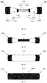
- the present invention also provides an improved method for manufacturing an electric cable joint 300, the method illustrated in figure 1 comprising the steps of:
- the first layer to be applied is the inner semiconducting layer 311.
- This layer may be applied by lapping a pre-extruded tape.
- the inner semiconducting layer 311 may be a thermoplastic material containing a cross-linking agent, that will allow for the crosslinking of the inner semiconducting layer 311 upon heating or other activation (e.g. moisture or radiation). The material is heated above the crystalline melting point and shaped into a cylinder around the conductor and crosslinked. The crosslinking will give the material thermal and mechanical stability which will make the layer 311 not deformable while applying other layers. Forming an even cylinder is desirable.
- the inner semiconducting layer 311 may, depending on the circumstances, also be formed by using a pre-moulded part, or by 3D printing.
- the intermediate insulating layer 312 can then be formed on top of the crosslinked inner semiconducting layer by several methods.
- a first method consists in using tape lapping.
- the intermediate insulating and outer semiconducting materials are extruded as a tape and applied helically on top of the crosslinked inner semiconducting layer 311, then heated above melting temperature, shaped and cooled.
- These two layers (312, 313) may be formed one after the other, or both tapes can be applied before being heated above melting temperature, shaped and cooled at the same time.
- a second method could include either (i) direct injection moulding of the insulating material onto the crosslinked inner semiconducting layer 311, or (ii) the use of at least one pre-moulded element, for example as two halves (shown in Figure 2 ), or in its entirety but with slits, so that it can be clamped onto the inner semiconducting layer 311.
- Heat and pressure can then be applied to melt the piece(s) in place and thus form the intermediate insulating layer 312.
- this second method significantly reduces the amount of material interfaces and the risk for contamination, though cleanliness will as usual be a key factor for success.
- the problem of material flow may be solved since the voids associated with lapping will be close to eliminated and it will be possible to apply equal pressure on the joint and the cable on its side all the way to outside the heated zone so that the material is held in place. This is not as easy when dealing with a lapped joint because the volume change is different in the joint compared to the surrounding cable due to the voids introduced between laps. This also has the potential to be a much less labour-intensive method. If so, there is also the possibility to reduce the cost in crosslinked PE jointing since the tape extrusion and lapping steps may be avoided.
- the final outer semiconducting layer 313 may be added by tape lapping, by using at least one pre-moulded element, by direct injection or any other method known in the art.
- the 3D printer's arm 31 advances 32 and rotates 33 around the inner semiconducting layer 311 while depositing insulating material to form the intermediate insulating layer 312.
- the outer semiconducting layer may also be 3-D printed on the intermediate insulating layer.
- the 3D printer's arm 41 advances 42 and rotates 43 around the intermediate insulating layer 312 while depositing the second semiconducting material to form the outer semiconducting layer 313.
- the methods for producing the intermediate and outer layers 312, 313 are independent from each other.
- Thermoplastic materials are defined as polymers that can be melted and recast almost indefinitely. They are molten when heated and harden upon cooling. The polymer network of a thermoplastic material forms and/or breaks up as the temperature is changed.
- Crosslinking is the general term for the process of forming covalent bonds or relatively short sequences of chemical bonds to join two polymer chains together.
- a crosslinked polymer is a polymer that has undergone the crosslinking process.
- Typical crosslinking processes known in the art can be used to obtain the desired crosslinking, for example cured by heat, pressure, radiation or similar.
- the inner semiconducting layer 311 may for instance be made of a polymer matrix selected from one or more polyolefins such as, for example but not limited to: polypropylenes of various stereoregularity (atactic PP, isotactic PP, syndiotactic PP etc), block copolymer polypropylenes, and PP copolymers, polyethylene (PE, HDPE, LDPE, LLDPE, MDPE) and its copolymers, thermoplastic olefins (TPOs), and a mixture of thereof.
- polyolefins such as, for example but not limited to: polypropylenes of various stereoregularity (atactic PP, isotactic PP, syndiotactic PP etc), block copolymer polypropylenes, and PP copolymers, polyethylene (PE, HDPE, LDPE, LLDPE, MDPE) and its copolymers, thermoplastic olefins (
- Additives to increase conductivity such as acetylene black, furnace black, carbon nanotubes, graphene and the likes or any combination thereof may be added to the polymer, to obtain the desired semiconductive properties.
- the inner semiconducting layer 311 may also comprise a dielectric fluid.
- the inner semiconducting layer 311 may also comprise other additives, such as antioxidants, stabilizers, etc.
- the inner semiconducting layer 311 may also comprise a crosslinking agent such as a peroxide (for example dicumyl peroxide, di-tert-butyl peroxide, cumene hydroperoxide, 1,3-bis(tert-butylperoxyisopropyl)benzene and similar).
- a peroxide for example dicumyl peroxide, di-tert-butyl peroxide, cumene hydroperoxide, 1,3-bis(tert-butylperoxyisopropyl)benzene and similar).
- the inner semiconducting layer 311 may also comprise a crosslinking boosting agent such as, for example, trimethylolpropane trimethacrylate (TMPTMA) and similar, or a polyolefin copolymer boasting insaturations such as vinyl groups, C-C ⁇ -bonds etc.
- TMPTMA trimethylolpropane trimethacrylate
- TMPTMA polyolefin copolymer boasting insaturations such as vinyl groups, C-C ⁇ -bonds etc.
- the intermediate insulating layer 312 may for instance be made of thermoplastic polyolefins (TPO), polypropylene, polypropylene and its copolymers with ethylene, HDPE, LLDPE, LDPE, MDPE, PE-based copolymers etc. or any combination thereof.
- TPO thermoplastic polyolefins
- polypropylene polypropylene and its copolymers with ethylene, HDPE, LLDPE, LDPE, MDPE, PE-based copolymers etc. or any combination thereof.
- an insulating material could comprise PP, TPO and LLDPE.
- the outer semiconducting layer 313 may for instance be made of thermoplastic polyolefins (TPO), polypropylene, polypropylene and its copolymers with ethylene, HDPE, LLDPE, LDPE, MDPE, PE-based copolymers etc. or any combination thereof.
- TPO thermoplastic polyolefins
- Conductive filler such as furnace black, acetylene black, etc. or any combination thereof may be added to the polymer, to obtain the desired semiconductive properties.
- both the insulating and the semiconducting materials may further comprise additives such as plasticizers, fillers (including nanomaterials), stabilizers, processing aids, etc.
Landscapes
- Processing Of Terminals (AREA)
Abstract
Description
- The present invention relates to high voltage electric cable connections. More particularly, the invention relates to a mixed crosslinked and thermoplastic insulation system for jointing of high voltage conductors and to a method for jointing of high voltage conductors.
-
EP0079118 describes a multilayer, heat shrinkable composite tube covering for a cable joint structure in which intimately joined layers define a semiconductive inner conductor shield, an insulation layer, and an outer insulation shield. The joint comprises an inner semi-conducting layer, an intermediate insulation layer and an outer semi-conducting layer. Each layer is made of a cured or crosslinked polymer. -
EP0379056 describes joints of electric cables and a tubular covering for joints which is destined to encircle the connection between the conductors of the cables and to tighten elastically on the ends of these latter which face each other. The joint comprises an inner semi-conducting layer, an intermediate insulation layer and an outer semi-conducting layer. Each layer is made of a crosslinked polymeric material. -
EP3365952 describes a joint for medium/high voltage electric cables having a thermoplastic insulation system. The insulation system comprises an inner semi-conducting layer, an intermediate insulation layer and an outer semi-conducting layer. Each layer is made of a thermoplastic polymeric material. -
WO2015197686 describes a joint for high voltage electric cables having an insulation system. The insulation system comprises an inner semi-conducting layer, an intermediate insulation layer and an outer semi-conducting layer. Each layer is made of a thermoplastic polymeric material. - Several solutions for insulation system for jointing of high voltage conductors are known, but all have various disadvantages that should be overcome.
- One such problem when integrating thermoplastic polymeric material in the insulation system of the joint is that the traditional lapping method may not be viable anymore since the lack of cross-linking will allow material deformation during the melting procedure. An alternative is to use a direct injection moulding procedure. However, this procedure requires highly specialized equipment and the jointing needs to be performed in two steps in order to account for density/volume change in the material.
- The goal of the present invention is to provide a new and advantageous insulation system for jointing of high voltage conductors. In particular, the present invention provides a mixed crosslinked and thermoplastic insulation system for jointing of high voltage conductors.
- The present invention is defined by the appended claims and in the following.
- In a first aspect, the present invention provides a joint for joining a first electric cable and a second electric cable, each cable comprising an electric conductor and an insulation system surrounding the electric conductor, the insulation system comprising an inner semiconducting layer, an insulating layer and an outer semiconducting layer, wherein the end sections of the two electrical conductors form an electrical conductor joint; the joint comprising:
- an inner layer made of a crosslinked first polymeric semiconducting material, for surrounding the electric conductor joint,
- an intermediate insulating layer made of a thermoplastic polymeric insulating material, covering an external surface of the inner semiconducting layer, and
- an outer layer made of a second polymeric semiconducting material, covering an external surface of the insulating layer.
- Thermoplastic materials are defined as polymers that can be melted and recast almost indefinitely. They are molten when heated and harden upon cooling. The polymer network of a thermoplastic material forms and/or breaks up as the temperature is changed.
Crosslinking is the general term for the process of forming covalent bonds or relatively short sequences of chemical bonds to join two polymer chains together. - A crosslinked polymer is a polymer that has undergone the crosslinking process.
- Here the person skilled in the art will understand that when a layer is described to be made of a crosslinked polymer, it means that the crosslinking can happen before or after the formation of the layer.
- Typical crosslinking processes known in the art can be used to obtain the desired crosslinking, for example cured by heat, pressure, radiation or similar.
- In an embodiment of the joint, the inner semiconducting layer is in direct contact with the electrical conductor.
- In an embodiment of the joint, the second polymeric semiconducting material may be a thermoplastic semiconducting material.
- In an alternative embodiment of the joint, the second polymeric semiconducting material may be a crosslinked semiconducting material.
In an embodiment of the joint, the intermediate insulating layer is in direct contact with the inner semiconducting layer. - In an embodiment, the thermoplastic polymeric insulating material comprises a polymer matrix selected from one or more polyolefins such as, for example but not limited to: polypropylenes of various stereoregularity (atactic PP, isotactic PP, syndiotactic PP etc), block copolymer polypropylenes, and PP copolymers, polyethylene (PE, HDPE, LDPE, LLDPE, MDPE) and its copolymers, thermoplastic olefins (TPOs), and a mixture of thereof.
- In another embodiment, the thermoplastic polymeric insulating material comprises a dielectric fluid.
- In another embodiment, the thermoplastic polymeric insulating material comprises additives such as antioxidants, stabilizers, etc.
- In another embodiment, the thermoplastic polymeric insulating material comprises a polymer matrix selected from one or more polyolefins such as polypropylene and its copolymers, thermoplastic olefins (TPOs), or mixture of thereof; optionally a dielectric fluid; and optionally additives such as antioxidants, stabilizers, etc.
- In an embodiment, the crosslinked first polymeric semiconducting material comprises a polymer matrix selected from one or more polyolefins such as, for example but not limited to: polypropylenes of various stereoregularity (atactic PP, isotactic PP, syndiotactic PP etc), block copolymer polypropylenes, and PP copolymers, polyethylene (PE, HDPE, LDPE, LLDPE, MDPE) and its copolymers, thermoplastic olefins (TPOs), and a mixture of thereof.
- In another embodiment, the crosslinked first polymeric semiconducting material comprises additives to increase conductivity such as acetylene black, furnace black, carbon nanotubes, graphene and the likes, and combinations thereof.
- In another embodiment, the crosslinked first polymeric semiconducting material comprises a dielectric fluid.
- In another embodiment, the crosslinked first polymeric semiconducting material comprises additives such as antioxidants, stabilizers, etc.
- In another embodiment, the crosslinked first polymeric semiconducting material comprises a crosslinking agent such as a peroxide (for example dicumyl peroxide, di-tert-butyl peroxide, cumene hydroperoxide, 1,3-bis(tert-butylperoxyisopropyl)benzene and similar).
- In another embodiment, the crosslinked first polymeric semiconducting material comprises a crosslinking boosting agent such as, for example, trimethylolpropane trimethacrylate (TMPTMA) and similar, or a polyolefin copolymer boasting insaturations such as vinyl groups, C-C π-bonds etc.
In an embodiment, the crosslinked first polymeric semiconducting material comprises a polymer matrix selected from a single material or a mixture of materials such as PP and its copolymers, PE and its copolymers or thermoplastic olefins (TPOs); an additive to increase conductivity such as acetylene black, furnace black, carbon nanotubes, graphene and the likes; optionally a dielectric fluid; optionally additives such as antioxidants, stabilizers, etc; optionally a crosslinking agent such as a peroxide and optionally a crosslinking boosting agent. - In an embodiment, the second polymeric semiconducting material comprises a polymer matrix selected from one or more polyolefins such as, for example but not limited to: polypropylenes of various stereoregularity (atactic PP, isotactic PP, syndiotactic PP etc), block copolymer polypropylenes, and PP copolymers, polyethylene (PE, HDPE, LDPE, LLDPE, MDPE) and its copolymers, thermoplastic olefins (TPOs), and a mixture of thereof.
- In an embodiment, the second polymeric semiconducting material comprises additives to increase conductivity such as acetylene black, furnace black, carbon nanotubes, graphene and the likes and combinations thereof.
- In an embodiment, the second polymeric semiconducting material comprises a dielectric fluid.
- In an embodiment, the second polymeric semiconducting material comprises additives such as antioxidants, stabilizers, etc.
- In an embodiment, the second polymeric semiconducting material comprises a polymer matrix selected from a single material or a mixture of materials such as PP and its copolymers, PE and its copolymers or thermoplastic olefins (TPOs); an additive to increase conductivity such as acetylene black, furnace black, carbon nanotubes, graphene and the likes; optionally a dielectric fluid; and optionally additives such as antioxidants, stabilizers, etc.
- In an embodiment of the joint, the first electric cable has a thermoplastic insulation system, i.e. all layers of the insulation system surrounding the electric conductor are made of a thermoplastic polymer.
- In another embodiment of the joint, the first electric cable has a crosslinked insulation system, i.e. all layers of the insulation system surrounding the electric conductor are made of a crosslinked polymer.
- In another embodiment of the joint, the first and the second electric cables have a thermoplastic insulation system.
- In another embodiment of the joint, the first and the second electric cables have a crosslinked insulation system.
- In another embodiment of the joint, one of the first and the second electric cables has a thermoplastic insulation system while the other has a crosslinked insulation system.
- In another embodiment of the joint, at least one of the layers of the insulation system surrounding the electric conductor of the first and/or the second electrical cable is a thermoplastic insulation system.
- In another embodiment of the joint, the inner semiconducting layer, the insulating layer and the outer semiconducting layer are each thermoplastic material.
- In another embodiment of the joint, each cable, the inner semiconducting layer, the insulating layer and the outer semiconducting layer are each made of thermoplastic material.
- In a second aspect, the present invention provides a method for manufacturing an electric cable joint, the method comprising the steps of:
- a) providing a first and a second electric cables, each cable comprising an electric conductor and an insulation system surrounding the electric conductor, the insulation system comprising an inner semiconducting layer, an insulating layer and an outer semiconducting layer;
- b) joining the respective terminal portions of the electric conductors of the first electric cable and of the second electric cable to form an electric conductor joint;
- c) surrounding the electric conductor joint with a joint inner layer made of a crosslinked first semiconducting material;
- d) surrounding the joint inner layer with a joint insulating layer made of a thermoplastic insulating material; and
- e) surrounding the joint insulating layer with a joint outer layer made of a second semiconducting material.
- In other words, the terminal portion of the first electric conductor is placed axially adjacent to the terminal portion of the second electric conductor when the electric conductors are joined.
- Although steps c), d), and e) are described as consecutive steps in the method, the person skilled in the art will understand that in some cases it will be advantageous to perform these steps at the same time.
- In an embodiment of the method, the first polymeric material, the second polymeric material etc. may be as defined for the joint according to the first aspect of the invention.
- In another embodiment of the method, the crosslinked first semiconducting material may be applied by tape lapping, and optionally degassed in step c) to form the joint inner layer.
- In another embodiment, the thermoplastic insulating material may be applied by tape lapping, injection moulding, 3D-printing or as a pre-moulded part in step d) to form the joint insulating layer.
- In another embodiment, the second semiconducting material may be applied by tape lapping, injection moulding, 3D-printing or as a pre-moulded element in step e) to form the joint insulating layer.
- In an embodiment of the method, the thermoplastic insulating material and the second semiconducting material may be provided in the form of at least a pre-moulded element. In other words, such that steps d) and e) may be performed at the same time.
- The at least one pre-moulded element is adapted for surrounding the electric conductor joint and constitutes a cylindrical layer around the previous layer. The person skilled in the art will understand that a cylindrical layer refers to a hollow cylindrical layer or a tube-shaped cylindrical layer.
- In a third aspect, the present invention provides a cable comprising a joint according to the first aspect of the invention.
- In an embodiment of the cable, the cable comprising two cable sections and a joint, each cable section comprising an electric conductor and an insulation system surrounding the electric conductor, the insulation system comprising an inner semiconducting layer, an insulating layer and an outer semiconducting layer, wherein the end sections of the two electrical conductors form an electrical conductor joint; the joint comprising:
- an inner layer made of a crosslinked first polymeric semiconducting material, for surrounding the electric conductor joint,
- an intermediate insulating layer made of a thermoplastic polymeric insulating material, covering an external surface of the inner semiconducting layer, and
- an outer layer made of a second polymeric semiconducting material, covering an external surface of the insulating layer.
- In an embodiment of the cable, at least one of the layers of the insulation system surrounding the electric conductor of at least one of the cable sections is made of a thermoplastic material.
- In an embodiment of the cable, for each cable section, the inner semiconducting layer, the insulating layer and the outer semiconducting layer are each made of thermoplastic material.
- The present invention is described in detail by reference to the following drawings:
-
Fig. 1a-1d is a cross-sectional view of the assembly of insulation elements around a conductor. -
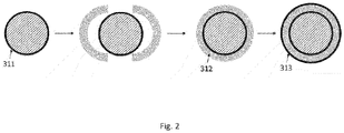
Fig. 2 is a side view of an embodiment of the jointing procedure when the intermediate layer is provided in the form of at least a pre-moulded element. -
Fig. 3 is a side view of an embodiment of the jointing procedure for depositing the intermediate layer by 3D printing. -
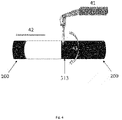
Fig. 4 is a side view of an embodiment of the jointing procedure for depositing the outer layer by 3D printing. - Jointing cables with a thermoplastic insulation system is challenging. The specific properties of thermoplastic polymers make it difficult if not impossible to adapt procedures known in the art, for example traditionally used with crosslinked polymer, where once set each layer will not be affected by the heating of the subsequent layer.
- Jointing cables with different types of insulation is likewise challenging. A joint is commonly made up of an inner semiconducting, insulation layer and outer semiconducting layer.
- A challenge in producing a fully thermoplastic insulation system is that after an additional thermoplastic layer is applied to build a joint, the additional thermoplastic layer needs to be heated to form a cylinder and insure the best contact with the previous layer. However, this additional thermoplastic layer (and potentially the previous layer underneath if made of thermoplastic material) may lose its shape during this step. This will in turn cause deformation and uniformity/homogeneity problems at the joint. These are critical parameters to insure a good insulation in the joint.
- This is most critical during the preparation of the intermediate insulating layer that is traditionally much thicker than the inner and outer semiconducting layers. Due to the thickness, the intermediate insulating layer requires extensive heating and there is a risk of deforming the inner semiconducting layer. By using a crosslinked material for the inner semiconducting layer, there is virtually no risk of deformation during the preparation of the intermediate insulating layer.
- Oppositely, it is not a problem for the outer layer to be made of a thermoplastic polymer material since it is traditionally much thinner than the intermediate layer and does not require extensive heating that would deform the intermediate layer.
- The present invention provides an improved joint 300 comprising
- an
inner layer 311 made of a crosslinked first polymeric semiconducting material, for surrounding the electric conductor joint 310, - an insulating
layer 312 made of a thermoplastic polymeric insulating material, covering an external surface of the innersemiconducting layer 311, and - an
outer layer 313 made of a second polymeric semiconducting material, covering an external surface of the intermediate insulatinglayer 312. - The present invention also provides an improved method for manufacturing an
electric cable joint 300, the method illustrated infigure 1 comprising the steps of: - providing a first and a second
electric cables 100; 200, each cable comprising anelectric conductor 110; 210 and aninsulation system 120; 220, surrounding theelectric conductor 110; 210, theinsulation system 120; 220 comprising an innersemiconducting layer 121; 221, a insulatinglayer 122; 222 and an outersemiconducting layer 123; 223; - joining the respective terminal portions of the
electric conductors 110; 210 of the first electric cable and of a second electric cable placed axially adjacent to the first electric cable, to form an electric conductor joint 310; (Figure 1a ) - surrounding the electric conductor joint 310 with a joint
inner layer 311 of a crosslinked first semiconducting material; (Figure 1b ) - surrounding the joint
inner layer 311 of crosslinked first semiconducting material with a joint insulatinglayer 312 of a thermoplastic insulating material (Figure 1c ); and - surrounding the joint insulating
layer 312 of thermoplastic insulating material with a jointouter layer 313 of a second semiconducting material (Figure 1d ). - After jointing the conductor and preparing the cable joint 310 (
Figure 1a ), the first layer to be applied is the innersemiconducting layer 311. This layer may be applied by lapping a pre-extruded tape. The innersemiconducting layer 311 may be a thermoplastic material containing a cross-linking agent, that will allow for the crosslinking of the innersemiconducting layer 311 upon heating or other activation (e.g. moisture or radiation). The material is heated above the crystalline melting point and shaped into a cylinder around the conductor and crosslinked. The crosslinking will give the material thermal and mechanical stability which will make thelayer 311 not deformable while applying other layers. Forming an even cylinder is desirable. Alternatively, the innersemiconducting layer 311 may, depending on the circumstances, also be formed by using a pre-moulded part, or by 3D printing. - The intermediate
insulating layer 312 can then be formed on top of the crosslinked inner semiconducting layer by several methods. - A first method consists in using tape lapping. In this method the intermediate insulating and outer semiconducting materials are extruded as a tape and applied helically on top of the crosslinked inner
semiconducting layer 311, then heated above melting temperature, shaped and cooled. These two layers (312, 313) may be formed one after the other, or both tapes can be applied before being heated above melting temperature, shaped and cooled at the same time. - A second method could include either (i) direct injection moulding of the insulating material onto the crosslinked inner
semiconducting layer 311, or (ii) the use of at least one pre-moulded element, for example as two halves (shown inFigure 2 ), or in its entirety but with slits, so that it can be clamped onto the innersemiconducting layer 311. - Heat and pressure can then be applied to melt the piece(s) in place and thus form the intermediate insulating
layer 312. - Compared to the traditional lapping procedure, this second method (direct injection or using pre-moulded elements) significantly reduces the amount of material interfaces and the risk for contamination, though cleanliness will as usual be a key factor for success.
- By using direct injection or already having the pieces in their final form the problem of material flow may be solved since the voids associated with lapping will be close to eliminated and it will be possible to apply equal pressure on the joint and the cable on its side all the way to outside the heated zone so that the material is held in place. This is not as easy when dealing with a lapped joint because the volume change is different in the joint compared to the surrounding cable due to the voids introduced between laps. This also has the potential to be a much less labour-intensive method. If so, there is also the possibility to reduce the cost in crosslinked PE jointing since the tape extrusion and lapping steps may be avoided.
- The final outer
semiconducting layer 313 may be added by tape lapping, by using at least one pre-moulded element, by direct injection or any other method known in the art. - By 3-D printing the insulating material directly onto the crosslinked inner semiconducting layer, as illustrated in
figure 3 , the problem of material flow compared to applying tapes may also be solved. Moreover, it is possible to have the 3-D printing process carried out in a glove-box, highly improving the cleanliness of the process and reducing risk of electrical breakdown due to pollutants. This also has the potential to be a much less labour-intensive method. - In a word, as shown in
figure 3 , the 3D printer'sarm 31 advances 32 and rotates 33 around the innersemiconducting layer 311 while depositing insulating material to form the intermediate insulatinglayer 312. - If so, there is also the possibility to reduce the cost in crosslinked PE jointing since the tape extrusion and lapping steps may be avoided.
- As shown in
figure 4 , the outer semiconducting layer may also be 3-D printed on the intermediate insulating layer. In a word, the 3D printer'sarm 41 advances 42 and rotates 43 around the intermediate insulatinglayer 312 while depositing the second semiconducting material to form the outersemiconducting layer 313. - The methods for producing the intermediate and
outer layers - Thermoplastic materials are defined as polymers that can be melted and recast almost indefinitely. They are molten when heated and harden upon cooling. The polymer network of a thermoplastic material forms and/or breaks up as the temperature is changed.
- Crosslinking is the general term for the process of forming covalent bonds or relatively short sequences of chemical bonds to join two polymer chains together.
- A crosslinked polymer is a polymer that has undergone the crosslinking process. Typical crosslinking processes known in the art can be used to obtain the desired crosslinking, for example cured by heat, pressure, radiation or similar.
- The inner
semiconducting layer 311 may for instance be made of a polymer matrix selected from one or more polyolefins such as, for example but not limited to: polypropylenes of various stereoregularity (atactic PP, isotactic PP, syndiotactic PP etc), block copolymer polypropylenes, and PP copolymers, polyethylene (PE, HDPE, LDPE, LLDPE, MDPE) and its copolymers, thermoplastic olefins (TPOs), and a mixture of thereof. - Additives to increase conductivity such as acetylene black, furnace black, carbon nanotubes, graphene and the likes or any combination thereof may be added to the polymer, to obtain the desired semiconductive properties.
- The inner
semiconducting layer 311 may also comprise a dielectric fluid. - The inner
semiconducting layer 311 may also comprise other additives, such as antioxidants, stabilizers, etc. - The inner
semiconducting layer 311 may also comprise a crosslinking agent such as a peroxide (for example dicumyl peroxide, di-tert-butyl peroxide, cumene hydroperoxide, 1,3-bis(tert-butylperoxyisopropyl)benzene and similar). - The inner
semiconducting layer 311 may also comprise a crosslinking boosting agent such as, for example, trimethylolpropane trimethacrylate (TMPTMA) and similar, or a polyolefin copolymer boasting insaturations such as vinyl groups, C-C π-bonds etc. - The intermediate
insulating layer 312 may for instance be made of thermoplastic polyolefins (TPO), polypropylene, polypropylene and its copolymers with ethylene, HDPE, LLDPE, LDPE, MDPE, PE-based copolymers etc. or any combination thereof.
For example, an insulating material could comprise PP, TPO and LLDPE. - The outer
semiconducting layer 313 may for instance be made of thermoplastic polyolefins (TPO), polypropylene, polypropylene and its copolymers with ethylene, HDPE, LLDPE, LDPE, MDPE, PE-based copolymers etc. or any combination thereof. Conductive filler such as furnace black, acetylene black, etc. or any combination thereof may be added to the polymer, to obtain the desired semiconductive properties. - To achieve desired material properties, both the insulating and the semiconducting materials may further comprise additives such as plasticizers, fillers (including nanomaterials), stabilizers, processing aids, etc.
Claims (15)
- A joint (300) for joining a first electric cable (100) and a second electric cable (200), each cable (100; 200) comprising an electric conductor (110; 210) and an insulation system (120; 220) surrounding the electric conductor (110; 210), the insulation system (120; 220) comprising an inner semiconducting layer (121; 221), an insulating layer (122; 222) and an outer semiconducting layer (123; 223), wherein the end sections of the two electrical conductors (110; 210) form an electrical conductor joint (310);
the joint (300) comprising:- an inner layer (311) made of a crosslinked first polymeric semiconducting material, for surrounding the electric conductor joint (310),- an intermediate insulating layer (312) made of a thermoplastic polymeric insulating material, covering an external surface of the inner semiconducting layer (311), and- an outer layer (313) made of a second polymeric semiconducting material, covering an external surface of the insulating layer (312). - A joint according to claim 1, wherein the second polymeric semiconducting material is a thermoplastic semiconducting material.
- A joint according to claim 1, wherein the second polymeric semiconducting material is a crosslinked semiconducting material.
- A joint according to any one of the previous claims, wherein at least one of the layers (121; 221; 122; 222; 123; 223) of the insulation system (120; 220) surrounding the electric conductor (110; 210) of the first and/or the second electrical cable is made of thermoplastic material.
- A joint according to claim 4, wherein the inner semiconducting layer (121; 221), the insulating layer (122; 222) and the outer semiconducting layer (123; 223) are each made of thermoplastic material.
- A joint according to claim 4 or 5, wherein, for each cable (100; 200) the inner semiconducting layer (121; 221), the insulating layer (122; 222) and the outer semiconducting layer (123; 223) are each made of thermoplastic material.
- A method for manufacturing an electric cable joint (300), the method comprising the steps of:a) providing a first and a second electric cables (100; 200), each cable comprising an electric conductor (110; 210) and an insulation system (120; 220) surrounding the electric conductor (110; 210), the insulation system (120; 220) comprising an inner semiconducting layer (121; 221), an insulating layer (122; 222) and an outer semiconducting layer (123; 223);b) joining the respective terminal portions of the electric conductors (110; 210) of the first electric cable and of the second electric cable to form an electric conductor joint (310);c) surrounding the electric conductor joint (310) with a joint inner layer (311) made of a crosslinked first polymeric semiconducting material;d) surrounding the joint inner layer (311) with a joint insulating layer (312) made of a thermoplastic insulating material; ande) surrounding the joint insulating layer (312) with a joint outer layer (313) made of a second polymeric semiconducting material.
- A method according to claim 7, wherein the second polymeric semiconducting material is a crosslinked semiconducting material.
- A method according to claim 7, wherein the second polymeric semiconducting material is a thermoplastic semiconducting material.
- A method according to any one of claims 7-9, wherein the crosslinked first polymeric semiconducting material is applied by tape lapping and optionally degassed in step c) to form the joint inner layer (311).
- A method according to any one of claims 7-10, wherein the thermoplastic insulating material is applied by tape lapping, injection moulding, 3D-printing or as a pre-moulded part in step d) to form the joint insulating layer (312).
- A method according to any one of claims 7-11, wherein the second polymeric semiconducting material is applied by tape lapping, injection moulding, 3D-printing or as a pre-moulded part in step e) to form the joint insulating layer (313).
- A cable comprising two cable sections (100; 200) and a joint (300), each cable section (100; 200) comprising an electric conductor (110; 210) and an insulation system (120; 220) surrounding the electric conductor (110; 210), the insulation system (120; 220) comprising an inner semiconducting layer (121; 221), an insulating layer (122; 222) and an outer semiconducting layer (123; 223),
wherein the end sections of the two electrical conductors (110; 210) form an electrical conductor joint (310);
the joint (300) comprising:- an inner layer (311) made of a crosslinked first polymeric semiconducting material, for surrounding the electric conductor joint (310),- an intermediate insulating layer (312) made of a thermoplastic polymeric insulating material, covering an external surface of the inner semiconducting layer (311), and- an outer layer (313) made of a second polymeric semiconducting material, covering an external surface of the insulating layer (312). - A cable according to claim 13, wherein at least one of the layers (121; 221; 122; 222; 123; 223) of the insulation system (120; 220) surrounding the electric conductor (110; 210) of at least one of the cable sections is made of thermoplastic material.
- A cable according to claim 14, wherein, for each cable section (100; 200), the inner semiconducting layer (121; 221), the insulating layer (122; 222) and the outer semiconducting layer (123; 223) are each made of thermoplastic material.
Priority Applications (2)
| Application Number | Priority Date | Filing Date | Title |
|---|---|---|---|
| EP21305568.4A EP4084247A1 (en) | 2021-04-30 | 2021-04-30 | Joint for electrical cables and method for jointing |
| US17/731,171 US12230944B2 (en) | 2021-04-30 | 2022-04-27 | Joint for electrical cables and method for jointing |
Applications Claiming Priority (1)
| Application Number | Priority Date | Filing Date | Title |
|---|---|---|---|
| EP21305568.4A EP4084247A1 (en) | 2021-04-30 | 2021-04-30 | Joint for electrical cables and method for jointing |
Publications (1)
| Publication Number | Publication Date |
|---|---|
| EP4084247A1 true EP4084247A1 (en) | 2022-11-02 |
Family
ID=75904848
Family Applications (1)
| Application Number | Title | Priority Date | Filing Date |
|---|---|---|---|
| EP21305568.4A Pending EP4084247A1 (en) | 2021-04-30 | 2021-04-30 | Joint for electrical cables and method for jointing |
Country Status (2)
| Country | Link |
|---|---|
| US (1) | US12230944B2 (en) |
| EP (1) | EP4084247A1 (en) |
Cited By (1)
| Publication number | Priority date | Publication date | Assignee | Title |
|---|---|---|---|---|
| EP4521574A1 (en) * | 2023-09-07 | 2025-03-12 | NKT HV Cables AB | Dc power cable system |
Families Citing this family (1)
| Publication number | Priority date | Publication date | Assignee | Title |
|---|---|---|---|---|
| EP4049834A1 (en) * | 2021-02-25 | 2022-08-31 | Nexans | Thermoplastic insulation system |
Citations (7)
| Publication number | Priority date | Publication date | Assignee | Title |
|---|---|---|---|---|
| GB2108329A (en) * | 1981-10-29 | 1983-05-11 | Pirelli General Cable Works | Joining electric cables |
| EP0079118A1 (en) | 1981-11-09 | 1983-05-18 | Cable Technology Laboratories, Inc. | Electrical cable joint structure and method of manufacture |
| EP0379056A2 (en) | 1989-01-16 | 1990-07-25 | PIRELLI CAVI S.p.A. | Element of a device for realizing a joint of electric cables, joint for electric cables obtained thereby, and covering of the connection between the conductors of electric cables for said joint |
| JP2000228813A (en) * | 1999-02-08 | 2000-08-15 | Fujikura Ltd | How to connect the power cable |
| WO2015197686A1 (en) | 2014-06-25 | 2015-12-30 | Abb Technology Ltd | An insulation system for hv cable joint, a method for forming a joint and a cable joint |
| US20170309366A1 (en) * | 2014-09-26 | 2017-10-26 | Nexans | Electrical Device Comprising a Cross-linked Layer |
| EP3365952A1 (en) | 2015-10-23 | 2018-08-29 | Prysmian S.p.A. | Joint for electric cables with thermoplastic insulation and method for manufacturing the same |
Family Cites Families (6)
| Publication number | Priority date | Publication date | Assignee | Title |
|---|---|---|---|---|
| WO2012044523A1 (en) * | 2010-09-30 | 2012-04-05 | Dow Global Technologies Llc | Recyclable thermoplastic insulation with improved breakdown strength |
| US9178289B2 (en) * | 2013-05-14 | 2015-11-03 | Tyco Electronics Corporation | Joint bodies and methods for covering electrical cables and connections |
| FR3026899B1 (en) * | 2014-10-03 | 2016-10-28 | Nexans | FIRE RESISTANT CABLES CONNECTION |
| CN108780676B (en) * | 2015-11-23 | 2020-10-27 | Nkt Hv 电缆有限责任公司 | Flexible vulcanized joint between two power cables and method of producing the joint |
| EP3336993B1 (en) * | 2016-12-19 | 2021-11-10 | Nexans | Cable reinforcement sleeve for subsea cable joint |
| CN211980229U (en) * | 2020-04-22 | 2020-11-20 | 浙江万马股份有限公司 | A kind of high insulation power cable |
-
2021
- 2021-04-30 EP EP21305568.4A patent/EP4084247A1/en active Pending
-
2022
- 2022-04-27 US US17/731,171 patent/US12230944B2/en active Active
Patent Citations (7)
| Publication number | Priority date | Publication date | Assignee | Title |
|---|---|---|---|---|
| GB2108329A (en) * | 1981-10-29 | 1983-05-11 | Pirelli General Cable Works | Joining electric cables |
| EP0079118A1 (en) | 1981-11-09 | 1983-05-18 | Cable Technology Laboratories, Inc. | Electrical cable joint structure and method of manufacture |
| EP0379056A2 (en) | 1989-01-16 | 1990-07-25 | PIRELLI CAVI S.p.A. | Element of a device for realizing a joint of electric cables, joint for electric cables obtained thereby, and covering of the connection between the conductors of electric cables for said joint |
| JP2000228813A (en) * | 1999-02-08 | 2000-08-15 | Fujikura Ltd | How to connect the power cable |
| WO2015197686A1 (en) | 2014-06-25 | 2015-12-30 | Abb Technology Ltd | An insulation system for hv cable joint, a method for forming a joint and a cable joint |
| US20170309366A1 (en) * | 2014-09-26 | 2017-10-26 | Nexans | Electrical Device Comprising a Cross-linked Layer |
| EP3365952A1 (en) | 2015-10-23 | 2018-08-29 | Prysmian S.p.A. | Joint for electric cables with thermoplastic insulation and method for manufacturing the same |
Cited By (1)
| Publication number | Priority date | Publication date | Assignee | Title |
|---|---|---|---|---|
| EP4521574A1 (en) * | 2023-09-07 | 2025-03-12 | NKT HV Cables AB | Dc power cable system |
Also Published As
| Publication number | Publication date |
|---|---|
| US12230944B2 (en) | 2025-02-18 |
| US20220376483A1 (en) | 2022-11-24 |
Similar Documents
| Publication | Publication Date | Title |
|---|---|---|
| FI69943B (en) | FOERFARANDE FOER BILDANDE AV EN FOERBINDNING FOER EN POLYOLEFINISOLERAD ELEKTRISK LEDNING ELLER KABEL OCH VAERMEKRYMPANDE SLANG FOER GENOMFOERANDE AV FOERFARANDET | |
| US12230944B2 (en) | Joint for electrical cables and method for jointing | |
| CA1200586A (en) | Electrical cable joint structure and method of manufacture | |
| EP3539188B1 (en) | Process for jointing cables | |
| US4289721A (en) | Method of connecting cables | |
| WO2015197686A1 (en) | An insulation system for hv cable joint, a method for forming a joint and a cable joint | |
| US12272936B2 (en) | Method of jointing a power cable | |
| US20240055850A1 (en) | Thermoplastic insulation system | |
| US20200035383A1 (en) | Assembly and method for sealing a bundle of wires | |
| FI66999B (en) | SAETT VIDAR SCARVES AV EN CABLE WITH ISOLERING AV TVAERBUNDEN POYETEN ELLER ANNAN TVAERBUNDEN POLYMER | |
| GB2074931A (en) | Recoverable articles | |
| JPS6023476B2 (en) | Method for forming connections of insulated cables | |
| JPS5810385A (en) | Method for forming connections of insulated cables | |
| DE3511299C2 (en) | ||
| US20250079811A1 (en) | Flexible joint for power cable | |
| JP2000164046A (en) | Power cable and its laying method | |
| JP3012514B2 (en) | CV cable insulation connection method | |
| JP3012515B2 (en) | CV cable insulation connection method | |
| JPH02142312A (en) | Method for forming insulation at power cable connections | |
| JPH08236242A (en) | Method for forming extruded mold type connection part of crosslinked polyolefin insulated cable | |
| JPS6057657B2 (en) | Method of forming insulated cable connections | |
| JPS6364276A (en) | Molding method for plastic insulated cable connections | |
| JPH09284943A (en) | Method for extrusion mold joint of bridgeable polyethylene cable | |
| JPS6231315A (en) | Formation for connection of insulated cable | |
| JPS6114639B2 (en) |
Legal Events
| Date | Code | Title | Description |
|---|---|---|---|
| PUAI | Public reference made under article 153(3) epc to a published international application that has entered the european phase |
Free format text: ORIGINAL CODE: 0009012 |
|
| STAA | Information on the status of an ep patent application or granted ep patent |
Free format text: STATUS: THE APPLICATION HAS BEEN PUBLISHED |
|
| AK | Designated contracting states |
Kind code of ref document: A1 Designated state(s): AL AT BE BG CH CY CZ DE DK EE ES FI FR GB GR HR HU IE IS IT LI LT LU LV MC MK MT NL NO PL PT RO RS SE SI SK SM TR |
|
| STAA | Information on the status of an ep patent application or granted ep patent |
Free format text: STATUS: REQUEST FOR EXAMINATION WAS MADE |
|
| 17P | Request for examination filed |
Effective date: 20230502 |
|
| RBV | Designated contracting states (corrected) |
Designated state(s): AL AT BE BG CH CY CZ DE DK EE ES FI FR GB GR HR HU IE IS IT LI LT LU LV MC MK MT NL NO PL PT RO RS SE SI SK SM TR |
|
| STAA | Information on the status of an ep patent application or granted ep patent |
Free format text: STATUS: EXAMINATION IS IN PROGRESS |
|
| 17Q | First examination report despatched |
Effective date: 20250313 |