EP4084059A1 - Semiconductor device package having thermal dissipation feature and method therefor - Google Patents
Semiconductor device package having thermal dissipation feature and method therefor Download PDFInfo
- Publication number
- EP4084059A1 EP4084059A1 EP22168665.2A EP22168665A EP4084059A1 EP 4084059 A1 EP4084059 A1 EP 4084059A1 EP 22168665 A EP22168665 A EP 22168665A EP 4084059 A1 EP4084059 A1 EP 4084059A1
- Authority
- EP
- European Patent Office
- Prior art keywords
- thermal conductive
- conductive structure
- package substrate
- package
- semiconductor device
- Prior art date
- Legal status (The legal status is an assumption and is not a legal conclusion. Google has not performed a legal analysis and makes no representation as to the accuracy of the status listed.)
- Pending
Links
Images






Classifications
-
- H—ELECTRICITY
- H10—SEMICONDUCTOR DEVICES; ELECTRIC SOLID-STATE DEVICES NOT OTHERWISE PROVIDED FOR
- H10W—GENERIC PACKAGES, INTERCONNECTIONS, CONNECTORS OR OTHER CONSTRUCTIONAL DETAILS OF DEVICES COVERED BY CLASS H10
- H10W40/00—Arrangements for thermal protection or thermal control
- H10W40/20—Arrangements for cooling
- H10W40/22—Arrangements for cooling characterised by their shape, e.g. having conical or cylindrical projections
- H10W40/226—Arrangements for cooling characterised by their shape, e.g. having conical or cylindrical projections characterised by projecting parts, e.g. fins to increase surface area
- H10W40/228—Arrangements for cooling characterised by their shape, e.g. having conical or cylindrical projections characterised by projecting parts, e.g. fins to increase surface area the projecting parts being wire-shaped or pin-shaped
-
- H—ELECTRICITY
- H10—SEMICONDUCTOR DEVICES; ELECTRIC SOLID-STATE DEVICES NOT OTHERWISE PROVIDED FOR
- H10W—GENERIC PACKAGES, INTERCONNECTIONS, CONNECTORS OR OTHER CONSTRUCTIONAL DETAILS OF DEVICES COVERED BY CLASS H10
- H10W40/00—Arrangements for thermal protection or thermal control
- H10W40/20—Arrangements for cooling
- H10W40/22—Arrangements for cooling characterised by their shape, e.g. having conical or cylindrical projections
-
- H—ELECTRICITY
- H10—SEMICONDUCTOR DEVICES; ELECTRIC SOLID-STATE DEVICES NOT OTHERWISE PROVIDED FOR
- H10W—GENERIC PACKAGES, INTERCONNECTIONS, CONNECTORS OR OTHER CONSTRUCTIONAL DETAILS OF DEVICES COVERED BY CLASS H10
- H10W44/00—Electrical arrangements for controlling or matching impedance
- H10W44/20—Electrical arrangements for controlling or matching impedance at high-frequency [HF] or radio frequency [RF]
-
- H—ELECTRICITY
- H10—SEMICONDUCTOR DEVICES; ELECTRIC SOLID-STATE DEVICES NOT OTHERWISE PROVIDED FOR
- H10W—GENERIC PACKAGES, INTERCONNECTIONS, CONNECTORS OR OTHER CONSTRUCTIONAL DETAILS OF DEVICES COVERED BY CLASS H10
- H10W70/00—Package substrates; Interposers; Redistribution layers [RDL]
- H10W70/01—Manufacture or treatment
- H10W70/02—Manufacture or treatment of conductive package substrates serving as an interconnection, e.g. of metal plates
-
- H—ELECTRICITY
- H05—ELECTRIC TECHNIQUES NOT OTHERWISE PROVIDED FOR
- H05K—PRINTED CIRCUITS; CASINGS OR CONSTRUCTIONAL DETAILS OF ELECTRIC APPARATUS; MANUFACTURE OF ASSEMBLAGES OF ELECTRICAL COMPONENTS
- H05K3/00—Apparatus or processes for manufacturing printed circuits
- H05K3/30—Assembling printed circuits with electric components, e.g. with resistors
- H05K3/32—Assembling printed circuits with electric components, e.g. with resistors electrically connecting electric components or wires to printed circuits
- H05K3/34—Assembling printed circuits with electric components, e.g. with resistors electrically connecting electric components or wires to printed circuits by soldering
- H05K3/341—Surface mounted components
- H05K3/3431—Leadless components
- H05K3/3436—Leadless components having an array of bottom contacts, e.g. pad grid array or ball grid array components
-
- H—ELECTRICITY
- H10—SEMICONDUCTOR DEVICES; ELECTRIC SOLID-STATE DEVICES NOT OTHERWISE PROVIDED FOR
- H10W—GENERIC PACKAGES, INTERCONNECTIONS, CONNECTORS OR OTHER CONSTRUCTIONAL DETAILS OF DEVICES COVERED BY CLASS H10
- H10W40/00—Arrangements for thermal protection or thermal control
- H10W40/20—Arrangements for cooling
- H10W40/22—Arrangements for cooling characterised by their shape, e.g. having conical or cylindrical projections
- H10W40/226—Arrangements for cooling characterised by their shape, e.g. having conical or cylindrical projections characterised by projecting parts, e.g. fins to increase surface area
-
- H—ELECTRICITY
- H10—SEMICONDUCTOR DEVICES; ELECTRIC SOLID-STATE DEVICES NOT OTHERWISE PROVIDED FOR
- H10W—GENERIC PACKAGES, INTERCONNECTIONS, CONNECTORS OR OTHER CONSTRUCTIONAL DETAILS OF DEVICES COVERED BY CLASS H10
- H10W40/00—Arrangements for thermal protection or thermal control
- H10W40/70—Fillings or auxiliary members in containers or in encapsulations for thermal protection or control
-
- H—ELECTRICITY
- H10—SEMICONDUCTOR DEVICES; ELECTRIC SOLID-STATE DEVICES NOT OTHERWISE PROVIDED FOR
- H10W—GENERIC PACKAGES, INTERCONNECTIONS, CONNECTORS OR OTHER CONSTRUCTIONAL DETAILS OF DEVICES COVERED BY CLASS H10
- H10W44/00—Electrical arrangements for controlling or matching impedance
- H10W44/20—Electrical arrangements for controlling or matching impedance at high-frequency [HF] or radio frequency [RF]
- H10W44/241—Electrical arrangements for controlling or matching impedance at high-frequency [HF] or radio frequency [RF] for passive devices or passive elements
- H10W44/248—Electrical arrangements for controlling or matching impedance at high-frequency [HF] or radio frequency [RF] for passive devices or passive elements for antennas
-
- H—ELECTRICITY
- H10—SEMICONDUCTOR DEVICES; ELECTRIC SOLID-STATE DEVICES NOT OTHERWISE PROVIDED FOR
- H10W—GENERIC PACKAGES, INTERCONNECTIONS, CONNECTORS OR OTHER CONSTRUCTIONAL DETAILS OF DEVICES COVERED BY CLASS H10
- H10W72/00—Interconnections or connectors in packages
- H10W72/071—Connecting or disconnecting
- H10W72/072—Connecting or disconnecting of bump connectors
-
- H—ELECTRICITY
- H10—SEMICONDUCTOR DEVICES; ELECTRIC SOLID-STATE DEVICES NOT OTHERWISE PROVIDED FOR
- H10W—GENERIC PACKAGES, INTERCONNECTIONS, CONNECTORS OR OTHER CONSTRUCTIONAL DETAILS OF DEVICES COVERED BY CLASS H10
- H10W72/00—Interconnections or connectors in packages
- H10W72/071—Connecting or disconnecting
- H10W72/073—Connecting or disconnecting of die-attach connectors
-
- H—ELECTRICITY
- H10—SEMICONDUCTOR DEVICES; ELECTRIC SOLID-STATE DEVICES NOT OTHERWISE PROVIDED FOR
- H10W—GENERIC PACKAGES, INTERCONNECTIONS, CONNECTORS OR OTHER CONSTRUCTIONAL DETAILS OF DEVICES COVERED BY CLASS H10
- H10W72/00—Interconnections or connectors in packages
- H10W72/071—Connecting or disconnecting
- H10W72/073—Connecting or disconnecting of die-attach connectors
- H10W72/07331—Connecting techniques
- H10W72/07336—Soldering or alloying
-
- H—ELECTRICITY
- H10—SEMICONDUCTOR DEVICES; ELECTRIC SOLID-STATE DEVICES NOT OTHERWISE PROVIDED FOR
- H10W—GENERIC PACKAGES, INTERCONNECTIONS, CONNECTORS OR OTHER CONSTRUCTIONAL DETAILS OF DEVICES COVERED BY CLASS H10
- H10W72/00—Interconnections or connectors in packages
- H10W72/071—Connecting or disconnecting
- H10W72/073—Connecting or disconnecting of die-attach connectors
- H10W72/07331—Connecting techniques
- H10W72/07337—Connecting techniques using a polymer adhesive, e.g. an adhesive based on silicone or epoxy
-
- H—ELECTRICITY
- H10—SEMICONDUCTOR DEVICES; ELECTRIC SOLID-STATE DEVICES NOT OTHERWISE PROVIDED FOR
- H10W—GENERIC PACKAGES, INTERCONNECTIONS, CONNECTORS OR OTHER CONSTRUCTIONAL DETAILS OF DEVICES COVERED BY CLASS H10
- H10W72/00—Interconnections or connectors in packages
- H10W72/071—Connecting or disconnecting
- H10W72/076—Connecting or disconnecting of strap connectors
-
- H—ELECTRICITY
- H10—SEMICONDUCTOR DEVICES; ELECTRIC SOLID-STATE DEVICES NOT OTHERWISE PROVIDED FOR
- H10W—GENERIC PACKAGES, INTERCONNECTIONS, CONNECTORS OR OTHER CONSTRUCTIONAL DETAILS OF DEVICES COVERED BY CLASS H10
- H10W72/00—Interconnections or connectors in packages
- H10W72/20—Bump connectors, e.g. solder bumps or copper pillars; Dummy bumps; Thermal bumps
- H10W72/251—Materials
- H10W72/252—Materials comprising solid metals or solid metalloids, e.g. PbSn, Ag or Cu
-
- H—ELECTRICITY
- H10—SEMICONDUCTOR DEVICES; ELECTRIC SOLID-STATE DEVICES NOT OTHERWISE PROVIDED FOR
- H10W—GENERIC PACKAGES, INTERCONNECTIONS, CONNECTORS OR OTHER CONSTRUCTIONAL DETAILS OF DEVICES COVERED BY CLASS H10
- H10W72/00—Interconnections or connectors in packages
- H10W72/30—Die-attach connectors
- H10W72/351—Materials of die-attach connectors
- H10W72/353—Materials of die-attach connectors not comprising solid metals or solid metalloids, e.g. ceramics
- H10W72/354—Materials of die-attach connectors not comprising solid metals or solid metalloids, e.g. ceramics comprising polymers
-
- H—ELECTRICITY
- H10—SEMICONDUCTOR DEVICES; ELECTRIC SOLID-STATE DEVICES NOT OTHERWISE PROVIDED FOR
- H10W—GENERIC PACKAGES, INTERCONNECTIONS, CONNECTORS OR OTHER CONSTRUCTIONAL DETAILS OF DEVICES COVERED BY CLASS H10
- H10W72/00—Interconnections or connectors in packages
- H10W72/851—Dispositions of multiple connectors or interconnections
- H10W72/874—On different surfaces
- H10W72/877—Bump connectors and die-attach connectors
-
- H—ELECTRICITY
- H10—SEMICONDUCTOR DEVICES; ELECTRIC SOLID-STATE DEVICES NOT OTHERWISE PROVIDED FOR
- H10W—GENERIC PACKAGES, INTERCONNECTIONS, CONNECTORS OR OTHER CONSTRUCTIONAL DETAILS OF DEVICES COVERED BY CLASS H10
- H10W74/00—Encapsulations, e.g. protective coatings
- H10W74/10—Encapsulations, e.g. protective coatings characterised by their shape or disposition
- H10W74/15—Encapsulations, e.g. protective coatings characterised by their shape or disposition on active surfaces of flip-chip devices, e.g. underfills
-
- H—ELECTRICITY
- H10—SEMICONDUCTOR DEVICES; ELECTRIC SOLID-STATE DEVICES NOT OTHERWISE PROVIDED FOR
- H10W—GENERIC PACKAGES, INTERCONNECTIONS, CONNECTORS OR OTHER CONSTRUCTIONAL DETAILS OF DEVICES COVERED BY CLASS H10
- H10W90/00—Package configurations
- H10W90/701—Package configurations characterised by the relative positions of pads or connectors relative to package parts
-
- H—ELECTRICITY
- H10—SEMICONDUCTOR DEVICES; ELECTRIC SOLID-STATE DEVICES NOT OTHERWISE PROVIDED FOR
- H10W—GENERIC PACKAGES, INTERCONNECTIONS, CONNECTORS OR OTHER CONSTRUCTIONAL DETAILS OF DEVICES COVERED BY CLASS H10
- H10W90/00—Package configurations
- H10W90/701—Package configurations characterised by the relative positions of pads or connectors relative to package parts
- H10W90/721—Package configurations characterised by the relative positions of pads or connectors relative to package parts of bump connectors
- H10W90/724—Package configurations characterised by the relative positions of pads or connectors relative to package parts of bump connectors between a chip and a stacked insulating package substrate, interposer or RDL
-
- H—ELECTRICITY
- H10—SEMICONDUCTOR DEVICES; ELECTRIC SOLID-STATE DEVICES NOT OTHERWISE PROVIDED FOR
- H10W—GENERIC PACKAGES, INTERCONNECTIONS, CONNECTORS OR OTHER CONSTRUCTIONAL DETAILS OF DEVICES COVERED BY CLASS H10
- H10W90/00—Package configurations
- H10W90/701—Package configurations characterised by the relative positions of pads or connectors relative to package parts
- H10W90/731—Package configurations characterised by the relative positions of pads or connectors relative to package parts of die-attach connectors
- H10W90/734—Package configurations characterised by the relative positions of pads or connectors relative to package parts of die-attach connectors between a chip and a stacked insulating package substrate, interposer or RDL
-
- H—ELECTRICITY
- H10—SEMICONDUCTOR DEVICES; ELECTRIC SOLID-STATE DEVICES NOT OTHERWISE PROVIDED FOR
- H10W—GENERIC PACKAGES, INTERCONNECTIONS, CONNECTORS OR OTHER CONSTRUCTIONAL DETAILS OF DEVICES COVERED BY CLASS H10
- H10W90/00—Package configurations
- H10W90/701—Package configurations characterised by the relative positions of pads or connectors relative to package parts
- H10W90/731—Package configurations characterised by the relative positions of pads or connectors relative to package parts of die-attach connectors
- H10W90/736—Package configurations characterised by the relative positions of pads or connectors relative to package parts of die-attach connectors between a chip and a stacked lead frame, conducting package substrate or heat sink
Definitions
- This disclosure relates generally to semiconductor device packaging, and more specifically, to a semiconductor device package having thermal dissipation feature and method of forming the same.
- a semiconductor device package having a thermal dissipation feature.
- An external thermal conductive structure is affixed to a semiconductor die to form the thermal dissipation structure at a bottom of the package.
- the external thermal conductive structure includes a die pad portion and a plurality of limb portions which extend over the package substrate.
- the bottom of the package is attached and interconnected with a printed circuit board by way of conductive connectors.
- the thermal conductive structure forms a thermal conduction path between the semiconductor die and the printed circuit board. With the thermal conductive structure affixed at the bottom of the package, a top surface of the package remains unobstructed.
- an antenna structure integrated at the top surface of the package allows for propagation of radio signals, for example, while providing enhanced heat dissipation at the bottom surface of the package.
- Other features such as a package-on-package interface structure, surface mount technology structure, die bonding structure, shielding structure, and the like may be integrated at the top surface of the package.
- FIG. 1 illustrates, in a simplified bottom-side-up plan view, an example semiconductor device package 100 having a thermal dissipation feature in accordance with an embodiment.
- the package 100 includes a semiconductor die 102 mounted on a package substrate 104 having conductive connectors 106 and 108.
- the thermal dissipation feature is formed as an external thermal conductive structure 110 affixed on the semiconductor die 102.
- the thermal conductive structure 110 includes a die pad portion 114 and four limb portions 112 extending laterally away from the die pad portion and suspended over portions of the package substrate 104.
- the limb portions 112 include a region formed at a distal end of each limb configured for attachment to a printed circuit board (PCB) by way of conductive connectors 108, for example.
- PCB printed circuit board
- the semiconductor die 102 has an active side (e.g., major side having circuitry, bond pads) and a backside (e.g., major side opposite of the active surface). As depicted in the bottom-side-up plan view of FIG. 1 , the active side of the semiconductor die 102 is mounted on the package substrate 104 and interconnected utilizing bond pads (not shown) at the active side, for example. In this embodiment, the semiconductor die 102 is configured in a flip-chip orientation having the active side mounted on the package substrate 104.
- the semiconductor die 102 may be formed from any suitable semiconductor material, such as silicon, germanium, gallium arsenide, gallium nitride, and the like. Semiconductor die 102 may further include any digital circuits, analog circuits, RF circuits, memory, processor, the like, and combinations thereof at the active surface.
- the package substrate 104 has a top surface and a bottom surface (e.g., major surface opposite of the top surface). As depicted in the bottom-side-up plan view of FIG. 1 , the active side of the semiconductor die 102 and conductive connectors 106 and 108 are mounted at the bottom surface of the package substrate 104, for example.
- the conductive connectors 106 may be characterized as input/output and power supply connectors whereas the conductive connectors 108 may be characterized as thermal conduction and heat dissipation path connectors.
- the conductive connectors 108 may be configured for connection to a ground power supply, for example, in addition to being part of a thermal conduction and heat dissipation path.
- the conductive connectors 106 and 108 may be formed in any suitable conductive connector structures such as solder balls, gold studs, copper pillars, and the like.
- the conductive connectors 106 and 108 are formed as ball connectors, for example, and arranged in a ball grid array (BGA).
- the package substrate 104 is formed as a multi-layer laminate structure having conductive features (e.g., metal traces, pads) separated by non-conductive material (e.g., FR-4).
- the package substrate 104 is characterized as a chip scale package (CSP) type package substrate.
- CSP chip scale package
- the thermal conductive structure 110 affixed to the semiconductor die 102 forms a thermal conduction and heat dissipation path between the semiconductor die 102 and conductive connectors 108.
- the thermal conductive structure 110 may be formed from suitable thermal conductive materials such as copper, silver, nickel, aluminum, and the like.
- the thermal conductive structure 110 including the die pad portion 114 and the limb portions 112 may be formed from a stamped or etched metal sheet.
- the thermal conductive structure 110 may be manufactured in a manner consistent with the manufacture of a package leadframe.
- the thermal conductive structure 110 may be affixed to the semiconductor die 102 by way of a thermally conductive adhesive or solder, for example.
- the thermal conductive structure 110 may be affixed to the semiconductor die 102 of packages while in an array (e.g., strip) form or in singulated form.
- FIG. 2 through FIG. 6 illustrate, in simplified cross-sectional views, the example semiconductor device package 100 taken along line A-A of FIG. 1 at stages of manufacture in accordance with an embodiment.
- FIG. 2 illustrates, in a simplified bottom-side-up cross-sectional view, the example semiconductor device package 100 at a stage of manufacture in accordance with an embodiment.
- the package 100 includes the active side of the semiconductor die 102 interconnected with the bottom surface of the package substrate 104 by way of conductive die connectors 208 and underfilled with an epoxy material 210.
- the die connectors 208 may be any suitable die connector structure such as solder bumps, gold studs, copper pillars, and the like.
- Features such as bond pads on the semiconductor die 102 and corresponding pads on the package substrate 104 are not shown for illustration purposes.
- the package substrate 104 is formed as a multi-layer laminate structure having conductive features separated by a non-conductive material.
- the package substate 104 includes connector pads 206 located at the bottom surface and a conductive structure 204 integrated at the top surface of the package substrate 104.
- the integrated conductive structure 204 is characterized as an antenna structure configured for propagation of radio frequency (RF) signals such as a radar, Wi-Fi, UWB, 5G and 6G signals, for example.
- RF radio frequency
- the integrated conductive structure 204 may include features such as a package-on-package (PoP) interface structure, surface mount technology structure, die bonding structure, shielding structure, and the like integrated at the top surface of the package substrate 104.
- PoP package-on-package
- the connector pads 206 and the integrated conductive structure 204 are separated by a non-conductive material 202.
- the connector pads 206 and the integrated conductive structure 204 may be formed from a suitable metal such as copper, for example.
- Interconnect features such as conductive vias and traces embedded in the package substrate 104 are not shown for illustration purposes.
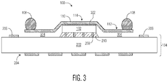
- FIG. 3 illustrates, in a simplified bottom-side-up cross-sectional view, the example semiconductor device package 100 at a subsequent stage of manufacture in accordance with an embodiment.
- the package 100 includes the thermal conductive structure 110 is mounted on the semiconductor die 102 and conductive connectors 108 are affixed on thermal conductive structure 110.
- the thermal conductive structure 110 includes the die pad portion 114 affixed to the backside of the semiconductor die 102 by way of a thermal conductive bonding material 302 (e.g., thermally conductive adhesive, solder, paste, epoxy, die attach film).
- the limb portions 112 extend laterally away from the die pad portion 114 and are downset forming a gap 304 between the limb portions 112 and the bottom surface of the package substrate 104.
- the gap 304 may be an air gap or filled with a low modulus material (e.g., for mechanical stability) or a thermally conductive material (e.g., for additional thermal conduction, dissipation), for example.
- the conductive connectors 108 are affixed at the distal ends of the limb portions 112. A region at the distal ends of the limb portions 112 may include features such as plating and/or dimples conducive for attachment of conductive connectors, for example.
- the conductive connectors 108 be any suitable conductive connector structures such as solder balls, gold studs, copper pillars, and the like. In some embodiments, conductive connectors 108 may be formed with enhanced thermal conductivity materials and/or structures.
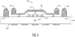
- FIG. 4 illustrates, in a simplified bottom-side-up cross-sectional view, the example semiconductor device package 100 at a subsequent stage of manufacture in accordance with an embodiment.
- the package 100 includes the thermal conductive structure 110 mounted on the semiconductor die 102 and conductive connectors 106 affixed on connector pads 206.
- the thermal conductive structure 110 is mounted on the semiconductor die 102
- the conductive connectors 106 are affixed on the respective connector pads 206.
- the conductive connectors 106 are coupled to provide input/output and power supply connections to the semiconductor die 102 by way of the connector pads 206.
- FIG. 5 and FIG. 6 illustrate, in simplified bottom-side-up cross-sectional views, the example semiconductor device package 100 taken along line A-A of FIG. 1 at alternative stages of manufacture in accordance with an embodiment.
- the embodiments depicted in FIG. 5 and FIG. 6 are subsequent to the stage of manufacture depicted in FIG. 2 and are alternatives to the embodiments depicted in FIG. 3 and FIG. 4 .
- FIG. 5 illustrates, in a simplified bottom-side-up cross-sectional view, the example semiconductor device package 100 at an alternative stage of manufacture in accordance with an embodiment.
- the package 100 includes the thermal conductive structure 110 mounted on the semiconductor die 102.
- the thermal conductive structure 110 includes the die pad portion 114 affixed to the backside of the semiconductor die 102 by way of a thermal conductive bonding material 502.
- the limb portions 112 extend laterally away from the die pad portion 114 and are downset forming a gap 504 between the limb portions 112 and the bottom surface of the package substrate 104.
- a region at the distal ends of the limb portions 112 are configured for attachment to a PCB by way of conductive connectors, for example.
- FIG. 6 illustrates, in a simplified bottom-side-up cross-sectional view, the example semiconductor device package 100 at an alternative stage of manufacture in accordance with an embodiment.
- the package 100 includes the thermal conductive structure 110 mounted on the semiconductor die 102 and conductive connectors 106 and 108 affixed on respective connector pads 206 and the thermal conductive structure 110.
- the thermal conductive structure 110 is mounted on the semiconductor die 102
- the conductive connectors 106 are affixed on the connector pads 206
- the conductive connectors 108 are affixed at the distal ends of the limb portions 112.
- the conductive connectors 106 are coupled to provide input/output and power supply connections to the semiconductor die 102 by way of the connector pads 206.
- FIG. 7 illustrates, in a simplified cross-sectional view, the example semiconductor device package 100 of FIG. 4 (and FIG. 6 ) as mounted on a PCB 702 in accordance with an embodiment.
- the package 100 is oriented (e.g., flipped), attached and interconnected to the PCB 702 by way of the conductive connectors 106 and 108.
- the conductive connectors 106 and 108 are affixed to respective pads 704 and 706 of the PCB 702.
- a thermal conduction path from the semiconductor die 102 is extended to the PCB by way of the conductive connectors 108 and the respective pads 706.
- an additional thermal conduction path may be formed between the semiconductor die 102 and a pad (not shown) formed on the PCB directly below the die pad portion 114. Because the thermal conduction path is formed at the bottom side of the package 100, the integrated conductive structure 204 at the top surface of the package substrate remains unobstructed.
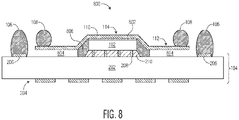
- FIG. 8 illustrates, in a simplified bottom-side-up cross-sectional view, an alternative example semiconductor device package 800 having a thermal dissipation feature in accordance with an embodiment.
- the package 800 includes a thermal conductive fillet 806 formed at the semiconductor die 102 to package substrate 104 transition.
- a thermally conductive material e.g., thermal epoxy, paste
- the thermally conductive material may be dispensed before or after the thermal conductive structure 110 is mounted on the semiconductor die 102 by way of a thermal conductive bonding material 802.
- the thermal conductive fillet 806 is configured and arranged to directly contact sidewalls of the semiconductor die 102 and the thermal conductive structure 110. In this arrangement, the limb portions 112 are further supported, and additional heat dissipation paths are formed from the sidewalls of the semiconductor die 102.
- a gap 804 remains between the limb portions 112 and the package substrate 104.
- the gap 804 may be an air gap or filled with a low modulus material (e.g., for additional mechanical stability) or a thermally conductive material (e.g., for additional thermal conduction, dissipation), for example. Because a thermal conduction path is formed (e.g., from the semiconductor die 102 to the conductive connector 108) at the bottom side of the package 800, the integrated conductive structure 204 at the top surface of the package substrate remains unobstructed.
- FIG. 9 illustrates, in a simplified bottom-side-up cross-sectional view, another alternative example semiconductor device package 900 having a thermal dissipation feature in accordance with an embodiment.
- the package 900 includes a thermal conductive structure 902 mounted on the semiconductor die 102 and conductive connectors 106 and 108 affixed on respective connector pads 206 and the thermal conductive structure 902.
- the thermal conductive structure 902 includes a die pad portion 912 affixed to the backside of the semiconductor die 102 by way of a thermal conductive bonding material 904.
- the thermal conductive structure 902 includes example thermal radiation fins 906 formed on the limb portions 910 and configured for additional heat dissipation.
- the thermal radiation fins 906 may be formed from similar materials (e.g., copper) as the thermal conductive structure 902, and formed in various suitable shapes and orientations.
- the outer-most surface of the thermal radiation fins 906 may be configured for direct contact with a PCB using a thermal paste, for example.
- the outer-most surface of the thermal radiation fins 906 may be configured for a direct solder connection with a PCB without using conductive connectors, for example. Because a thermal conduction path is formed (e.g., from the semiconductor die 102 to the conductive connector 108) at the bottom side of the package 800, the integrated conductive structure 204 at the top surface of the package substrate remains unobstructed.
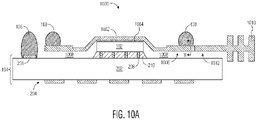
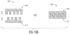
- FIG. 10A illustrates, in a simplified bottom-side-up cross-sectional view, an alternative example semiconductor device package 1000 configured with an external heatsink structure 1010 in accordance with an embodiment.
- the package 1000 includes a thermal conductive structure 1002 mounted on the semiconductor die 102 and attached to the external heatsink structure 1010.
- Conductive connectors 106 and 108 are affixed on respective connector pads 206 and the thermal conductive structure 1002.
- Cross-sectional views of an example interlocking connection structure taken along line B-B is depicted in FIG. 10B .
- the thermal conductive structure 1002 includes a die pad portion affixed to the backside of the semiconductor die 102 by way of a thermal conductive bonding material 1004. Limb portions of the thermal conductive structure 1002 extend laterally away from the die pad portion and are downset forming a gap 1008 between the limb portions and the package substrate 104.
- the thermal conductive structure 1002 includes an example interlocking connection structure portion 1006 formed at the distal ends of the limb portions and configured for attachment of the external heatsink structure 1010 for additional heat dissipation.
- the external heatsink structure 1010 When the external heatsink structure 1010 is joined with the thermal conductive structure 1002, a continuous thermal conduction path from the semiconductor die 102 to the external heatsink structure 1010 is formed.
- the external heatsink structure 1010 may be formed from a suitable metal (e.g., copper) having any suitable structure configured for heat dissipation.
- a thermal conduction path also extends to the PCB by way of the conductive connectors 108 affixed on the thermal conductive structure 1002. Because the thermal conduction paths are formed at the bottom side of the package 1000, the integrated conductive structure 204 at the top surface of the package substrate 104 remains unobstructed.
- connection structure portion 1006 of the thermal conductive structure 1002 and a corresponding interlocking connection structure portion 1012 of the external heatsink 1010 are depicted in an unmated arrangement 1020.
- the top side of the connection structure portion 1006 is configured for attachment to a PCB by way of conductive connectors 108, for example.
- the bottom side interlocking features may serve as a heatsink, for example, when an external heatsink is not attached.
- the corresponding interlocking connection structure portion 1012 formed on the external heatsink structure 1010 is configured for mating with the connection structure portion 1006.
- connection structure portion 1006 interlocked with the corresponding connection structure portion 1012 is depicted in a mated arrangement 1022.
- the example interlocking connection structure when in the mated arrangement 1022, ensures a sufficient thermal conduction.
- a thermal grease or paste applied on interlocking features may further increase the thermal conductivity of the interlocking connection structure.
- FIG. 11 illustrates, in a simplified bottom-side-up plan view, an example thermal conductive structure 1110 with a stress reducing feature in accordance with an embodiment.
- the thermal conductive structure 1110 depicted in FIG. 11 is an alternative to the thermal conductive structure 110 depicted in FIG. 1 .
- the thermal conductive structure 1110 is configured for attachment on a semiconductor die for improved heat dissipation.
- the thermal conductive structure 1110 includes a die pad portion 1114 and four limb portions 1112 extending laterally away from the die pad portion.
- the limb portions 1112 include a region formed at a distal end of each limb configured for attachment to a PCB by way of conductive connectors, for example.
- the thermal conductive structure 1110 when affixed to the semiconductor die, forms a thermal conduction and heat dissipation path between the semiconductor die and the conductive connectors.
- each limb portion 1112 includes a U-shaped stress relief feature 1116 formed between the die pad portion 1114 and the distal end of the limb portion 1112.
- the stress relief feature 1116 is configured to allow more flexibility in the limb portions 1112 after being affixed to a PCB, for example.
- the stress relief feature 1116 also provides more surface area for heat dissipation.
- the thermal conductive structure 1110 may be formed from suitable thermal conductive materials such as copper, silver, nickel, aluminum, and the like.
- the thermal conductive structure 1110 including the die pad portion 1114 and the limb portions 1112 may be formed from a stamped or etched metal sheet. For example, the thermal conductive structure 1110 may be manufactured in a manner consistent with the manufacture of a package leadframe.
- a semiconductor device package including a package substrate having a first major surface and a second major surface; a semiconductor die mounted on the first major surface of the package substrate; and a thermal conductive structure including a die pad portion affixed to the semiconductor die and a limb portion extending laterally away from the die pad portion, the limb portion located substantially over a portion of the package substrate, the thermal conductive structure configured to form a thermal conduction path between the semiconductor die and a distal end of the limb portion.
- a region at the distal end of the limb portion may be configured for attachment to a printed circuit board by way of a first conductive connector.
- the semiconductor device package may further include a connector pad at the first surface of the package substrate, the connector pad configured for attachment to the printed circuit board by way of a second conductive connector.
- the thermal conductive structure including the die pad portion and the limb portion may be formed from a stamped or etched metal sheet.
- the semiconductor device package may further include a thermal conductive fillet formed at the semiconductor die to package substrate transition, the fillet directly contacting sidewalls of the semiconductor die and the thermal conductive structure.
- the semiconductor device package may further include an antenna structure integrated at the second surface of the package substrate.
- the thermal conductive structure may further include one or more thermal conductive fins attached to the limb portion of the thermal conductive structure.
- the limb portion the thermal conductive structure may include a stress relief feature configured to reduce stress when the limb portion is attached to a printed circuit board.
- the distal end of the limb portion of the thermal conductive structure may be further configured for attachment of an external heatsink structure.
- a method including mounting a semiconductor die on a first surface of a package substrate; providing a thermal conductive structure including a die pad portion and a limb portion extending laterally away from the die pad portion; and affixing the die pad portion of the thermal conductive structure to the semiconductor die, the limb portion suspended over a portion of the package substrate.
- the method may further include affixing a first conductive connector at a distal end of the limb portion of the thermal conductive structure, the first conductive connector configured for attachment to a printed circuit board.
- the method may further include affixing a second conductive connector on a connector pad located at first surface of the package substrate, the second conductive connector configured for attachment to the printed circuit board.
- the package substrate may include an antenna structure integrated at a second surface of the package substrate.
- the method may further include forming a thermal conductive fillet at the semiconductor die to package substrate transition, the fillet directly contacting sidewalls of the semiconductor die and the thermal conductive structure.
- the limb portion of thermal conductive structure may be downset relative to the die pad portion of the thermal conductive structure.
- the affixing the die pad portion of the thermal conductive structure to the semiconductor die may include affixing the die pad portion to the semiconductor die by way of a thermally conductive adhesive or solder.
- a semiconductor device package including a package substrate having a first major surface and a second major surface; a semiconductor die having an active side and a backside, the active side mounted on the first major surface of the package substrate; and a thermal conductive structure having a die pad portion affixed to the backside of the semiconductor die and a limb portion extending laterally away from the die pad portion, the limb portion located substantially over a portion of the package substrate, a gap formed between the limb portion and the first major surface of the package substrate.
- the semiconductor device package may further include a first conductive connector affixed at a distal end of the limb portion and configured for attachment to a printed circuit board, a thermal conduction path formed between the semiconductor die and the first conductive connector.
- the semiconductor device package may further include a second conductive connector affixed on a connector pad at first surface of the package substrate, the second conductive connector configured for attachment to the printed circuit board.
- the first conductive connector and the second conductive connector may be characterized as balls of a ball grid array (BGA) package.
- BGA ball grid array
- a semiconductor device package having a thermal dissipation feature.
- An external thermal conductive structure is affixed to a semiconductor die to form the thermal dissipation structure at a bottom of the package.
- the external thermal conductive structure includes a die pad portion and a plurality of limb portion which extend over the package substrate.
- the bottom of the package is attached and interconnected with a printed circuit board by way of conductive connectors.
- the thermal conductive structure forms a thermal conduction path between the semiconductor die and the printed circuit board.
- an antenna structure integrated at the top surface of the package allows for propagation of radio signals, for example, while providing enhanced heat dissipation at the bottom surface of the package.
- Other features such as a package-on-package interface structure, surface mount technology structure, die bonding structure, shielding structure, and the like may be integrated at the top surface of the package.
Landscapes
- Cooling Or The Like Of Semiconductors Or Solid State Devices (AREA)
Abstract
Description
- This disclosure relates generally to semiconductor device packaging, and more specifically, to a semiconductor device package having thermal dissipation feature and method of forming the same.
- Today, there is an increasing trend to include sophisticated semiconductor devices in products and systems that are used every day. These sophisticated semiconductor devices often have sensitive circuitry and features that can be adversely affected by environmental conditions. For example, the performance of a semiconductor device may be degraded due to excessive heat accumulation. In extreme cases, a semiconductor device may be rendered non-functional due to excessive heat accumulation. Accordingly, there is a need to reduce or eliminate the effects of environmental conditions on such semiconductor devices.
- The present invention is set out in the appended set of claims.
- The present invention is illustrated by way of example and is not limited by the accompanying figures, in which like references indicate similar elements. Elements in the figures are illustrated for simplicity and clarity and have not necessarily been drawn to scale.
-
FIG. 1 illustrates, in a simplified bottom-side-up plan view, an example semiconductor device package having a thermal dissipation feature in accordance with an embodiment. -
FIG. 2 through FIG. 6 illustrate, in simplified cross-sectional views, the example semiconductor device package ofFIG. 1 at stages of manufacture in accordance with an embodiment. -
FIG. 7 illustrates, in a simplified cross-sectional view, the example semiconductor device package ofFIG. 6 as mounted on a printed circuit board (PCB) in accordance with an embodiment. -
FIG. 8 illustrates, in a simplified cross-sectional view, an alternative example semiconductor device package having a thermal dissipation feature in accordance with an embodiment. -
FIG. 9 illustrates, in a simplified cross-sectional view, another alternative example semiconductor device package having a thermal dissipation feature in accordance with an embodiment. -
FIG. 10A andFIG. 10B illustrate, in simplified cross-sectional views, an alternative example semiconductor device package configured with an external heatsink in accordance with an embodiment. -
FIG. 11 illustrates, in a simplified bottom-side-up plan view, an example thermal conductive structure with a stress reducing feature in accordance with an embodiment. - Generally, there is provided, a semiconductor device package having a thermal dissipation feature. An external thermal conductive structure is affixed to a semiconductor die to form the thermal dissipation structure at a bottom of the package. The external thermal conductive structure includes a die pad portion and a plurality of limb portions which extend over the package substrate. The bottom of the package is attached and interconnected with a printed circuit board by way of conductive connectors. The thermal conductive structure forms a thermal conduction path between the semiconductor die and the printed circuit board. With the thermal conductive structure affixed at the bottom of the package, a top surface of the package remains unobstructed. Accordingly, an antenna structure integrated at the top surface of the package allows for propagation of radio signals, for example, while providing enhanced heat dissipation at the bottom surface of the package. Other features such as a package-on-package interface structure, surface mount technology structure, die bonding structure, shielding structure, and the like may be integrated at the top surface of the package.
-
FIG. 1 illustrates, in a simplified bottom-side-up plan view, an examplesemiconductor device package 100 having a thermal dissipation feature in accordance with an embodiment. Thepackage 100 includes asemiconductor die 102 mounted on apackage substrate 104 havingconductive connectors conductive structure 110 affixed on the semiconductor die 102. In this embodiment, the thermalconductive structure 110 includes adie pad portion 114 and fourlimb portions 112 extending laterally away from the die pad portion and suspended over portions of thepackage substrate 104. Thelimb portions 112 include a region formed at a distal end of each limb configured for attachment to a printed circuit board (PCB) by way ofconductive connectors 108, for example. Cross-sectional views of examples of thesemiconductor device package 100 having a thermal dissipation feature taken along line A-A at stages of manufacture are depicted inFIG. 2 through FIG. 6 . - The semiconductor die 102 has an active side (e.g., major side having circuitry, bond pads) and a backside (e.g., major side opposite of the active surface). As depicted in the bottom-side-up plan view of
FIG. 1 , the active side of thesemiconductor die 102 is mounted on thepackage substrate 104 and interconnected utilizing bond pads (not shown) at the active side, for example. In this embodiment, the semiconductor die 102 is configured in a flip-chip orientation having the active side mounted on the package substrate 104.Thesemiconductor die 102 may be formed from any suitable semiconductor material, such as silicon, germanium, gallium arsenide, gallium nitride, and the like. Semiconductor die 102 may further include any digital circuits, analog circuits, RF circuits, memory, processor, the like, and combinations thereof at the active surface. - The
package substrate 104 has a top surface and a bottom surface (e.g., major surface opposite of the top surface). As depicted in the bottom-side-up plan view ofFIG. 1 , the active side of thesemiconductor die 102 andconductive connectors package substrate 104, for example. Theconductive connectors 106 may be characterized as input/output and power supply connectors whereas theconductive connectors 108 may be characterized as thermal conduction and heat dissipation path connectors. In some embodiments, theconductive connectors 108 may be configured for connection to a ground power supply, for example, in addition to being part of a thermal conduction and heat dissipation path. Theconductive connectors conductive connectors package substrate 104 is formed as a multi-layer laminate structure having conductive features (e.g., metal traces, pads) separated by non-conductive material (e.g., FR-4). In this embodiment, thepackage substrate 104 is characterized as a chip scale package (CSP) type package substrate. - The thermal
conductive structure 110 affixed to the semiconductor die 102 forms a thermal conduction and heat dissipation path between the semiconductor die 102 andconductive connectors 108. The thermalconductive structure 110 may be formed from suitable thermal conductive materials such as copper, silver, nickel, aluminum, and the like. The thermalconductive structure 110 including thedie pad portion 114 and thelimb portions 112 may be formed from a stamped or etched metal sheet. For example, the thermalconductive structure 110 may be manufactured in a manner consistent with the manufacture of a package leadframe. The thermalconductive structure 110 may be affixed to thesemiconductor die 102 by way of a thermally conductive adhesive or solder, for example. The thermalconductive structure 110 may be affixed to thesemiconductor die 102 of packages while in an array (e.g., strip) form or in singulated form. -
FIG. 2 through FIG. 6 illustrate, in simplified cross-sectional views, the examplesemiconductor device package 100 taken along line A-A ofFIG. 1 at stages of manufacture in accordance with an embodiment. -
FIG. 2 illustrates, in a simplified bottom-side-up cross-sectional view, the examplesemiconductor device package 100 at a stage of manufacture in accordance with an embodiment. At this stage, thepackage 100 includes the active side of thesemiconductor die 102 interconnected with the bottom surface of thepackage substrate 104 by way ofconductive die connectors 208 and underfilled with anepoxy material 210. The dieconnectors 208 may be any suitable die connector structure such as solder bumps, gold studs, copper pillars, and the like. Features such as bond pads on thesemiconductor die 102 and corresponding pads on thepackage substrate 104 are not shown for illustration purposes. - The
package substrate 104 is formed as a multi-layer laminate structure having conductive features separated by a non-conductive material. In this embodiment, thepackage substate 104 includesconnector pads 206 located at the bottom surface and aconductive structure 204 integrated at the top surface of thepackage substrate 104. In this embodiment, the integratedconductive structure 204 is characterized as an antenna structure configured for propagation of radio frequency (RF) signals such as a radar, Wi-Fi, UWB, 5G and 6G signals, for example. In other embodiments, the integratedconductive structure 204 may include features such as a package-on-package (PoP) interface structure, surface mount technology structure, die bonding structure, shielding structure, and the like integrated at the top surface of thepackage substrate 104. Theconnector pads 206 and the integratedconductive structure 204 are separated by anon-conductive material 202. Theconnector pads 206 and the integratedconductive structure 204 may be formed from a suitable metal such as copper, for example. Interconnect features such as conductive vias and traces embedded in thepackage substrate 104 are not shown for illustration purposes. -
FIG. 3 illustrates, in a simplified bottom-side-up cross-sectional view, the examplesemiconductor device package 100 at a subsequent stage of manufacture in accordance with an embodiment. At this stage, thepackage 100 includes the thermalconductive structure 110 is mounted on the semiconductor die 102 andconductive connectors 108 are affixed on thermalconductive structure 110. In this embodiment, the thermalconductive structure 110 includes thedie pad portion 114 affixed to the backside of the semiconductor die 102 by way of a thermal conductive bonding material 302 (e.g., thermally conductive adhesive, solder, paste, epoxy, die attach film). Thelimb portions 112 extend laterally away from thedie pad portion 114 and are downset forming agap 304 between thelimb portions 112 and the bottom surface of thepackage substrate 104. Thegap 304 may be an air gap or filled with a low modulus material (e.g., for mechanical stability) or a thermally conductive material (e.g., for additional thermal conduction, dissipation), for example. Theconductive connectors 108 are affixed at the distal ends of thelimb portions 112. A region at the distal ends of thelimb portions 112 may include features such as plating and/or dimples conducive for attachment of conductive connectors, for example. Theconductive connectors 108 be any suitable conductive connector structures such as solder balls, gold studs, copper pillars, and the like. In some embodiments,conductive connectors 108 may be formed with enhanced thermal conductivity materials and/or structures. -
FIG. 4 illustrates, in a simplified bottom-side-up cross-sectional view, the examplesemiconductor device package 100 at a subsequent stage of manufacture in accordance with an embodiment. At this stage, thepackage 100 includes the thermalconductive structure 110 mounted on the semiconductor die 102 andconductive connectors 106 affixed onconnector pads 206. After the thermalconductive structure 110 is mounted on the semiconductor die 102, theconductive connectors 106 are affixed on therespective connector pads 206. In this embodiment, theconductive connectors 106 are coupled to provide input/output and power supply connections to the semiconductor die 102 by way of theconnector pads 206. -
FIG. 5 andFIG. 6 illustrate, in simplified bottom-side-up cross-sectional views, the examplesemiconductor device package 100 taken along line A-A ofFIG. 1 at alternative stages of manufacture in accordance with an embodiment. The embodiments depicted inFIG. 5 andFIG. 6 are subsequent to the stage of manufacture depicted inFIG. 2 and are alternatives to the embodiments depicted inFIG. 3 andFIG. 4 . -
FIG. 5 illustrates, in a simplified bottom-side-up cross-sectional view, the examplesemiconductor device package 100 at an alternative stage of manufacture in accordance with an embodiment. At this stage, thepackage 100 includes the thermalconductive structure 110 mounted on the semiconductor die 102. In this embodiment, the thermalconductive structure 110 includes thedie pad portion 114 affixed to the backside of the semiconductor die 102 by way of a thermalconductive bonding material 502. Thelimb portions 112 extend laterally away from thedie pad portion 114 and are downset forming agap 504 between thelimb portions 112 and the bottom surface of thepackage substrate 104. A region at the distal ends of thelimb portions 112 are configured for attachment to a PCB by way of conductive connectors, for example. -
FIG. 6 illustrates, in a simplified bottom-side-up cross-sectional view, the examplesemiconductor device package 100 at an alternative stage of manufacture in accordance with an embodiment. At this stage, thepackage 100 includes the thermalconductive structure 110 mounted on the semiconductor die 102 andconductive connectors respective connector pads 206 and the thermalconductive structure 110. After the thermalconductive structure 110 is mounted on the semiconductor die 102, theconductive connectors 106 are affixed on theconnector pads 206 and theconductive connectors 108 are affixed at the distal ends of thelimb portions 112. In this embodiment, theconductive connectors 106 are coupled to provide input/output and power supply connections to the semiconductor die 102 by way of theconnector pads 206. -
FIG. 7 illustrates, in a simplified cross-sectional view, the examplesemiconductor device package 100 ofFIG. 4 (andFIG. 6 ) as mounted on aPCB 702 in accordance with an embodiment. In this embodiment, thepackage 100 is oriented (e.g., flipped), attached and interconnected to thePCB 702 by way of theconductive connectors conductive connectors respective pads PCB 702. In this embodiment, a thermal conduction path from the semiconductor die 102 is extended to the PCB by way of theconductive connectors 108 and therespective pads 706. In some embodiments, an additional thermal conduction path may be formed between the semiconductor die 102 and a pad (not shown) formed on the PCB directly below thedie pad portion 114. Because the thermal conduction path is formed at the bottom side of thepackage 100, the integratedconductive structure 204 at the top surface of the package substrate remains unobstructed. -
FIG. 8 illustrates, in a simplified bottom-side-up cross-sectional view, an alternative examplesemiconductor device package 800 having a thermal dissipation feature in accordance with an embodiment. At this stage, thepackage 800 includes a thermalconductive fillet 806 formed at the semiconductor die 102 to packagesubstrate 104 transition. A thermally conductive material (e.g., thermal epoxy, paste) is dispensed around a perimeter of the semiconductor die 102 such that a fillet is formed at the semiconductor die 102 to packagesubstrate 104 transition. The thermally conductive material may be dispensed before or after the thermalconductive structure 110 is mounted on the semiconductor die 102 by way of a thermalconductive bonding material 802. The thermalconductive fillet 806 is configured and arranged to directly contact sidewalls of the semiconductor die 102 and the thermalconductive structure 110. In this arrangement, thelimb portions 112 are further supported, and additional heat dissipation paths are formed from the sidewalls of the semiconductor die 102. Agap 804 remains between thelimb portions 112 and thepackage substrate 104. In some embodiments, thegap 804 may be an air gap or filled with a low modulus material (e.g., for additional mechanical stability) or a thermally conductive material (e.g., for additional thermal conduction, dissipation), for example. Because a thermal conduction path is formed (e.g., from the semiconductor die 102 to the conductive connector 108) at the bottom side of thepackage 800, the integratedconductive structure 204 at the top surface of the package substrate remains unobstructed. -
FIG. 9 illustrates, in a simplified bottom-side-up cross-sectional view, another alternative examplesemiconductor device package 900 having a thermal dissipation feature in accordance with an embodiment. At this stage, thepackage 900 includes a thermalconductive structure 902 mounted on the semiconductor die 102 andconductive connectors respective connector pads 206 and the thermalconductive structure 902. In this embodiment, the thermalconductive structure 902 includes adie pad portion 912 affixed to the backside of the semiconductor die 102 by way of a thermalconductive bonding material 904.Limb portions 910 of the thermalconductive structure 902 extend laterally away from thedie pad portion 912 and are downset forming agap 908 between thelimb portions 910 and thepackage substrate 104. In this embodiment, the thermalconductive structure 902 includes examplethermal radiation fins 906 formed on thelimb portions 910 and configured for additional heat dissipation. Thethermal radiation fins 906 may be formed from similar materials (e.g., copper) as the thermalconductive structure 902, and formed in various suitable shapes and orientations. In some embodiments, the outer-most surface of thethermal radiation fins 906 may be configured for direct contact with a PCB using a thermal paste, for example. In some embodiments, the outer-most surface of thethermal radiation fins 906 may be configured for a direct solder connection with a PCB without using conductive connectors, for example. Because a thermal conduction path is formed (e.g., from the semiconductor die 102 to the conductive connector 108) at the bottom side of thepackage 800, the integratedconductive structure 204 at the top surface of the package substrate remains unobstructed. -
FIG. 10A illustrates, in a simplified bottom-side-up cross-sectional view, an alternative examplesemiconductor device package 1000 configured with anexternal heatsink structure 1010 in accordance with an embodiment. At this stage, thepackage 1000 includes a thermalconductive structure 1002 mounted on the semiconductor die 102 and attached to theexternal heatsink structure 1010.Conductive connectors respective connector pads 206 and the thermalconductive structure 1002. Cross-sectional views of an example interlocking connection structure taken along line B-B is depicted inFIG. 10B . - In the embodiment depicted in
FIG. 10A , the thermalconductive structure 1002 includes a die pad portion affixed to the backside of the semiconductor die 102 by way of a thermalconductive bonding material 1004. Limb portions of the thermalconductive structure 1002 extend laterally away from the die pad portion and are downset forming agap 1008 between the limb portions and thepackage substrate 104. In this embodiment, the thermalconductive structure 1002 includes an example interlockingconnection structure portion 1006 formed at the distal ends of the limb portions and configured for attachment of theexternal heatsink structure 1010 for additional heat dissipation. When theexternal heatsink structure 1010 is joined with the thermalconductive structure 1002, a continuous thermal conduction path from the semiconductor die 102 to theexternal heatsink structure 1010 is formed. Theexternal heatsink structure 1010 may be formed from a suitable metal (e.g., copper) having any suitable structure configured for heat dissipation. In this embodiment, a thermal conduction path also extends to the PCB by way of theconductive connectors 108 affixed on the thermalconductive structure 1002. Because the thermal conduction paths are formed at the bottom side of thepackage 1000, the integratedconductive structure 204 at the top surface of thepackage substrate 104 remains unobstructed. - The example interlocking connection structure taken along line B-B is shown in more detail in
FIG. 10B . Theconnection structure portion 1006 of the thermalconductive structure 1002 and a corresponding interlockingconnection structure portion 1012 of theexternal heatsink 1010 are depicted in anunmated arrangement 1020. The top side of theconnection structure portion 1006 is configured for attachment to a PCB by way ofconductive connectors 108, for example. The bottom side interlocking features may serve as a heatsink, for example, when an external heatsink is not attached. The corresponding interlockingconnection structure portion 1012 formed on theexternal heatsink structure 1010 is configured for mating with theconnection structure portion 1006. Theconnection structure portion 1006 interlocked with the correspondingconnection structure portion 1012 is depicted in a matedarrangement 1022. The example interlocking connection structure, when in the matedarrangement 1022, ensures a sufficient thermal conduction. A thermal grease or paste applied on interlocking features may further increase the thermal conductivity of the interlocking connection structure. -
FIG. 11 illustrates, in a simplified bottom-side-up plan view, an example thermalconductive structure 1110 with a stress reducing feature in accordance with an embodiment. The thermalconductive structure 1110 depicted inFIG. 11 is an alternative to the thermalconductive structure 110 depicted inFIG. 1 . The thermalconductive structure 1110 is configured for attachment on a semiconductor die for improved heat dissipation. In this embodiment, the thermalconductive structure 1110 includes adie pad portion 1114 and fourlimb portions 1112 extending laterally away from the die pad portion. Thelimb portions 1112 include a region formed at a distal end of each limb configured for attachment to a PCB by way of conductive connectors, for example. The thermalconductive structure 1110, when affixed to the semiconductor die, forms a thermal conduction and heat dissipation path between the semiconductor die and the conductive connectors. - In this embodiment, each
limb portion 1112 includes a U-shapedstress relief feature 1116 formed between thedie pad portion 1114 and the distal end of thelimb portion 1112. Thestress relief feature 1116 is configured to allow more flexibility in thelimb portions 1112 after being affixed to a PCB, for example. Thestress relief feature 1116 also provides more surface area for heat dissipation. The thermalconductive structure 1110 may be formed from suitable thermal conductive materials such as copper, silver, nickel, aluminum, and the like. The thermalconductive structure 1110 including thedie pad portion 1114 and thelimb portions 1112 may be formed from a stamped or etched metal sheet. For example, the thermalconductive structure 1110 may be manufactured in a manner consistent with the manufacture of a package leadframe. - Generally, there is provided, a semiconductor device package including a package substrate having a first major surface and a second major surface; a semiconductor die mounted on the first major surface of the package substrate; and a thermal conductive structure including a die pad portion affixed to the semiconductor die and a limb portion extending laterally away from the die pad portion, the limb portion located substantially over a portion of the package substrate, the thermal conductive structure configured to form a thermal conduction path between the semiconductor die and a distal end of the limb portion. A region at the distal end of the limb portion may be configured for attachment to a printed circuit board by way of a first conductive connector. The semiconductor device package may further include a connector pad at the first surface of the package substrate, the connector pad configured for attachment to the printed circuit board by way of a second conductive connector. The thermal conductive structure including the die pad portion and the limb portion may be formed from a stamped or etched metal sheet. The semiconductor device package may further include a thermal conductive fillet formed at the semiconductor die to package substrate transition, the fillet directly contacting sidewalls of the semiconductor die and the thermal conductive structure. The semiconductor device package may further include an antenna structure integrated at the second surface of the package substrate. The thermal conductive structure may further include one or more thermal conductive fins attached to the limb portion of the thermal conductive structure. The limb portion the thermal conductive structure may include a stress relief feature configured to reduce stress when the limb portion is attached to a printed circuit board. The distal end of the limb portion of the thermal conductive structure may be further configured for attachment of an external heatsink structure.
- In another embodiment, there is provided, a method including mounting a semiconductor die on a first surface of a package substrate; providing a thermal conductive structure including a die pad portion and a limb portion extending laterally away from the die pad portion; and affixing the die pad portion of the thermal conductive structure to the semiconductor die, the limb portion suspended over a portion of the package substrate. The method may further include affixing a first conductive connector at a distal end of the limb portion of the thermal conductive structure, the first conductive connector configured for attachment to a printed circuit board. The method may further include affixing a second conductive connector on a connector pad located at first surface of the package substrate, the second conductive connector configured for attachment to the printed circuit board. The package substrate may include an antenna structure integrated at a second surface of the package substrate. The method may further include forming a thermal conductive fillet at the semiconductor die to package substrate transition, the fillet directly contacting sidewalls of the semiconductor die and the thermal conductive structure. The limb portion of thermal conductive structure may be downset relative to the die pad portion of the thermal conductive structure. The affixing the die pad portion of the thermal conductive structure to the semiconductor die may include affixing the die pad portion to the semiconductor die by way of a thermally conductive adhesive or solder.
- In yet another embodiment, there is provided, a semiconductor device package including a package substrate having a first major surface and a second major surface; a semiconductor die having an active side and a backside, the active side mounted on the first major surface of the package substrate; and a thermal conductive structure having a die pad portion affixed to the backside of the semiconductor die and a limb portion extending laterally away from the die pad portion, the limb portion located substantially over a portion of the package substrate, a gap formed between the limb portion and the first major surface of the package substrate. The semiconductor device package may further include a first conductive connector affixed at a distal end of the limb portion and configured for attachment to a printed circuit board, a thermal conduction path formed between the semiconductor die and the first conductive connector. The semiconductor device package may further include a second conductive connector affixed on a connector pad at first surface of the package substrate, the second conductive connector configured for attachment to the printed circuit board. The first conductive connector and the second conductive connector may be characterized as balls of a ball grid array (BGA) package.
- By now, it should be appreciated that there has been provided a semiconductor device package having a thermal dissipation feature. An external thermal conductive structure is affixed to a semiconductor die to form the thermal dissipation structure at a bottom of the package. The external thermal conductive structure includes a die pad portion and a plurality of limb portion which extend over the package substrate. The bottom of the package is attached and interconnected with a printed circuit board by way of conductive connectors. The thermal conductive structure forms a thermal conduction path between the semiconductor die and the printed circuit board. With the thermal conductive structure affixed at the bottom of the package, a top surface of the package remains unobstructed. Accordingly, an antenna structure integrated at the top surface of the package allows for propagation of radio signals, for example, while providing enhanced heat dissipation at the bottom surface of the package. Other features such as a package-on-package interface structure, surface mount technology structure, die bonding structure, shielding structure, and the like may be integrated at the top surface of the package.
- The terms "front," "back," "top," "bottom," "over," "under" and the like in the description and in the claims, if any, are used for descriptive purposes and not necessarily for describing permanent relative positions. It is understood that the terms so used are interchangeable under appropriate circumstances such that the embodiments of the invention described herein are, for example, capable of operation in other orientations than those illustrated or otherwise described herein.
- Although the invention is described herein with reference to specific embodiments, various modifications and changes can be made without departing from the scope of the present invention as set forth in the claims below. Accordingly, the specification and figures are to be regarded in an illustrative rather than a restrictive sense, and all such modifications are intended to be included within the scope of the present invention. Any benefits, advantages, or solutions to problems that are described herein with regard to specific embodiments are not intended to be construed as a critical, required, or essential feature or element of any or all the claims.
- Furthermore, the terms "a" or "an," as used herein, are defined as one or more than one. Also, the use of introductory phrases such as "at least one" and "one or more" in the claims should not be construed to imply that the introduction of another claim element by the indefinite articles "a" or "an" limits any particular claim containing such introduced claim element to inventions containing only one such element, even when the same claim includes the introductory phrases "one or more" or "at least one" and indefinite articles such as "a" or "an." The same holds true for the use of definite articles.
- Unless stated otherwise, terms such as "first" and "second" are used to arbitrarily distinguish between the elements such terms describe. Thus, these terms are not necessarily intended to indicate temporal or other prioritization of such elements.
Claims (15)
- A semiconductor device package comprising:a package substrate having a first major surface and a second major surface;a semiconductor die mounted on the first major surface of the package substrate; anda thermal conductive structure including a die pad portion affixed to the semiconductor die and a limb portion extending laterally away from the die pad portion, the limb portion located substantially over a portion of the package substrate, the thermal conductive structure configured to form a thermal conduction path between the semiconductor die and a distal end of the limb portion.
- The semiconductor device package of claim 1, wherein a region at the distal end of the limb portion is configured for attachment to a printed circuit board by way of a first conductive connector.
- The semiconductor device package of claim 1 or 2, further comprising a connector pad at the first surface of the package substrate, the connector pad configured for attachment to the printed circuit board by way of a second conductive connector.
- The semiconductor device package of any of the claims 1 to 3, wherein the thermal conductive structure including the die pad portion and the limb portion is formed from a stamped or etched metal sheet.
- The semiconductor device package of any of the claims 1 to 4, further comprising a thermal conductive fillet formed at the semiconductor die to package substrate transition, the fillet directly contacting sidewalls of the semiconductor die and the thermal conductive structure.
- The semiconductor device package of any of the claims 1 to 5, further comprising an antenna structure integrated at the second surface of the package substrate.
- The semiconductor device package of any of the claims 1 to 6, wherein the thermal conductive structure further comprises one or more thermal conductive fins attached to the limb portion of the thermal conductive structure.
- The semiconductor device package of any of the claims 1 to 7, wherein the limb portion of the thermal conductive structure includes a stress relief feature configured to reduce stress when the limb portion is attached to a printed circuit board.
- The semiconductor device package of any of the claims 1 to 8, wherein the distal end of the limb portion of the thermal conductive structure is further configured for attachment of an external heatsink structure.
- A method comprising:mounting a semiconductor die on a first surface of a package substrate;providing a thermal conductive structure including a die pad portion and a limb portion extending laterally away from the die pad portion; andaffixing the die pad portion of the thermal conductive structure to the semiconductor die, the limb portion suspended over a portion of the package substrate.
- The method of claim 10, further comprising affixing a first conductive connector at a distal end of the limb portion of the thermal conductive structure, the first conductive connector configured for attachment to a printed circuit board.
- The method of claim 10 or 11, further comprising affixing a second conductive connector on a connector pad located at first surface of the package substrate, the second conductive connector configured for attachment to the printed circuit board.
- The method of any of the claims 10 to 12, wherein the package substrate includes an antenna structure integrated at a second surface of the package substrate.
- The method of any of the claims 10 to 13, further comprising forming a thermal conductive fillet at the semiconductor die to package substrate transition, the fillet directly contacting sidewalls of the semiconductor die and the thermal conductive structure.
- The method of any of the claims 10 to 14, wherein the limb portion of thermal conductive structure is downset relative to the die pad portion of the thermal conductive structure.
Applications Claiming Priority (1)
| Application Number | Priority Date | Filing Date | Title |
|---|---|---|---|
| US17/241,156 US12406896B2 (en) | 2021-04-27 | 2021-04-27 | Semiconductor device package having thermal dissipation feature and method therefor |
Publications (1)
| Publication Number | Publication Date |
|---|---|
| EP4084059A1 true EP4084059A1 (en) | 2022-11-02 |
Family
ID=81326672
Family Applications (1)
| Application Number | Title | Priority Date | Filing Date |
|---|---|---|---|
| EP22168665.2A Pending EP4084059A1 (en) | 2021-04-27 | 2022-04-15 | Semiconductor device package having thermal dissipation feature and method therefor |
Country Status (2)
| Country | Link |
|---|---|
| US (1) | US12406896B2 (en) |
| EP (1) | EP4084059A1 (en) |
Families Citing this family (2)
| Publication number | Priority date | Publication date | Assignee | Title |
|---|---|---|---|---|
| US12557646B2 (en) * | 2022-08-31 | 2026-02-17 | Taiwan Semiconductor Manufacturing Company, Ltd. | Multi-die package and methods of formation |
| CN117894783B (en) * | 2023-12-22 | 2026-05-12 | 泉州市三安集成电路有限公司 | Semiconductor packaging structure |
Citations (10)
| Publication number | Priority date | Publication date | Assignee | Title |
|---|---|---|---|---|
| US20030214049A1 (en) * | 2002-05-16 | 2003-11-20 | Hortaleza Edgardo R. | Heat dissipating flip-chip ball grid array |
| US20050112796A1 (en) * | 2003-11-24 | 2005-05-26 | Ararao Virgil C. | Semiconductor package heat spreaders and fabrication methods therefor |
| US20080291115A1 (en) * | 2007-05-22 | 2008-11-27 | Sibeam, Inc. | Surface mountable integrated circuit packaging scheme |
| US20090045505A1 (en) * | 2007-08-15 | 2009-02-19 | Via Technologies, Inc. | Electronic device with package module |
| US20120126396A1 (en) * | 2010-11-19 | 2012-05-24 | Broadcom Corporation | Die down device with thermal connector |
| US9673175B1 (en) * | 2015-08-25 | 2017-06-06 | Freescale Semiconductor,Inc. | Heat spreader for package-on-package (PoP) type packages |
| WO2017222471A1 (en) * | 2016-06-24 | 2017-12-28 | Agency For Science, Technology And Research | Semiconductor package and method of forming the same |
| EP3690935A1 (en) * | 2019-01-30 | 2020-08-05 | MediaTek Inc. | Semiconductor package having improved thermal interface between semiconductor die and heat spreading structure |
| US20210280507A1 (en) * | 2020-03-05 | 2021-09-09 | Qualcomm Incorporated | Package comprising dummy interconnects |
| US20220181230A1 (en) * | 2020-12-07 | 2022-06-09 | Nxp Usa, Inc. | Semiconductor device package having thermal dissipation feature and method therefor |
Family Cites Families (17)
| Publication number | Priority date | Publication date | Assignee | Title |
|---|---|---|---|---|
| US6146921A (en) * | 1998-09-16 | 2000-11-14 | Intel Corporation | Cavity mold cap BGA package with post mold thermally conductive epoxy attach heat sink |
| US6255143B1 (en) | 1999-08-04 | 2001-07-03 | St. Assembly Test Services Pte Ltd. | Flip chip thermally enhanced ball grid array |
| US6504723B1 (en) * | 2001-11-15 | 2003-01-07 | Intel Corporation | Electronic assembly having solder thermal interface between a die substrate and a heat spreader |
| US7064426B2 (en) | 2002-09-17 | 2006-06-20 | Chippac, Inc. | Semiconductor multi-package module having wire bond interconnect between stacked packages |
| TWI286832B (en) * | 2002-11-05 | 2007-09-11 | Advanced Semiconductor Eng | Thermal enhance semiconductor package |
| US7205651B2 (en) * | 2004-04-16 | 2007-04-17 | St Assembly Test Services Ltd. | Thermally enhanced stacked die package and fabrication method |
| US7362580B2 (en) * | 2004-06-18 | 2008-04-22 | Intel Corporation | Electronic assembly having an indium wetting layer on a thermally conductive body |
| TWI263256B (en) * | 2005-05-03 | 2006-10-01 | Siliconware Precision Industries Co Ltd | Flip-chip semiconductor device |
| US7355289B2 (en) | 2005-07-29 | 2008-04-08 | Freescale Semiconductor, Inc. | Packaged integrated circuit with enhanced thermal dissipation |
| US7361972B2 (en) | 2006-03-20 | 2008-04-22 | Taiwan Semiconductor Manufacturing Co., Ltd. | Chip packaging structure for improving reliability |
| JP2011082345A (en) * | 2009-10-07 | 2011-04-21 | Panasonic Corp | Semiconductor device |
| US8786076B2 (en) | 2011-03-21 | 2014-07-22 | Stats Chippac, Ltd. | Semiconductor device and method of forming a thermally reinforced semiconductor die |
| US9190297B2 (en) * | 2011-08-11 | 2015-11-17 | Stats Chippac, Ltd. | Semiconductor device and method of forming a stackable semiconductor package with vertically-oriented discrete electrical devices as interconnect structures |
| US9305854B2 (en) | 2012-08-21 | 2016-04-05 | Stats Chippac, Ltd. | Semiconductor device and method of forming RDL using UV-cured conductive ink over wafer level package |
| US9355985B2 (en) | 2014-05-30 | 2016-05-31 | Freescale Semiconductor, Inc. | Microelectronic packages having sidewall-deposited heat spreader structures and methods for the fabrication thereof |
| US9842818B2 (en) | 2016-03-28 | 2017-12-12 | Intel Corporation | Variable ball height on ball grid array packages by solder paste transfer |
| WO2018182653A1 (en) | 2017-03-30 | 2018-10-04 | Intel Corporation | Rfic having coaxial interconnect and molded layer |
-
2021
- 2021-04-27 US US17/241,156 patent/US12406896B2/en active Active
-
2022
- 2022-04-15 EP EP22168665.2A patent/EP4084059A1/en active Pending
Patent Citations (10)
| Publication number | Priority date | Publication date | Assignee | Title |
|---|---|---|---|---|
| US20030214049A1 (en) * | 2002-05-16 | 2003-11-20 | Hortaleza Edgardo R. | Heat dissipating flip-chip ball grid array |
| US20050112796A1 (en) * | 2003-11-24 | 2005-05-26 | Ararao Virgil C. | Semiconductor package heat spreaders and fabrication methods therefor |
| US20080291115A1 (en) * | 2007-05-22 | 2008-11-27 | Sibeam, Inc. | Surface mountable integrated circuit packaging scheme |
| US20090045505A1 (en) * | 2007-08-15 | 2009-02-19 | Via Technologies, Inc. | Electronic device with package module |
| US20120126396A1 (en) * | 2010-11-19 | 2012-05-24 | Broadcom Corporation | Die down device with thermal connector |
| US9673175B1 (en) * | 2015-08-25 | 2017-06-06 | Freescale Semiconductor,Inc. | Heat spreader for package-on-package (PoP) type packages |
| WO2017222471A1 (en) * | 2016-06-24 | 2017-12-28 | Agency For Science, Technology And Research | Semiconductor package and method of forming the same |
| EP3690935A1 (en) * | 2019-01-30 | 2020-08-05 | MediaTek Inc. | Semiconductor package having improved thermal interface between semiconductor die and heat spreading structure |
| US20210280507A1 (en) * | 2020-03-05 | 2021-09-09 | Qualcomm Incorporated | Package comprising dummy interconnects |
| US20220181230A1 (en) * | 2020-12-07 | 2022-06-09 | Nxp Usa, Inc. | Semiconductor device package having thermal dissipation feature and method therefor |
Also Published As
| Publication number | Publication date |
|---|---|
| US20220344235A1 (en) | 2022-10-27 |
| US12406896B2 (en) | 2025-09-02 |
Similar Documents
| Publication | Publication Date | Title |
|---|---|---|
| EP3690935B1 (en) | Semiconductor package having improved thermal interface between semiconductor die and heat spreading structure | |
| US6873032B1 (en) | Thermally enhanced chip scale lead on chip semiconductor package and method of making same | |
| US6657311B1 (en) | Heat dissipating flip-chip ball grid array | |
| US7514771B2 (en) | Leadless lead-frame | |
| US20060249852A1 (en) | Flip-chip semiconductor device | |
| KR100698526B1 (en) | A wiring board having a heat dissipation layer and a semiconductor package using the same | |
| JPH0964099A (en) | Semiconductor device and its mounting structure | |
| US7002246B2 (en) | Chip package structure with dual heat sinks | |
| US7045883B1 (en) | Thermally enhanced chip scale lead on chip semiconductor package and method of making same | |
| US7224057B2 (en) | Thermal enhance package with universal heat spreader | |
| US20250300036A1 (en) | Semiconductor device | |
| CN113272953A (en) | Semiconductor package | |
| JP2006505945A (en) | Folded flex, wireless bonding, multi-chip power package | |
| US12406896B2 (en) | Semiconductor device package having thermal dissipation feature and method therefor | |
| US11817366B2 (en) | Semiconductor device package having thermal dissipation feature and method therefor | |
| US7064009B1 (en) | Thermally enhanced chip scale lead on chip semiconductor package and method of making same | |
| EP4632809A1 (en) | Semiconductor device with embedded flex substrate and method therefor | |
| EP4593080A1 (en) | Semiconductor device with dual downset leadframe and method therefor | |
| JP3618393B2 (en) | Ball grid array integrated circuit package with high thermal conductivity | |
| US6963129B1 (en) | Multi-chip package having a contiguous heat spreader assembly | |
| US20070284709A1 (en) | Semiconductor Device with Improved High Current Performance | |
| US7019410B1 (en) | Die attach material for TBGA or flexible circuitry | |
| EP4513533A1 (en) | Semiconductor device with embedded leadframe and method therefor | |
| WO2007051101A2 (en) | Closed loop thermally enhanced flip chip bga | |
| EP4557353A2 (en) | Semiconductor device having integrated lid structure and method therefor |
Legal Events
| Date | Code | Title | Description |
|---|---|---|---|
| PUAI | Public reference made under article 153(3) epc to a published international application that has entered the european phase |
Free format text: ORIGINAL CODE: 0009012 |
|
| STAA | Information on the status of an ep patent application or granted ep patent |
Free format text: STATUS: THE APPLICATION HAS BEEN PUBLISHED |
|
| AK | Designated contracting states |
Kind code of ref document: A1 Designated state(s): AL AT BE BG CH CY CZ DE DK EE ES FI FR GB GR HR HU IE IS IT LI LT LU LV MC MK MT NL NO PL PT RO RS SE SI SK SM TR |
|
| STAA | Information on the status of an ep patent application or granted ep patent |
Free format text: STATUS: REQUEST FOR EXAMINATION WAS MADE |
|
| 17P | Request for examination filed |
Effective date: 20230502 |
|
| RBV | Designated contracting states (corrected) |
Designated state(s): AL AT BE BG CH CY CZ DE DK EE ES FI FR GB GR HR HU IE IS IT LI LT LU LV MC MK MT NL NO PL PT RO RS SE SI SK SM TR |
|
| STAA | Information on the status of an ep patent application or granted ep patent |
Free format text: STATUS: EXAMINATION IS IN PROGRESS |
|
| 17Q | First examination report despatched |
Effective date: 20250404 |