EP4083680A1 - Optical system and corresponding optical method - Google Patents
Optical system and corresponding optical method Download PDFInfo
- Publication number
- EP4083680A1 EP4083680A1 EP21171427.4A EP21171427A EP4083680A1 EP 4083680 A1 EP4083680 A1 EP 4083680A1 EP 21171427 A EP21171427 A EP 21171427A EP 4083680 A1 EP4083680 A1 EP 4083680A1
- Authority
- EP
- European Patent Office
- Prior art keywords
- coupling means
- optical
- optical waveguide
- optical system
- waveguide
- Prior art date
- Legal status (The legal status is an assumption and is not a legal conclusion. Google has not performed a legal analysis and makes no representation as to the accuracy of the status listed.)
- Granted
Links
Images




Classifications
-
- G—PHYSICS
- G02—OPTICS
- G02B—OPTICAL ELEMENTS, SYSTEMS OR APPARATUS
- G02B27/00—Optical systems or apparatus not provided for by any of the groups G02B1/00 - G02B26/00, G02B30/00
- G02B27/01—Head-up displays
- G02B27/017—Head mounted
- G02B27/0172—Head mounted characterised by optical features
-
- G—PHYSICS
- G01—MEASURING; TESTING
- G01T—MEASUREMENT OF NUCLEAR OR X-RADIATION
- G01T1/00—Measuring X-radiation, gamma radiation, corpuscular radiation, or cosmic radiation
- G01T1/16—Measuring radiation intensity
- G01T1/24—Measuring radiation intensity with semiconductor detectors
-
- G—PHYSICS
- G02—OPTICS
- G02B—OPTICAL ELEMENTS, SYSTEMS OR APPARATUS
- G02B6/00—Light guides; Structural details of arrangements comprising light guides and other optical elements, e.g. couplings
- G02B6/24—Coupling light guides
- G02B6/26—Optical coupling means
- G02B6/30—Optical coupling means for use between fibre and thin-film device
-
- G—PHYSICS
- G02—OPTICS
- G02B—OPTICAL ELEMENTS, SYSTEMS OR APPARATUS
- G02B6/00—Light guides; Structural details of arrangements comprising light guides and other optical elements, e.g. couplings
- G02B6/24—Coupling light guides
- G02B6/26—Optical coupling means
- G02B6/32—Optical coupling means having lens focusing means positioned between opposed fibre ends
-
- G—PHYSICS
- G02—OPTICS
- G02B—OPTICAL ELEMENTS, SYSTEMS OR APPARATUS
- G02B6/00—Light guides; Structural details of arrangements comprising light guides and other optical elements, e.g. couplings
- G02B6/24—Coupling light guides
- G02B6/26—Optical coupling means
- G02B6/34—Optical coupling means utilising prism or grating
-
- G—PHYSICS
- G02—OPTICS
- G02B—OPTICAL ELEMENTS, SYSTEMS OR APPARATUS
- G02B6/00—Light guides; Structural details of arrangements comprising light guides and other optical elements, e.g. couplings
- G02B6/24—Coupling light guides
- G02B6/42—Coupling light guides with opto-electronic elements
-
- G—PHYSICS
- G02—OPTICS
- G02B—OPTICAL ELEMENTS, SYSTEMS OR APPARATUS
- G02B6/00—Light guides; Structural details of arrangements comprising light guides and other optical elements, e.g. couplings
- G02B6/24—Coupling light guides
- G02B6/42—Coupling light guides with opto-electronic elements
- G02B6/4201—Packages, e.g. shape, construction, internal or external details
- G02B6/4204—Packages, e.g. shape, construction, internal or external details the coupling comprising intermediate optical elements, e.g. lenses, holograms
- G02B6/4206—Optical features
-
- G—PHYSICS
- G02—OPTICS
- G02B—OPTICAL ELEMENTS, SYSTEMS OR APPARATUS
- G02B6/00—Light guides; Structural details of arrangements comprising light guides and other optical elements, e.g. couplings
- G02B6/24—Coupling light guides
- G02B6/42—Coupling light guides with opto-electronic elements
- G02B6/4298—Coupling light guides with opto-electronic elements coupling with non-coherent light sources and/or radiation detectors, e.g. lamps, incandescent bulbs, scintillation chambers
-
- G—PHYSICS
- G02—OPTICS
- G02B—OPTICAL ELEMENTS, SYSTEMS OR APPARATUS
- G02B27/00—Optical systems or apparatus not provided for by any of the groups G02B1/00 - G02B26/00, G02B30/00
- G02B27/01—Head-up displays
- G02B27/0101—Head-up displays characterised by optical features
- G02B2027/0145—Head-up displays characterised by optical features creating an intermediate image
-
- G—PHYSICS
- G02—OPTICS
- G02B—OPTICAL ELEMENTS, SYSTEMS OR APPARATUS
- G02B27/00—Optical systems or apparatus not provided for by any of the groups G02B1/00 - G02B26/00, G02B30/00
- G02B27/0081—Optical systems or apparatus not provided for by any of the groups G02B1/00 - G02B26/00, G02B30/00 with means for altering, e.g. enlarging, the entrance or exit pupil
-
- G—PHYSICS
- G02—OPTICS
- G02B—OPTICAL ELEMENTS, SYSTEMS OR APPARATUS
- G02B27/00—Optical systems or apparatus not provided for by any of the groups G02B1/00 - G02B26/00, G02B30/00
- G02B27/42—Diffraction optics, i.e. systems including a diffractive element being designed for providing a diffractive effect
- G02B27/4205—Diffraction optics, i.e. systems including a diffractive element being designed for providing a diffractive effect having a diffractive optical element [DOE] contributing to image formation, e.g. whereby modulation transfer function MTF or optical aberrations are relevant
Definitions
- the invention relates to an optical system, especially an integrated optical system, and a corresponding optical method.
- an optical system and an optical method which especially allow for an efficient magnification or demagnification, respectively, preferably in order to boost incoming light, and thus, in the case of such image sensors, increase image quality exemplarily due to an increased signal-to-noise ratio, which typically drops as the pixel size scales.
- US 2020/0249491 A1 relates to a transparent wearable data display having a source of collimated light, a deflector for deflecting the collimated light into a scanned beam, and a first of switchable grating elements sandwiched between first and second parallel transparent substrates, which together function as a first light guide.
- a first coupling is provided for directing the scanned beam into a first total internal reflection (TIR) light path of the first light guide along the first array column.
- the grating elements have diffracting and non-diffracting states, in their diffracting state deflecting light out of said light guide.
- the grating elements are switchable into their diffracting states one group of elements at a time.
- said transparent wearable data display does not allow for an efficient magnification or demagnification, respectively.
- an optical system comprising an optical waveguide, and at least two coupling means forming at least one confocal point being located within the optical waveguide.
- a first coupling means of the at least two coupling means has a first focal length.
- a second coupling means of the at least two coupling means has a second focal length.
- the first coupling means is configured to couple and/or focus incident light to the optical waveguide, whereas the second coupling means is configured to emit and/or collimate light conveyed by the optical waveguide.
- magnification or demagnification can be achieved in a particularly efficient manner.
- a folded waveguide may be used especially in order to limit aberration.
- the first coupling means and the second coupling means are confocal. Additionally or alternatively, the second focal length is smaller than the first focal length.
- the optical system further comprises an optical sensor being configured to receive the light emitted and/or collimated by the second coupling means.
- light intensity at the pixel level can be increased.
- the size of the optical sensor can be very small. As a further advantage, the size of the optical sensor is decoupled from the dimensions of the coupling means.
- the optical sensor comprises or is a camera or an image sensor, preferably a complementary metal-oxide-semiconductor image sensor.
- a complementary metal-oxide-semiconductor image sensor preferably a complementary metal-oxide-semiconductor image sensor.
- the first coupling means comprises at least one of a lens, preferably a Fresnel lens, a grating structure, preferably a focusing grating coupler, a diffractive element, preferably a complex diffractive component, or any combination thereof.
- the second coupling means comprises at least one of a lens, preferably a Fresnel lens, a grating structure, preferably a focusing grating coupler, a diffractive element, preferably a complex diffractive component, or any combination thereof.
- At least one further coupling means of the at least two coupling means comprises at least one of a lens, preferably a Fresnel lens, a grating structure, preferably a focusing grating coupler, a diffractive element, preferably a complex diffractive component, or any combination thereof.
- the optical waveguide comprises or is a slab-waveguide.
- at least one, preferably each, of the above-mentioned coupling means may additionally or alternatively comprise or be a fiber Bragg grating (FBG).
- FBG fiber Bragg grating
- At least one, preferably each, of the optical waveguide, the first coupling means, and the second coupling means comprises at least one of liquid crystal, an electro-optic material, preferably barium titanate, geometrical variations, preferably a micro-electro-mechanical system, or any combination thereof.
- at least one further coupling means of the at least two coupling means comprises at least one of liquid crystal, an electro-optic material, preferably barium titanate, geometrical variations, preferably a micro-electro-mechanical system, or any combination thereof.
- this allows for tunability or makes the respective portions of the optical system modulatable, respectively.
- At least one, preferably each, of the optical waveguide, the first coupling means, and the second coupling means is configured to be thermally and/or electrically tunable.
- at least one further coupling means of the at least two coupling means is configured to be thermally and/or electrically tunable.
- each of the above-mentioned liquid crystal, the electro-optic material, preferably barium titanate, the geometrical variations, preferably the micro-electro-mechanical system may allow for said tunability.
- tuning may be understood as modulating the corresponding positions of the reflective portions of said FBG.
- an optical zoom can be implemented preferably in a single-camera system exemplarily for mobile phones, no moving element is necessary for zooming, and a very compact form factor is ensured.
- the optical system further comprises adjusting means.
- the adjusting means is configured to adjust or tune at least one optical parameter of the optical waveguide and/or the first coupling means and/or the second coupling means and/or, if present, at least one further coupling means of the at least two coupling means, preferably to adjust or tune at least one optical parameter of the optical waveguide especially at least in the region between the first coupling means and the second coupling means.
- tuning or modulating, respectively can be performed in a particularly accurate and efficient manner.
- the at least one optical parameter comprises or is a refractive index.
- the adjusting means is configured to tune an optical path distance between the first coupling means and the second coupling means especially in order to tune an effective magnification factor of the optical system.
- inefficiencies can be decreased by further reducing complexity.
- the adjusting means is configured to bias an optical path between the first coupling means and the second coupling means in a biasing direction.
- efficiency can further be increased.
- the optical path and the biasing direction enclose an angle between 75 and 105 degrees, preferably between 80 and 100 degrees, more preferably between 85 and 95 degrees, most preferably 90 degrees.
- an angle between 75 and 105 degrees preferably between 80 and 100 degrees, more preferably between 85 and 95 degrees, most preferably 90 degrees.
- the adjusting means for biasing the optical path between the first coupling means and the second coupling means, is configured to generate an electrical field especially being parallel to the biasing direction.
- inefficiencies can further be reduced.
- the adjusting means comprises or is a modulator and/or a capacitance.
- the adjusting means comprises or is a modulator and/or a capacitance.
- the optical system is used in the context of at least one of an imager application, a display application, an X-ray application, a beyond magnification application, an endoscopy application, preferably a medical endoscopy application, or any combination thereof.
- an imager application a display application
- an X-ray application a beyond magnification application
- an endoscopy application preferably a medical endoscopy application, or any combination thereof.
- a high flexibility can be ensured.
- an optical method comprises the steps of providing an optical waveguide and at least two coupling means, forming at least one confocal point being located within the optical waveguide with the aid of the at least two coupling means, coupling and/or focusing incident light to the optical waveguide with the aid of a first coupling means, having a first focal length, of the at least two coupling means, and emitting and/or collimating light conveyed by the optical waveguide with the aid of a second coupling means, having a second focal length, of the at least two coupling means.
- the first coupling means and the second coupling means are confocal. Additionally or alternatively, the second focal length is smaller than the first focal length.
- the optical method further comprises the step of receiving the light emitted and/or collimated by the second coupling means with the aid of an optical sensor.
- the optical sensor comprises or is a camera or an image sensor, preferably a complementary metal-oxide-semiconductor image sensor.
- the first coupling means comprises at least one of a lens, preferably a Fresnel lens, a grating structure, preferably a focusing grating coupler, a diffractive element, preferably a complex diffractive component, or any combination thereof.
- the second coupling means comprises at least one of a lens, preferably a Fresnel lens, a grating structure, preferably a focusing grating coupler, a diffractive element, preferably a complex diffractive component, or any combination thereof.
- At least one further coupling means of the at least two coupling means comprises at least one of a lens, preferably a Fresnel lens, a grating structure, preferably a focusing grating coupler, a diffractive element, preferably a complex diffractive component, or any combination thereof.
- the optical waveguide comprises or is a slab-waveguide.
- At least one, preferably each, of the optical waveguide, the first coupling means, and the second coupling means comprises at least one of liquid crystal, an electro-optic material, preferably barium titanate, geometrical variations, preferably a micro-electro-mechanical system, or any combination thereof.
- at least one further coupling means of the at least two coupling means comprises at least one of liquid crystal, an electro-optic material, preferably barium titanate, geometrical variations, preferably a micro-electro-mechanical system, or any combination thereof.
- the method comprises the step of configuring at least one, preferably each, of the optical waveguide, the first coupling means, and the second coupling means to be thermally and/or electrically tunable.
- the optical method comprises the step of configuring, if present, at least one further coupling means of the at least two coupling means to be thermally and/or electrically tunable.
- the optical method further comprises the step of with the aid of adjusting means, adjusting or tuning at least one optical parameter of the optical waveguide and/or the first coupling means and/or the second coupling means and/or, if present, at least one further coupling means of the at least two coupling means, preferably adjusting or tuning at least one optical parameter of the optical waveguide especially at least in the region between the first coupling means and the second coupling means.
- the at least one optical parameter comprises or is a refractive index.
- the method comprises the step of tuning an optical path distance between the first coupling means and the second coupling means especially in order to tune a respective effective magnification factor.
- the optical method further comprises the step of biasing an optical path between the first coupling means and the second coupling means in a biasing direction.
- the optical path and the biasing direction enclose an angle between 75 and 105 degrees, preferably between 80 and 100 degrees, more preferably between 85 and 95 degrees, most preferably 90 degrees.
- the method comprises the step of generating an electrical field especially being parallel to the biasing direction.
- the adjusting means comprises or is a modulator and/or a capacitance.
- the optical method is used in the context of at least one of an imager application, a display application, an X-ray application, a beyond magnification application, an endoscopy application, preferably a medical endoscopy application, or any combination thereof.
- the invention can be used for separating focal plane to pixel array.
- focal plane especially means where incoming light is focused exemplarily using a lens
- pixel array especially means where incoming light is converted to electron.
- the light signals illuminated on focal plane are delivered to the pixel array (for example, image sensor) using wave guide.
- the size of the image can be scaled. For example, in case of scaling down, disadvantages of the small size pixel can be overcome. Also, by changing the degree of the scaling, zooming operation can also be included.
- separating the focal plane from the imaging plane in the sense of the invention enables several advantages such as sensitivity boosting, zoom operation especially in horizontal domain (low lens module thickness), color (light wavelength) separation, and enhancing signal-to-noise ratio and/or resolution.
- zoom operation especially in horizontal domain (low lens module thickness), color (light wavelength) separation, and enhancing signal-to-noise ratio and/or resolution.
- optical zoom is possible. For instance, in this way, compactness of a corresponding camera hardware can be achieved.
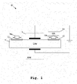
- FIG. 1 a block diagram of an exemplary embodiment of an inventive optical system 10 is shown.
- said optical system 10 comprises an optical waveguide 11, first coupling means 12 having a first focal length (f 1 ) and being optically connected to a first terminal of the optical waveguide 11, and second coupling means 13 having a second focal length (f 2 ) and being optically connected to a second terminal of the optical waveguide 11.
- the first coupling means 12 is configured to couple and/or focus incident light 16a to the optical waveguide 11.
- the second coupling means 13 is configured to emit and/or collimate light 16b conveyed by the optical waveguide 11.
- first coupling means 12 and the second coupling means 13 are confocal, wherein the second focal length (f 2 ) is smaller than the first focal length (f 1 ).
- the respective focal point is located within the optical waveguide 11.
- Such an optical system 10 can also be called confocal system.
- the optical system 10 or confocal system additionally comprises an optical sensor 14, wherein the optical sensor 14 is configured to receive the light 16b emitted and/or collimated by the second coupling means 13.
- the optical sensor 14 comprises or is a camera or an image sensor, preferably a complementary metal-oxide-semiconductor (CMOS) image sensor.
- CMOS complementary metal-oxide-semiconductor
- Such a CMOS image sensor may especially called CIS in the following.
- the first coupling means 12 may comprise at least one of a lens, preferably a Fresnel lens, a grating structure, preferably a focusing grating coupler, a diffractive element, preferably a complex diffractive component, or any combination thereof.
- the second coupling means 13 may comprise at least one of a lens, preferably a Fresnel lens, a grating structure, preferably a focusing grating coupler, a diffractive element, preferably a complex diffractive component, or any combination thereof.
- a lens preferably a Fresnel lens
- a grating structure preferably a focusing grating coupler
- a diffractive element preferably a complex diffractive component, or any combination thereof.
- the optical waveguide 11 comprises or is a slab-waveguide.
- At least one, preferably each, of the optical waveguide 11, the first coupling means 12, and the second coupling means 13 comprises at least one of liquid crystal, an electro-optic material, preferably barium titanate, geometrical variations, preferably a micro-electro-mechanical system, or any combination thereof.
- At least one, preferably each, of the optical waveguide 11, the first coupling means 12, and the second coupling means 13 may especially be configured to be thermally and/or electrically tunable.
- each of the above-mentioned liquid crystal, the electro-optic material, preferably barium titanate, the geometrical variations, preferably the micro-electro-mechanical system may exemplarily allow for said tunability.
- the confocal system 10 additionally comprises adjusting means 15, wherein the adjusting means 15 is generally configured to adjust or tune at least one optical parameter of the optical waveguide 11 and/or the first coupling means 12 and/or the second coupling means 13, preferably of the optical waveguide 11 especially at least in the region between the first coupling means 12 and the second coupling means 13.
- the adjusting means 15 adjusts or tunes the at least one optical parameter of the optical waveguide 11.
- the at least one optical parameter it is noted that it might be particularly advantageous if the at least one optical parameter comprises or is a refractive index.
- the adjusting means 15 may preferably be configured to tune an optical path distance between the first coupling means 12 and the second coupling means 13 especially in order to tune an effective magnification factor of the optical system 10.
- the adjusting means 15 may preferably be configured to bias an optical path between the first coupling means 12 and the second coupling means 13 in a biasing direction.
- the optical path and the biasing direction enclose an angle between 75 and 105 degrees, preferably between 80 and 100 degrees, more preferably between 85 and 95 degrees, most preferably 90 degrees.
- the adjusting means 15 is configured to generate an electrical field especially being parallel to the biasing direction.
- the adjusting means 15 especially is a capacitance or a capacitor, respectively, which generates said electrical field.
- the adjusting means 15 may comprise or be a modulator and/or a capacitance.
- the optical system 10 is used in the context of at least one of a mobile phone application such as a smartphone application, an imager application, a display application, an X-ray application such as application 80 according to Fig. 8 , a beyond magnification application such as application 90 according to Fig. 9 , an endoscopy application, preferably a medical endoscopy application, a time-of-flight system especially for at least one of a mobile application, an augmented reality application, an automotive and/or machine vision application, or any combination thereof.
- a mobile phone application such as a smartphone application
- an imager application such as application 80 according to Fig. 8
- a beyond magnification application such as application 90 according to Fig. 9
- an endoscopy application preferably a medical endoscopy application
- a time-of-flight system especially for at least one of a mobile application, an augmented reality application, an automotive and/or machine vision application, or any combination thereof.
- an imager application may exemplarily comprise an imager with a fixed magnification for a small CIS especially at low cost but large magnification, an imager with a zoom lens in a mobile phone especially at an ultimate small form factor, or an imager for lens-free imaging especially with large pixels.
- such a display application may exemplarily comprise an eye tracking sensor especially for an augmented reality and/or virtual reality application, preferably an augmented reality and/or virtual reality glass application.
- an eye tracking sensor especially for an augmented reality and/or virtual reality application, preferably an augmented reality and/or virtual reality glass application.
- an augmented reality and/or virtual reality application preferably an augmented reality and/or virtual reality glass application.
- an endoscopy application preferably the medical endoscopy application, it is noted that a small camera system can advantageously be integrated in disposable endoscopes.
- the intensity of a respective infrared source can advantageously be limited especially in order to fulfill eye safety requirements.
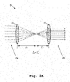
- said confocal system which specifically is a confocal magnification or demagnification, respectively, lens system, comprises a first lens 22 having a first focal length f 1 , and a second lens 23 having a second focal length f 2 .
- Said lenses 22 and 23 are arranged in free-space in a confocal manner, wherein the second focal length is smaller than the first focal length (f 2 ⁇ f 1 ).
- the two confocal lenses 22, 23 with different focal lengths as depicted in Fig. 2A form the exemplary (de)magnification system 20 especially for a free-space optics setup.
- Fig. 2B illustrates an exemplary use case 20' of the system according to Fig. 2A .
- a large window 24 to the respective scene is converted or demagnified, respectively, to a small chip imager 25 especially with dense small pixels.
- a further exemplary embodiment 30 of the inventive optical system is illustrated.
- Said exemplary embodiment 30 especially is an integrated optical magnification or demagnification, respectively, system.
- the inventive system 10 according to Fig. 1 may also be an integrated optical (or confocal) system, especially an integrated optical (de)magnification system.
- coupling structures 32, 33 such as focusing grating couplers or complex diffractive components, are used to convert three-dimensional (3D) free-space propagation to a two-dimensional (2D) free-space propagation in a slab-waveguide 31 especially with only z-direction confinement.
- first coupling structure 32 is configured to couple light into the waveguide 31, whereas the second coupling structure 33 is configured to couple light out of the waveguide 31.
- first coupling structure 32 may preferably be configured to convert 3D to 2D propagation
- second coupling structure 33 may preferably be configured to convert 2D to 3D propagation.
- the above-mentioned coupling structures 32 and 33 especially are examples for the first and second coupling means 12 and 13 according to Fig. 1
- the slab-waveguide 31 is an example of the optical waveguide 11 of Fig. 1 .
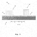
- Fig. 4 and Fig. 5 sketch the usage of the above-mentioned system 30 according to Fig. 3 for magnification ( Fig. 4 ) and demagnification ( Fig. 5 ), especially demonstrating the reciprocity of such passive confocal systems, whereas Fig. 6 being especially based on the system 30 of Fig. 3 exemplarily depicts an implementation 60 especially for increasing the effective area of a small CIS.
- the coupling structure converting 3D to 2D propagation might have to be modified especially in order to handle the proximity, and eventually bear-field mounting, of the CIS or the CIS chip, respectively.
- each component of such optical systems in the sense of the invention can be made variable by, for example, introducing liquid crystal, electro-optic materials such as barium titanate (BTO), thermal tuning, geometrical variations such as micro-electro-mechanical systems (MEMS), etc. Tuning, for instance, the optical path distance between the respective coupling structures such as the coupling structures 32 and 33, tunes the corresponding effective magnification factor.
- BTO barium titanate
- MEMS micro-electro-mechanical systems
- Said tuning of the magnification factor may be implemented in camera objectives by mechanically moving lenses or lens groups, but in accordance with the invention, this can efficiently be done especially be vertically biasing the horizontal optical path.
- this can efficiently be done especially be vertically biasing the horizontal optical path.
- only modifying one optical path may result in optical aberrations which should eventually be compensated by modifying various optical lengths and/or by tuning the focus strengths of the respective coupling structures.
- the inventive tunable (de)magnification having already been described above, which is especially obtained through optical propagation path tuning, is illustrated.
- the first coupling means of the inventive system is implemented in the form of a first varifocal lens 72 being especially embodied as a structure of the optical waveguide 71.
- the second coupling means is implemented in the form of a second varifocal lens 73 being especially embodied as a structure of the optical waveguide 71.
- the respective optical length between said lenses 72 and 73 is preferably variable.
- Said system 80 comprises a scintillator 87, an optical waveguide 81 (with coupling means) such as the waveguides 11, 31, 71 above, an optical sensor such as the optical sensor 14, exemplarily a CIS or a CIS chip 88, respectively, and a shielded box 89.
- the optical sensor can be fully protected with a shielding structure, exemplarily with the aid of the shielded box 89, which makes the design of the optical sensor or the CIS chip 88, respectively, significantly easier.
- the respective X-ray dose can be reduced while the corresponding signal-to-noise ratio is at least maintained or even increased, whereby low costs are ensured.
- the optical waveguide 81 preferably connects the scintillator 87 of the system 80 to the optical sensor or the CIS chip 88, respectively.
- Fig. 9 shows a further exemplary usage of the invention in the context of beyond magnification, which may preferably be employed for ultra compact form factor image handling such as a color direction from one RGB scene to three (or more) wavelength-dedicated imagers, or a multi-function system with 3D sent to an ID NIR imager and 2D high res sent to 2D imager, or a Fourier domain imaging in an equivalent 4F system.
- ultra compact form factor image handling such as a color direction from one RGB scene to three (or more) wavelength-dedicated imagers, or a multi-function system with 3D sent to an ID NIR imager and 2D high res sent to 2D imager, or a Fourier domain imaging in an equivalent 4F system.
- Fig. 10 shows a flow chart of an embodiment of the inventive optical method.
- incident light is coupled and/or focused to an optical waveguide with the aid of first coupling means having a first focal length and being optically connected to a first terminal of the optical waveguide.
- second step 101 light conveyed by the optical waveguide is emitted and/or collimated with the aid of second coupling means having a second focal length and being optically connected to a second terminal of the optical waveguide.
- the first coupling means and the second coupling means are confocal, wherein the second focal length is smaller than the first focal length. It is noted that such an optical method can also be called confocal method.
- the method further comprises the step of receiving the light emitted and/or collimated by the second coupling means with the aid of an optical sensor.
- the optical sensor may especially comprise or be a camera or an image sensor, preferably a complementary metal-oxide-semiconductor image sensor.
- the first coupling means may especially comprise at least one of a lens, a grating structure, preferably a focusing grating coupler, a diffractive element, preferably a complex diffractive component, or any combination thereof.
- the second coupling means may especially comprise at least one of a lens, a grating structure, preferably a focusing grating coupler, a diffractive element, preferably a complex diffractive component, or any combination thereof.
- the optical waveguide comprises or is a slab-waveguide.
- At least one, preferably each, of the optical waveguide, the first coupling means, and the second coupling means comprises at least one of liquid crystal, an electro-optic material, preferably barium titanate, geometrical variations, preferably a micro-electro-mechanical system, or any combination thereof.
- the optical method or the confocal method may further comprise the step of configuring at least one, preferably each, of the optical waveguide, the first coupling means, and the second coupling means to be thermally and/or electrically tunable.
- each of the above-mentioned liquid crystal, the electro-optic material, preferably barium titanate, the geometrical variations, preferably the micro-electro-mechanical system, may exemplarily allow for said tunability.
- the method may comprise the step of adjusting or tuning at least one optical parameter of the optical waveguide and/or the first coupling means and/or the second coupling means, preferably of the optical waveguide especially at least in the region between the first coupling means and the second coupling means, with the aid of adjusting means.
- the method may additionally or alternatively comprise the step of tuning an optical path distance between the first coupling means and the second coupling means especially in order to tune an effective magnification factor of the confocal system with the aid of the adjusting means.
- the optical method may comprise the step of biasing an optical path between the first coupling means and the second coupling means in a biasing direction with the aid of the adjusting means.
- the optical path and the biasing direction enclose an angle between 75 and 105 degrees, preferably between 80 and 100 degrees, more preferably between 85 and 95 degrees, most preferably 90 degrees.
- the optical method may additionally or alternatively comprise the step of generating an electrical field especially being parallel to the biasing direction with the aid of the adjusting means.
- the adjusting means comprises or is a modulator and/or a capacitance.
- the optical method is used in the context of at least one of an imager application, a display application, an X-ray application such as the above-mentioned application 80 according to Fig. 8 , a beyond magnification application such as the application 90 described above according to Fig. 9 , or any combination thereof.
- an imager application may exemplarily comprise an imager with a fixed magnification for a small CIS especially at low cost but large magnification, an imager with a zoom lens in a mobile phone especially at an ultimate small form factor, or an imager for lens-free imaging especially with large pixels.
- such a display application may exemplarily comprise an eye tracking sensor especially for an augmented reality and/or virtual reality application, preferably an augmented reality and/or virtual reality glass application.
Landscapes
- Physics & Mathematics (AREA)
- General Physics & Mathematics (AREA)
- Optics & Photonics (AREA)
- Health & Medical Sciences (AREA)
- Life Sciences & Earth Sciences (AREA)
- High Energy & Nuclear Physics (AREA)
- Molecular Biology (AREA)
- Spectroscopy & Molecular Physics (AREA)
- Optical Couplings Of Light Guides (AREA)
Abstract
Description
- The invention relates to an optical system, especially an integrated optical system, and a corresponding optical method.
- Generally, in times of an increasing number of applications comprising optical components such as image sensor, there is a growing need of an optical system and an optical method, which especially allow for an efficient magnification or demagnification, respectively, preferably in order to boost incoming light, and thus, in the case of such image sensors, increase image quality exemplarily due to an increased signal-to-noise ratio, which typically drops as the pixel size scales.
-
US 2020/0249491 A1 relates to a transparent wearable data display having a source of collimated light, a deflector for deflecting the collimated light into a scanned beam, and a first of switchable grating elements sandwiched between first and second parallel transparent substrates, which together function as a first light guide. A first coupling is provided for directing the scanned beam into a first total internal reflection (TIR) light path of the first light guide along the first array column. The grating elements have diffracting and non-diffracting states, in their diffracting state deflecting light out of said light guide. The grating elements are switchable into their diffracting states one group of elements at a time. Disadvantageously, in accordance with the corresponding configuration and especially due to the lack of a confocal point, said transparent wearable data display does not allow for an efficient magnification or demagnification, respectively. - Accordingly, there is an object to provide an optical system and an optical method, which ensure a magnification or a demagnification, respectively, in a significantly efficient manner.
- This object is solved by the features of
claim 1 for an optical system and the features ofclaim 15 for an optical method. The dependent claims contain further developments. - According to a first aspect of the invention, an optical system is provided. Said system comprises an optical waveguide, and at least two coupling means forming at least one confocal point being located within the optical waveguide. In this context, a first coupling means of the at least two coupling means has a first focal length. In addition to this, a second coupling means of the at least two coupling means has a second focal length. Furthermore, the first coupling means is configured to couple and/or focus incident light to the optical waveguide, whereas the second coupling means is configured to emit and/or collimate light conveyed by the optical waveguide. Advantageously, magnification or demagnification can be achieved in a particularly efficient manner. Further advantageously, with respect to the optical waveguide, a folded waveguide may be used especially in order to limit aberration.
- According to a first preferred implementation form of the first aspect of the invention, the first coupling means and the second coupling means are confocal. Additionally or alternatively, the second focal length is smaller than the first focal length. In further addition to this or as a further alternative, the optical system further comprises an optical sensor being configured to receive the light emitted and/or collimated by the second coupling means. Advantageously, light intensity at the pixel level can be increased. Further advantageously, the size of the optical sensor can be very small. As a further advantage, the size of the optical sensor is decoupled from the dimensions of the coupling means.
- According to a second preferred implementation form of the first aspect of the invention, the optical sensor comprises or is a camera or an image sensor, preferably a complementary metal-oxide-semiconductor image sensor. Advantageously, more light can be brought to the camera or the image sensor, which leads to an increased light intensity at the pixel level.
- According to a further preferred implementation form of the first aspect of the invention, the first coupling means comprises at least one of a lens, preferably a Fresnel lens, a grating structure, preferably a focusing grating coupler, a diffractive element, preferably a complex diffractive component, or any combination thereof. Additionally or alternatively, the second coupling means comprises at least one of a lens, preferably a Fresnel lens, a grating structure, preferably a focusing grating coupler, a diffractive element, preferably a complex diffractive component, or any combination thereof. In addition to this or as an alternative, if present, at least one further coupling means of the at least two coupling means comprises at least one of a lens, preferably a Fresnel lens, a grating structure, preferably a focusing grating coupler, a diffractive element, preferably a complex diffractive component, or any combination thereof. Further additionally or further alternatively, the optical waveguide comprises or is a slab-waveguide. Advantageously, at least one, preferably each, of the above-mentioned coupling means may additionally or alternatively comprise or be a fiber Bragg grating (FBG).
- According to a further preferred implementation form of the first aspect of the invention, at least one, preferably each, of the optical waveguide, the first coupling means, and the second coupling means comprises at least one of liquid crystal, an electro-optic material, preferably barium titanate, geometrical variations, preferably a micro-electro-mechanical system, or any combination thereof. Additionally, if present, at least one further coupling means of the at least two coupling means comprises at least one of liquid crystal, an electro-optic material, preferably barium titanate, geometrical variations, preferably a micro-electro-mechanical system, or any combination thereof. Advantageously, for instance, this allows for tunability or makes the respective portions of the optical system modulatable, respectively.
- According to a further preferred implementation form of the first aspect of the invention, at least one, preferably each, of the optical waveguide, the first coupling means, and the second coupling means is configured to be thermally and/or electrically tunable. In addition to this or as an alternative, if present, at least one further coupling means of the at least two coupling means is configured to be thermally and/or electrically tunable. Advantageously, each of the above-mentioned liquid crystal, the electro-optic material, preferably barium titanate, the geometrical variations, preferably the micro-electro-mechanical system, may allow for said tunability. Further advantageously, especially in the case of the above-mentioned fiber Bragg grating (FBG), it noted that tuning may be understood as modulating the corresponding positions of the reflective portions of said FBG.
- As further advantages, especially in the case that at least the optical waveguide is tunable, an optical zoom can be implemented preferably in a single-camera system exemplarily for mobile phones, no moving element is necessary for zooming, and a very compact form factor is ensured.
- Further advantageously, especially in the case that at least one, preferably the first and the second, coupling means is tunable, autofocusing and/or image stabilization can be achieved in a highly efficient manner exemplarily without any moving element.
- According to a further preferred implementation form of the first aspect of the invention, the optical system further comprises adjusting means. In this context, the adjusting means is configured to adjust or tune at least one optical parameter of the optical waveguide and/or the first coupling means and/or the second coupling means and/or, if present, at least one further coupling means of the at least two coupling means, preferably to adjust or tune at least one optical parameter of the optical waveguide especially at least in the region between the first coupling means and the second coupling means. Advantageously, for instance, tuning or modulating, respectively, can be performed in a particularly accurate and efficient manner.
- According to a further preferred implementation form of the first aspect of the invention, the at least one optical parameter comprises or is a refractive index.
- Advantageously, for example, complexity can be reduced, which leads to an increased efficiency.
- According to a further preferred implementation form of the first aspect of the invention, with respect to the optical waveguide, the adjusting means is configured to tune an optical path distance between the first coupling means and the second coupling means especially in order to tune an effective magnification factor of the optical system. Advantageously, for instance, inefficiencies can be decreased by further reducing complexity.
- According to a further preferred implementation form of the first aspect of the invention, with respect to the optical waveguide, the adjusting means is configured to bias an optical path between the first coupling means and the second coupling means in a biasing direction. Advantageously, for example, efficiency can further be increased.
- According to a further preferred implementation form of the first aspect of the invention, the optical path and the biasing direction enclose an angle between 75 and 105 degrees, preferably between 80 and 100 degrees, more preferably between 85 and 95 degrees, most preferably 90 degrees. Advantageously, for instance, not only accuracy but also efficiency can further be increased.
- According to a further preferred implementation form of the first aspect of the invention, for biasing the optical path between the first coupling means and the second coupling means, the adjusting means is configured to generate an electrical field especially being parallel to the biasing direction. Advantageously, for example, inefficiencies can further be reduced.
- According to a further preferred implementation form of the first aspect of the invention, the adjusting means comprises or is a modulator and/or a capacitance. Advantageously, for instance, complexity, and thus costs, can further be reduced, which leads to an increased efficiency.
- According to a further preferred implementation form of the first aspect of the invention, the optical system is used in the context of at least one of an imager application, a display application, an X-ray application, a beyond magnification application, an endoscopy application, preferably a medical endoscopy application, or any combination thereof. Advantageously, for example, a high flexibility can be ensured.
- Before the second aspect of the invention and its preferred implementation forms are described in the following, it is noted that all the advantages mentioned above analogously apply for the inventive optical method explained below.
- According to a second aspect of the invention, an optical method is provided. Said method comprises the steps of providing an optical waveguide and at least two coupling means, forming at least one confocal point being located within the optical waveguide with the aid of the at least two coupling means, coupling and/or focusing incident light to the optical waveguide with the aid of a first coupling means, having a first focal length, of the at least two coupling means, and emitting and/or collimating light conveyed by the optical waveguide with the aid of a second coupling means, having a second focal length, of the at least two coupling means.
- According to a first preferred implementation form of the second aspect of the invention, the first coupling means and the second coupling means are confocal. Additionally or alternatively, the second focal length is smaller than the first focal length. In further addition to this or as a further alternative, the optical method further comprises the step of receiving the light emitted and/or collimated by the second coupling means with the aid of an optical sensor.
- According to a second preferred implementation form of the second aspect of the invention, the optical sensor comprises or is a camera or an image sensor, preferably a complementary metal-oxide-semiconductor image sensor.
- According to a further preferred implementation form of the second aspect of the invention, the first coupling means comprises at least one of a lens, preferably a Fresnel lens, a grating structure, preferably a focusing grating coupler, a diffractive element, preferably a complex diffractive component, or any combination thereof. Additionally or alternatively, the second coupling means comprises at least one of a lens, preferably a Fresnel lens, a grating structure, preferably a focusing grating coupler, a diffractive element, preferably a complex diffractive component, or any combination thereof. In addition to this or as an alternative, if present, at least one further coupling means of the at least two coupling means comprises at least one of a lens, preferably a Fresnel lens, a grating structure, preferably a focusing grating coupler, a diffractive element, preferably a complex diffractive component, or any combination thereof. Further additionally or further alternatively, the optical waveguide comprises or is a slab-waveguide.
- According to a further preferred implementation form of the second aspect of the invention, at least one, preferably each, of the optical waveguide, the first coupling means, and the second coupling means comprises at least one of liquid crystal, an electro-optic material, preferably barium titanate, geometrical variations, preferably a micro-electro-mechanical system, or any combination thereof. Additionally, if present, at least one further coupling means of the at least two coupling means comprises at least one of liquid crystal, an electro-optic material, preferably barium titanate, geometrical variations, preferably a micro-electro-mechanical system, or any combination thereof.
- According to a further preferred implementation form of the second aspect of the invention, the method comprises the step of configuring at least one, preferably each, of the optical waveguide, the first coupling means, and the second coupling means to be thermally and/or electrically tunable. In addition to this or as an alternative, the optical method comprises the step of configuring, if present, at least one further coupling means of the at least two coupling means to be thermally and/or electrically tunable.
- According to a further preferred implementation form of the second aspect of the invention, the optical method further comprises the step of with the aid of adjusting means, adjusting or tuning at least one optical parameter of the optical waveguide and/or the first coupling means and/or the second coupling means and/or, if present, at least one further coupling means of the at least two coupling means, preferably adjusting or tuning at least one optical parameter of the optical waveguide especially at least in the region between the first coupling means and the second coupling means.
- According to a further preferred implementation form of the second aspect of the invention, the at least one optical parameter comprises or is a refractive index.
- According to a further preferred implementation form of the second aspect of the invention, with respect to the optical waveguide, with the aid of the adjusting means, the method comprises the step of tuning an optical path distance between the first coupling means and the second coupling means especially in order to tune a respective effective magnification factor.
- According to a further preferred implementation form of the second aspect of the invention, with respect to the optical waveguide, with the aid of the adjusting means, the optical method further comprises the step of biasing an optical path between the first coupling means and the second coupling means in a biasing direction.
- According to a further preferred implementation form of the second aspect of the invention, the optical path and the biasing direction enclose an angle between 75 and 105 degrees, preferably between 80 and 100 degrees, more preferably between 85 and 95 degrees, most preferably 90 degrees.
- According to a further preferred implementation form of the second aspect of the invention, for biasing the optical path between the first coupling means and the second coupling means, with the aid of the adjusting means, the method comprises the step of generating an electrical field especially being parallel to the biasing direction.
- According to a further preferred implementation form of the second aspect of the invention, the adjusting means comprises or is a modulator and/or a capacitance.
- According to a further preferred implementation form of the second aspect of the invention, the optical method is used in the context of at least one of an imager application, a display application, an X-ray application, a beyond magnification application, an endoscopy application, preferably a medical endoscopy application, or any combination thereof.
- Exemplary embodiments of the invention are now further explained with respect to the drawings by way of example only, and not for limitation. In the drawings:
- Fig. 1
- shows an exemplary embodiment of an inventive optical system;
- Fig. 2A
- shows an exemplary optical system in the sense of a free-space optics setup for further explanation of the invention;
- Fig. 2B
- illustrates an exemplary use case of the exemplary optical system of
Fig. 2A ; - Fig. 3
- shows an exemplary integrated confocal magnification system in the sense of the invention;
- Fig. 4
- illustrates magnification in accordance with the invention;
- Fig. 5
- illustrates demagnification according to the invention;
- Fig. 6
- shows an exemplary integrated CMOS image sensor (CIS) on flat magnification optics in the sense of the invention;
- Fig. 7
- illustrates tunable magnification obtained through optical propagation path tuning in accordance with the invention;
- Fig. 8
- shows an exemplary usage of the invention in the context of an X-ray image sensor;
- Fig. 9
- shows a further exemplary usage of the invention in the context of beyond magnification; and
- Fig. 10
- shows a flow chart of an exemplary embodiment of the inventive optical method.
- Firstly, before exemplary embodiments of the invention will be discussed in greater detail, some general and introductive aspects, especially in the form of advantages, are explained in the following.
- For instance, to overcome limitations with scaled pixel size, the invention can be used for separating focal plane to pixel array. In this context, focal plane especially means where incoming light is focused exemplarily using a lens, and pixel array especially means where incoming light is converted to electron.
- Then, the light signals illuminated on focal plane are delivered to the pixel array (for example, image sensor) using wave guide. During this delivery, the size of the image can be scaled. For example, in case of scaling down, disadvantages of the small size pixel can be overcome. Also, by changing the degree of the scaling, zooming operation can also be included.
- Generally, separating the focal plane from the imaging plane in the sense of the invention enables several advantages such as sensitivity boosting, zoom operation especially in horizontal domain (low lens module thickness), color (light wavelength) separation, and enhancing signal-to-noise ratio and/or resolution. In addition to this, especially by changing properties of the materials in between focal plane and imaging plane, optical zoom is possible. For instance, in this way, compactness of a corresponding camera hardware can be achieved.
- Now, with respect to
Fig. 1 , a block diagram of an exemplary embodiment of an inventiveoptical system 10 is shown. According toFig. 1 , saidoptical system 10 comprises anoptical waveguide 11, first coupling means 12 having a first focal length (f1) and being optically connected to a first terminal of theoptical waveguide 11, and second coupling means 13 having a second focal length (f2) and being optically connected to a second terminal of theoptical waveguide 11. - In this context, the first coupling means 12 is configured to couple and/or focus incident light 16a to the
optical waveguide 11. In addition to this, the second coupling means 13 is configured to emit and/or collimate light 16b conveyed by theoptical waveguide 11. - It is noted that with respect to the above-mentioned
incident light 16a and the above-mentioned conveyed light 16b, said kinds of light are analogously marked with the aid of the same reference signs in the context ofFig. 2A ,2B ,4 ,5 , and6 . - It is further noted that the first coupling means 12 and the second coupling means 13 are confocal, wherein the second focal length (f2) is smaller than the first focal length (f1). In this context, it should be mentioned that the respective focal point is located within the
optical waveguide 11. Such anoptical system 10 can also be called confocal system. - As it can further be seen from
Fig. 1 , theoptical system 10 or confocal system, respectively, additionally comprises anoptical sensor 14, wherein theoptical sensor 14 is configured to receive the light 16b emitted and/or collimated by the second coupling means 13. - In this context, it is noted that it might be particularly advantageous if the
optical sensor 14 comprises or is a camera or an image sensor, preferably a complementary metal-oxide-semiconductor (CMOS) image sensor. Such a CMOS image sensor may especially called CIS in the following. - With respect to the first coupling means 12, it is noted that the first coupling means 12 may comprise at least one of a lens, preferably a Fresnel lens, a grating structure, preferably a focusing grating coupler, a diffractive element, preferably a complex diffractive component, or any combination thereof.
- Additionally or alternatively, the second coupling means 13 may comprise at least one of a lens, preferably a Fresnel lens, a grating structure, preferably a focusing grating coupler, a diffractive element, preferably a complex diffractive component, or any combination thereof. With respect to the
optical waveguide 11, it is noted that it might be particularly advantageous if theoptical waveguide 11 comprises or is a slab-waveguide. - Furthermore, it might be also particularly advantageous if at least one, preferably each, of the
optical waveguide 11, the first coupling means 12, and the second coupling means 13 comprises at least one of liquid crystal, an electro-optic material, preferably barium titanate, geometrical variations, preferably a micro-electro-mechanical system, or any combination thereof. - Moreover, at least one, preferably each, of the
optical waveguide 11, the first coupling means 12, and the second coupling means 13 may especially be configured to be thermally and/or electrically tunable. In this context, it is noted that each of the above-mentioned liquid crystal, the electro-optic material, preferably barium titanate, the geometrical variations, preferably the micro-electro-mechanical system, may exemplarily allow for said tunability. - In further accordance with
Fig. 1 , theconfocal system 10 additionally comprises adjusting means 15, wherein the adjusting means 15 is generally configured to adjust or tune at least one optical parameter of theoptical waveguide 11 and/or the first coupling means 12 and/or the second coupling means 13, preferably of theoptical waveguide 11 especially at least in the region between the first coupling means 12 and the second coupling means 13. - In this exemplary embodiment, said preferred alternative is implemented. Accordingly, the adjusting means 15 adjusts or tunes the at least one optical parameter of the
optical waveguide 11. With respect to the at least one optical parameter, it is noted that it might be particularly advantageous if the at least one optical parameter comprises or is a refractive index. - In addition to this or as an alternative, with respect to the
optical waveguide 11, the adjusting means 15 may preferably be configured to tune an optical path distance between the first coupling means 12 and the second coupling means 13 especially in order to tune an effective magnification factor of theoptical system 10. - Further additionally or further alternatively, also with respect to the
optical waveguide 11, the adjusting means 15 may preferably be configured to bias an optical path between the first coupling means 12 and the second coupling means 13 in a biasing direction. In this context, it might be particularly advantageous if the optical path and the biasing direction enclose an angle between 75 and 105 degrees, preferably between 80 and 100 degrees, more preferably between 85 and 95 degrees, most preferably 90 degrees. - Furthermore, for biasing the optical path between the first coupling means 12 and the second coupling means 13, the adjusting means 15 is configured to generate an electrical field especially being parallel to the biasing direction. Exemplarily, as it can be seen from
Fig. 1 , the adjusting means 15 especially is a capacitance or a capacitor, respectively, which generates said electrical field. As an alternative, it is noted that the adjusting means 15 may comprise or be a modulator and/or a capacitance. - Fundamentally, it is noted that it might be particularly advantageous if the
optical system 10 is used in the context of at least one of a mobile phone application such as a smartphone application, an imager application, a display application, an X-ray application such asapplication 80 according toFig. 8 , a beyond magnification application such asapplication 90 according toFig. 9 , an endoscopy application, preferably a medical endoscopy application, a time-of-flight system especially for at least one of a mobile application, an augmented reality application, an automotive and/or machine vision application, or any combination thereof. - With respect to the above-mentioned imager application, it is noted that such an imager application may exemplarily comprise an imager with a fixed magnification for a small CIS especially at low cost but large magnification, an imager with a zoom lens in a mobile phone especially at an ultimate small form factor, or an imager for lens-free imaging especially with large pixels.
- Furthermore, with respect to the above-mentioned display application, such a display application may exemplarily comprise an eye tracking sensor especially for an augmented reality and/or virtual reality application, preferably an augmented reality and/or virtual reality glass application. Moreover, with respect to the above-mentioned endoscopy application, preferably the medical endoscopy application, it is noted that a small camera system can advantageously be integrated in disposable endoscopes.
- In addition to this, regarding the eye tracking sensor mentioned above and/or with respect to the above-mentioned time-of-flight system especially for at least one of a mobile application, an augmented reality application, an automotive and/or machine vision application, it is noted that the intensity of a respective infrared source can advantageously be limited especially in order to fulfill eye safety requirements.
- Now, on the basis of
Fig. 2A andFig. 2B showing an exemplaryconfocal system 20 in the sense of a free-space optics setup, the invention is further explained in the following. - As it can be seen from
Fig. 2A , said confocal system, which specifically is a confocal magnification or demagnification, respectively, lens system, comprises afirst lens 22 having a first focal length f1, and asecond lens 23 having a second focal length f2. Saidlenses confocal lenses Fig. 2A form the exemplary (de)magnification system 20 especially for a free-space optics setup. - In this context,
Fig. 2B illustrates an exemplary use case 20' of the system according toFig. 2A . As it can be seen, alarge window 24 to the respective scene is converted or demagnified, respectively, to asmall chip imager 25 especially with dense small pixels. - Furthermore, with respect to
Fig. 3 , a furtherexemplary embodiment 30 of the inventive optical system is illustrated. Saidexemplary embodiment 30 especially is an integrated optical magnification or demagnification, respectively, system. In this context, it is noted that theinventive system 10 according toFig. 1 may also be an integrated optical (or confocal) system, especially an integrated optical (de)magnification system. - In this exemplary case according to
Fig. 3 ,coupling structures waveguide 31 especially with only z-direction confinement. - It might be particularly advantageous if the
first coupling structure 32 is configured to couple light into thewaveguide 31, whereas thesecond coupling structure 33 is configured to couple light out of thewaveguide 31. In this context, thefirst coupling structure 32 may preferably be configured to convert 3D to 2D propagation, whereas thesecond coupling structure 33 may preferably be configured to convert 2D to 3D propagation. It is noted that the above-mentionedcoupling structures Fig. 1 , whereas the slab-waveguide 31 is an example of theoptical waveguide 11 ofFig. 1 . - Moreover,
Fig. 4 andFig. 5 sketch the usage of the above-mentionedsystem 30 according toFig. 3 for magnification (Fig. 4 ) and demagnification (Fig. 5 ), especially demonstrating the reciprocity of such passive confocal systems, whereasFig. 6 being especially based on thesystem 30 ofFig. 3 exemplarily depicts animplementation 60 especially for increasing the effective area of a small CIS. - In the context of
Fig. 6 , it is noted that the coupling structure converting 3D to 2D propagation might have to be modified especially in order to handle the proximity, and eventually bear-field mounting, of the CIS or the CIS chip, respectively. - It is further noted that each component of such optical systems in the sense of the invention can be made variable by, for example, introducing liquid crystal, electro-optic materials such as barium titanate (BTO), thermal tuning, geometrical variations such as micro-electro-mechanical systems (MEMS), etc. Tuning, for instance, the optical path distance between the respective coupling structures such as the
coupling structures - Said tuning of the magnification factor may be implemented in camera objectives by mechanically moving lenses or lens groups, but in accordance with the invention, this can efficiently be done especially be vertically biasing the horizontal optical path. In this context, it is noted that only modifying one optical path may result in optical aberrations which should eventually be compensated by modifying various optical lengths and/or by tuning the focus strengths of the respective coupling structures.
- Again, with respect to
Fig. 6 , it is noted that for the implementation case of increasing the effective area of the CIS, pixel with super high full well capacity might be essential, while especially keeping the noise level low preferably to cope with increased illumination level. It is further noted that the foregoing explanations, especially regarding image sensor systems, can analogously be applied to projection systems and to alternative applications, wherein fixed or tunable magnifications are required. - With respect to
Fig. 7 , the inventive tunable (de)magnification having already been described above, which is especially obtained through optical propagation path tuning, is illustrated. As it can be seen fromFig. 7 , the first coupling means of the inventive system is implemented in the form of a firstvarifocal lens 72 being especially embodied as a structure of theoptical waveguide 71. Furthermore, the second coupling means is implemented in the form of a secondvarifocal lens 73 being especially embodied as a structure of theoptical waveguide 71. Moreover, the respective optical length between saidlenses - Now, with respect to
Fig. 8 , an exemplary usage, especially in the form of asystem 80, of the invention in the context of an X-ray image sensor is depicted. Saidsystem 80 comprises ascintillator 87, an optical waveguide 81 (with coupling means) such as thewaveguides optical sensor 14, exemplarily a CIS or aCIS chip 88, respectively, and a shieldedbox 89. - It is particularly advantageous that the optical sensor can be fully protected with a shielding structure, exemplarily with the aid of the shielded
box 89, which makes the design of the optical sensor or theCIS chip 88, respectively, significantly easier. - Further advantageously, the respective X-ray dose can be reduced while the corresponding signal-to-noise ratio is at least maintained or even increased, whereby low costs are ensured. In this context, the
optical waveguide 81 preferably connects thescintillator 87 of thesystem 80 to the optical sensor or theCIS chip 88, respectively. -
Fig. 9 shows a further exemplary usage of the invention in the context of beyond magnification, which may preferably be employed for ultra compact form factor image handling such as a color direction from one RGB scene to three (or more) wavelength-dedicated imagers, or a multi-function system with 3D sent to an ID NIR imager and 2D high res sent to 2D imager, or a Fourier domain imaging in an equivalent 4F system. - Finally,
Fig. 10 shows a flow chart of an embodiment of the inventive optical method. In afirst step 100, incident light is coupled and/or focused to an optical waveguide with the aid of first coupling means having a first focal length and being optically connected to a first terminal of the optical waveguide. Then, in asecond step 101, light conveyed by the optical waveguide is emitted and/or collimated with the aid of second coupling means having a second focal length and being optically connected to a second terminal of the optical waveguide. In this context, the first coupling means and the second coupling means are confocal, wherein the second focal length is smaller than the first focal length. It is noted that such an optical method can also be called confocal method. - It might be particularly advantageous if the method further comprises the step of receiving the light emitted and/or collimated by the second coupling means with the aid of an optical sensor. In this context, the optical sensor may especially comprise or be a camera or an image sensor, preferably a complementary metal-oxide-semiconductor image sensor.
- With respect to the first coupling means, it is noted that the first coupling means may especially comprise at least one of a lens, a grating structure, preferably a focusing grating coupler, a diffractive element, preferably a complex diffractive component, or any combination thereof.
- Additionally or alternatively, the second coupling means may especially comprise at least one of a lens, a grating structure, preferably a focusing grating coupler, a diffractive element, preferably a complex diffractive component, or any combination thereof.
- With respect to the optical waveguide, it is noted that it might be particularly advantageous if the optical waveguide comprises or is a slab-waveguide.
- It is further noted that it might be also particularly advantageous if at least one, preferably each, of the optical waveguide, the first coupling means, and the second coupling means comprises at least one of liquid crystal, an electro-optic material, preferably barium titanate, geometrical variations, preferably a micro-electro-mechanical system, or any combination thereof.
- Moreover, the optical method or the confocal method, respectively, may further comprise the step of configuring at least one, preferably each, of the optical waveguide, the first coupling means, and the second coupling means to be thermally and/or electrically tunable.
- In this context, it is noted that each of the above-mentioned liquid crystal, the electro-optic material, preferably barium titanate, the geometrical variations, preferably the micro-electro-mechanical system, may exemplarily allow for said tunability.
- In addition to this or as an alternative, the method may comprise the step of adjusting or tuning at least one optical parameter of the optical waveguide and/or the first coupling means and/or the second coupling means, preferably of the optical waveguide especially at least in the region between the first coupling means and the second coupling means, with the aid of adjusting means.
- With respect to the above-mentioned at least one optical parameter, it might be particularly advantageous if the at least one optical parameter comprises or is a refractive index. Moreover, with respect to the optical waveguide, the method may additionally or alternatively comprise the step of tuning an optical path distance between the first coupling means and the second coupling means especially in order to tune an effective magnification factor of the confocal system with the aid of the adjusting means.
- In further addition to this or as a further alternative, with respect to the optical waveguide, the optical method may comprise the step of biasing an optical path between the first coupling means and the second coupling means in a biasing direction with the aid of the adjusting means.
- In this context, it might be particularly advantageous if the optical path and the biasing direction enclose an angle between 75 and 105 degrees, preferably between 80 and 100 degrees, more preferably between 85 and 95 degrees, most preferably 90 degrees.
- Furthermore, for biasing the optical path between the first coupling means and the second coupling means, the optical method may additionally or alternatively comprise the step of generating an electrical field especially being parallel to the biasing direction with the aid of the adjusting means.
- With respect to the adjusting means, it is noted that it might be particularly advantageous if the adjusting means comprises or is a modulator and/or a capacitance.
- Fundamentally, it is noted that it might be particularly advantageous if the optical method is used in the context of at least one of an imager application, a display application, an X-ray application such as the above-mentioned
application 80 according toFig. 8 , a beyond magnification application such as theapplication 90 described above according toFig. 9 , or any combination thereof. - With respect to the above-mentioned imager application, it is noted that such an imager application may exemplarily comprise an imager with a fixed magnification for a small CIS especially at low cost but large magnification, an imager with a zoom lens in a mobile phone especially at an ultimate small form factor, or an imager for lens-free imaging especially with large pixels.
- Furthermore, with respect to the above-mentioned display application, such a display application may exemplarily comprise an eye tracking sensor especially for an augmented reality and/or virtual reality application, preferably an augmented reality and/or virtual reality glass application.
- While various embodiments of the present invention have been described above, it should be understood that they have been presented by way of example only, and not limitation. Numerous changes to the disclosed embodiments can be made in accordance with the disclosure herein without departing from the spirit or scope of the invention. Thus, the breadth and scope of the present invention should not be limited by any of the above described embodiments. Rather, the scope of the invention should be defined in accordance with the following claims and their equivalents.
- Although the invention has been illustrated and described with respect to one or more implementations, equivalent alterations and modifications will occur to others skilled in the art upon the reading and understanding of this specification and the annexed drawings. In addition, while a particular feature of the invention may have been disclosed with respect to only one of several implementations, such feature may be combined with one or more other features of the other implementations as may be desired and advantageous for any given or particular application.
Claims (15)
- An optical system (10) comprising:an optical waveguide (11),at least a first coupling means (12) having a first focal length (f1), andat least a second coupling means (13) having a second focal length (f2),wherein the first coupling means (12) is configured to couple and/or focus incident light (16a) to the optical waveguide (11),
wherein the second coupling means (13) is configured to emit and/or collimate light (16b) conveyed by the optical waveguide (11), and
wherein the at least two coupling means (12, 13) are both focusing on at least one confocal point being located within the optical waveguide (11). - The optical system (10) according to claim 1,
wherein the first coupling means (12) and the second coupling means (13) are confocal, and/or
wherein the second focal length (f2) is smaller than the first focal length (f1), and/or
wherein the optical system (10) further comprises an optical sensor (14) being configured to receive the light (16b) emitted and/or collimated by the second coupling means (13) . - The optical system (10) according to claim 2,
wherein the optical sensor (14) comprises or is a camera or an image sensor, preferably a complementary metal-oxide-semiconductor image sensor. - The optical system (10) according to any of the claims 1 to 3,
wherein the first coupling means (12) comprises at least one of a lens, preferably a Fresnel lens, a grating structure, preferably a focusing grating coupler, a diffractive element, preferably a complex diffractive component, or any combination thereof, and/or
wherein the second coupling means (13) comprises at least one of a lens, preferably a Fresnel lens, a grating structure, preferably a focusing grating coupler, a diffractive element, preferably a complex diffractive component, or any combination thereof, and/or
wherein, if present, at least one further coupling means of the at least two coupling means (12, 13) comprises at least one of a lens, preferably a Fresnel lens, a grating structure, preferably a focusing grating coupler, a diffractive element, preferably a complex diffractive component, or any combination thereof, and/or
wherein the optical waveguide (11) comprises or is a slab-waveguide. - The optical system (10) according to any of the claims 1 to 4,
wherein at least one, preferably each, of the optical waveguide (11), the first coupling means (12), and the second coupling means (13) comprises at least one of liquid crystal, an electro-optic material, preferably barium titanate, geometrical variations, preferably a micro-electro-mechanical system, or any combination thereof, and/or
wherein, if present, at least one further coupling means of the at least two coupling means (12, 13) comprises at least one of liquid crystal, an electro-optic material, preferably barium titanate, geometrical variations, preferably a micro-electro-mechanical system, or any combination thereof. - The optical system (10) according to any of the claims 1 to 5,
wherein at least one, preferably each, of the optical waveguide (11), the first coupling means (12), and the second coupling means (13) is configured to be thermally and/or electrically tunable, and/or
wherein, if present, at least one further coupling means of the at least two coupling means (12, 13) is configured to be thermally and/or electrically tunable. - The optical system (10) according to any of the claims 1 to 6,
wherein the optical system (10) further comprises adjusting means (15),
wherein the adjusting means (15) is configured to adjust or tune at least one optical parameter of the optical waveguide (11) and/or the first coupling means (12) and/or the second coupling means (13) and/or, if present, at least one further coupling means of the at least two coupling means (12, 13), preferably to adjust or tune at least one optical parameter of the optical waveguide (11) especially at least in the region between the first coupling means (12) and the second coupling means (13). - The optical system (10) according to claim 7,
wherein the at least one optical parameter comprises or is a refractive index. - The optical system (10) according to claim 7 or 8,
wherein with respect to the optical waveguide (11), the adjusting means (15) is configured to tune an optical path distance between the first coupling means (12) and the second coupling means (13) especially in order to tune an effective magnification factor of the optical system (10). - The optical system (10) according to any of the claims 7 to 9,
wherein with respect to the optical waveguide (11), the adjusting means (15) is configured to bias an optical path between the first coupling means (12) and the second coupling means (13) in a biasing direction. - The optical system (10) according to claim 10,
wherein the optical path and the biasing direction enclose an angle between 75 and 105 degrees, preferably between 80 and 100 degrees, more preferably between 85 and 95 degrees, most preferably 90 degrees. - The optical system (10) according to claim 10 or 11,
wherein for biasing the optical path between the first coupling means (12) and the second coupling means (13), the adjusting means (15) is configured to generate an electrical field especially being parallel to the biasing direction. - The optical system (10) according to any of the claims 7 to 12,
wherein the adjusting means (15) comprises or is a modulator and/or a capacitance. - The optical system (10) according to any of the claims 1 to 13,
wherein the optical system (10) is used in the context of at least one of an imager application, a display application, an X-ray application (80), a beyond magnification application (90), an endoscopy application, preferably a medical endoscopy application, or any combination thereof. - An optical method comprising the steps of:providing an optical waveguide (11) and at least two coupling means (12, 13),coupling and/or focusing incident light (16a) to the optical waveguide (11) with the aid of a first coupling means (12), having a first focal length (f1), of the at least two coupling means (12, 13),emitting and/or collimating light (16b) conveyed by the optical waveguide (11) with the aid of a second coupling means (13), having a second focal length (f2), of the at least two coupling means (12, 13), andforming at least one confocal point being located within the optical waveguide (11) with the aid of the at least two coupling means (12, 13).
Priority Applications (2)
| Application Number | Priority Date | Filing Date | Title |
|---|---|---|---|
| EP21171427.4A EP4083680B1 (en) | 2021-04-30 | 2021-04-30 | Optical system and corresponding optical method |
| US17/661,251 US12366672B2 (en) | 2021-04-30 | 2022-04-28 | Optical system and corresponding optical method |
Applications Claiming Priority (1)
| Application Number | Priority Date | Filing Date | Title |
|---|---|---|---|
| EP21171427.4A EP4083680B1 (en) | 2021-04-30 | 2021-04-30 | Optical system and corresponding optical method |
Publications (2)
| Publication Number | Publication Date |
|---|---|
| EP4083680A1 true EP4083680A1 (en) | 2022-11-02 |
| EP4083680B1 EP4083680B1 (en) | 2025-08-13 |
Family
ID=75746390
Family Applications (1)
| Application Number | Title | Priority Date | Filing Date |
|---|---|---|---|
| EP21171427.4A Active EP4083680B1 (en) | 2021-04-30 | 2021-04-30 | Optical system and corresponding optical method |
Country Status (2)
| Country | Link |
|---|---|
| US (1) | US12366672B2 (en) |
| EP (1) | EP4083680B1 (en) |
Families Citing this family (1)
| Publication number | Priority date | Publication date | Assignee | Title |
|---|---|---|---|---|
| US12498572B2 (en) * | 2021-11-14 | 2025-12-16 | Fourier Optics Ltd | System and method for optically combining virtual images into real world scenery |
Citations (5)
| Publication number | Priority date | Publication date | Assignee | Title |
|---|---|---|---|---|
| EP0360209A2 (en) * | 1988-09-19 | 1990-03-28 | Hitachi, Ltd. | Optical head and optical data processing apparatus |
| CN106909047A (en) * | 2017-04-20 | 2017-06-30 | 北京理工大学 | Multilayer calculates holographic chromatic aberation and eliminates and diopter correction waveguide display methods and system |
| CN106526730B (en) * | 2016-11-21 | 2019-07-12 | 苏州苏大维格光电科技股份有限公司 | A kind of wide viewing angle waveguide eyeglass and production method and wear-type three-dimensional display apparatus |
| US10437064B2 (en) * | 2015-01-12 | 2019-10-08 | Digilens Inc. | Environmentally isolated waveguide display |
| US20200249491A1 (en) | 2011-08-24 | 2020-08-06 | Digilens Inc. | Wearable Data Display |
Family Cites Families (6)
| Publication number | Priority date | Publication date | Assignee | Title |
|---|---|---|---|---|
| CN113433700B (en) | 2013-11-27 | 2024-03-22 | 奇跃公司 | Virtual and augmented reality systems and methods |
| US9885657B2 (en) | 2014-08-08 | 2018-02-06 | Quantum-Si Incorporated | Integrated device with external light source for probing detecting and analyzing molecules |
| US10560689B2 (en) | 2017-11-28 | 2020-02-11 | Paul Lapstun | Viewpoint-optimized light field display |
| US11822079B2 (en) * | 2018-08-10 | 2023-11-21 | Apple Inc. | Waveguided display system with adjustable lenses |
| US20200225471A1 (en) | 2019-01-14 | 2020-07-16 | Digilens Inc. | Holographic Waveguide Display with Light Control Layer |
| DE102019102607A1 (en) * | 2019-02-01 | 2020-08-06 | Carl Zeiss Jena Gmbh | Functionalized waveguide for a detector system |
-
2021
- 2021-04-30 EP EP21171427.4A patent/EP4083680B1/en active Active
-
2022
- 2022-04-28 US US17/661,251 patent/US12366672B2/en active Active
Patent Citations (5)
| Publication number | Priority date | Publication date | Assignee | Title |
|---|---|---|---|---|
| EP0360209A2 (en) * | 1988-09-19 | 1990-03-28 | Hitachi, Ltd. | Optical head and optical data processing apparatus |
| US20200249491A1 (en) | 2011-08-24 | 2020-08-06 | Digilens Inc. | Wearable Data Display |
| US10437064B2 (en) * | 2015-01-12 | 2019-10-08 | Digilens Inc. | Environmentally isolated waveguide display |
| CN106526730B (en) * | 2016-11-21 | 2019-07-12 | 苏州苏大维格光电科技股份有限公司 | A kind of wide viewing angle waveguide eyeglass and production method and wear-type three-dimensional display apparatus |
| CN106909047A (en) * | 2017-04-20 | 2017-06-30 | 北京理工大学 | Multilayer calculates holographic chromatic aberation and eliminates and diopter correction waveguide display methods and system |
Also Published As
| Publication number | Publication date |
|---|---|
| EP4083680B1 (en) | 2025-08-13 |
| US20220350040A1 (en) | 2022-11-03 |
| US12366672B2 (en) | 2025-07-22 |
Similar Documents
| Publication | Publication Date | Title |
|---|---|---|
| US10359608B2 (en) | Bifocal lens and imaging device including same | |
| CN1042386C (en) | Video projection system | |
| JP5910739B2 (en) | Imaging device | |
| CN109194859B (en) | Camera and terminal equipment | |
| EP2369401B1 (en) | Optical modulator device and spatio-temporally light modulated imaging system | |
| CN111866328B (en) | A camera module and mobile terminal | |
| JP2007528020A (en) | Projection device | |
| US10890743B2 (en) | Illumination device and microscope device | |
| US20190384049A1 (en) | Image conversion module for a microscope and microscope | |
| JP2020523625A (en) | Multi-aperture imaging device, imaging system, and method for providing a multi-aperture imaging device | |
| JP7783949B2 (en) | Time-of-flight camera | |
| US20180164562A1 (en) | Confocal microscopy system with vari-focus optical element | |
| US12174120B2 (en) | Image acquisition device, image acquisition method, and spatial light modulation unit | |
| US12366672B2 (en) | Optical system and corresponding optical method | |
| CN113302535B (en) | Filming equipment | |
| JP2012133026A (en) | Focal length variable prism and prism optical system using the same | |
| CN113485005A (en) | Modular zoom lens with high optical expansion for machine vision | |
| CN113302534B (en) | Optical system, optical device and photographing device | |
| US20230408727A1 (en) | Folded optical paths incorporating metasurfaces | |
| CN113302536B (en) | Image capturing apparatus | |
| KR20100096398A (en) | Illumination apparatus | |
| KR20100048092A (en) | Zoom expander | |
| KR100531383B1 (en) | zoom lens of ultra wide angle in projection system | |
| CN113031132B (en) | Adapter optical system and focus-variable optical system | |
| KR20230108208A (en) | Camera with tiltable optical field of view changing elements |
Legal Events
| Date | Code | Title | Description |
|---|---|---|---|
| PUAI | Public reference made under article 153(3) epc to a published international application that has entered the european phase |
Free format text: ORIGINAL CODE: 0009012 |
|
| STAA | Information on the status of an ep patent application or granted ep patent |
Free format text: STATUS: THE APPLICATION HAS BEEN PUBLISHED |
|
| AK | Designated contracting states |
Kind code of ref document: A1 Designated state(s): AL AT BE BG CH CY CZ DE DK EE ES FI FR GB GR HR HU IE IS IT LI LT LU LV MC MK MT NL NO PL PT RO RS SE SI SK SM TR |
|
| STAA | Information on the status of an ep patent application or granted ep patent |
Free format text: STATUS: REQUEST FOR EXAMINATION WAS MADE |
|
| 17P | Request for examination filed |
Effective date: 20230502 |
|
| RBV | Designated contracting states (corrected) |
Designated state(s): AL AT BE BG CH CY CZ DE DK EE ES FI FR GB GR HR HU IE IS IT LI LT LU LV MC MK MT NL NO PL PT RO RS SE SI SK SM TR |
|
| GRAP | Despatch of communication of intention to grant a patent |
Free format text: ORIGINAL CODE: EPIDOSNIGR1 |
|
| STAA | Information on the status of an ep patent application or granted ep patent |
Free format text: STATUS: GRANT OF PATENT IS INTENDED |
|
| RIC1 | Information provided on ipc code assigned before grant |
Ipc: G02B 27/42 20060101ALN20241111BHEP Ipc: G02B 6/34 20060101ALI20241111BHEP Ipc: G02B 27/01 20060101AFI20241111BHEP |
|
| INTG | Intention to grant announced |
Effective date: 20241203 |
|
| RIC1 | Information provided on ipc code assigned before grant |
Ipc: G02B 27/42 20060101ALN20241122BHEP Ipc: G02B 6/34 20060101ALI20241122BHEP Ipc: G02B 27/01 20060101AFI20241122BHEP |
|
| GRAJ | Information related to disapproval of communication of intention to grant by the applicant or resumption of examination proceedings by the epo deleted |
Free format text: ORIGINAL CODE: EPIDOSDIGR1 |
|
| STAA | Information on the status of an ep patent application or granted ep patent |
Free format text: STATUS: REQUEST FOR EXAMINATION WAS MADE |
|
| GRAP | Despatch of communication of intention to grant a patent |
Free format text: ORIGINAL CODE: EPIDOSNIGR1 |
|
| STAA | Information on the status of an ep patent application or granted ep patent |
Free format text: STATUS: GRANT OF PATENT IS INTENDED |
|
| INTC | Intention to grant announced (deleted) | ||
| RIC1 | Information provided on ipc code assigned before grant |
Ipc: G02B 27/42 20060101ALN20250320BHEP Ipc: G02B 6/34 20060101ALI20250320BHEP Ipc: G02B 27/01 20060101AFI20250320BHEP |
|
| INTG | Intention to grant announced |
Effective date: 20250401 |
|
| P01 | Opt-out of the competence of the unified patent court (upc) registered |
Free format text: CASE NUMBER: APP_14889/2025 Effective date: 20250327 |
|
| GRAS | Grant fee paid |
Free format text: ORIGINAL CODE: EPIDOSNIGR3 |
|
| GRAA | (expected) grant |
Free format text: ORIGINAL CODE: 0009210 |
|
| STAA | Information on the status of an ep patent application or granted ep patent |
Free format text: STATUS: THE PATENT HAS BEEN GRANTED |
|
| AK | Designated contracting states |
Kind code of ref document: B1 Designated state(s): AL AT BE BG CH CY CZ DE DK EE ES FI FR GB GR HR HU IE IS IT LI LT LU LV MC MK MT NL NO PL PT RO RS SE SI SK SM TR |
|
| REG | Reference to a national code |
Ref country code: GB Ref legal event code: FG4D |
|
| REG | Reference to a national code |
Ref country code: CH Ref legal event code: EP |
|
| REG | Reference to a national code |
Ref country code: DE Ref legal event code: R096 Ref document number: 602021035954 Country of ref document: DE |
|
| REG | Reference to a national code |
Ref country code: IE Ref legal event code: FG4D |
|
| REG | Reference to a national code |
Ref country code: NL Ref legal event code: MP Effective date: 20250813 |
|
| PG25 | Lapsed in a contracting state [announced via postgrant information from national office to epo] |
Ref country code: IS Free format text: LAPSE BECAUSE OF FAILURE TO SUBMIT A TRANSLATION OF THE DESCRIPTION OR TO PAY THE FEE WITHIN THE PRESCRIBED TIME-LIMIT Effective date: 20251213 |
|
| PG25 | Lapsed in a contracting state [announced via postgrant information from national office to epo] |
Ref country code: NO Free format text: LAPSE BECAUSE OF FAILURE TO SUBMIT A TRANSLATION OF THE DESCRIPTION OR TO PAY THE FEE WITHIN THE PRESCRIBED TIME-LIMIT Effective date: 20251113 |
|
| REG | Reference to a national code |
Ref country code: LT Ref legal event code: MG9D |
|
| PG25 | Lapsed in a contracting state [announced via postgrant information from national office to epo] |
Ref country code: PT Free format text: LAPSE BECAUSE OF FAILURE TO SUBMIT A TRANSLATION OF THE DESCRIPTION OR TO PAY THE FEE WITHIN THE PRESCRIBED TIME-LIMIT Effective date: 20251215 |
|
| PG25 | Lapsed in a contracting state [announced via postgrant information from national office to epo] |
Ref country code: FI Free format text: LAPSE BECAUSE OF FAILURE TO SUBMIT A TRANSLATION OF THE DESCRIPTION OR TO PAY THE FEE WITHIN THE PRESCRIBED TIME-LIMIT Effective date: 20250813 |
|
| PG25 | Lapsed in a contracting state [announced via postgrant information from national office to epo] |
Ref country code: HR Free format text: LAPSE BECAUSE OF FAILURE TO SUBMIT A TRANSLATION OF THE DESCRIPTION OR TO PAY THE FEE WITHIN THE PRESCRIBED TIME-LIMIT Effective date: 20250813 Ref country code: NL Free format text: LAPSE BECAUSE OF FAILURE TO SUBMIT A TRANSLATION OF THE DESCRIPTION OR TO PAY THE FEE WITHIN THE PRESCRIBED TIME-LIMIT Effective date: 20250813 |
|
| PG25 | Lapsed in a contracting state [announced via postgrant information from national office to epo] |
Ref country code: GR Free format text: LAPSE BECAUSE OF FAILURE TO SUBMIT A TRANSLATION OF THE DESCRIPTION OR TO PAY THE FEE WITHIN THE PRESCRIBED TIME-LIMIT Effective date: 20251114 |
|
| PG25 | Lapsed in a contracting state [announced via postgrant information from national office to epo] |
Ref country code: SE Free format text: LAPSE BECAUSE OF FAILURE TO SUBMIT A TRANSLATION OF THE DESCRIPTION OR TO PAY THE FEE WITHIN THE PRESCRIBED TIME-LIMIT Effective date: 20250813 |
|
| PG25 | Lapsed in a contracting state [announced via postgrant information from national office to epo] |
Ref country code: LV Free format text: LAPSE BECAUSE OF FAILURE TO SUBMIT A TRANSLATION OF THE DESCRIPTION OR TO PAY THE FEE WITHIN THE PRESCRIBED TIME-LIMIT Effective date: 20250813 |
|
| PG25 | Lapsed in a contracting state [announced via postgrant information from national office to epo] |
Ref country code: BG Free format text: LAPSE BECAUSE OF FAILURE TO SUBMIT A TRANSLATION OF THE DESCRIPTION OR TO PAY THE FEE WITHIN THE PRESCRIBED TIME-LIMIT Effective date: 20250813 Ref country code: PL Free format text: LAPSE BECAUSE OF FAILURE TO SUBMIT A TRANSLATION OF THE DESCRIPTION OR TO PAY THE FEE WITHIN THE PRESCRIBED TIME-LIMIT Effective date: 20250813 |
|
| PG25 | Lapsed in a contracting state [announced via postgrant information from national office to epo] |
Ref country code: RS Free format text: LAPSE BECAUSE OF FAILURE TO SUBMIT A TRANSLATION OF THE DESCRIPTION OR TO PAY THE FEE WITHIN THE PRESCRIBED TIME-LIMIT Effective date: 20251113 |
|
| PG25 | Lapsed in a contracting state [announced via postgrant information from national office to epo] |
Ref country code: ES Free format text: LAPSE BECAUSE OF FAILURE TO SUBMIT A TRANSLATION OF THE DESCRIPTION OR TO PAY THE FEE WITHIN THE PRESCRIBED TIME-LIMIT Effective date: 20250813 |
|
| REG | Reference to a national code |
Ref country code: AT Ref legal event code: MK05 Ref document number: 1825296 Country of ref document: AT Kind code of ref document: T Effective date: 20250813 |
|
| PG25 | Lapsed in a contracting state [announced via postgrant information from national office to epo] |
Ref country code: SM Free format text: LAPSE BECAUSE OF FAILURE TO SUBMIT A TRANSLATION OF THE DESCRIPTION OR TO PAY THE FEE WITHIN THE PRESCRIBED TIME-LIMIT Effective date: 20250813 |
|
| PG25 | Lapsed in a contracting state [announced via postgrant information from national office to epo] |
Ref country code: DK Free format text: LAPSE BECAUSE OF FAILURE TO SUBMIT A TRANSLATION OF THE DESCRIPTION OR TO PAY THE FEE WITHIN THE PRESCRIBED TIME-LIMIT Effective date: 20250813 |
|
| PG25 | Lapsed in a contracting state [announced via postgrant information from national office to epo] |
Ref country code: AT Free format text: LAPSE BECAUSE OF FAILURE TO SUBMIT A TRANSLATION OF THE DESCRIPTION OR TO PAY THE FEE WITHIN THE PRESCRIBED TIME-LIMIT Effective date: 20250813 |
|
| PG25 | Lapsed in a contracting state [announced via postgrant information from national office to epo] |
Ref country code: IT Free format text: LAPSE BECAUSE OF FAILURE TO SUBMIT A TRANSLATION OF THE DESCRIPTION OR TO PAY THE FEE WITHIN THE PRESCRIBED TIME-LIMIT Effective date: 20250813 |
|
| PG25 | Lapsed in a contracting state [announced via postgrant information from national office to epo] |
Ref country code: CZ Free format text: LAPSE BECAUSE OF FAILURE TO SUBMIT A TRANSLATION OF THE DESCRIPTION OR TO PAY THE FEE WITHIN THE PRESCRIBED TIME-LIMIT Effective date: 20250813 |
|
| PG25 | Lapsed in a contracting state [announced via postgrant information from national office to epo] |
Ref country code: EE Free format text: LAPSE BECAUSE OF FAILURE TO SUBMIT A TRANSLATION OF THE DESCRIPTION OR TO PAY THE FEE WITHIN THE PRESCRIBED TIME-LIMIT Effective date: 20250813 Ref country code: SK Free format text: LAPSE BECAUSE OF FAILURE TO SUBMIT A TRANSLATION OF THE DESCRIPTION OR TO PAY THE FEE WITHIN THE PRESCRIBED TIME-LIMIT Effective date: 20250813 |
|
| REG | Reference to a national code |
Ref country code: DE Ref legal event code: R097 Ref document number: 602021035954 Country of ref document: DE |
|
| PLBE | No opposition filed within time limit |
Free format text: ORIGINAL CODE: 0009261 |
|
| STAA | Information on the status of an ep patent application or granted ep patent |
Free format text: STATUS: NO OPPOSITION FILED WITHIN TIME LIMIT |
|
| REG | Reference to a national code |
Ref country code: CH Ref legal event code: L10 Free format text: ST27 STATUS EVENT CODE: U-0-0-L10-L00 (AS PROVIDED BY THE NATIONAL OFFICE) Effective date: 20260624 |
|
| PG25 | Lapsed in a contracting state [announced via postgrant information from national office to epo] |
Ref country code: LT Free format text: LAPSE BECAUSE OF FAILURE TO SUBMIT A TRANSLATION OF THE DESCRIPTION OR TO PAY THE FEE WITHIN THE PRESCRIBED TIME-LIMIT Effective date: 20250813 |
|
| PGFP | Annual fee paid to national office [announced via postgrant information from national office to epo] |
Ref country code: DE Payment date: 20260319 Year of fee payment: 6 |
|
| 26N | No opposition filed |
Effective date: 20260515 |