EP4083649A1 - Arrayed structure and magnetic resonance imaging apparatus - Google Patents
Arrayed structure and magnetic resonance imaging apparatus Download PDFInfo
- Publication number
- EP4083649A1 EP4083649A1 EP22167967.3A EP22167967A EP4083649A1 EP 4083649 A1 EP4083649 A1 EP 4083649A1 EP 22167967 A EP22167967 A EP 22167967A EP 4083649 A1 EP4083649 A1 EP 4083649A1
- Authority
- EP
- European Patent Office
- Prior art keywords
- layer
- elements
- layer stack
- structure according
- arrayed structure
- Prior art date
- Legal status (The legal status is an assumption and is not a legal conclusion. Google has not performed a legal analysis and makes no representation as to the accuracy of the status listed.)
- Pending
Links
Images





Classifications
-
- G—PHYSICS
- G01—MEASURING; TESTING
- G01R—MEASURING ELECTRIC VARIABLES; MEASURING MAGNETIC VARIABLES
- G01R33/00—Arrangements or instruments for measuring magnetic variables
- G01R33/20—Arrangements or instruments for measuring magnetic variables involving magnetic resonance
- G01R33/28—Details of apparatus provided for in groups G01R33/44 - G01R33/64
- G01R33/42—Screening
- G01R33/422—Screening of the radio frequency field
-
- G—PHYSICS
- G01—MEASURING; TESTING
- G01R—MEASURING ELECTRIC VARIABLES; MEASURING MAGNETIC VARIABLES
- G01R33/00—Arrangements or instruments for measuring magnetic variables
- G01R33/20—Arrangements or instruments for measuring magnetic variables involving magnetic resonance
- G01R33/28—Details of apparatus provided for in groups G01R33/44 - G01R33/64
- G01R33/32—Excitation or detection systems, e.g. using radio frequency signals
- G01R33/36—Electrical details, e.g. matching or coupling of the coil to the receiver
- G01R33/3692—Electrical details, e.g. matching or coupling of the coil to the receiver involving signal transmission without using electrically conductive connections, e.g. wireless communication or optical communication of the MR signal or an auxiliary signal other than the MR signal
-
- A—HUMAN NECESSITIES
- A61—MEDICAL OR VETERINARY SCIENCE; HYGIENE
- A61B—DIAGNOSIS; SURGERY; IDENTIFICATION
- A61B5/00—Measuring for diagnostic purposes; Identification of persons
- A61B5/05—Detecting, measuring or recording for diagnosis by means of electric currents or magnetic fields; Measuring using microwaves or radio waves
- A61B5/055—Detecting, measuring or recording for diagnosis by means of electric currents or magnetic fields; Measuring using microwaves or radio waves involving electronic [EMR] or nuclear [NMR] magnetic resonance, e.g. magnetic resonance imaging
-
- A—HUMAN NECESSITIES
- A61—MEDICAL OR VETERINARY SCIENCE; HYGIENE
- A61B—DIAGNOSIS; SURGERY; IDENTIFICATION
- A61B5/00—Measuring for diagnostic purposes; Identification of persons
- A61B5/70—Means for positioning the patient in relation to the detecting, measuring or recording means
- A61B5/704—Tables
-
- G—PHYSICS
- G01—MEASURING; TESTING
- G01R—MEASURING ELECTRIC VARIABLES; MEASURING MAGNETIC VARIABLES
- G01R33/00—Arrangements or instruments for measuring magnetic variables
- G01R33/20—Arrangements or instruments for measuring magnetic variables involving magnetic resonance
- G01R33/28—Details of apparatus provided for in groups G01R33/44 - G01R33/64
- G01R33/32—Excitation or detection systems, e.g. using radio frequency signals
- G01R33/34—Constructional details, e.g. resonators, specially adapted to MR
-
- G—PHYSICS
- G01—MEASURING; TESTING
- G01R—MEASURING ELECTRIC VARIABLES; MEASURING MAGNETIC VARIABLES
- G01R33/00—Arrangements or instruments for measuring magnetic variables
- G01R33/20—Arrangements or instruments for measuring magnetic variables involving magnetic resonance
- G01R33/28—Details of apparatus provided for in groups G01R33/44 - G01R33/64
- G01R33/38—Systems for generation, homogenisation or stabilisation of the main or gradient magnetic field
- G01R33/385—Systems for generation, homogenisation or stabilisation of the main or gradient magnetic field using gradient magnetic field coils
Definitions
- Embodiments described herein relate generally to an arrayed structure and a magnetic resonance imaging apparatus.
- a receiver coil needs to be mounted on the subject; however, setting up a receiver coil by arranging it on the subject and connecting the receiver coil to the magnetic resonance imaging apparatus with the cable assembled on the coil is troublesome to the technician and is inefficient from the viewpoint of workflow. In addition, since a patient would feel discomfort with a receiver coil mounted on himself, it is ideal that the receiver coil not be used.
- a periodic structure includes: a cylindrical-shaped conductor layer; and a cylindrical-shaped layer stack which is arranged on an inner periphery of the conductor layer and in which a plurality of frequency selective surfaces are stacked, each of the frequency selective surfaces having a plurality of elements which are periodically arranged, and each element of the plurality of elements is formed in such a manner that at least a portion of an edge of a first element that faces an adjacent element in the same layer is closer to a center of the first element than another portion of the edge.
- the element may be a conductor formed in a planar shape, and may be formed in such a manner that at least a portion of the edge is offset toward the center of the element.
- the element may be a polygonal conductor, and may be formed in such a manner that a part of each side is offset toward a center of the element.
- the element may be a ring-shaped conductor, and may be formed in such a manner that an edge that is parallel to a circumferential direction is offset toward a center of the element, and a width of the edge is greater than a width of a side that is orthogonal to the circumferential direction.
- the ring-shaped conductor may be a polygon.
- the polygon may be a quadrilateral or a hexagon.
- the center of the element may be a central point of the element, and at least a midpoint portion of each edge may be formed in a concave shape intended toward the central point.
- the elements may be arranged in such a manner that an inductance component and a capacitance component based on a planar arrangement of a layer stack that has been designed based on a usage frequency take values that are substantially identical to values of an inductance component and a capacitance component when the layer stack is formed in a cylindrical shape.
- the he elements may be arranged in such a manner that, by adjusting an area based on a curvature of a cylinder formed of the layer stack, the inductance component and the capacitance component take values that are substantially identical to values of the inductance component and the capacitance component of the layer stack based on the planar arrangement.
- the elements may be arranged in such a manner that, when an outer circumferential direction is viewed from a central axis of a cylinder formed of the layer stack, a part of an element formed in a first layer of the layer stack and a part of an element formed in a second layer of the layer stack overlap.
- the elements may be arranged in such a manner that, when an outer peripheral direction is viewed from a central axis of a cylinder formed of the layer stack, a center of an element formed in a second layer is positioned at a gap between elements formed in the first layer of the layer stack, the second layer being arranged on an inner peripheral side of the first layer.
- the element formed in a first layer of the layer stack may be formed as a quadrilateral conductor, with a part of each side being offset toward a center of the element.
- An element formed in a second layer of the layer stack is a rectangular, ring-shaped conductor, with a side parallel to a circumferential direction being offset toward the center of the element, a thickness of the side being greater than a thickness of a side that is orthogonal to the circumferential direction.
- a magnetic resonance imaging apparatus includes: a gradient magnetic field coil; an arrayed structure according to any one of Additional Notes 1 to 12, arranged on an inner periphery of the gradient magnetic field coil; and a transmitter/receiver coil arranged on an inner periphery of the arrayed structure and configured to transmit and receive an RF signal.
- element may be a quadrilateral conductor, with a notch being formed at a part of each side.
- elements may be arranged in such a manner that, when an outer peripheral direction is viewed from a central axis of a cylinder formed of the layer stack, a center of an element formed in a second layer that is arranged on an inner peripheral side of the first layer overlaps a gap formed by four elements included in a plurality of elements formed in a first layer of the layer stack.
- an arrayed structure includes a cylindrical-shaped conductor layer and a cylindrical-shaped layer stack.
- the cylindrical-shaped layer stack is arranged on an inner periphery of the conductor layer and a plurality of frequency selective surfaces are stacked in the cylindrical-shaped layer stack.
- Each of the frequency selective surfaces has a plurality of elements which is periodically arranged.
- Each element of the plurality of elements is formed in such a manner that at least a portion of an edge that faces an adjacent element in the same layers is closer to a center of the first element than another portion of the edge.
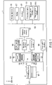
- FIG. 1 is a conceptual view showing an MRI apparatus including an arrayed structure according to an embodiment.
- an MRI apparatus 1 includes an arrayed structure 20, a static magnetic field magnet 101, a gradient magnetic field coil 103, a gradient magnetic field power supply 105, a couch 107, couch control circuitry 109, a transmitter/receiver coil 113, transmission circuitry 115, reception circuitry 119, sequence control circuitry 121, a bus 123, an interface 125, a display 127, a storage apparatus 129, and processing circuitry 131.
- the processing circuitry 131 includes a system control function 1311 and an image generation function 1313.
- the static magnetic field magnet 101, the gradient magnetic field coil, the arrayed structure 20, and the transmitter/receiver coil 113 are arranged in a gantry 150.
- the MRI apparatus 1 may include a hollow, cylindrical-shaped shim coil provided between the static magnetic field magnet 101 and the gradient magnetic field coil 103.
- the static magnetic field magnet 101 is a magnet formed in a hollow, approximately cylindrical shape.
- the static magnetic field magnet 101 is not necessarily in an approximately cylindrical shape, and may be formed in an open shape.
- the static magnetic field magnet 101 generates a uniform static magnetic field in the inner space.
- it is assumed that the static magnetic field magnet 101 is a superconducting magnet that uses a superconducting coil.
- the gradient magnetic field coil 103 is a coil formed in a hollow, cylindrical shape.
- the gradient magnetic field coil 103 is arranged inside the static magnetic field magnet 101.
- the gradient magnetic field coil 103 is formed of a combination of three coils respectively corresponding to X, Y, and Z axes that are orthogonal to each other.
- the Z-axis direction is defined as the same as the orientation of the static magnetic field.
- the Y-axis direction is a vertical direction
- the X-axis direction is a direction perpendicular to both the Z and Y axes.
- the three coils of the gradient magnetic field coil 103 individually receive an electric current from the gradient magnetic field power supply 105 and respectively generate gradient magnetic fields in which the magnetic field intensity changes along each of the X, Y and Z axes.
- the gradient magnetic fields along each of the X, Y, and Z axes generated by the gradient magnetic field coil 103 respectively form, for example, a gradient magnetic field for frequency encoding (readout gradient field), a gradient magnetic field for phase encoding, a gradient magnetic field for phase encoding, and a gradient magnetic field for slice selection.
- the gradient magnetic field for frequency encoding is employed to change the frequency of an MR signal emitted from a subject P in accordance with the spatial position.
- the gradient magnetic field for phase encoding is employed to change the phase of an MR signal in accordance with the spatial position.
- the gradient magnetic field for slice selection is employed to determine an imaging slice.
- the gradient magnetic field power supply 105 is a power supply apparatus that supplies an electric current to the gradient magnetic field coil 103 under the control of the sequence control circuitry 121.
- the couch 107 is an apparatus that includes a couch top 1071 on which a subject P is placed.
- the couch 107 inserts the couch top 1071 on which the subject P is placed into a bore 111, under the control of the couch control circuitry 109.
- the couch 107 is, for example, mounted in an examination room where the MRI apparatus 1 is mounted, in such a manner that the longitudinal axis of the couch 107 is parallel to the central axis of the static magnetic field magnet 101.
- the couch control circuitry 109 is circuitry that controls the couch 107, and drives the couch 107 in response to an operator's instructions via the interface 125, thereby moving the couch top 1071 in a longitudinal direction and a vertical direction.
- the transmitter/receiver coil 113 is an RF coil arranged inside the gradient magnetic field coil 103, and is, for example, a whole body coil.
- the transmitter/receiver coil 113 generates a transmit RF wave corresponding to a radio frequency magnetic field in response to a Radio Frequency (RF) pulse supplied from the transmission circuitry 115.
- the transmitter/receiver coil 113 receives an MR signal emitted from the subject P through the radio frequency magnetic field, and outputs the received MR signal to the reception circuitry 119.
- the arrayed structure 20 is arranged between the transmitter/receiver coil 113 and the gradient magnetic field coil 103 to improve the reception gain of the MR signal.
- the arrayed structure 20 will be discussed later with reference to FIG. 2 and the drawings that follow.
- the transmission circuitry 115 supplies an RF pulse corresponding to a Larmor frequency, etc. to the transmitter/receiver coil 113 under the control of the sequence control circuitry 121.
- the reception circuitry 119 generates, under the control of the sequence control circuitry 121, a digital MR signal, which is digitized complex data, based on the MR signal output from the transmitter/receiver coil 113. Specifically, the reception circuitry 119 subjects the MR signal to a variety of signal processing, and then performs analog-to-digital (A/D) conversion on data that has been subjected to the variety of signal processing. The reception circuitry 119 samples the A/D-converted data. Thereby, the reception circuitry 119 generates a digital MR signal (hereinafter referred to as "MR data"). The reception circuitry 119 outputs the generated MR data to the sequence control circuitry 121.
- MR data digital MR signal
- the sequence control circuitry 121 controls the gradient magnetic field power supply 105, the transmission circuitry 115, the reception circuitry 119, etc. in accordance with an examination protocol output from the processing circuitry 131, and performs imaging on the subject P.
- An examination protocol includes various pulse sequences (also referred to as "imaging sequences") corresponding to the examination.
- the examination protocol defines the magnitude of a current supplied from the gradient magnetic field power supply 105 to the gradient magnetic field coil 103, the timing of a supply of a current from the gradient magnetic field power supply 105 to the gradient magnetic field coil 103, the magnitude of an RF pulse supplied from the transmission circuitry 115 to the transmitter/receiver coil 113, the timing of a supply of an RF pulse from the transmission circuitry 115 to the transmitter/receiver coil 113, and the timing of reception of an MR signal at the transmitter/receiver coil 113, etc.
- the bus 123 is a transmission path for transmitting data between the interface 125, the display 127, the storage apparatus 129, and the processing circuitry 131.
- the bus 123 may be connected via, for example, a network to a variety of physiological signal measuring equipment, an external storage apparatus, and various modalities.
- an electrocardiograph (unillustrated) is connected to the bus as physiological signal measuring equipment.
- the interface 125 includes circuitry that receives various instructions and information inputs from an operator.
- the interface 125 includes, for example, circuitry relating to a pointing device such as a mouse or an input device such as a keyboard.
- the circuit included in the interface 125 is not limited to a circuit relating to a physical operational component, such as a mouse or a keyboard.
- the interface 125 may include an electrical signal processing circuit which receives an electrical signal corresponding to an input operation from external input equipment provided separately from the MRI apparatus 1 and outputs the received electrical signal to various circuits.
- the display 127 displays, for example, various magnetic resonance (MR) images generated by an image generation function 1313, and various types of information relating to imaging and image processing, under the control of a system control function 1311 in the processing circuitry 131.
- the display 127 is, for example, a CRT display, a liquid crystal display, an organic EL display, an LED display, a plasma display, or any other display or monitor known in the present technical field.
- the storage apparatus 129 stores, for example, MR data filled in k-space through the image generation function 1313 in the processing circuitry 131, and image data generated through the image generation function 1313.
- the storage apparatus 129 stores various types of examination protocols, conditions for imaging etc., including a plurality of imaging parameters that define examination protocols.
- the storage apparatus 129 stores programs corresponding to various functions executed by the processing circuitry 131.
- the storage apparatus 129 is, for example, a semiconductor memory element, such as a random access memory (RAM) and a flash memory, a hard disk drive, a solid-state drive, or an optical disk, etc.
- the storage apparatus 129 may also be, for example, a drive that reads and writes various kinds of information from and to a portable storage medium such as a CD-ROM drive, a DVD drive, or a flash memory.
- the processing circuitry 131 includes, as hardware resources, a processor (unillustrated) and a memory such as a read-only memory (ROM) and a RAM, and collectively controls the MRI apparatus 1.
- a processor unillustrated
- a memory such as a read-only memory (ROM) and a RAM
- processing circuitry 131 Such various functions of the processing circuitry 131 are stored in the storage apparatus 129 in the form of a program executable by a computer.
- the processing circuitry 131 is a processor which reads a program corresponding to these various respective functions from the storage apparatus 129 and executes the program to realize the function corresponding to the program.
- the processing circuitry 131 that has read each program is equipped with, for example, the functions shown in the processing circuitry 131 of FIG. 1 .
- FIG. 1 illustrates the case where the various functions are realized in a single piece of processing circuitry 131; however, the processing circuitry 131 may be configured by a combination of a plurality of independent processors, and the functions may be realized by the processors that execute the programs.
- each of the above-mentioned functions may be configured as a program, and a single piece of processing circuitry may execute each program, or a specific function may be implemented in exclusive, independent program-execution circuitry.
- processor means, for example, circuitry such as a central processing unit (CPU), a graphics processing unit (GPU), an application-specific integrated circuit (ASIC), or a programmable logic device (e.g., a simple programmable logic device (SPLD), a complex programmable logic device (CPLD), or a field-programmable gate array (FPGA).
- CPU central processing unit
- GPU graphics processing unit
- ASIC application-specific integrated circuit
- SPLD simple programmable logic device
- CPLD complex programmable logic device
- FPGA field-programmable gate array
- the processor reads and executes a program stored in the storage apparatus 129 to realize the corresponding function.
- a program may be directly integrated into the circuitry of the processor, instead of storing the program on the storage apparatus 129.
- the processor reads and executes a program integrated into the circuitry to realize the corresponding function.
- each of the couch control circuitry 109, the transmission circuitry 115, the reception circuitry 119, and the sequence control circuitry 121, etc. is also configured as an electronic circuit, such as the above processor.
- the processing circuitry 131 controls the MRI apparatus 1 through the system control function 1311. Specifically, the processing circuitry 131 reads a system control program stored in the storage apparatus 129 and expands it in the memory, and controls each circuitry of the MRI apparatus 1 in accordance with the expanded system control program. For example, the processing circuitry 131 reads an examination protocol from the storage apparatus 129 through the system control function 1311 based on an imaging condition input by the operator via the interface 125. The processing circuitry 131 may generate the examination protocol based on the imaging condition. The processing circuitry 131 transmits the examination protocol to the sequence control circuitry 121 to control imaging of the subject P.
- the processing circuitry 131 performs control through the system control function 1311 to apply an excitation pulse in accordance with the excitation pulse sequence and to apply a gradient magnetic field.
- the processing circuitry 131 causes the system control function 1311 to execute an excitation pulse sequence, and then collect an MR signal from the subject P in accordance with a data collection sequence, which is a pulse sequence for collecting various data, and thereby generates MR data.
- the system control function 1311 may be equipped with a function of performing a process similar to the sensor control unit 21.
- the processing circuitry 131 fills MR data along a readout direction of k-space in accordance with an intensity of the readout gradient field through the image generation function 1313.
- the processing circuitry 131 generates an MR image by performing a Fourier transform on the MR data filled in the k-space.
- the processing circuitry 131 can generate an absolute value (magnitude) image from complex MR data.
- the processing circuitry 131 can generate a phase image using real-part data and imaginary-part data in the complex MR data.
- the processing circuitry 131 outputs an MR image such as an absolute value image and a phase image to the display 127, the storage apparatus 129, etc.
- FIG. 2 is a perspective view of the arrayed structure 20.
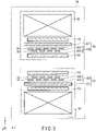
- FIG. 3 is a cross-sectional view of the gantry 150 of the MRI apparatus 1 taken along the z axis.
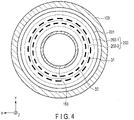
- FIG. 4 is a cross-sectional view of the gantry 150 of the MRI apparatus 1 taken along the x axis.
- the arrayed structure 20 is arranged on an inner peripheral side of the gradient magnetic field coil 103 and on an outer peripheral side of the transmitter/receiver coil 113.
- the arrayed structure 20 includes a conductor layer 201 and a layer stack 202.
- the conductor layer 201 is a cylindrical-shaped conductor arranged inside the gantry 150.
- the conductor layer 201 may be an RF shield that shields an RF signal stored in the gantry 150.
- the layer stack 202 is a cylindrical-shaped structure arranged on an inner peripheral side of the conductor layer 201, and is a "metasurface" in which a plurality of frequency selective surfaces (FSSs), on each of which a plurality of elements are periodically arranged, are stacked.
- FSSs frequency selective surfaces
- elements formed of metal conductors are periodically arranged on a flexible substrate formed in, for example, a cylindrical shape.
- first layer 202-1 a first frequency selective surface
- second layer 202-2 a second frequency selective surface
- each of the first layer 202-1 and the second layer 202-2 periodically arranged elements behave as "patches".
- the elements 31 arranged in the first layer 202-1 and the elements 32 arranged in the second layer 202-2 are arranged so as to be staggered when the outer peripheral direction is viewed from the central axis of the cylinder, namely, as viewed toward the outer peripheral direction from the center of the concentric circle in FIG. 3 or 4 .
- the elements 31 and 32 are arranged in such a manner that part of the element 31 formed in the first layer and part of the element 32 formed in the second layer overlap.
- the elements 31 and 32 are arranged in such a manner that, when the outer peripheral direction is viewed from the central axis of the cylinder, the center of each element 32 formed in the second layer overlaps a gap between the elements 31 periodically formed in the first layer.
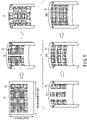
- FIG. 5(a) shows a case where the first layer 202-1 and the second layer 202-2 that form the layer stack 202 are stacked in a plane.
- an arrangement of the elements 51 is designed in a plane based on an applicable usage frequency of the arrayed structure 20 (hereinafter also referred to as "at the time of the planar design"), the size (area) and the interval of the periodic arrangement of the elements 51 are determined according to the applicable usage frequency. It is assumed that the elements 51 are shaped in a rectangle at the time of the planar design.
- the applicable usage frequency is, for example, a resonant frequency of electromagnetic waves corresponding to the magnetic field intensity used in the MRI apparatus.
- capacitance components and inductance components of the layer stack 202 at the time of the planar design are calculated. Specifically, a capacitance C V in a length direction and a capacitance C H in a circumferential direction of the layer stack 202, and an inductance L V in a length direction and an inductance L H in a circumferential direction of the layer stack 202 are calculated.
- the layer stack 202 is formed in a cylindrical shape with a desired curvature.
- the desired curvature is, for example, a curvature of a cylinder arranged in a space that is on an inner peripheral side of the gradient magnetic field coil 103 and on an outer peripheral side of the transmitter/receiver coil 113 in the gantry 150 of the MRI apparatus 1.
- the length of the circumference differs from layer to layer.
- the interval of the elements does not change in the length direction of the layer stack 202 from that at the time of the planar design; however, the interval of the elements 51 is widened in the circumferential direction of the layer stack 202, since the layer on the outer peripheral side has a longer circumference, as shown in FIG. 5(b1) . Accordingly, modifications as shown from FIG. 5(b1) to FIG. 5(b3) are assumed. A description from FIG. 5(b1) to FIG. 5(b3) will be given with reference to the first layer 202-1 as an example.
- the capacitance C H of a gap between the elements 51 in the circumferential direction decreases. If the size of the elements in the circumferential direction were increased to make the interval between the elements 51 in the circumferential direction revert to that at the time of the planar design, as shown in FIG. 5(b2) , the inductance L H in the circumferential direction would increase, while the inductance L V in the length direction would decrease. Also, the capacitance C V in the length direction would increase.
- the layer stack 202 when the layer stack 202 is ultimately designed in a cylindrical shape, offsets are provided in each element 51, as shown in FIG. 5(c) , and the area and the shape of each element of the first layer 202-1 and the second layer 202-2 are adjusted based on the curvature. Thereby, even when the layer stack 202 is formed in a cylindrical shape, the inductance components and the capacitance components can be designed to be approximately the same values as those at the time of the planar design.
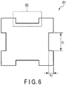
- FIG. 6 shows a single element 61 according to the first example.
- the element 61 is a patch obtained by forming a conductor in a planar shape, and is shaped in such a manner that at least a portion of each edge that faces another element 61 adjacent thereto in the layer is closer to the center of the element than the other portion of the edge.
- the center of the element is the central point of the element 61
- the element 61 is formed in such a manner that, when viewed from the top, at least a midpoint portion of each side is formed in a concave shape toward the central point of the element 61.
- the element 61 is shaped in a rectangle (quadrilateral) including an offset portion 62 at a central portion of each side.
- a size d 1 of the offset portion 62 of the element 61 namely, a size d 1 of a notch portion in a length direction and a depth d 2 of the offset portion 62 toward the center of the element, it is possible to adjust the capacitance components (C V and C H ).
- the capacitance components can be designed to be substantially the same values as those of the capacitance components at the time of the planar design.
- the layer stack 202 having a first example element shape will be described with reference to FIG. 7 .
- FIG. 7 shows a portion of the layer stack 202, with the lateral direction representing a circumferential direction and the vertical direction representing a length direction (z-axis direction) that is orthogonal to the circumferential direction.
- FIG. 7 shows an element arrangement of a first layer 202-1.
- the elements 61 of the first layer 202-1 have the shape shown in FIG. 6 , and are periodically arranged with a predetermined gap interposed therebetween.
- An offset portion 62 (notch portion) is formed at a central portion of each side of the element 61.
- FIG. 7 shows an element arrangement of the first layer 202-2
- the elements 71 of the second layer 202-2 are formed in a similar manner to the elements of the first layer 202-1.
- the right part of FIG. 7 shows a state of the layer stack 202 in which the first layer 202-1 and the second layer 202-2 are stacked in a cylindrical shape.
- the elements 71 of the second layer 202-2 are arranged in such a manner that the center of each element 71 is positioned at a gap between the elements 61 of the first layer 202-1.
- the elements 71 of the second layer 202-2 are arranged in such a manner that the center of each element 71 is positioned at a gap formed so as to be surrounded by four of the elements 61 of the first layer 202-1.
- the element arrangement in each layer is not limited to the positional relationship shown in the right part of FIG. 7 , and any arrangement may be adopted as long as the positional relationship is capable of appropriately controlling the phase of the usage frequency.
- analytical design can be performed through simulation based on, for example, design values of the capacitance components and the inductance components in the plane.
- inductance components and capacitance components can be designed to be similar to those at the time of the planar design, and phase characteristics that are desirable for the electromagnetic waves can be obtained. That is, a reflection signal obtained by letting an MR signal reflect off the conductive layer can be adjusted to be at the same phase as the MR signal directly received by the transmitter/receiver coil 113, thus improving the reception gain of the MR signal received by the transmitter/receiver coil 113. Since adjustment of the phase characteristics produces similar effects at the time of transmission of an RF signal, it is also possible to increase the signal intensity of an RF signal when the RF signal is transmitted from the transmitter/receiver coil 113.
- the order of designing the elements has been described from the point of view of convenience of explanation of changes in the inductance components and the capacitance components caused by a change in element shape; however, the order is not limited thereto.
- the planar design may be omitted, and the elements in the shape shown in FIG. 6 may be periodically arranged in a cylindrical-shaped layer stack 202, while analytically adjusting, through a simulation, the interval between the elements in the circumferential direction and the length direction and a size d 1 and a depth d 2 of offsets of the elements.
- FIG. 8 shows a single element 81 according to the second example.
- the element 81 is formed of a ring-shaped conductor, with sides 82 (longer sides of the rectangle) that are parallel to the circumferential direction having a width (thickness) greater than a width of sides 83 (shorter sides of the rectangle in this case) that are parallel to the length direction (z-axis direction) of the layer stack 202.
- sides 82 longer sides of the rectangle
- sides 83 shorter sides of the rectangle in this case
- FIG. 9 shows a portion of the layer stack 202, with the lateral direction representing a circumferential direction and the vertical direction representing a length direction (z-axis direction) that is orthogonal to the circumferential direction.
- the left part of FIG. 9 shows an arrangement of elements 81 of the first layer 202-1, and the central part of FIG. 9 shows an arrangement of the elements 91 of the second layer 202-2.
- the arrangement of the elements is similar to the arrangements shown in the left part and the central part of FIG. 7 , except that the shape of the elements differs.
- the right part of FIG. 9 shows a state of the layer stack 202 in which the first layer 202-1 and the second layer 202-2 are stacked in a cylindrical shape.
- the elements 91 of the second layer 202-2 are arranged in such a manner that the center of each element 91 is positioned at a gap between the elements 81 of the first layer 202-1.
- the layer stack 202 may be in a shape obtained by combining the element shapes of FIGS. 7 and 9 .
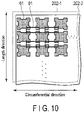
- An example of the layer stack 202 obtained by combining the first and second example element shapes will be described with reference to FIG. 10 .
- FIG. 10 shows a case where the first layer 202-1 has an element structure according to the first example shown in FIG. 6 , and the second layer 202-2 has an element structure according to the second example shown in FIG. 8 .
- the first layer 202-1 may have an element structure according to the second example shown in FIG. 8
- the second layer may have an element structure according to the first example shown in FIG. 6 .
- the layer stack 202 with different element structures as shown in FIG. 10 may be realized.
- the shape of the elements is not limited to the above-described ones, and any shape and periodic arrangement may be adopted as long as the values of the inductance component and the reactance component become substantially the same as those at the time of planar design when the layer stack 202 is formed in a cylindrical shape.
- Both the element 61 in the first example element shape and the element 81 in the second example element shape described above are assumed to be based on a rectangle (quadrilateral); however, the configuration is not limited thereto, and the element shape may be based on other polygons such as a hexagon and an octagon or may be based on a round shape such as a precise circle or an oval, or may be based on a complex shape in which part of the element includes a circular arc.
- FIG. 11 A first example element arrangement according to the modification is shown in FIG. 11 .
- the first layer 202-1 and the second layer 202-2 are not distinguished from each other for convenience in explanation; however, when they are stacked, they can be arranged in such a manner that the center of the element of the second layer 202-2 is positioned at a gap between elements of the first layer 202-1 when viewed from the outer circumferential direction from the central axis of the cylinder when a cylindrical shape is adopted, similarly to the above-described embodiment.
- FIG. 11 shows an example in which elements 1101 formed of hexagon-based conductors are arranged.
- Each element 1101 has a shape that includes an offset portion 1102 at a central part of each side that faces another element 1101 adjacent thereto in the layer.
- the element 1101 may be formed by offsetting the central part of each side of the hexagon-shaped conductor, or may be formed in such a manner that the central part becomes relatively offset by providing a projecting portion at each vertex of the hexagon-shaped conductor.
- the offset portion 1102 namely, the notch portion, is trapezoidal; however, the shape of the offset portion is not limited thereto, and may be a rectangular notch portion as shown in FIG. 6 .
- FIG. 12 a second example element arrangement according to the modification is shown in FIG. 12 .
- the elements 1101 are arranged in such a manner that their side portions (offset portions 1102) become parallel to the length direction, whereas in the second example element arrangement shown in FIG. 12 , the elements 1101 are arranged in such a manner that their side portions become parallel to the circumferential direction.
- FIG. 13 shows an arrangement in which the elements 1101 are arrayed in a diagonal orientation.
- the elements 1101 may be arrayed in any orientation.
- FIG. 14 a fourth example element arrangement according to the modification is shown in FIG. 14 .
- FIG. 14 shows a first modification of ring-shaped conductors according to the second example element shape, showing a case where each of a plurality of ring-shaped conductors 1400 is a conductor formed in the shape of a hexagonal ring.
- the elements 1400 are arranged in such a manner that their sides 1401 become parallel to the length direction.
- the elements 1400 are formed in such a manner that sides 1402 of the element 1400 that face another element 1400 adjacent thereto in the length direction and that extend in an approximately circumferential direction have a greater width than sides 1401 that are parallel to the length direction.
- wedge-shaped sides each formed of two continuous sides are formed to have a large thickness.
- sides 1402 that extend in the approximately circumferential direction are offset toward the center of the element.
- the size (depth) of the offset portion it is possible to adjust the capacitance components of a gap between the elements 1400 that are adjacent to each other in the length direction.
- the line width the inductance components in the circumferential direction can be adjusted.
- the length of sides 1401 that are parallel to the length direction the capacitance components in the circumferential direction can be adjusted.
- FIG. 15 a fifth example element arrangement according to the modification is shown in FIG. 15 .
- FIG. 15 shows a second modification of a ring-shaped conductor according to the second example element shape.
- the elements 1500 are arranged in such a manner that the sides 1501 become parallel to the circumferential direction.
- Sides 1501 of the element 1500 that face another element 1500 and that extend in parallel to the circumferential direction have a greater width than sides 1502 that are approximately parallel to the length direction. Also, sides 1501 that extend in parallel to the circumferential direction are offset toward the center of the element. By adjusting the size (depth) of the offset portion, it is possible to adjust the capacitance components of a gap between the elements 1500 that are adjacent to each other in the length direction. Moreover, by adjusting the line width of sides 1501, the inductance components in the circumferential direction can be adjusted. Furthermore, by adjusting the lengths of two sides 1502 that are approximately parallel to the length direction, the capacitance components in the circumferential direction can be adjusted.
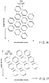
- the elements 1400 and the elements 1500, too, may be arrayed in a diagonal orientation.
- FIG. 16 shows a case where the elements 1400 are diagonally arrayed
- FIG. 17 shows a case where the elements 1500 are diagonally arrayed.
- the elements 1400 and the elements 1500 may be arranged in such a manner that they are tilted at a predetermined angle.
- a cylindrical-shaped arrayed structure which includes a conductor layer that is an RF shield and a structure in which a plurality of frequency selective surfaces designed for the usage frequency are stacked is formed, and elements of each frequency selective surface are formed in such a manner that at least a portion of each edge that faces an adjacent element in the layer is closer to the center of the element. It is thereby possible to adjust the phase characteristics of the usage frequency.
- a reflection signal obtained by letting an MR signal reflect off the conductive layer can be adjusted to be at the same phase as the MR signal directly received by the transmitter/receiver coil, and the reception gain of the MR signal received by the transmitter/receiver coil can be improved.
- This contributes to a workflow that enables examination without the need to mount a receiver coil on the subject P.
Landscapes
- Physics & Mathematics (AREA)
- Health & Medical Sciences (AREA)
- Life Sciences & Earth Sciences (AREA)
- Condensed Matter Physics & Semiconductors (AREA)
- General Physics & Mathematics (AREA)
- Engineering & Computer Science (AREA)
- Medical Informatics (AREA)
- Public Health (AREA)
- Biomedical Technology (AREA)
- Heart & Thoracic Surgery (AREA)
- Biophysics (AREA)
- Molecular Biology (AREA)
- Surgery (AREA)
- Animal Behavior & Ethology (AREA)
- General Health & Medical Sciences (AREA)
- Pathology (AREA)
- Veterinary Medicine (AREA)
- Nuclear Medicine, Radiotherapy & Molecular Imaging (AREA)
- Computer Networks & Wireless Communication (AREA)
- High Energy & Nuclear Physics (AREA)
- Radiology & Medical Imaging (AREA)
- Epidemiology (AREA)
- Magnetic Resonance Imaging Apparatus (AREA)
Abstract
According to one embodiment, an arrayed structure includes a cylindrical-shaped conductor layer and a cylindrical-shaped layer stack. The cylindrical-shaped layer stack is arranged on an inner periphery of the conductor layer and a plurality of frequency selective surfaces are stacked in the cylindrical-shaped layer stack. Each of the frequency selective surfaces has a plurality of elements which are periodically arranged. Each element of the plurality of elements is formed in such a manner that at least a portion of an edge of a first element that faces an adjacent element in the same layer is closer to a center of the first element than another portion of the edge.
Description
- This application is based upon and claims the benefit of priority from
Japanese Patent Application No. 2021-076424, filed April 28, 2021 2022-63602, filed April 6, 2022 - Embodiments described herein relate generally to an arrayed structure and a magnetic resonance imaging apparatus.
- In an existing magnetic resonance imaging apparatus, when a magnetic resonance (MR) signal from a subject is received by a whole body coil, which is a transmitter/receiver coil, the reception gain becomes insufficient. One of the reasons why the gain becomes insufficient is that, since a signal reflected from an RF shield arranged in an outer periphery of the whole body coil is phase-inverted, such a signal and the MR signal from the subject directly received by the receiver coil cancel each other out, causing a decrease in the gain.
- Thus, a receiver coil needs to be mounted on the subject; however, setting up a receiver coil by arranging it on the subject and connecting the receiver coil to the magnetic resonance imaging apparatus with the cable assembled on the coil is troublesome to the technician and is inefficient from the viewpoint of workflow. In addition, since a patient would feel discomfort with a receiver coil mounted on himself, it is ideal that the receiver coil not be used.
- In relation to foregoing embodiments, the following matters are disclosed as one aspect and selected features of the present invention.
- In an embodiment, a periodic structure includes: a cylindrical-shaped conductor layer; and a cylindrical-shaped layer stack which is arranged on an inner periphery of the conductor layer and in which a plurality of frequency selective surfaces are stacked, each of the frequency selective surfaces having a plurality of elements which are periodically arranged, and each element of the plurality of elements is formed in such a manner that at least a portion of an edge of a first element that faces an adjacent element in the same layer is closer to a center of the first element than another portion of the edge.
- In an embodiment, the element may be a conductor formed in a planar shape, and may be formed in such a manner that at least a portion of the edge is offset toward the center of the element.
- In an embodiment, the element may be a polygonal conductor, and may be formed in such a manner that a part of each side is offset toward a center of the element.
- In an embodiment, the element may be a ring-shaped conductor, and may be formed in such a manner that an edge that is parallel to a circumferential direction is offset toward a center of the element, and a width of the edge is greater than a width of a side that is orthogonal to the circumferential direction.
- In an embodiment, the ring-shaped conductor may be a polygon.
- In an embodiment, the polygon may be a quadrilateral or a hexagon.
- In an embodiment, the center of the element may be a central point of the element, and at least a midpoint portion of each edge may be formed in a concave shape intended toward the central point.
- In an embodiment, the elements may be arranged in such a manner that an inductance component and a capacitance component based on a planar arrangement of a layer stack that has been designed based on a usage frequency take values that are substantially identical to values of an inductance component and a capacitance component when the layer stack is formed in a cylindrical shape.
- In an embodiment, the he elements may be arranged in such a manner that, by adjusting an area based on a curvature of a cylinder formed of the layer stack, the inductance component and the capacitance component take values that are substantially identical to values of the inductance component and the capacitance component of the layer stack based on the planar arrangement.
- In an embodiment, the elements may be arranged in such a manner that, when an outer circumferential direction is viewed from a central axis of a cylinder formed of the layer stack, a part of an element formed in a first layer of the layer stack and a part of an element formed in a second layer of the layer stack overlap.
- In an embodiment, the elements may be arranged in such a manner that, when an outer peripheral direction is viewed from a central axis of a cylinder formed of the layer stack, a center of an element formed in a second layer is positioned at a gap between elements formed in the first layer of the layer stack, the second layer being arranged on an inner peripheral side of the first layer.
- In an embodiment, the element formed in a first layer of the layer stack may be formed as a quadrilateral conductor, with a part of each side being offset toward a center of the element. An element formed in a second layer of the layer stack is a rectangular, ring-shaped conductor, with a side parallel to a circumferential direction being offset toward the center of the element, a thickness of the side being greater than a thickness of a side that is orthogonal to the circumferential direction.
- In an embodiment, a magnetic resonance imaging apparatus includes: a gradient magnetic field coil; an arrayed structure according to any one of
Additional Notes 1 to 12, arranged on an inner periphery of the gradient magnetic field coil; and a transmitter/receiver coil arranged on an inner periphery of the arrayed structure and configured to transmit and receive an RF signal. - In an embodiment, element may be a quadrilateral conductor, with a notch being formed at a part of each side.
- In an embodiment, elements may be arranged in such a manner that, when an outer peripheral direction is viewed from a central axis of a cylinder formed of the layer stack, a center of an element formed in a second layer that is arranged on an inner peripheral side of the first layer overlaps a gap formed by four elements included in a plurality of elements formed in a first layer of the layer stack.
-
-
FIG. 1 is a conceptual view showing an MRI apparatus including an arrayed structure according to an embodiment. -
FIG. 2 is a perspective view showing details of the arrayed structure according to the embodiment. -
FIG. 3 is a cross-sectional view taken along a z-axis of a gantry of the MRI apparatus according to the embodiment. -
FIG. 4 is a cross-sectional view taken along an x-axis of the gantry of the MRI apparatus according to the embodiment. -
FIG. 5 is a conceptual view showing an example of a method of designing elements of a layer stack according to the embodiment. -
FIG. 6 is a diagram showing a first example element shape according to the embodiment. -
FIG. 7 is a diagram showing a layer stack having the first example element shape. -
FIG. 8 is a diagram showing a second example element shape according to the embodiment. -
FIG. 9 is a diagram showing a layer stack having the second example element shape according to the embodiment. -
FIG. 10 is a diagram showing an example of a layer stack in a shape obtained by combining the first and second example element shapes according to the embodiment. -
FIG. 11 is a diagram showing a first example element arrangement according to a modification. -
FIG. 12 is a diagram showing a second example element arrangement according to the modification. -
FIG. 13 is a diagram showing a third example element arrangement according to the modification. -
FIG. 14 is a diagram showing a fourth example element arrangement according to the modification. -
FIG. 15 is a diagram showing a fifth example element arrangement according to the modification. -
FIG. 16 is a diagram showing an example of a case whereelements 1401 are diagonally arrayed. -
FIG. 17 is a diagram showing an example of a case whereelements 1501 are diagonally arrayed. - In general, according to one embodiment, an arrayed structure includes a cylindrical-shaped conductor layer and a cylindrical-shaped layer stack. The cylindrical-shaped layer stack is arranged on an inner periphery of the conductor layer and a plurality of frequency selective surfaces are stacked in the cylindrical-shaped layer stack. Each of the frequency selective surfaces has a plurality of elements which is periodically arranged. Each element of the plurality of elements is formed in such a manner that at least a portion of an edge that faces an adjacent element in the same layers is closer to a center of the first element than another portion of the edge.
- Hereinafter, an arrayed structure and a magnetic resonance imaging (MRI) apparatus according to an embodiment will be described with reference to the accompanying drawings. In the embodiments described below, elements assigned the same reference symbols are assumed to perform the same operations, and redundant descriptions thereof will be omitted as appropriate.
-
FIG. 1 is a conceptual view showing an MRI apparatus including an arrayed structure according to an embodiment. - As shown in
FIG. 1 , anMRI apparatus 1 includes anarrayed structure 20, a staticmagnetic field magnet 101, a gradientmagnetic field coil 103, a gradient magneticfield power supply 105, acouch 107,couch control circuitry 109, a transmitter/receiver coil 113,transmission circuitry 115,reception circuitry 119,sequence control circuitry 121, abus 123, aninterface 125, adisplay 127, astorage apparatus 129, andprocessing circuitry 131. Theprocessing circuitry 131 includes asystem control function 1311 and animage generation function 1313. The staticmagnetic field magnet 101, the gradient magnetic field coil, thearrayed structure 20, and the transmitter/receiver coil 113 are arranged in agantry 150. TheMRI apparatus 1 may include a hollow, cylindrical-shaped shim coil provided between the staticmagnetic field magnet 101 and the gradientmagnetic field coil 103. - The static
magnetic field magnet 101 is a magnet formed in a hollow, approximately cylindrical shape. The staticmagnetic field magnet 101 is not necessarily in an approximately cylindrical shape, and may be formed in an open shape. The staticmagnetic field magnet 101 generates a uniform static magnetic field in the inner space. In the present embodiment, it is assumed that the staticmagnetic field magnet 101 is a superconducting magnet that uses a superconducting coil. - The gradient
magnetic field coil 103 is a coil formed in a hollow, cylindrical shape. The gradientmagnetic field coil 103 is arranged inside the staticmagnetic field magnet 101. The gradientmagnetic field coil 103 is formed of a combination of three coils respectively corresponding to X, Y, and Z axes that are orthogonal to each other. The Z-axis direction is defined as the same as the orientation of the static magnetic field. The Y-axis direction is a vertical direction, and the X-axis direction is a direction perpendicular to both the Z and Y axes. The three coils of the gradientmagnetic field coil 103 individually receive an electric current from the gradient magneticfield power supply 105 and respectively generate gradient magnetic fields in which the magnetic field intensity changes along each of the X, Y and Z axes. - The gradient magnetic fields along each of the X, Y, and Z axes generated by the gradient
magnetic field coil 103 respectively form, for example, a gradient magnetic field for frequency encoding (readout gradient field), a gradient magnetic field for phase encoding, a gradient magnetic field for phase encoding, and a gradient magnetic field for slice selection. The gradient magnetic field for frequency encoding is employed to change the frequency of an MR signal emitted from a subject P in accordance with the spatial position. The gradient magnetic field for phase encoding is employed to change the phase of an MR signal in accordance with the spatial position. The gradient magnetic field for slice selection is employed to determine an imaging slice. - The gradient magnetic
field power supply 105 is a power supply apparatus that supplies an electric current to the gradientmagnetic field coil 103 under the control of thesequence control circuitry 121. - The
couch 107 is an apparatus that includes acouch top 1071 on which a subject P is placed. Thecouch 107 inserts thecouch top 1071 on which the subject P is placed into abore 111, under the control of thecouch control circuitry 109. Thecouch 107 is, for example, mounted in an examination room where theMRI apparatus 1 is mounted, in such a manner that the longitudinal axis of thecouch 107 is parallel to the central axis of the staticmagnetic field magnet 101. - The
couch control circuitry 109 is circuitry that controls thecouch 107, and drives thecouch 107 in response to an operator's instructions via theinterface 125, thereby moving thecouch top 1071 in a longitudinal direction and a vertical direction. - The transmitter/
receiver coil 113 is an RF coil arranged inside the gradientmagnetic field coil 103, and is, for example, a whole body coil. The transmitter/receiver coil 113 generates a transmit RF wave corresponding to a radio frequency magnetic field in response to a Radio Frequency (RF) pulse supplied from thetransmission circuitry 115. The transmitter/receiver coil 113 receives an MR signal emitted from the subject P through the radio frequency magnetic field, and outputs the received MR signal to thereception circuitry 119. - The arrayed
structure 20 is arranged between the transmitter/receiver coil 113 and the gradientmagnetic field coil 103 to improve the reception gain of the MR signal. The arrayedstructure 20 will be discussed later with reference toFIG. 2 and the drawings that follow. - The
transmission circuitry 115 supplies an RF pulse corresponding to a Larmor frequency, etc. to the transmitter/receiver coil 113 under the control of thesequence control circuitry 121. - The
reception circuitry 119 generates, under the control of thesequence control circuitry 121, a digital MR signal, which is digitized complex data, based on the MR signal output from the transmitter/receiver coil 113. Specifically, thereception circuitry 119 subjects the MR signal to a variety of signal processing, and then performs analog-to-digital (A/D) conversion on data that has been subjected to the variety of signal processing. Thereception circuitry 119 samples the A/D-converted data. Thereby, thereception circuitry 119 generates a digital MR signal (hereinafter referred to as "MR data"). Thereception circuitry 119 outputs the generated MR data to thesequence control circuitry 121. - The
sequence control circuitry 121 controls the gradient magneticfield power supply 105, thetransmission circuitry 115, thereception circuitry 119, etc. in accordance with an examination protocol output from theprocessing circuitry 131, and performs imaging on the subject P. An examination protocol includes various pulse sequences (also referred to as "imaging sequences") corresponding to the examination. The examination protocol defines the magnitude of a current supplied from the gradient magneticfield power supply 105 to the gradientmagnetic field coil 103, the timing of a supply of a current from the gradient magneticfield power supply 105 to the gradientmagnetic field coil 103, the magnitude of an RF pulse supplied from thetransmission circuitry 115 to the transmitter/receiver coil 113, the timing of a supply of an RF pulse from thetransmission circuitry 115 to the transmitter/receiver coil 113, and the timing of reception of an MR signal at the transmitter/receiver coil 113, etc. - The
bus 123 is a transmission path for transmitting data between theinterface 125, thedisplay 127, thestorage apparatus 129, and theprocessing circuitry 131. Thebus 123 may be connected via, for example, a network to a variety of physiological signal measuring equipment, an external storage apparatus, and various modalities. For example, an electrocardiograph (unillustrated) is connected to the bus as physiological signal measuring equipment. - The
interface 125 includes circuitry that receives various instructions and information inputs from an operator. Theinterface 125 includes, for example, circuitry relating to a pointing device such as a mouse or an input device such as a keyboard. The circuit included in theinterface 125 is not limited to a circuit relating to a physical operational component, such as a mouse or a keyboard. For example, theinterface 125 may include an electrical signal processing circuit which receives an electrical signal corresponding to an input operation from external input equipment provided separately from theMRI apparatus 1 and outputs the received electrical signal to various circuits. - The
display 127 displays, for example, various magnetic resonance (MR) images generated by animage generation function 1313, and various types of information relating to imaging and image processing, under the control of asystem control function 1311 in theprocessing circuitry 131. Thedisplay 127 is, for example, a CRT display, a liquid crystal display, an organic EL display, an LED display, a plasma display, or any other display or monitor known in the present technical field. - The
storage apparatus 129 stores, for example, MR data filled in k-space through theimage generation function 1313 in theprocessing circuitry 131, and image data generated through theimage generation function 1313. Thestorage apparatus 129 stores various types of examination protocols, conditions for imaging etc., including a plurality of imaging parameters that define examination protocols. Thestorage apparatus 129 stores programs corresponding to various functions executed by theprocessing circuitry 131. Thestorage apparatus 129 is, for example, a semiconductor memory element, such as a random access memory (RAM) and a flash memory, a hard disk drive, a solid-state drive, or an optical disk, etc. Thestorage apparatus 129 may also be, for example, a drive that reads and writes various kinds of information from and to a portable storage medium such as a CD-ROM drive, a DVD drive, or a flash memory. - The
processing circuitry 131 includes, as hardware resources, a processor (unillustrated) and a memory such as a read-only memory (ROM) and a RAM, and collectively controls theMRI apparatus 1. - Such various functions of the
processing circuitry 131 are stored in thestorage apparatus 129 in the form of a program executable by a computer. Theprocessing circuitry 131 is a processor which reads a program corresponding to these various respective functions from thestorage apparatus 129 and executes the program to realize the function corresponding to the program. In other words, theprocessing circuitry 131 that has read each program is equipped with, for example, the functions shown in theprocessing circuitry 131 ofFIG. 1 . -
FIG. 1 illustrates the case where the various functions are realized in a single piece ofprocessing circuitry 131; however, theprocessing circuitry 131 may be configured by a combination of a plurality of independent processors, and the functions may be realized by the processors that execute the programs. In other words, each of the above-mentioned functions may be configured as a program, and a single piece of processing circuitry may execute each program, or a specific function may be implemented in exclusive, independent program-execution circuitry. - The term "processor" used in the above explanation means, for example, circuitry such as a central processing unit (CPU), a graphics processing unit (GPU), an application-specific integrated circuit (ASIC), or a programmable logic device (e.g., a simple programmable logic device (SPLD), a complex programmable logic device (CPLD), or a field-programmable gate array (FPGA).
- The processor reads and executes a program stored in the
storage apparatus 129 to realize the corresponding function. A program may be directly integrated into the circuitry of the processor, instead of storing the program on thestorage apparatus 129. In this case, the processor reads and executes a program integrated into the circuitry to realize the corresponding function. Similarly, each of thecouch control circuitry 109, thetransmission circuitry 115, thereception circuitry 119, and thesequence control circuitry 121, etc. is also configured as an electronic circuit, such as the above processor. - The
processing circuitry 131 controls theMRI apparatus 1 through thesystem control function 1311. Specifically, theprocessing circuitry 131 reads a system control program stored in thestorage apparatus 129 and expands it in the memory, and controls each circuitry of theMRI apparatus 1 in accordance with the expanded system control program. For example, theprocessing circuitry 131 reads an examination protocol from thestorage apparatus 129 through thesystem control function 1311 based on an imaging condition input by the operator via theinterface 125. Theprocessing circuitry 131 may generate the examination protocol based on the imaging condition. Theprocessing circuitry 131 transmits the examination protocol to thesequence control circuitry 121 to control imaging of the subject P. - The
processing circuitry 131 performs control through thesystem control function 1311 to apply an excitation pulse in accordance with the excitation pulse sequence and to apply a gradient magnetic field. Theprocessing circuitry 131 causes thesystem control function 1311 to execute an excitation pulse sequence, and then collect an MR signal from the subject P in accordance with a data collection sequence, which is a pulse sequence for collecting various data, and thereby generates MR data. Thesystem control function 1311 may be equipped with a function of performing a process similar to the sensor control unit 21. - The
processing circuitry 131 fills MR data along a readout direction of k-space in accordance with an intensity of the readout gradient field through theimage generation function 1313. Theprocessing circuitry 131 generates an MR image by performing a Fourier transform on the MR data filled in the k-space. For example, theprocessing circuitry 131 can generate an absolute value (magnitude) image from complex MR data. Also, theprocessing circuitry 131 can generate a phase image using real-part data and imaginary-part data in the complex MR data. Theprocessing circuitry 131 outputs an MR image such as an absolute value image and a phase image to thedisplay 127, thestorage apparatus 129, etc. - Next, details of the arrayed
structure 20 will be described with reference toFIGS. 2 to 4 . -
FIG. 2 is a perspective view of the arrayedstructure 20.FIG. 3 is a cross-sectional view of thegantry 150 of theMRI apparatus 1 taken along the z axis.FIG. 4 is a cross-sectional view of thegantry 150 of theMRI apparatus 1 taken along the x axis. - The arrayed
structure 20 is arranged on an inner peripheral side of the gradientmagnetic field coil 103 and on an outer peripheral side of the transmitter/receiver coil 113. The arrayedstructure 20 includes aconductor layer 201 and alayer stack 202. - The
conductor layer 201 is a cylindrical-shaped conductor arranged inside thegantry 150. Theconductor layer 201 may be an RF shield that shields an RF signal stored in thegantry 150. - The
layer stack 202 is a cylindrical-shaped structure arranged on an inner peripheral side of theconductor layer 201, and is a "metasurface" in which a plurality of frequency selective surfaces (FSSs), on each of which a plurality of elements are periodically arranged, are stacked. In each frequency selective surface that forms a metasurface, elements formed of metal conductors are periodically arranged on a flexible substrate formed in, for example, a cylindrical shape. By changing the shape and arrangement of the elements, it is possible to selectively change and control the frequency, amplitude, and phase of electromagnetic waves reflected from theconductor layer 201. That is, when the arrayedstructure 20 is installed in theMRI apparatus 1, it is possible to control the phase when an MR signal emitted from the subject P is reflected by theconductor layer 201. - In the present embodiment, an example is shown in which two layers, namely, a first frequency selective surface (hereinafter referred to as "first layer 202-1") and a second frequency selective surface (hereinafter referred to as "second layer 202-2") arranged on an inner peripheral side of the first layer 202-1 are stacked; however, the configuration is not limited thereto, and two or more layers may be stacked. In addition, a material such as a dielectric material may be inserted between the substrates or the stacked layers.
- In each of the first layer 202-1 and the second layer 202-2, periodically arranged elements behave as "patches". The
elements 31 arranged in the first layer 202-1 and theelements 32 arranged in the second layer 202-2 are arranged so as to be staggered when the outer peripheral direction is viewed from the central axis of the cylinder, namely, as viewed toward the outer peripheral direction from the center of the concentric circle inFIG. 3 or4 . For example, theelements element 31 formed in the first layer and part of theelement 32 formed in the second layer overlap. More specifically, theelements element 32 formed in the second layer overlaps a gap between theelements 31 periodically formed in the first layer. - Next, an example of a method of designing the elements of the
layer stack 202 will be described with reference to the conceptual view ofFIG. 5 . -
FIG. 5(a) shows a case where the first layer 202-1 and the second layer 202-2 that form thelayer stack 202 are stacked in a plane. When an arrangement of theelements 51 is designed in a plane based on an applicable usage frequency of the arrayed structure 20 (hereinafter also referred to as "at the time of the planar design"), the size (area) and the interval of the periodic arrangement of theelements 51 are determined according to the applicable usage frequency. It is assumed that theelements 51 are shaped in a rectangle at the time of the planar design. - The applicable usage frequency is, for example, a resonant frequency of electromagnetic waves corresponding to the magnetic field intensity used in the MRI apparatus. Also, capacitance components and inductance components of the
layer stack 202 at the time of the planar design are calculated. Specifically, a capacitance CV in a length direction and a capacitance CH in a circumferential direction of thelayer stack 202, and an inductance LV in a length direction and an inductance LH in a circumferential direction of thelayer stack 202 are calculated. - Next, as shown in
FIG. 5(b) , it is assumed that thelayer stack 202 is formed in a cylindrical shape with a desired curvature. The desired curvature is, for example, a curvature of a cylinder arranged in a space that is on an inner peripheral side of the gradientmagnetic field coil 103 and on an outer peripheral side of the transmitter/receiver coil 113 in thegantry 150 of theMRI apparatus 1. When the planar-shapedlayer stack 202 is formed into a cylindrical shape, the length of the circumference differs from layer to layer. Specifically, the interval of the elements does not change in the length direction of thelayer stack 202 from that at the time of the planar design; however, the interval of theelements 51 is widened in the circumferential direction of thelayer stack 202, since the layer on the outer peripheral side has a longer circumference, as shown inFIG. 5(b1) . Accordingly, modifications as shown fromFIG. 5(b1) to FIG. 5(b3) are assumed. A description fromFIG. 5(b1) to FIG. 5(b3) will be given with reference to the first layer 202-1 as an example. - As an interval in the circumferential direction increases, the capacitance CH of a gap between the
elements 51 in the circumferential direction decreases. If the size of the elements in the circumferential direction were increased to make the interval between theelements 51 in the circumferential direction revert to that at the time of the planar design, as shown inFIG. 5(b2) , the inductance LH in the circumferential direction would increase, while the inductance LV in the length direction would decrease. Also, the capacitance CV in the length direction would increase. - By increasing the size of the elements in the length direction while maintaining the size of the elements in the circumferential direction, as shown in
FIG. 5(b3) , it is possible to make adjustments in such a manner that the inductance LV in the length direction increases and the inductance LH in the circumferential direction decreases. Thereby, it is possible to make the values of the inductance LV and the inductance LH revert to those at the time of the planar design. However, the increase in the lengths of the sides and the decrease in the interval between the elements cause an increase in the capacitance components (CV and CH). - Thus, when the
layer stack 202 is ultimately designed in a cylindrical shape, offsets are provided in eachelement 51, as shown inFIG. 5(c) , and the area and the shape of each element of the first layer 202-1 and the second layer 202-2 are adjusted based on the curvature. Thereby, even when thelayer stack 202 is formed in a cylindrical shape, the inductance components and the capacitance components can be designed to be approximately the same values as those at the time of the planar design. - More specifically, a first example element shape will be described with reference to
FIG. 6 . -
FIG. 6 shows asingle element 61 according to the first example. Theelement 61 is a patch obtained by forming a conductor in a planar shape, and is shaped in such a manner that at least a portion of each edge that faces anotherelement 61 adjacent thereto in the layer is closer to the center of the element than the other portion of the edge. In other words, the center of the element is the central point of theelement 61, and theelement 61 is formed in such a manner that, when viewed from the top, at least a midpoint portion of each side is formed in a concave shape toward the central point of theelement 61. In other words, theelement 61 is shaped in a rectangle (quadrilateral) including an offsetportion 62 at a central portion of each side. By adjusting a size d1 of the offsetportion 62 of theelement 61, namely, a size d1 of a notch portion in a length direction and a depth d2 of the offsetportion 62 toward the center of the element, it is possible to adjust the capacitance components (CV and CH). Thereby, even when thelayer stack 202 is formed in a cylindrical shape, the capacitance components can be designed to be substantially the same values as those of the capacitance components at the time of the planar design. - Next, the
layer stack 202 having a first example element shape will be described with reference toFIG. 7 . -
FIG. 7 shows a portion of thelayer stack 202, with the lateral direction representing a circumferential direction and the vertical direction representing a length direction (z-axis direction) that is orthogonal to the circumferential direction. - The left part of
FIG. 7 shows an element arrangement of a first layer 202-1. Theelements 61 of the first layer 202-1 have the shape shown inFIG. 6 , and are periodically arranged with a predetermined gap interposed therebetween. An offset portion 62 (notch portion) is formed at a central portion of each side of theelement 61. - The central part of
FIG. 7 shows an element arrangement of the first layer 202-2 Theelements 71 of the second layer 202-2 are formed in a similar manner to the elements of the first layer 202-1. - The right part of
FIG. 7 shows a state of thelayer stack 202 in which the first layer 202-1 and the second layer 202-2 are stacked in a cylindrical shape. Thus, when the first layer 202-1 and the second layer 202-2 are viewed from a stacking direction in which they are stacked, namely, when viewed from an outer peripheral direction with respect to a central axis of a cylinder when they are cylindrically shaped, theelements 71 of the second layer 202-2 are arranged in such a manner that the center of eachelement 71 is positioned at a gap between theelements 61 of the first layer 202-1. More specifically, theelements 71 of the second layer 202-2 are arranged in such a manner that the center of eachelement 71 is positioned at a gap formed so as to be surrounded by four of theelements 61 of the first layer 202-1. The element arrangement in each layer is not limited to the positional relationship shown in the right part ofFIG. 7 , and any arrangement may be adopted as long as the positional relationship is capable of appropriately controlling the phase of the usage frequency. - In the step of designing the
layer stack 202 shown in the right side ofFIG. 7 , analytical design can be performed through simulation based on, for example, design values of the capacitance components and the inductance components in the plane. In this manner, even when thelayer stack 202 is formed in a cylindrical shape, inductance components and capacitance components can be designed to be similar to those at the time of the planar design, and phase characteristics that are desirable for the electromagnetic waves can be obtained. That is, a reflection signal obtained by letting an MR signal reflect off the conductive layer can be adjusted to be at the same phase as the MR signal directly received by the transmitter/receiver coil 113, thus improving the reception gain of the MR signal received by the transmitter/receiver coil 113. Since adjustment of the phase characteristics produces similar effects at the time of transmission of an RF signal, it is also possible to increase the signal intensity of an RF signal when the RF signal is transmitted from the transmitter/receiver coil 113. - In
FIG. 5 , the order of designing the elements has been described from the point of view of convenience of explanation of changes in the inductance components and the capacitance components caused by a change in element shape; however, the order is not limited thereto. For example, the planar design may be omitted, and the elements in the shape shown inFIG. 6 may be periodically arranged in a cylindrical-shapedlayer stack 202, while analytically adjusting, through a simulation, the interval between the elements in the circumferential direction and the length direction and a size d1 and a depth d2 of offsets of the elements. - Next, a second example element shape will be described with reference to
FIG. 8 . -
FIG. 8 shows asingle element 81 according to the second example. Theelement 81 is formed of a ring-shaped conductor, with sides 82 (longer sides of the rectangle) that are parallel to the circumferential direction having a width (thickness) greater than a width of sides 83 (shorter sides of the rectangle in this case) that are parallel to the length direction (z-axis direction) of thelayer stack 202. In the example ofFIG. 8 , it is assumed that the ring-shaped conductor is a rectangle (quadrilateral). -
Sides 82 that are parallel to the circumferential direction are offset toward the center of the element. Thereby, the capacitance component CV in the length direction can be decreased. At this time, even when theside 82 is offset, the inductance components (LV and LH) and the capacitance CH in the circumferential direction do not change. By adjusting a width d3 of theside 82, it is possible to adjust only the inductance LH in the circumferential direction. As a result, the inductance components and the capacitance components can be easily adjusted. - Next, a
layer stack 202 having the second example element shape will be described with reference toFIG. 9 . - Similarly to
FIG. 7 ,FIG. 9 shows a portion of thelayer stack 202, with the lateral direction representing a circumferential direction and the vertical direction representing a length direction (z-axis direction) that is orthogonal to the circumferential direction. - The left part of
FIG. 9 shows an arrangement ofelements 81 of the first layer 202-1, and the central part ofFIG. 9 shows an arrangement of theelements 91 of the second layer 202-2. The arrangement of the elements is similar to the arrangements shown in the left part and the central part ofFIG. 7 , except that the shape of the elements differs. - Similarly to the right part of
FIG. 7 , the right part ofFIG. 9 shows a state of thelayer stack 202 in which the first layer 202-1 and the second layer 202-2 are stacked in a cylindrical shape. In the case of the second example element shape, too, when the first layer 202-1 and the second layer 202-2 are viewed from a stacking direction in which they are stacked, namely, when viewed from an outer peripheral direction from a central axis of a cylinder when they are cylindrically shaped, theelements 91 of the second layer 202-2 are arranged in such a manner that the center of eachelement 91 is positioned at a gap between theelements 81 of the first layer 202-1. - The
layer stack 202 may be in a shape obtained by combining the element shapes ofFIGS. 7 and9 . An example of thelayer stack 202 obtained by combining the first and second example element shapes will be described with reference toFIG. 10 . -
FIG. 10 shows a case where the first layer 202-1 has an element structure according to the first example shown inFIG. 6 , and the second layer 202-2 has an element structure according to the second example shown inFIG. 8 . In contrast, the first layer 202-1 may have an element structure according to the second example shown inFIG. 8 , and the second layer may have an element structure according to the first example shown inFIG. 6 . - By designing in advance an arrangement of elements in a state in which layers with different element structures are stacked at the time of design of frequency selective surfaces with respect to the usage frequency, the
layer stack 202 with different element structures as shown inFIG. 10 may be realized. - The shape of the elements is not limited to the above-described ones, and any shape and periodic arrangement may be adopted as long as the values of the inductance component and the reactance component become substantially the same as those at the time of planar design when the
layer stack 202 is formed in a cylindrical shape. - Both the
element 61 in the first example element shape and theelement 81 in the second example element shape described above are assumed to be based on a rectangle (quadrilateral); however, the configuration is not limited thereto, and the element shape may be based on other polygons such as a hexagon and an octagon or may be based on a round shape such as a precise circle or an oval, or may be based on a complex shape in which part of the element includes a circular arc. - A first example element arrangement according to the modification is shown in
FIG. 11 . In the modification shown inFIG. 11 and the drawings that follow, the first layer 202-1 and the second layer 202-2 are not distinguished from each other for convenience in explanation; however, when they are stacked, they can be arranged in such a manner that the center of the element of the second layer 202-2 is positioned at a gap between elements of the first layer 202-1 when viewed from the outer circumferential direction from the central axis of the cylinder when a cylindrical shape is adopted, similarly to the above-described embodiment. -
FIG. 11 shows an example in whichelements 1101 formed of hexagon-based conductors are arranged. Eachelement 1101 has a shape that includes an offsetportion 1102 at a central part of each side that faces anotherelement 1101 adjacent thereto in the layer. Theelement 1101 may be formed by offsetting the central part of each side of the hexagon-shaped conductor, or may be formed in such a manner that the central part becomes relatively offset by providing a projecting portion at each vertex of the hexagon-shaped conductor. - By adjusting the size of the vertex portion (or the projecting portion if the projecting portion is provided) and the size of the offset
portion 1102, it is possible to adjust the capacitance component and the inductance component. Herein, the offsetportion 1102, namely, the notch portion, is trapezoidal; however, the shape of the offset portion is not limited thereto, and may be a rectangular notch portion as shown inFIG. 6 . - Next, a second example element arrangement according to the modification is shown in
FIG. 12 . - In the first example element arrangement shown in
FIG. 11 , a case is shown where theelements 1101 are arranged in such a manner that their side portions (offset portions 1102) become parallel to the length direction, whereas in the second example element arrangement shown inFIG. 12 , theelements 1101 are arranged in such a manner that their side portions become parallel to the circumferential direction. - A third example element arrangement according to the modification is shown in
FIG. 13. FIG. 13 shows an arrangement in which theelements 1101 are arrayed in a diagonal orientation. - As shown in
FIGS. 12 and13 , theelements 1101 may be arrayed in any orientation. - Next, a fourth example element arrangement according to the modification is shown in
FIG. 14 . -
FIG. 14 shows a first modification of ring-shaped conductors according to the second example element shape, showing a case where each of a plurality of ring-shapedconductors 1400 is a conductor formed in the shape of a hexagonal ring. Theelements 1400 are arranged in such a manner that theirsides 1401 become parallel to the length direction. Theelements 1400 are formed in such a manner that sides 1402 of theelement 1400 that face anotherelement 1400 adjacent thereto in the length direction and that extend in an approximately circumferential direction have a greater width thansides 1401 that are parallel to the length direction. Herein, wedge-shaped sides each formed of two continuous sides are formed to have a large thickness. - Also, sides 1402 that extend in the approximately circumferential direction are offset toward the center of the element. By adjusting the size (depth) of the offset portion, it is possible to adjust the capacitance components of a gap between the
elements 1400 that are adjacent to each other in the length direction. Moreover, by adjusting the line width, the inductance components in the circumferential direction can be adjusted. Furthermore, by adjusting the length ofsides 1401 that are parallel to the length direction, the capacitance components in the circumferential direction can be adjusted. - Next, a fifth example element arrangement according to the modification is shown in
FIG. 15 . -
FIG. 15 shows a second modification of a ring-shaped conductor according to the second example element shape. In this example, theelements 1500 are arranged in such a manner that thesides 1501 become parallel to the circumferential direction. -
Sides 1501 of theelement 1500 that face anotherelement 1500 and that extend in parallel to the circumferential direction have a greater width thansides 1502 that are approximately parallel to the length direction. Also, sides 1501 that extend in parallel to the circumferential direction are offset toward the center of the element. By adjusting the size (depth) of the offset portion, it is possible to adjust the capacitance components of a gap between theelements 1500 that are adjacent to each other in the length direction. Moreover, by adjusting the line width ofsides 1501, the inductance components in the circumferential direction can be adjusted. Furthermore, by adjusting the lengths of twosides 1502 that are approximately parallel to the length direction, the capacitance components in the circumferential direction can be adjusted. - The
elements 1400 and theelements 1500, too, may be arrayed in a diagonal orientation. -
FIG. 16 shows a case where theelements 1400 are diagonally arrayed, andFIG. 17 shows a case where theelements 1500 are diagonally arrayed. In this manner, theelements 1400 and theelements 1500 may be arranged in such a manner that they are tilted at a predetermined angle. - According to the above-described embodiment, a cylindrical-shaped arrayed structure which includes a conductor layer that is an RF shield and a structure in which a plurality of frequency selective surfaces designed for the usage frequency are stacked is formed, and elements of each frequency selective surface are formed in such a manner that at least a portion of each edge that faces an adjacent element in the layer is closer to the center of the element. It is thereby possible to adjust the phase characteristics of the usage frequency. In particular, by arranging an arrayed structure on an outer peripheral side of a transmitter/receiver coil (whole body coil) in an MRI apparatus, a reflection signal obtained by letting an MR signal reflect off the conductive layer can be adjusted to be at the same phase as the MR signal directly received by the transmitter/receiver coil, and the reception gain of the MR signal received by the transmitter/receiver coil can be improved. This contributes to a workflow that enables examination without the need to mount a receiver coil on the subject P.
- According to at least one of the above-described embodiments, it is possible to improve the reception gain.
- While certain embodiments have been described, these embodiments have been presented by way of example only, and are not intended to limit the scope of the inventions. Indeed, the novel embodiments described herein may be embodied in a variety of other forms; furthermore, various omissions, substitutions and changes in the form of the embodiments described herein may be made without departing from the scope of the invention as defined by the appended claims.
Claims (14)
- An arrayed structure (20) comprising:a cylindrical-shaped conductor layer (201); anda cylindrical-shaped layer stack (202) which is arranged on an inner periphery of the conductor layer (201) and in which a plurality of frequency selective surfaces are stacked, each of the frequency selective surfaces having a plurality of elements (31, 32, 51, 61, 71, 81, 91, 1101, 1400, 1500) which are periodically arranged, wherein each element (31, 32, 51, 61, 71, 81, 91, 1101, 1400, 1500) of the plurality of elements (31, 32, 51, 61, 71, 81, 91, 1101, 1400, 1500) is formed in such a manner that at least a portion of an edge that faces an adjacent element (31, 32, 51, 61, 71, 81, 91, 1101, 1400, 1500) in the same layer is closer to a center of the first element than another portion of the edge.
- The arrayed structure according to claim 1, wherein the element (31, 32, 61, 71) is a conductor formed in a planar shape, and is formed in such a manner that at least a portion of the edge is offset toward the center of the element.
- The arrayed structure according to claim 1, wherein the element (1101, 1400, 1500) is a polygonal conductor, and is formed in such a manner that a portion of each side is offset toward the center of the element.
- The arrayed structure according to claim 1, wherein the element is a ring-shaped conductor (81, 91, 1400, 1500), and is formed in such a manner that an edge that is parallel to a circumferential direction is offset toward the center of the element (81, 91), and a width of the edge is greater than a width of a side that is orthogonal to the circumferential direction.
- The arrayed structure according to claim 4, wherein the ring-shaped conductor is a polygon.
- The arrayed structure according to claim 3, wherein the polygon is a quadrilateral or a hexagon.
- The arrayed structure according to claim 5, wherein the polygon is a quadrilateral or a hexagon.
- The arrayed structure according to claim 1, whereinthe center of the element (31, 32, 51, 61, 71, 81, 91, 1101, 1400, 1500) is a central point of the element (31, 32, 51, 61, 71, 81, 91, 1101, 1400, 1500), andat least a midpoint portion of each edge is formed in a concave shape indented toward the central point.
- The arrayed structure according to any preceding claim, wherein the elements (31, 32, 51, 61, 71, 81, 91, 1101, 1400, 1500) are arranged in such a manner that an inductance component and a capacitance component of the layer stack (202) based on a planar arrangement of a layer stack that has been designed based on a usage frequency take values that are substantially identical to values of an inductance component and a capacitance component when the layer stack is formed in a cylindrical shape.
- The arrayed structure according to claim 9, wherein the elements (31, 32, 51, 61, 71, 81, 91, 1101, 1400, 1500) are arranged in such a manner that, by adjusting an area based on a curvature of a cylinder formed of the layer stack, the inductance component and the capacitance component take values that are substantially identical to values of the inductance component and the capacitance component based on the planar arrangement.
- The arrayed structure according to any of claims 1 to 4, wherein the elements are arranged in such a manner that, when an outer circumferential direction is viewed from a central axis of a cylinder formed of the layer stack, a part of an element (31, 32, 51, 61, 71, 1101) formed in a first layer of the layer stack and a part of an element formed in a second layer of the layer stack overlap.
- The arrayed structure according to any preceding claim, wherein the elements (31, 32, 51, 61, 71, 81, 91, 1101, 1400, 1500) are arranged in such a manner that, when an outer peripheral direction is viewed from a central axis of a cylinder formed of the layer stack, the center of the element formed in a second layer (202-2) is positioned at a gap between elements (31, 32, 51, 61, 71, 81, 91, 1101, 1400, 1500) formed in the first layer (202-1) of the layer stack (202), the second layer (202-1) being arranged on an inner peripheral side of the first layer.
- The arrayed structure according to claim 1, whereinan element (31, 32, 51, 61, 71) formed in a first layer (202-1) of the layer stack (202) is a quadrilateral conductor, with a part of each side being offset toward the center of the element (31, 32, 51, 61, 71), andan element formed in a second layer (202-2) of the layer stack (202) is a rectangular, ring-shaped conductor (91), with a side parallel to a circumferential direction being offset toward the center of the element (91), a thickness of the side being greater than a thickness of a side that is orthogonal to the circumferential direction.
- A magnetic resonance imaging apparatus comprising:a gradient magnetic field coil (103);an arrayed structure according to any preceding claims, arranged on an inner periphery of the gradient magnetic field coil (103); anda transmitter/receiver coil (113) arranged on an inner periphery of the arrayed structure and configured to transmit and receive an RF signal.
Applications Claiming Priority (2)
| Application Number | Priority Date | Filing Date | Title |
|---|---|---|---|
| JP2021076424 | 2021-04-28 | ||
| JP2022063602A JP7817052B2 (en) | 2021-04-28 | 2022-04-06 | Periodic structure and magnetic resonance imaging device |
Publications (1)
| Publication Number | Publication Date |
|---|---|
| EP4083649A1 true EP4083649A1 (en) | 2022-11-02 |
Family
ID=81307284
Family Applications (1)
| Application Number | Title | Priority Date | Filing Date |
|---|---|---|---|
| EP22167967.3A Pending EP4083649A1 (en) | 2021-04-28 | 2022-04-12 | Arrayed structure and magnetic resonance imaging apparatus |
Country Status (3)
| Country | Link |
|---|---|
| US (1) | US11921175B2 (en) |
| EP (1) | EP4083649A1 (en) |
| CN (1) | CN115245323B (en) |
Citations (2)
| Publication number | Priority date | Publication date | Assignee | Title |
|---|---|---|---|---|
| JP2021076424A (en) | 2019-11-06 | 2021-05-20 | 株式会社豊田中央研究所 | MEMS structure |
| JP2022063602A (en) | 2020-10-12 | 2022-04-22 | 株式会社Sumco | Carrier measuring device, carrier measuring method, and carrier management method |
Family Cites Families (11)
| Publication number | Priority date | Publication date | Assignee | Title |
|---|---|---|---|---|
| JPH01242052A (en) | 1988-03-24 | 1989-09-27 | Toshiba Corp | Magnetic resonance imaging apparatus and operation thereof |
| US8106850B1 (en) | 2006-12-21 | 2012-01-31 | Hrl Laboratories, Llc | Adaptive spectral surface |
| JP2009183472A (en) | 2008-02-06 | 2009-08-20 | Hitachi Medical Corp | Magnetic resonance imaging apparatus |
| KR101286091B1 (en) * | 2009-12-07 | 2013-07-15 | 한국전자통신연구원 | Multi-Directional Resonant Type Electromagnetic Wave Absorber, Method for Adjusting Electromagnetic Wave Absorption Performance Using the same and Manufacturing Method of the same |
| US9638771B2 (en) * | 2010-08-17 | 2017-05-02 | Hitachi, Ltd. | High-frequency coil and magnetic resonance imaging device employing same |
| CN103764023B (en) * | 2011-07-30 | 2016-03-16 | 株式会社日立医疗器械 | Birdcage high frequency coil and MR imaging apparatus |
| JP6245899B2 (en) * | 2012-08-29 | 2017-12-13 | 東芝メディカルシステムズ株式会社 | High frequency coil and magnetic resonance imaging apparatus |
| JP6184067B2 (en) * | 2012-09-12 | 2017-08-23 | 東芝メディカルシステムズ株式会社 | Magnetic resonance imaging system |
| CN105406156A (en) * | 2015-11-27 | 2016-03-16 | 哈尔滨工业大学 | Cylindrical frequency selective surface structure |
| KR101797674B1 (en) * | 2016-02-12 | 2017-11-15 | 삼성전자주식회사 | Magnetic resonance imaging apparatus and scanning method for magnetic resonance image thereof |
| JP7292930B2 (en) * | 2019-04-03 | 2023-06-19 | キヤノンメディカルシステムズ株式会社 | Image reconstruction method and reconstruction device |
-
2022
- 2022-04-08 US US17/658,467 patent/US11921175B2/en active Active
- 2022-04-12 EP EP22167967.3A patent/EP4083649A1/en active Pending
- 2022-04-27 CN CN202210455144.0A patent/CN115245323B/en active Active
Patent Citations (2)
| Publication number | Priority date | Publication date | Assignee | Title |
|---|---|---|---|---|
| JP2021076424A (en) | 2019-11-06 | 2021-05-20 | 株式会社豊田中央研究所 | MEMS structure |
| JP2022063602A (en) | 2020-10-12 | 2022-04-22 | 株式会社Sumco | Carrier measuring device, carrier measuring method, and carrier management method |
Non-Patent Citations (1)
| Title |
|---|
| ISMAIL MASOUD ISSA: "The Use of Metasurfaces for Magnetic Resonance Imaging Applications", DISSERTATION, 31 July 2018 (2018-07-31), XP055627434, Retrieved from the Internet <URL:http://etheses.whiterose.ac.uk/20823/1/Final%20thesis_version.pdf> [retrieved on 20190930] * |
Also Published As
| Publication number | Publication date |
|---|---|
| CN115245323B (en) | 2026-03-13 |
| CN115245323A (en) | 2022-10-28 |
| US20220349967A1 (en) | 2022-11-03 |
| US11921175B2 (en) | 2024-03-05 |
Similar Documents
| Publication | Publication Date | Title |
|---|---|---|
| CN110554337B (en) | Method and system for radio frequency coil assembly | |
| EP2409170B1 (en) | A tesseral shim coil for a magnetic resonance system | |
| EP3123189B1 (en) | Magnetic resonance imaging rf antenna | |
| JPWO2008075614A1 (en) | Nuclear magnetic resonance measuring apparatus and coil unit | |
| JP7092541B2 (en) | Array coil and magnetic resonance imaging device | |
| EP3559690B1 (en) | Rf coil device and rf shield device for different mri modes | |
| JP2015533327A (en) | Z-segmented radio frequency antenna apparatus for magnetic resonance imaging | |
| KR101113547B1 (en) | Rf coils used in magnetic resonance imaging devices | |
| RU2597068C2 (en) | Transverse-electromagnetic (tem) radio-frequency coil for magnetic resonance | |
| CN109100668B (en) | Magnetic resonance coil arrangement with adaptive coil spacing layer | |
| US7924009B2 (en) | Antenna arrangement for a magnetic resonance apparatus | |
| US8928450B2 (en) | Transformer assembly for a magnetic resonance imaging system | |
| US8674799B2 (en) | Transformer assembly for a magnetic resonance imaging system | |
| US9880239B2 (en) | Radio frequency coil and magnetic resonance imaging apparatus | |
| US10866294B2 (en) | Magnetic resonance imaging apparatus, multi-slice imaging method, and shimming value calculation apparatus | |
| US11921175B2 (en) | Arrayed structure and magnetic resonance imaging apparatus | |
| JP5490460B2 (en) | Coil device, magnetic field generator, and magnetic resonance imaging device | |
| US20070090841A1 (en) | Split-shield gradient coil with improved fringe-field | |
| JP7817052B2 (en) | Periodic structure and magnetic resonance imaging device | |
| US7106062B1 (en) | Method and system for reducing coupling in magnetic resonance RF coil arrays | |
| US12553964B2 (en) | Receiving coil, magnetic resonance imaging apparatus, and modified dipole | |
| EP4253978A1 (en) | Receiving coil and mri apparatus | |
| KR102872772B1 (en) | Microstrip assembly for MRI | |
| JP2024008863A (en) | Receiving coil, magnetic resonance imaging device, and modified dipole | |
| JP2023154967A (en) | Array coil and manufacturing method |
Legal Events
| Date | Code | Title | Description |
|---|---|---|---|
| PUAI | Public reference made under article 153(3) epc to a published international application that has entered the european phase |
Free format text: ORIGINAL CODE: 0009012 |
|
| STAA | Information on the status of an ep patent application or granted ep patent |
Free format text: STATUS: REQUEST FOR EXAMINATION WAS MADE |
|
| 17P | Request for examination filed |
Effective date: 20220412 |
|
| AK | Designated contracting states |
Kind code of ref document: A1 Designated state(s): AL AT BE BG CH CY CZ DE DK EE ES FI FR GB GR HR HU IE IS IT LI LT LU LV MC MK MT NL NO PL PT RO RS SE SI SK SM TR |
|
| STAA | Information on the status of an ep patent application or granted ep patent |
Free format text: STATUS: EXAMINATION IS IN PROGRESS |
|
| 17Q | First examination report despatched |
Effective date: 20240703 |