EP4080797A1 - Add/drop filter, optical add/drop multiplexer and wavelength control method - Google Patents
Add/drop filter, optical add/drop multiplexer and wavelength control method Download PDFInfo
- Publication number
- EP4080797A1 EP4080797A1 EP20912214.2A EP20912214A EP4080797A1 EP 4080797 A1 EP4080797 A1 EP 4080797A1 EP 20912214 A EP20912214 A EP 20912214A EP 4080797 A1 EP4080797 A1 EP 4080797A1
- Authority
- EP
- European Patent Office
- Prior art keywords
- waveguide
- ring
- add
- drop filter
- waveguides
- Prior art date
- Legal status (The legal status is an assumption and is not a legal conclusion. Google has not performed a legal analysis and makes no representation as to the accuracy of the status listed.)
- Granted
Links
Images




Classifications
-
- G—PHYSICS
- G02—OPTICS
- G02B—OPTICAL ELEMENTS, SYSTEMS OR APPARATUS
- G02B6/00—Light guides; Structural details of arrangements comprising light guides and other optical elements, e.g. couplings
- G02B6/24—Coupling light guides
- G02B6/26—Optical coupling means
- G02B6/28—Optical coupling means having data bus means, i.e. plural waveguides interconnected and providing an inherently bidirectional system by mixing and splitting signals
- G02B6/293—Optical coupling means having data bus means, i.e. plural waveguides interconnected and providing an inherently bidirectional system by mixing and splitting signals with wavelength selective means
- G02B6/29331—Optical coupling means having data bus means, i.e. plural waveguides interconnected and providing an inherently bidirectional system by mixing and splitting signals with wavelength selective means operating by evanescent wave coupling
- G02B6/29335—Evanescent coupling to a resonator cavity, i.e. between a waveguide mode and a resonant mode of the cavity
- G02B6/29338—Loop resonators
- G02B6/29343—Cascade of loop resonators
-
- H—ELECTRICITY
- H04—ELECTRIC COMMUNICATION TECHNIQUE
- H04J—MULTIPLEX COMMUNICATION
- H04J14/00—Optical multiplex systems
- H04J14/02—Wavelength-division multiplex systems
- H04J14/0201—Add-and-drop multiplexing
- H04J14/0202—Arrangements therefor
- H04J14/0209—Multi-stage arrangements, e.g. by cascading multiplexers or demultiplexers
Definitions
- This application relates to the field of optical communication, and in particular, to an add/drop filter, an optical add/drop multiplexer, and a wavelength control method.
- OADMs optical Add/Drop Multiplexers
- space optics OADM space optics OADM
- waveguide OADM waveguide OADM
- the waveguide OADM includes a plurality of cascaded add/drop filters (Add/Drop Filters, ADFs).
- the add/drop filter is a key component in an optical fiber dense wavelength division multiplexing system, and can implement wavelength adding and wavelength dropping of a specific wavelength or a specific wavelength combination in a main fiber link.
- An existing add/drop filter includes a first waveguide, a second waveguide, and a plurality of micro rings between the first waveguide and the second waveguide.
- the first waveguide includes an input port and an output port
- the second waveguide includes an add port and a drop port.
- a tunable coupler (Tunable Coupler, TC) is disposed at a position at which the first waveguide is coupled to a first micro ring, and the TC is configured to adjust a coupling coefficient between the first waveguide and the first micro ring.
- the coupling coefficient Before an operating wavelength of the add/drop filter is adjusted, the coupling coefficient usually needs to be adjusted to block wavelength adding or wavelength dropping of the second waveguide, and after the operating wavelength is adjusted, the coupling coefficient is adjusted to recover the wavelength adding or the wavelength dropping of the second waveguide.
- Embodiments of this application provide an add/drop filter, an optical add/drop multiplexer, and a wavelength control method.
- an embodiment of this application provides an add/drop filter.
- the filter includes a first waveguide, a second waveguide, and a plurality of cascaded ring waveguides.
- the first waveguide includes an input port and an output port.
- the second waveguide includes an add port and a drop port.
- One of the plurality of cascaded ring waveguides is coupled to the first waveguide, and another of the plurality of cascaded ring waveguides is coupled to the second waveguide.
- An electrode is disposed on each of the ring waveguides.
- a loss adjusting apparatus is disposed on at least one of the plurality of cascaded ring waveguides except the one of the plurality of ring waveguides, and the loss adjusting apparatus is configured to adjust an insertion loss in the at least one ring waveguide.
- the insertion loss in the at least one ring waveguide may be adjusted to block signal transmission between the first waveguide and the second waveguide. Because the loss adjusting apparatus is not disposed on the ring waveguide coupled to the first waveguide, in a process of using the loss adjusting apparatus, critical coupling on the ring waveguide coupled to the first waveguide is avoided, thereby ensuring normal transmission of a signal in the first waveguide.
- circumferences of at least two of the plurality of ring waveguides are different. Because ring waveguides with different circumferences correspond to different free spectral ranges (free spectral range, FSR), a plurality of ring waveguides with different radii extend the FSR of the add/drop filter by using a Vernier effect.
- the add/drop filter further includes a controller, and the controller is configured to adjust the insertion loss in the at least one ring waveguide by controlling the loss adjusting apparatus on the at least one ring waveguide.
- the controller is configured to adjust the insertion loss in the at least one ring waveguide by controlling the loss adjusting apparatus on the at least one ring waveguide.
- the controller is further configured to adjust a resonance wavelength of each of the ring waveguides by controlling a temperature or a voltage of the electrode on each of the ring waveguides.
- two implementations of adjusting the resonance wavelength of each of the ring waveguides are provided, thereby improving scalability of this solution.
- a first tunable coupler (Tunable Coupler, TC) is disposed at a position at which the first waveguide is coupled to the one of the ring waveguides, and a second tunable coupler is disposed at a position at which the second waveguide is coupled to the another of the ring waveguides.
- TC Tuned Coupler
- only one of the first tunable coupler and the second tunable coupler may be reserved. Coupling coefficients of the first tunable coupler and the second tunable coupler are adjustable, and therefore bandwidth and in-band isolation of the add/drop filter can be finely adjusted, thereby optimizing performance of the add/drop filter.
- the ring waveguide is a micro ring or a micro disk, thereby improving flexibility of this solution.
- a material of the first waveguide, the second waveguide, and the ring waveguide is silicon, III-V, silicon nitride SiN, or lithium niobate LiNbO3.
- several waveguide materials are provided, thereby improving implementability of this solution.
- an embodiment of this application provides an optical add/drop multiplexer (Optical Add/Drop Multiplexer, OADM).
- OADM Optical Add/Drop Multiplexer
- the OADM includes a plurality of the add/drop filters as shown in any one of the implementations of the first aspect that are cascaded.
- an embodiment of this application provides a wavelength control method based on an add/drop filter.
- the method includes the following steps.
- the add/drop filter increases a first insertion loss in a target ring waveguide to a second insertion loss, to block signal transmission between a first waveguide and a second waveguide.
- the add/drop filter includes the first waveguide, the second waveguide, and a plurality of cascaded ring waveguides, and the target ring waveguide includes at least one of the plurality of cascaded ring waveguides except a first ring waveguide, where the first ring waveguide is a ring waveguide, in the plurality of cascaded ring waveguides, coupled to the first waveguide.
- the add/drop filter adjusts a first resonance wavelength of each of the ring waveguides to a second resonance wavelength. Further, the add/drop filter recovers the second insertion loss in the target ring waveguide to the first insertion loss, to recover the signal transmission between the first waveguide and the second waveguide.
- that the add/drop filter adjusts a first resonance wavelength of each of the ring waveguides to a second resonance wavelength includes the following steps.
- the add/drop filter adjusts the first resonance wavelength of each of the ring waveguides to the second resonance wavelength by controlling a temperature or a voltage of an electrode on each of the ring waveguides.
- a specific implementation of adjusting the resonance wavelength of the ring waveguide is provided, thereby improving practicability of this solution.
- that the add/drop filter adjusts a first resonance wavelength of each of the ring waveguides to a second resonance wavelength includes the following steps.
- the add/drop filter adjusts the first resonance wavelength of each of the ring waveguides, so that the plurality of the ring waveguides are detuned, in other words, each of the ring waveguides has a different resonance wavelength.
- a resonant condition of the add/drop filter is destroyed, and therefore all optical signals input through an input port are output through an output port.
- a resonance wavelength of each of the ring waveguides is adjusted to the second resonance wavelength. The signal transmission between the first waveguide and the second waveguide is further blocked, to increase a blocking effect.
- embodiments of this application have the following advantages: Because the loss adjusting apparatus is not disposed on the ring waveguide coupled to the first waveguide, in a process of using the loss adjusting apparatus, critical coupling on the ring waveguide coupled to the first waveguide is avoided, thereby ensuring normal transmission of a signal in the first waveguide.
- Embodiments of this application provide an add/drop filter, an optical add/drop multiplexer, and a wavelength control method. Because a loss adjusting apparatus is not disposed on a ring waveguide coupled to a first waveguide, in a process of using the loss adjusting apparatus, critical coupling on the ring waveguide coupled to the first waveguide is avoided, thereby ensuring normal transmission of a signal in the first waveguide.
- An existing add/drop filter includes a first waveguide, a second waveguide, and a plurality of micro rings between the first waveguide and the second waveguide.
- a tunable coupler is disposed at a position at which the first waveguide is coupled to a first micro ring, and is configured to adjust a coupling coefficient between the first waveguide and the first micro ring. It is found through research that, in a changing process of the coupling coefficient, critical coupling may occur on the first micro ring coupled to the first waveguide at a specific moment. Consequently, a phase response of a pass-through spectrum corresponding to an output port in the first waveguide is distorted at the moment, affecting normal transmission of a signal in the first waveguide.
- an embodiment of this application provides an add/drop filter, to ensure the normal transmission of the signal in the first waveguide.
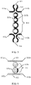
- FIG. 1 is a schematic structural diagram of a first add/drop filter according to an embodiment of this application.
- the add/drop filter includes a first waveguide 101, a second waveguide 102, and a plurality of cascaded ring waveguides 103.
- the first waveguide 101 includes an input port 101a and an output port 101b.
- the second waveguide 102 includes an add port 102a and a drop port 102b.
- the input port 101a and the add port 102a are configured to input an optical signal
- the output port 101b and the drop port 102b are configured to output an optical signal.
- One of the plurality of ring waveguides 103 is coupled to the first waveguide 101, and another of the plurality of ring waveguides 103 is coupled to the second waveguide 102.
- An electrode 103a is disposed on each of the ring waveguides 103.
- a loss adjusting apparatus 103b is disposed on at least one of the ring waveguides except the ring waveguide coupled to
- the ring waveguide coupled to the first waveguide 101 is referred to as a first ring waveguide
- the ring waveguide coupled to the second waveguide 102 is referred to as a second ring waveguide in the following.
- bandwidth of an add/drop filter applied to optical communication needs to reach 40 GHz
- a coupling coefficient between the first ring waveguide and the first waveguide 101 needs to be greater than an in-loop insertion loss of the first ring waveguide.
- the loss adjusting apparatus 103b is also disposed on the first ring waveguide, critical coupling may also occur in a process of increasing the insertion loss in the first ring waveguide.
- the loss adjusting apparatus 103b may be disposed on each of the ring waveguides except the first ring waveguide. As shown in FIG. 1 , the add/drop filter includes four cascaded ring waveguides, and the loss adjusting apparatus 103b is disposed on each of two middle ring waveguides.
- a quantity of the cascaded ring waveguides 103 is not limited in this application, and it is only required that a quantity of the cascaded ring waveguides 103 be not less than 2.
- a quantity of the loss adjusting apparatuss 103b and a location of the loss adjusting apparatus 103b are not limited either, and it is only required that the loss adjusting apparatus 103b be not placed on the first ring waveguide.
- an operating wavelength of the add/drop filter is a resonance wavelength of each of the ring waveguides 103.
- an optical signal of the operating wavelength may be dropped through the drop port 102b, or an optical signal of the operating wavelength may be added through the add port 102a.
- the operating wavelength needs to be reconfigured, normal transmission of signals of wavelengths except that of the operating wavelength from the input port to the output port may be affected. For example, signals of a total of four different wavelengths, ⁇ 1 to ⁇ 4, are input through the input port. If a current operating wavelength is ⁇ 1, the drop port outputs the signal whose wavelength is ⁇ 1, and the output port outputs the signals whose wavelengths are ⁇ 2, ⁇ 3, and ⁇ 4.
- the loss adjusting apparatus 103b may be used to adjust an insertion loss in the at least one ring waveguide. Therefore, an optical signal that enters the ring waveguide is absorbed, and the ring waveguide does not resonate any more, to block the signal transmission between the first waveguide 101 and the second waveguide 102. It may be understood that a larger quantity of loss adjusting apparatuss 103b indicates a better effect of disabling a filtering function.
- FIG. 2 is a schematic diagram of a drop spectrum corresponding to the drop port 102b during normal dropping.
- the loss adjusting apparatus 103b is used to decrease the insertion loss in the ring waveguide corresponding to the loss adjusting apparatus 103b to a minimum value. It can be learned from FIG. 2 that a peak insertion loss of the drop spectrum is approximately 0 dB at this time.
- FIG. 3 is a schematic diagram of a drop spectrum corresponding to the drop port 102b when the filtering function is disabled.
- the loss adjusting apparatus 103b is used to increase the insertion loss in the ring waveguide corresponding to the loss adjusting apparatus 103b to a maximum value. It can be learned from FIG. 3 that, compared with FIG. 2 , a peak change of the drop spectrum exceeds 30 dB at this time, and the filtering function is disabled.
- FIG. 4 is a schematic structural diagram of a second add/drop filter according to an embodiment of this application.
- the add/drop filter may further include a controller 104.
- the loss adjusting apparatus 103b uses an electrical structure that is based on a carrier dispersion effect.
- the controller 104 may change carrier concentration in the ring waveguide by controlling a load voltage of the loss adjusting apparatus 103b, to change the insertion loss in the ring waveguide. In this way, the filtering function is disabled or recovered.
- the loss adjusting apparatus 103b is not limited to the foregoing listed structures.
- a layer of graphene may be added to the ring waveguide, and the graphene layer is used to change the insertion loss in the ring waveguide. This is not specifically limited herein.
- the electrode 103a may be specifically a micro thermal electrode.
- the micro thermal electrode may be disposed on a periphery of each of the ring waveguides 103.
- the micro thermal electrode may be disposed in a same plane with the ring waveguide 103, or the micro thermal electrode may be disposed in a plane different from that of the ring waveguide 103.
- the controller 104 may adjust the resonance wavelength of each of the ring waveguides 103 by controlling a temperature of the micro thermal electrode on each of the ring waveguides 103.
- the ring waveguide 103 may use a material having a thermo-optic effect, for example, a dielectric material (silicon dioxide and silicon nitride) or a semiconductor material (III-V and silicon). Changing of the temperature of the micro thermal electrode may cause changing of a partial temperature of the ring waveguide 103, and a refractive index of the material may be changed based on the thermo-optic effect, to adjust the resonance wavelength of the ring waveguide 103.
- the ring waveguide 103 may alternatively use a material having an electro-optic effect, for example, lithium niobate.
- the controller 104 may alternatively change a refractive index of the material by controlling a voltage on the electrode 103a, to adjust the resonance wavelength of the ring waveguide 103.
- the controller 104 may specifically include a drive of a microcontroller unit (Microcontroller Unit, MCU), the electrode 103a, and the loss adjusting apparatus 103b.
- MCU microcontroller Unit
- FIG. 5 is a schematic structural diagram of a third add/drop filter according to an embodiment of this application.
- a first tunable coupler (Tunable Coupler, TC) 105 is disposed at a position at which the first waveguide 101 is coupled to the first ring waveguide.
- a second tunable coupler 106 is disposed at a position at which the second waveguide 102 is coupled to the second ring waveguide.
- the first waveguide 101 and the second waveguide 102 each include an arc waveguide.
- the arc waveguide on the first waveguide 101 has two coupling points with the first ring waveguide, and the arc waveguide on the second waveguide 102 also has two coupling points with the second ring waveguide.
- Thermal electrodes are disposed on the two arc waveguides.
- the thermal electrodes are controlled to adjust coupling coefficients of the first tunable coupler 105 and the second tunable coupler 106, and therefore bandwidth and in-band isolation of the add/drop filter can be finely adjusted, thereby optimizing performance of the add/drop filter.
- first tunable coupler 105 and the second tunable coupler 106 may be reserved. This is not specifically limited herein.
- the waveguide may alternatively be of a boss shape. This is not specifically limited herein.
- FIG. 6 is a schematic structural diagram of a fourth add/drop filter according to an embodiment of this application. Specifically, an overall structure of the add/drop filter shown in FIG. 6 is similar to that of the add/drop filter shown in FIG. 1 , and same parts are not described herein again. A main difference lies in that the structure of the ring waveguide shown in FIG. 1 is a micro ring, while a structure of a ring waveguide shown in FIG. 6 is a micro disk.
- FIG. 7 is a schematic structural diagram of a fifth add/drop filter according to an embodiment of this application. Specifically, an overall structure of the add/drop filter shown in FIG. 7 is similar to that of the add/drop filter shown in FIG. 1 , and same parts are not described herein again. A main difference lies in that a cascading mode of the plurality of ring waveguides 103 shown in FIG. 1 is serial cascading, while a first ring waveguide shown in FIG. 7 may be coupled to two middle ring waveguides, and a second ring waveguide may also be coupled to two middle ring waveguides.
- the add/drop filter in embodiments of this application includes but is not limited to the foregoing five listed structures, and other variations based on the foregoing structures all fall within the protection scope of this application.
- a plurality of groups of cascaded ring waveguides 103 may be included between the first waveguide 101 and the second waveguide 102.
- Each group of cascaded ring waveguides may use the structure shown in FIG. 1 , or may use the structure shown in FIG. 7 . This is not specifically limited herein.
- a loss adjusting apparatus 103b is disposed on at least one of the ring waveguides 103 except the first ring waveguide, and the loss adjusting apparatus 103b is configured to adjust an insertion loss in the at least one ring waveguide 103.
- the insertion loss in the at least one ring waveguide 103 may be adjusted to block signal transmission between the first waveguide 101 and the second waveguide 102. Because the loss adjusting apparatus 103b is not disposed on the first ring waveguide, in a process of using the loss adjusting apparatus 103b, critical coupling on the first ring waveguide is avoided, thereby ensuring normal transmission of a signal in the first waveguide 101.
- an optical add/drop multiplexer (Optical Add/Drop Multiplexer, OADM) based on the foregoing add/drop filter is further provided.
- the optical add/drop multiplexer may include a plurality of cascaded add/drop filters.
- FIG. 8 is a schematic structural diagram of an optical add/drop multiplexer 20 according to an embodiment of this application.
- the optical add/drop multiplexer 20 is a dual-channel optical add/drop multiplexer, in other words, the optical add/drop multiplexer 20 includes two cascaded add/drop filters, which are a first add/drop filter 21 and a second add/drop filter 22.
- the first add/drop filter 21 includes a first add port 201 and a first drop port 202.
- the second add/drop filter 22 includes a second add port 203 and a second drop port 204.
- the first add/drop filter 21 and the second add/drop filter 22 share a same pair of input port 205 and output port 206.
- the add/drop filter in the optical add/drop multiplexer 20 in this embodiment is similar to the add/drop filter described in the foregoing embodiment. Details are not described herein again.
- FIG. 9 is a schematic flowchart of a wavelength control method based on an add/drop filter according to an embodiment of this application.
- the wavelength control method includes the following steps.
- the add/drop filter in this embodiment may be specifically the add/drop filter in any one of the embodiments shown in FIG. 1 , FIG. 4 , FIG. 5, FIG. 6 , and FIG. 7 .
- FIG. 1 is used as an example in some of the following descriptions.
- the add/drop filter increases a first insertion loss in a target ring waveguide to a second insertion loss, to block signal transmission between a first waveguide and a second waveguide.
- the target ring waveguide is at least one of ring waveguides except a first ring waveguide.
- a loss adjusting apparatus 103b disposed on the target ring waveguide may be used to adjust the insertion loss in the target ring waveguide, so that an optical signal that enters the ring waveguide is absorbed, and the ring waveguide does not resonate any more, to block the signal transmission between the first waveguide 101 and the second waveguide 102.
- the loss adjusting apparatus 103b refer to related descriptions in the foregoing embodiments. Details are not described herein again.
- the add/drop filter adjusts a first resonance wavelength of each of the ring waveguides to a second resonance wavelength.
- the first resonance wavelength of each of the ring waveguides may be adjusted to the second resonance wavelength by controlling a temperature or a voltage of an electrode on each of the ring waveguides. It may be understood that the first resonance wavelength is a current operating wavelength of the add/drop filter, and the second resonance wavelength is a new operating wavelength of the add/drop filter.
- the first resonance wavelength of each of the ring waveguides may be synchronously adjusted to the second resonance wavelength, in other words, resonance wavelengths of different ring waveguides keep synchronous in an adjustment process.
- the ring waveguides may be detuned first, in other words, each of the ring waveguides has a different resonance wavelength, and a resonance condition of the add/drop filter is destroyed. Therefore, all optical signals input through the input port 101a are output through the output port 101b. Then, a resonance wavelength of each of the ring waveguides is adjusted to the second resonance wavelength.
- the add/drop filter recovers the second insertion loss in the target ring waveguide to the first insertion loss, to recover the signal transmission between the first waveguide and the second waveguide.
- the second insertion loss in the target ring waveguide may be recovered to the first insertion loss, so that the signal transmission between the first waveguide 101 and the second waveguide 102 is recovered, and wavelength adding or wavelength dropping can be normally performed on the second waveguide 102.
Landscapes
- Physics & Mathematics (AREA)
- General Physics & Mathematics (AREA)
- Optics & Photonics (AREA)
- Engineering & Computer Science (AREA)
- Computer Networks & Wireless Communication (AREA)
- Signal Processing (AREA)
- Optical Integrated Circuits (AREA)
- Optical Modulation, Optical Deflection, Nonlinear Optics, Optical Demodulation, Optical Logic Elements (AREA)
Abstract
Description
- This application claims priority to
Chinese Patent Application No. 202010018395.3, filed with the China National Intellectual Property Administration on January 8, 2020 - This application relates to the field of optical communication, and in particular, to an add/drop filter, an optical add/drop multiplexer, and a wavelength control method.
- Generally, there are two types of optical add/drop multiplexers (Optical Add/Drop Multiplexers, OADMs) commonly used in the wavelength division field: a space optics OADM and a waveguide OADM. In comparison, the waveguide OADM has advantages of lower costs and higher integration.
- The waveguide OADM includes a plurality of cascaded add/drop filters (Add/Drop Filters, ADFs). The add/drop filter is a key component in an optical fiber dense wavelength division multiplexing system, and can implement wavelength adding and wavelength dropping of a specific wavelength or a specific wavelength combination in a main fiber link. An existing add/drop filter includes a first waveguide, a second waveguide, and a plurality of micro rings between the first waveguide and the second waveguide. The first waveguide includes an input port and an output port, and the second waveguide includes an add port and a drop port. A tunable coupler (Tunable Coupler, TC) is disposed at a position at which the first waveguide is coupled to a first micro ring, and the TC is configured to adjust a coupling coefficient between the first waveguide and the first micro ring. Before an operating wavelength of the add/drop filter is adjusted, the coupling coefficient usually needs to be adjusted to block wavelength adding or wavelength dropping of the second waveguide, and after the operating wavelength is adjusted, the coupling coefficient is adjusted to recover the wavelength adding or the wavelength dropping of the second waveguide.
- Embodiments of this application provide an add/drop filter, an optical add/drop multiplexer, and a wavelength control method.
- According to a first aspect, an embodiment of this application provides an add/drop filter. The filter includes a first waveguide, a second waveguide, and a plurality of cascaded ring waveguides. The first waveguide includes an input port and an output port. The second waveguide includes an add port and a drop port. One of the plurality of cascaded ring waveguides is coupled to the first waveguide, and another of the plurality of cascaded ring waveguides is coupled to the second waveguide. An electrode is disposed on each of the ring waveguides. A loss adjusting apparatus is disposed on at least one of the plurality of cascaded ring waveguides except the one of the plurality of ring waveguides, and the loss adjusting apparatus is configured to adjust an insertion loss in the at least one ring waveguide.
- In this implementation, before an operating wavelength of the add/drop filter is adjusted, the insertion loss in the at least one ring waveguide may be adjusted to block signal transmission between the first waveguide and the second waveguide. Because the loss adjusting apparatus is not disposed on the ring waveguide coupled to the first waveguide, in a process of using the loss adjusting apparatus, critical coupling on the ring waveguide coupled to the first waveguide is avoided, thereby ensuring normal transmission of a signal in the first waveguide.
- In some possible implementations, circumferences of at least two of the plurality of ring waveguides are different. Because ring waveguides with different circumferences correspond to different free spectral ranges (free spectral range, FSR), a plurality of ring waveguides with different radii extend the FSR of the add/drop filter by using a Vernier effect.
- In some possible implementations, the add/drop filter further includes a controller, and the controller is configured to adjust the insertion loss in the at least one ring waveguide by controlling the loss adjusting apparatus on the at least one ring waveguide. In this implementation, a specific implementation of controlling the loss adjusting apparatus is provided, thereby improving practicability of this solution.
- In some possible implementations, the controller is further configured to adjust a resonance wavelength of each of the ring waveguides by controlling a temperature or a voltage of the electrode on each of the ring waveguides. In this implementation, two implementations of adjusting the resonance wavelength of each of the ring waveguides are provided, thereby improving scalability of this solution.
- In some possible implementations, a first tunable coupler (Tunable Coupler, TC) is disposed at a position at which the first waveguide is coupled to the one of the ring waveguides, and a second tunable coupler is disposed at a position at which the second waveguide is coupled to the another of the ring waveguides. Alternatively, only one of the first tunable coupler and the second tunable coupler may be reserved. Coupling coefficients of the first tunable coupler and the second tunable coupler are adjustable, and therefore bandwidth and in-band isolation of the add/drop filter can be finely adjusted, thereby optimizing performance of the add/drop filter.
- In some possible implementations, the ring waveguide is a micro ring or a micro disk, thereby improving flexibility of this solution.
- In some possible implementations, a material of the first waveguide, the second waveguide, and the ring waveguide is silicon, III-V, silicon nitride SiN, or lithium niobate LiNbO3. In this implementation, several waveguide materials are provided, thereby improving implementability of this solution.
- According to a second aspect, an embodiment of this application provides an optical add/drop multiplexer (Optical Add/Drop Multiplexer, OADM). The OADM includes a plurality of the add/drop filters as shown in any one of the implementations of the first aspect that are cascaded.
- According to a third aspect, an embodiment of this application provides a wavelength control method based on an add/drop filter. The method includes the following steps.
- The add/drop filter increases a first insertion loss in a target ring waveguide to a second insertion loss, to block signal transmission between a first waveguide and a second waveguide. The add/drop filter includes the first waveguide, the second waveguide, and a plurality of cascaded ring waveguides, and the target ring waveguide includes at least one of the plurality of cascaded ring waveguides except a first ring waveguide, where the first ring waveguide is a ring waveguide, in the plurality of cascaded ring waveguides, coupled to the first waveguide. Then, the add/drop filter adjusts a first resonance wavelength of each of the ring waveguides to a second resonance wavelength. Further, the add/drop filter recovers the second insertion loss in the target ring waveguide to the first insertion loss, to recover the signal transmission between the first waveguide and the second waveguide.
- In some possible implementations, that the add/drop filter adjusts a first resonance wavelength of each of the ring waveguides to a second resonance wavelength includes the following steps.
- The add/drop filter adjusts the first resonance wavelength of each of the ring waveguides to the second resonance wavelength by controlling a temperature or a voltage of an electrode on each of the ring waveguides. In this implementation, a specific implementation of adjusting the resonance wavelength of the ring waveguide is provided, thereby improving practicability of this solution.
- In some possible implementations, that the add/drop filter adjusts a first resonance wavelength of each of the ring waveguides to a second resonance wavelength includes the following steps.
- The add/drop filter adjusts the first resonance wavelength of each of the ring waveguides, so that the plurality of the ring waveguides are detuned, in other words, each of the ring waveguides has a different resonance wavelength. A resonant condition of the add/drop filter is destroyed, and therefore all optical signals input through an input port are output through an output port. Then, a resonance wavelength of each of the ring waveguides is adjusted to the second resonance wavelength. The signal transmission between the first waveguide and the second waveguide is further blocked, to increase a blocking effect.
- It can be learnt from the foregoing technical solutions that embodiments of this application have the following advantages: Because the loss adjusting apparatus is not disposed on the ring waveguide coupled to the first waveguide, in a process of using the loss adjusting apparatus, critical coupling on the ring waveguide coupled to the first waveguide is avoided, thereby ensuring normal transmission of a signal in the first waveguide.
-
-
FIG. 1 is a schematic structural diagram of a first add/drop filter according to an embodiment of this application; -
FIG. 2 is a schematic diagram of a drop spectrum corresponding to a drop port during normal dropping; -
FIG. 3 is a schematic diagram of a drop spectrum corresponding to a drop port when a filtering function is disabled; -
FIG. 4 is a schematic structural diagram of a second add/drop filter according to an embodiment of this application; -
FIG. 5 is a schematic structural diagram of a third add/drop filter according to an embodiment of this application; -
FIG. 6 is a schematic structural diagram of a fourth add/drop filter according to an embodiment of this application; -
FIG. 7 is a schematic structural diagram of a fifth add/drop filter according to an embodiment of this application; -
FIG. 8 is a schematic structural diagram of an optical add/drop multiplexer according to an embodiment of this application; and -
FIG. 9 is a schematic flowchart of a wavelength control method based on an add/drop filter according to an embodiment of this application. - Embodiments of this application provide an add/drop filter, an optical add/drop multiplexer, and a wavelength control method. Because a loss adjusting apparatus is not disposed on a ring waveguide coupled to a first waveguide, in a process of using the loss adjusting apparatus, critical coupling on the ring waveguide coupled to the first waveguide is avoided, thereby ensuring normal transmission of a signal in the first waveguide.
- It should be noted that the terms "first", "second", "third", "fourth", and the like in the specification, claims, and accompanying drawings of this application are used to distinguish between similar objects, but do not limit a specific order or sequence. It should be understood that the foregoing terms are interchangeable in proper circumstances, so that embodiments described in this application can be implemented in other orders rather than the content described in this application. Moreover, the terms "include", "have", or any other variant thereof are intended to cover non-exclusive inclusion. For example, processes, methods, systems, products, or devices that include a series of steps or units are not limited to the steps or the units that are clearly listed, and may include other steps and units that are not clearly listed or that are essential for the processes, methods, products, or devices.
- An existing add/drop filter includes a first waveguide, a second waveguide, and a plurality of micro rings between the first waveguide and the second waveguide. A tunable coupler is disposed at a position at which the first waveguide is coupled to a first micro ring, and is configured to adjust a coupling coefficient between the first waveguide and the first micro ring. It is found through research that, in a changing process of the coupling coefficient, critical coupling may occur on the first micro ring coupled to the first waveguide at a specific moment. Consequently, a phase response of a pass-through spectrum corresponding to an output port in the first waveguide is distorted at the moment, affecting normal transmission of a signal in the first waveguide.
- Therefore, an embodiment of this application provides an add/drop filter, to ensure the normal transmission of the signal in the first waveguide.
-
FIG. 1 is a schematic structural diagram of a first add/drop filter according to an embodiment of this application. The add/drop filter includes afirst waveguide 101, asecond waveguide 102, and a plurality of cascadedring waveguides 103. Thefirst waveguide 101 includes aninput port 101a and anoutput port 101b. Thesecond waveguide 102 includes anadd port 102a and adrop port 102b. Theinput port 101a and theadd port 102a are configured to input an optical signal, and theoutput port 101b and thedrop port 102b are configured to output an optical signal. One of the plurality ofring waveguides 103 is coupled to thefirst waveguide 101, and another of the plurality ofring waveguides 103 is coupled to thesecond waveguide 102. Anelectrode 103a is disposed on each of thering waveguides 103. Aloss adjusting apparatus 103b is disposed on at least one of the ring waveguides except the ring waveguide coupled to thefirst waveguide 101. - For ease of description, the ring waveguide coupled to the
first waveguide 101 is referred to as a first ring waveguide, and the ring waveguide coupled to thesecond waveguide 102 is referred to as a second ring waveguide in the following. It should be noted that, bandwidth of an add/drop filter applied to optical communication needs to reach 40 GHz, and a coupling coefficient between the first ring waveguide and thefirst waveguide 101 needs to be greater than an in-loop insertion loss of the first ring waveguide. If theloss adjusting apparatus 103b is also disposed on the first ring waveguide, critical coupling may also occur in a process of increasing the insertion loss in the first ring waveguide. Such critical coupling distorts an amplitude response and a phase response of a corresponding frequency of a pass-through spectrum corresponding to theoutput port 101b in thefirst waveguide 101, affecting normal transmission of a signal in thefirst waveguide 101. For the ring waveguides except the first ring waveguide, critical coupling caused by increasing the insertion loss does not occur. Therefore, theloss adjusting apparatus 103b may be disposed on each of the ring waveguides except the first ring waveguide. As shown inFIG. 1 , the add/drop filter includes four cascaded ring waveguides, and theloss adjusting apparatus 103b is disposed on each of two middle ring waveguides. - It should be noted that, a quantity of the cascaded
ring waveguides 103 is not limited in this application, and it is only required that a quantity of the cascadedring waveguides 103 be not less than 2. In addition, a quantity of theloss adjusting apparatuss 103b and a location of theloss adjusting apparatus 103b are not limited either, and it is only required that theloss adjusting apparatus 103b be not placed on the first ring waveguide. - In this embodiment of this application, an operating wavelength of the add/drop filter is a resonance wavelength of each of the
ring waveguides 103. In other words, an optical signal of the operating wavelength may be dropped through thedrop port 102b, or an optical signal of the operating wavelength may be added through theadd port 102a. When the operating wavelength needs to be reconfigured, normal transmission of signals of wavelengths except that of the operating wavelength from the input port to the output port may be affected. For example, signals of a total of four different wavelengths, λ1 to λ4, are input through the input port. If a current operating wavelength is λ1, the drop port outputs the signal whose wavelength is λ1, and the output port outputs the signals whose wavelengths are λ2, λ3, and λ4. In a process of adjusting the operating wavelength from λ1 to λ4 by using the conventional technology, moments at which operating wavelengths are λ2 and λ3 may occur, affecting normal transmission of the signals whose wavelengths are λ2 and λ3. Therefore, signal transmission between thefirst waveguide 101 and thesecond waveguide 102 needs to be blocked before the operating wavelength is switched, in other words, all optical signals input through theinput port 101a are output through theoutput port 101b. Then, after the operating wavelength is switched, the signal transmission between thefirst waveguide 101 and thesecond waveguide 102 is recovered. - Specifically, the
loss adjusting apparatus 103b may be used to adjust an insertion loss in the at least one ring waveguide. Therefore, an optical signal that enters the ring waveguide is absorbed, and the ring waveguide does not resonate any more, to block the signal transmission between thefirst waveguide 101 and thesecond waveguide 102. It may be understood that a larger quantity ofloss adjusting apparatuss 103b indicates a better effect of disabling a filtering function. - With reference to more accompanying drawings, the following further describes a process of disabling the filtering function by the add/drop filter.
-
FIG. 2 is a schematic diagram of a drop spectrum corresponding to thedrop port 102b during normal dropping. To enable an optical signal of an operating wavelength to be normally dropped through thedrop port 102b, theloss adjusting apparatus 103b is used to decrease the insertion loss in the ring waveguide corresponding to theloss adjusting apparatus 103b to a minimum value. It can be learned fromFIG. 2 that a peak insertion loss of the drop spectrum is approximately 0 dB at this time. -
FIG. 3 is a schematic diagram of a drop spectrum corresponding to thedrop port 102b when the filtering function is disabled. To disable the filtering function, theloss adjusting apparatus 103b is used to increase the insertion loss in the ring waveguide corresponding to theloss adjusting apparatus 103b to a maximum value. It can be learned fromFIG. 3 that, compared withFIG. 2 , a peak change of the drop spectrum exceeds 30 dB at this time, and the filtering function is disabled. -
FIG. 4 is a schematic structural diagram of a second add/drop filter according to an embodiment of this application. In some embodiments of this application, the add/drop filter may further include acontroller 104. Theloss adjusting apparatus 103b uses an electrical structure that is based on a carrier dispersion effect. Thecontroller 104 may change carrier concentration in the ring waveguide by controlling a load voltage of theloss adjusting apparatus 103b, to change the insertion loss in the ring waveguide. In this way, the filtering function is disabled or recovered. It should be noted that theloss adjusting apparatus 103b is not limited to the foregoing listed structures. For example, a layer of graphene may be added to the ring waveguide, and the graphene layer is used to change the insertion loss in the ring waveguide. This is not specifically limited herein. - In some embodiments of this application, the
electrode 103a may be specifically a micro thermal electrode. The micro thermal electrode may be disposed on a periphery of each of thering waveguides 103. For example, the micro thermal electrode may be disposed in a same plane with thering waveguide 103, or the micro thermal electrode may be disposed in a plane different from that of thering waveguide 103. Thecontroller 104 may adjust the resonance wavelength of each of thering waveguides 103 by controlling a temperature of the micro thermal electrode on each of thering waveguides 103. Specifically, thering waveguide 103 may use a material having a thermo-optic effect, for example, a dielectric material (silicon dioxide and silicon nitride) or a semiconductor material (III-V and silicon). Changing of the temperature of the micro thermal electrode may cause changing of a partial temperature of thering waveguide 103, and a refractive index of the material may be changed based on the thermo-optic effect, to adjust the resonance wavelength of thering waveguide 103. In addition, thering waveguide 103 may alternatively use a material having an electro-optic effect, for example, lithium niobate. Thecontroller 104 may alternatively change a refractive index of the material by controlling a voltage on theelectrode 103a, to adjust the resonance wavelength of thering waveguide 103. - It may be understood that, when the resonance wavelengths of all the
ring waveguides 103 are the same, the resonance wavelength is an operating wavelength of the add/drop filter. Thecontroller 104 may specifically include a drive of a microcontroller unit (Microcontroller Unit, MCU), theelectrode 103a, and theloss adjusting apparatus 103b. - Optionally, circumferences of at least two of the plurality of
ring waveguides 103 are different. Ring waveguides with different circumferences correspond to different free spectral ranges (free spectral ranges, FSRs). Specifically, FSR=λ2/L∗neff. λ represents the resonance wavelength of thering waveguide 103, L represents the circumference of thering waveguide 103, and neff represents an effective refractive index of thering waveguide 103. Therefore, a plurality ofring waveguides 103 with different radii extend an FSR of the add/drop filter based on a vernier effect. It may be understood that, if a structure of thering waveguide 103 is a micro ring, at least two of the plurality of micro rings have different radii. -
FIG. 5 is a schematic structural diagram of a third add/drop filter according to an embodiment of this application. In some embodiments of this application, a first tunable coupler (Tunable Coupler, TC) 105 is disposed at a position at which thefirst waveguide 101 is coupled to the first ring waveguide. A secondtunable coupler 106 is disposed at a position at which thesecond waveguide 102 is coupled to the second ring waveguide. Specifically, as shown inFIG. 5 , thefirst waveguide 101 and thesecond waveguide 102 each include an arc waveguide. The arc waveguide on thefirst waveguide 101 has two coupling points with the first ring waveguide, and the arc waveguide on thesecond waveguide 102 also has two coupling points with the second ring waveguide. Thermal electrodes are disposed on the two arc waveguides. The thermal electrodes are controlled to adjust coupling coefficients of the firsttunable coupler 105 and the secondtunable coupler 106, and therefore bandwidth and in-band isolation of the add/drop filter can be finely adjusted, thereby optimizing performance of the add/drop filter. - Optionally, only one of the first
tunable coupler 105 and the secondtunable coupler 106 may be reserved. This is not specifically limited herein. In addition, in addition to the foregoing listed arc waveguide, there may further be a waveguide of another shape between two coupling points of thefirst waveguide 101 and the first ring waveguide. For example, the waveguide may alternatively be of a boss shape. This is not specifically limited herein. -
FIG. 6 is a schematic structural diagram of a fourth add/drop filter according to an embodiment of this application. Specifically, an overall structure of the add/drop filter shown inFIG. 6 is similar to that of the add/drop filter shown inFIG. 1 , and same parts are not described herein again. A main difference lies in that the structure of the ring waveguide shown inFIG. 1 is a micro ring, while a structure of a ring waveguide shown inFIG. 6 is a micro disk. -
FIG. 7 is a schematic structural diagram of a fifth add/drop filter according to an embodiment of this application. Specifically, an overall structure of the add/drop filter shown inFIG. 7 is similar to that of the add/drop filter shown inFIG. 1 , and same parts are not described herein again. A main difference lies in that a cascading mode of the plurality ofring waveguides 103 shown inFIG. 1 is serial cascading, while a first ring waveguide shown inFIG. 7 may be coupled to two middle ring waveguides, and a second ring waveguide may also be coupled to two middle ring waveguides. In this case, there may be a plurality of paths for signal transmission between thefirst waveguide 101 and thesecond waveguide 102, thereby improving scalability of this solution. This application includes but is not limited to the foregoing listed cascading modes of the ring waveguides. - It should be noted that the add/drop filter in embodiments of this application includes but is not limited to the foregoing five listed structures, and other variations based on the foregoing structures all fall within the protection scope of this application. For example, a plurality of groups of cascaded
ring waveguides 103 may be included between thefirst waveguide 101 and thesecond waveguide 102. Each group of cascaded ring waveguides may use the structure shown inFIG. 1 , or may use the structure shown inFIG. 7 . This is not specifically limited herein. - In this embodiment of this application, a
loss adjusting apparatus 103b is disposed on at least one of thering waveguides 103 except the first ring waveguide, and theloss adjusting apparatus 103b is configured to adjust an insertion loss in the at least onering waveguide 103. Before an operating wavelength of the add/drop filter is adjusted, the insertion loss in the at least onering waveguide 103 may be adjusted to block signal transmission between thefirst waveguide 101 and thesecond waveguide 102. Because theloss adjusting apparatus 103b is not disposed on the first ring waveguide, in a process of using theloss adjusting apparatus 103b, critical coupling on the first ring waveguide is avoided, thereby ensuring normal transmission of a signal in thefirst waveguide 101. - In some embodiments of this application, an optical add/drop multiplexer (Optical Add/Drop Multiplexer, OADM) based on the foregoing add/drop filter is further provided. The optical add/drop multiplexer may include a plurality of cascaded add/drop filters.
-
FIG. 8 is a schematic structural diagram of an optical add/drop multiplexer 20 according to an embodiment of this application. The optical add/drop multiplexer 20 is a dual-channel optical add/drop multiplexer, in other words, the optical add/drop multiplexer 20 includes two cascaded add/drop filters, which are a first add/drop filter 21 and a second add/drop filter 22. The first add/drop filter 21 includes afirst add port 201 and afirst drop port 202. The second add/drop filter 22 includes asecond add port 203 and asecond drop port 204. In addition, the first add/drop filter 21 and the second add/drop filter 22 share a same pair ofinput port 205 andoutput port 206. Specifically, the add/drop filter in the optical add/drop multiplexer 20 in this embodiment is similar to the add/drop filter described in the foregoing embodiment. Details are not described herein again. - Based on the foregoing description of the add/drop filter, the following describes a wavelength control method corresponding to the add/drop filter. It should be noted that, descriptions of an apparatus structure corresponding to the following wavelength control method may be the same as the descriptions in the foregoing apparatus embodiment. However, this is not limited to the add/drop filter described above.
-
FIG. 9 is a schematic flowchart of a wavelength control method based on an add/drop filter according to an embodiment of this application. In this example, the wavelength control method includes the following steps. - It should be noted that, the add/drop filter in this embodiment may be specifically the add/drop filter in any one of the embodiments shown in
FIG. 1 ,FIG. 4 ,FIG. 5, FIG. 6 , andFIG. 7 . For brief description,FIG. 1 is used as an example in some of the following descriptions. - 901. The add/drop filter increases a first insertion loss in a target ring waveguide to a second insertion loss, to block signal transmission between a first waveguide and a second waveguide.
- In this embodiment, the target ring waveguide is at least one of ring waveguides except a first ring waveguide. Specifically, a
loss adjusting apparatus 103b disposed on the target ring waveguide may be used to adjust the insertion loss in the target ring waveguide, so that an optical signal that enters the ring waveguide is absorbed, and the ring waveguide does not resonate any more, to block the signal transmission between thefirst waveguide 101 and thesecond waveguide 102. For descriptions of theloss adjusting apparatus 103b, refer to related descriptions in the foregoing embodiments. Details are not described herein again. - 902. The add/drop filter adjusts a first resonance wavelength of each of the ring waveguides to a second resonance wavelength.
- In this embodiment, after the signal transmission between the
first waveguide 101 and thesecond waveguide 102 is blocked, all optical signals input through theinput port 101a are output through theoutput port 101b. Therefore, adjustment of an operating wavelength of the add/drop filter does not affect normal transmission of a signal in thefirst waveguide 101. Specifically, the first resonance wavelength of each of the ring waveguides may be adjusted to the second resonance wavelength by controlling a temperature or a voltage of an electrode on each of the ring waveguides. It may be understood that the first resonance wavelength is a current operating wavelength of the add/drop filter, and the second resonance wavelength is a new operating wavelength of the add/drop filter. - It should be noted that the first resonance wavelength of each of the ring waveguides may be synchronously adjusted to the second resonance wavelength, in other words, resonance wavelengths of different ring waveguides keep synchronous in an adjustment process.
- Optionally, to further block the signal transmission between the
first waveguide 101 and thesecond waveguide 102 to improve a blocking effect, the ring waveguides may be detuned first, in other words, each of the ring waveguides has a different resonance wavelength, and a resonance condition of the add/drop filter is destroyed. Therefore, all optical signals input through theinput port 101a are output through theoutput port 101b. Then, a resonance wavelength of each of the ring waveguides is adjusted to the second resonance wavelength. - 903. The add/drop filter recovers the second insertion loss in the target ring waveguide to the first insertion loss, to recover the signal transmission between the first waveguide and the second waveguide.
- In this embodiment, after the operating wavelength of the add/drop filter is switched, the second insertion loss in the target ring waveguide may be recovered to the first insertion loss, so that the signal transmission between the
first waveguide 101 and thesecond waveguide 102 is recovered, and wavelength adding or wavelength dropping can be normally performed on thesecond waveguide 102. - It should be noted that the foregoing embodiments are merely used to describe the technical solutions of this application, but are not intended to limit this application. Although this application is described in detail with reference to the foregoing embodiments, persons of ordinary skill in the art should understand that they may still make modifications to the technical solutions described in the foregoing embodiments or make equivalent replacements to some technical features thereof, without departing from the scope of the technical solutions of embodiments of this application.
Claims (11)
- An add/drop filter, comprising: a first waveguide, a second waveguide, and a plurality of cascaded ring waveguides, wherein the first waveguide comprises an input port and an output port; the second waveguide comprises an add port and a drop port; one of the plurality of cascaded ring waveguides is coupled to the first waveguide, and another of the plurality of cascaded ring waveguides is coupled to the second waveguide; an electrode is disposed on each of the ring waveguides; and a loss adjusting apparatus is disposed on at least one of the plurality of cascaded ring waveguides except the one of the plurality of ring waveguides, and the loss adjusting apparatus is configured to adjust an insertion loss in the at least one ring waveguide.
- The add/drop filter according to claim 1, wherein circumferences of at least two of the plurality of ring waveguides are different.
- The add/drop filter according to claim 1 or 2, wherein the add/drop filter further comprises a controller, and the controller is configured to adjust the insertion loss in the at least one ring waveguide by controlling the loss adjusting apparatus on the at least one ring waveguide.
- The add/drop filter according to claim 3, wherein the controller is further configured to adjust a resonance wavelength of each of the ring waveguides by controlling a temperature or a voltage of the electrode on each of the ring waveguides.
- The add/drop filter according to any one of claims 1 to 4, wherein a first tunable coupler, TC, is disposed at a position at which the first waveguide is coupled to the one of the ring waveguides, and/or a second TC is disposed at a position at which the second waveguide is coupled to the another of the ring waveguides.
- The add/drop filter according to any one of claims 1 to 5, wherein each of the ring waveguides is a micro ring or a micro disk.
- The add/drop filter according to any one of claims 1 to 5, wherein a material of the first waveguide, the second waveguide, and the ring waveguide is silicon, III-V, silicon nitride, SiN, or lithium niobate, LiNbO3.
- An optical add/drop multiplexer, comprising a plurality of the add/drop filters according to any one of claims 1 to 7 that are cascaded.
- A wavelength control method based on an add/drop filter, wherein the method comprises:increasing, by the add/drop filter, a first insertion loss in a target ring waveguide to a second insertion loss, to block signal transmission between a first waveguide and a second waveguide, wherein the add/drop filter comprises the first waveguide, the second waveguide, and a plurality of cascaded ring waveguides; the target ring waveguide comprises at least one of the plurality of cascaded ring waveguides except a first ring waveguide; and the first ring waveguide is a ring waveguide, in the plurality of cascaded ring waveguides, coupled to the first waveguide;adjusting, by the add/drop filter, a first resonance wavelength of each of the ring waveguides to a second resonance wavelength; andrecovering, by the add/drop filter, the second insertion loss in the target ring waveguide to the first insertion loss, to recover the signal transmission between the first waveguide and the second waveguide.
- The method according to claim 9, wherein the adjusting, by the add/drop filter, a first resonance wavelength of each of the ring waveguides to a second resonance wavelength comprises:
adjusting, by the add/drop filter, the first resonance wavelength of each of the ring waveguides to the second resonance wavelength by controlling a temperature or a voltage of an electrode on each of the ring waveguides. - The method according to claim 9, wherein the adjusting, by the add/drop filter, a first resonance wavelength of each of the ring waveguides to a second resonance wavelength comprises:adjusting, by the add/drop filter, the first resonance wavelength of each of the ring waveguides, to detune the plurality of the ring waveguides; andadjusting, by the add/drop filter, a resonance wavelength of each of the ring waveguides to the second resonance wavelength.
Applications Claiming Priority (2)
| Application Number | Priority Date | Filing Date | Title |
|---|---|---|---|
| CN202010018395.3A CN113093338B (en) | 2020-01-08 | 2020-01-08 | An upload and download filter, optical add-drop multiplexer and wavelength control method |
| PCT/CN2020/141355 WO2021139580A1 (en) | 2020-01-08 | 2020-12-30 | Add/drop filter, optical add/drop multiplexer and wavelength control method |
Publications (3)
| Publication Number | Publication Date |
|---|---|
| EP4080797A1 true EP4080797A1 (en) | 2022-10-26 |
| EP4080797A4 EP4080797A4 (en) | 2023-06-28 |
| EP4080797B1 EP4080797B1 (en) | 2025-05-21 |
Family
ID=76663301
Family Applications (1)
| Application Number | Title | Priority Date | Filing Date |
|---|---|---|---|
| EP20912214.2A Active EP4080797B1 (en) | 2020-01-08 | 2020-12-30 | Add/drop filter, optical add/drop multiplexer and wavelength control method |
Country Status (3)
| Country | Link |
|---|---|
| EP (1) | EP4080797B1 (en) |
| CN (1) | CN113093338B (en) |
| WO (1) | WO2021139580A1 (en) |
Family Cites Families (22)
| Publication number | Priority date | Publication date | Assignee | Title |
|---|---|---|---|---|
| US7106917B2 (en) * | 1998-11-13 | 2006-09-12 | Xponent Photonics Inc | Resonant optical modulators |
| US6928209B2 (en) * | 2003-02-15 | 2005-08-09 | Intel Corporation | Optical add and drop multiplexer using ring resonators |
| WO2005010582A1 (en) * | 2003-07-15 | 2005-02-03 | Massachusetts Institute Of Technology | Optical coupled-resonator filters with asymmetric coupling |
| TWI251393B (en) * | 2004-03-31 | 2006-03-11 | Nec Corp | Tunable laser |
| WO2008118465A2 (en) * | 2007-03-26 | 2008-10-02 | Massachusetts Institute Of Technology | Hitless tuning and switching of optical resonator amplitude and phase responses |
| CN101403811B (en) * | 2008-10-10 | 2010-04-14 | 东南大学 | Surface Plasmon Tunable Optical Resonant Ring Filters |
| CN101696934B (en) * | 2009-10-26 | 2011-01-05 | 浙江大学 | A Cascaded Ring Cavity Optical Waveguide Sensor Based on Vernier Effect |
| US8606055B2 (en) * | 2009-11-06 | 2013-12-10 | Cornell University | Pin diode tuned multiple ring waveguide resonant optical cavity switch and method |
| CN101813805B (en) * | 2010-03-31 | 2012-01-04 | 中国科学院半导体研究所 | Double-ring resonance four-path reconfigurable optical add-drop multiplexer structure |
| CN101840028A (en) * | 2010-04-07 | 2010-09-22 | 中国科学院半导体研究所 | Integrated reconfigurable optical add/drop multiplexer based on microring resonator |
| CN101840029B (en) * | 2010-04-28 | 2012-07-11 | 中国科学院半导体研究所 | An Integrated Reconfigurable Optical Add-Drop Multiplexer |
| US9223086B2 (en) * | 2011-01-21 | 2015-12-29 | Hewlett Packard Enterprise Development Lp | Wavefront synthesizer systems |
| US10447409B2 (en) * | 2013-06-21 | 2019-10-15 | Northrop Grumman Systems Corporation | Optical channelizer for W-band detection |
| CN103995318B (en) * | 2014-04-22 | 2016-08-17 | 暨南大学 | Optically download wave filter that micro-nano fiber ring couples with side-polished fiber and preparation method thereof |
| CN104317068A (en) * | 2014-10-29 | 2015-01-28 | 中国科学院半导体研究所 | Integrated optical filter with center wavelength and filter bandwidth both adjustable independently |
| CN105259614A (en) * | 2015-11-20 | 2016-01-20 | 大连民族大学 | Band pass box-type filter based on ring resonator structure |
| US20170187483A1 (en) * | 2015-12-29 | 2017-06-29 | Huawei Technologies Co., Ltd. | Low transit loss add-drop multiplexing node for all optical networking |
| CN106788864B (en) * | 2016-11-28 | 2018-06-19 | 广西大学 | A kind of integrated reconfigurable optical add-drop multiplexer |
| CN108802907B (en) * | 2017-04-26 | 2020-03-10 | 华为技术有限公司 | A Reconfigurable Optical Add-Drop Multiplexer |
| CN109802743B (en) * | 2017-11-17 | 2020-08-07 | 海思光电子有限公司 | An upload and download filter and optical add-drop multiplexer |
| CN110161629B (en) * | 2019-04-17 | 2021-03-30 | 中山大学 | Integrated adjustable light delay line based on micro-ring array and preparation method thereof |
| CN110095842B (en) * | 2019-04-18 | 2020-06-30 | 东北林业大学 | Full light intensity modulator based on double ring-shaped resonant cavity |
-
2020
- 2020-01-08 CN CN202010018395.3A patent/CN113093338B/en active Active
- 2020-12-30 WO PCT/CN2020/141355 patent/WO2021139580A1/en not_active Ceased
- 2020-12-30 EP EP20912214.2A patent/EP4080797B1/en active Active
Also Published As
| Publication number | Publication date |
|---|---|
| CN113093338A (en) | 2021-07-09 |
| EP4080797A4 (en) | 2023-06-28 |
| WO2021139580A1 (en) | 2021-07-15 |
| EP4080797B1 (en) | 2025-05-21 |
| CN113093338B (en) | 2022-12-13 |
Similar Documents
| Publication | Publication Date | Title |
|---|---|---|
| EP3703287B1 (en) | Upload and download filter and optical add-drop multiplexer | |
| CN107959541B (en) | The control method and device of micro-ring resonator | |
| EP3952151B1 (en) | Optical add-drop multiplexing apparatus and method for controlling same | |
| CN107870397B (en) | Wavelength Selective Optical Switch | |
| CN105549157A (en) | Tunable optical notching filter based on microring resonators | |
| EP4080797B1 (en) | Add/drop filter, optical add/drop multiplexer and wavelength control method | |
| CN113031162A (en) | Optical filter | |
| CN110945807B (en) | Optical add-drop multiplexer and optical signal transmission method | |
| Milanizadeh et al. | FSR-free filter with hitless tunability across C+ L telecom band | |
| Hossein-Zadeh et al. | Importance of intrinsic-$ Q $ in microring-based optical filters and dispersion-compensation devices | |
| Petrini et al. | Reconfigurable FSR-free microring resonator filter with wide hitless tunability | |
| Little et al. | Tunable bandwidth microring resonator filters | |
| CN113504610B (en) | High roll-off optical filter | |
| Kato et al. | Bessel–Thompson filter using double-series-coupled microring resonator | |
| Jiang et al. | Quantitative dispersion model for self-dispersion compensation and parameter optimization of interleavers | |
| Dong et al. | A tunable optical channelizing filter using silicon coupled ring resonators | |
| Milanizadeh et al. | Polarization insensitive tunable hitless filter for extended c band | |
| Chen | Dispersion-compensating optical digital filters for 40-Gb/s metro add-drop applications | |
| CN113534299B (en) | Multichannel non-periodic photonic crystal structure based on optical fractal | |
| Van et al. | Micro-ring resonator filters | |
| Popovic et al. | General approach to hitless switching and FSR extension resonators in integrated photonic circuits | |
| Shen et al. | Reconfigurable silicon optical filters using a dual-ring assisted Mach-Zehnder interferometer based 16× 16 switch | |
| ABDERRAHMANE¹ et al. | A DESIGN FOR A TUNABLE HYBRID SOLC FILTER FOR 40 GBPS DWDM OPTICAL SYSTEMS | |
| Yao et al. | Bandwidth-Tunable Add-Drop Filters Based on MEMS-Actuated Single-Crystalline Silicon Microtoroidal Resonators | |
| US20120257130A1 (en) | Tunable Wavelength Filter |
Legal Events
| Date | Code | Title | Description |
|---|---|---|---|
| STAA | Information on the status of an ep patent application or granted ep patent |
Free format text: STATUS: THE INTERNATIONAL PUBLICATION HAS BEEN MADE |
|
| PUAI | Public reference made under article 153(3) epc to a published international application that has entered the european phase |
Free format text: ORIGINAL CODE: 0009012 |
|
| STAA | Information on the status of an ep patent application or granted ep patent |
Free format text: STATUS: REQUEST FOR EXAMINATION WAS MADE |
|
| 17P | Request for examination filed |
Effective date: 20220719 |
|
| AK | Designated contracting states |
Kind code of ref document: A1 Designated state(s): AL AT BE BG CH CY CZ DE DK EE ES FI FR GB GR HR HU IE IS IT LI LT LU LV MC MK MT NL NO PL PT RO RS SE SI SK SM TR |
|
| DAV | Request for validation of the european patent (deleted) | ||
| DAX | Request for extension of the european patent (deleted) | ||
| A4 | Supplementary search report drawn up and despatched |
Effective date: 20230526 |
|
| RIC1 | Information provided on ipc code assigned before grant |
Ipc: G02B 6/293 20060101ALI20230522BHEP Ipc: H04J 14/02 20060101AFI20230522BHEP |
|
| GRAP | Despatch of communication of intention to grant a patent |
Free format text: ORIGINAL CODE: EPIDOSNIGR1 |
|
| STAA | Information on the status of an ep patent application or granted ep patent |
Free format text: STATUS: GRANT OF PATENT IS INTENDED |
|
| INTG | Intention to grant announced |
Effective date: 20250131 |
|
| GRAS | Grant fee paid |
Free format text: ORIGINAL CODE: EPIDOSNIGR3 |
|
| GRAA | (expected) grant |
Free format text: ORIGINAL CODE: 0009210 |
|
| STAA | Information on the status of an ep patent application or granted ep patent |
Free format text: STATUS: THE PATENT HAS BEEN GRANTED |
|
| AK | Designated contracting states |
Kind code of ref document: B1 Designated state(s): AL AT BE BG CH CY CZ DE DK EE ES FI FR GB GR HR HU IE IS IT LI LT LU LV MC MK MT NL NO PL PT RO RS SE SI SK SM TR |
|
| REG | Reference to a national code |
Ref country code: GB Ref legal event code: FG4D |
|
| REG | Reference to a national code |
Ref country code: CH Ref legal event code: EP |
|
| REG | Reference to a national code |
Ref country code: DE Ref legal event code: R096 Ref document number: 602020051878 Country of ref document: DE |
|
| REG | Reference to a national code |
Ref country code: IE Ref legal event code: FG4D |
|
| REG | Reference to a national code |
Ref country code: NL Ref legal event code: MP Effective date: 20250521 |
|
| PG25 | Lapsed in a contracting state [announced via postgrant information from national office to epo] |
Ref country code: FI Free format text: LAPSE BECAUSE OF FAILURE TO SUBMIT A TRANSLATION OF THE DESCRIPTION OR TO PAY THE FEE WITHIN THE PRESCRIBED TIME-LIMIT Effective date: 20250521 Ref country code: ES Free format text: LAPSE BECAUSE OF FAILURE TO SUBMIT A TRANSLATION OF THE DESCRIPTION OR TO PAY THE FEE WITHIN THE PRESCRIBED TIME-LIMIT Effective date: 20250521 Ref country code: PT Free format text: LAPSE BECAUSE OF FAILURE TO SUBMIT A TRANSLATION OF THE DESCRIPTION OR TO PAY THE FEE WITHIN THE PRESCRIBED TIME-LIMIT Effective date: 20250922 |
|
| REG | Reference to a national code |
Ref country code: LT Ref legal event code: MG9D |
|
| PG25 | Lapsed in a contracting state [announced via postgrant information from national office to epo] |
Ref country code: NO Free format text: LAPSE BECAUSE OF FAILURE TO SUBMIT A TRANSLATION OF THE DESCRIPTION OR TO PAY THE FEE WITHIN THE PRESCRIBED TIME-LIMIT Effective date: 20250821 Ref country code: GR Free format text: LAPSE BECAUSE OF FAILURE TO SUBMIT A TRANSLATION OF THE DESCRIPTION OR TO PAY THE FEE WITHIN THE PRESCRIBED TIME-LIMIT Effective date: 20250822 |
|
| PG25 | Lapsed in a contracting state [announced via postgrant information from national office to epo] |
Ref country code: PL Free format text: LAPSE BECAUSE OF FAILURE TO SUBMIT A TRANSLATION OF THE DESCRIPTION OR TO PAY THE FEE WITHIN THE PRESCRIBED TIME-LIMIT Effective date: 20250521 Ref country code: NL Free format text: LAPSE BECAUSE OF FAILURE TO SUBMIT A TRANSLATION OF THE DESCRIPTION OR TO PAY THE FEE WITHIN THE PRESCRIBED TIME-LIMIT Effective date: 20250521 |
|
| PG25 | Lapsed in a contracting state [announced via postgrant information from national office to epo] |
Ref country code: BG Free format text: LAPSE BECAUSE OF FAILURE TO SUBMIT A TRANSLATION OF THE DESCRIPTION OR TO PAY THE FEE WITHIN THE PRESCRIBED TIME-LIMIT Effective date: 20250521 |
|
| PG25 | Lapsed in a contracting state [announced via postgrant information from national office to epo] |
Ref country code: HR Free format text: LAPSE BECAUSE OF FAILURE TO SUBMIT A TRANSLATION OF THE DESCRIPTION OR TO PAY THE FEE WITHIN THE PRESCRIBED TIME-LIMIT Effective date: 20250521 |
|
| PG25 | Lapsed in a contracting state [announced via postgrant information from national office to epo] |
Ref country code: RS Free format text: LAPSE BECAUSE OF FAILURE TO SUBMIT A TRANSLATION OF THE DESCRIPTION OR TO PAY THE FEE WITHIN THE PRESCRIBED TIME-LIMIT Effective date: 20250821 |
|
| PG25 | Lapsed in a contracting state [announced via postgrant information from national office to epo] |
Ref country code: IS Free format text: LAPSE BECAUSE OF FAILURE TO SUBMIT A TRANSLATION OF THE DESCRIPTION OR TO PAY THE FEE WITHIN THE PRESCRIBED TIME-LIMIT Effective date: 20250921 |
|
| PG25 | Lapsed in a contracting state [announced via postgrant information from national office to epo] |
Ref country code: LV Free format text: LAPSE BECAUSE OF FAILURE TO SUBMIT A TRANSLATION OF THE DESCRIPTION OR TO PAY THE FEE WITHIN THE PRESCRIBED TIME-LIMIT Effective date: 20250521 |
|
| REG | Reference to a national code |
Ref country code: AT Ref legal event code: MK05 Ref document number: 1797730 Country of ref document: AT Kind code of ref document: T Effective date: 20250521 |
|
| PGFP | Annual fee paid to national office [announced via postgrant information from national office to epo] |
Ref country code: DE Payment date: 20251104 Year of fee payment: 6 |
|
| PGFP | Annual fee paid to national office [announced via postgrant information from national office to epo] |
Ref country code: GB Payment date: 20251114 Year of fee payment: 6 |
|
| PG25 | Lapsed in a contracting state [announced via postgrant information from national office to epo] |
Ref country code: AT Free format text: LAPSE BECAUSE OF FAILURE TO SUBMIT A TRANSLATION OF THE DESCRIPTION OR TO PAY THE FEE WITHIN THE PRESCRIBED TIME-LIMIT Effective date: 20250521 Ref country code: DK Free format text: LAPSE BECAUSE OF FAILURE TO SUBMIT A TRANSLATION OF THE DESCRIPTION OR TO PAY THE FEE WITHIN THE PRESCRIBED TIME-LIMIT Effective date: 20250521 Ref country code: SM Free format text: LAPSE BECAUSE OF FAILURE TO SUBMIT A TRANSLATION OF THE DESCRIPTION OR TO PAY THE FEE WITHIN THE PRESCRIBED TIME-LIMIT Effective date: 20250521 |
|
| PG25 | Lapsed in a contracting state [announced via postgrant information from national office to epo] |
Ref country code: CZ Free format text: LAPSE BECAUSE OF FAILURE TO SUBMIT A TRANSLATION OF THE DESCRIPTION OR TO PAY THE FEE WITHIN THE PRESCRIBED TIME-LIMIT Effective date: 20250521 |
|
| PG25 | Lapsed in a contracting state [announced via postgrant information from national office to epo] |
Ref country code: EE Free format text: LAPSE BECAUSE OF FAILURE TO SUBMIT A TRANSLATION OF THE DESCRIPTION OR TO PAY THE FEE WITHIN THE PRESCRIBED TIME-LIMIT Effective date: 20250521 |
|
| PG25 | Lapsed in a contracting state [announced via postgrant information from national office to epo] |
Ref country code: SK Free format text: LAPSE BECAUSE OF FAILURE TO SUBMIT A TRANSLATION OF THE DESCRIPTION OR TO PAY THE FEE WITHIN THE PRESCRIBED TIME-LIMIT Effective date: 20250521 |
|
| PG25 | Lapsed in a contracting state [announced via postgrant information from national office to epo] |
Ref country code: IT Free format text: LAPSE BECAUSE OF FAILURE TO SUBMIT A TRANSLATION OF THE DESCRIPTION OR TO PAY THE FEE WITHIN THE PRESCRIBED TIME-LIMIT Effective date: 20250521 |
|
| PG25 | Lapsed in a contracting state [announced via postgrant information from national office to epo] |
Ref country code: RO Free format text: LAPSE BECAUSE OF FAILURE TO SUBMIT A TRANSLATION OF THE DESCRIPTION OR TO PAY THE FEE WITHIN THE PRESCRIBED TIME-LIMIT Effective date: 20250521 |
|
| REG | Reference to a national code |
Ref country code: DE Ref legal event code: R097 Ref document number: 602020051878 Country of ref document: DE |
|
| PLBE | No opposition filed within time limit |
Free format text: ORIGINAL CODE: 0009261 |
|
| STAA | Information on the status of an ep patent application or granted ep patent |
Free format text: STATUS: NO OPPOSITION FILED WITHIN TIME LIMIT |
|
| REG | Reference to a national code |
Ref country code: CH Ref legal event code: L10 Free format text: ST27 STATUS EVENT CODE: U-0-0-L10-L00 (AS PROVIDED BY THE NATIONAL OFFICE) Effective date: 20260402 |
|
| 26N | No opposition filed |
Effective date: 20260224 |