EP4075648A1 - Power conversion device - Google Patents
Power conversion device Download PDFInfo
- Publication number
- EP4075648A1 EP4075648A1 EP20898135.7A EP20898135A EP4075648A1 EP 4075648 A1 EP4075648 A1 EP 4075648A1 EP 20898135 A EP20898135 A EP 20898135A EP 4075648 A1 EP4075648 A1 EP 4075648A1
- Authority
- EP
- European Patent Office
- Prior art keywords
- main
- current
- temperature
- sense
- temporary
- Prior art date
- Legal status (The legal status is an assumption and is not a legal conclusion. Google has not performed a legal analysis and makes no representation as to the accuracy of the status listed.)
- Pending
Links
Images




Classifications
-
- H—ELECTRICITY
- H02—GENERATION; CONVERSION OR DISTRIBUTION OF ELECTRIC POWER
- H02M—APPARATUS FOR CONVERSION BETWEEN AC AND AC, BETWEEN AC AND DC, OR BETWEEN DC AND DC, AND FOR USE WITH MAINS OR SIMILAR POWER SUPPLY SYSTEMS; CONVERSION OF DC OR AC INPUT POWER INTO SURGE OUTPUT POWER; CONTROL OR REGULATION THEREOF
- H02M7/00—Conversion of AC power input into DC power output; Conversion of DC power input into AC power output
- H02M7/42—Conversion of DC power input into AC power output without possibility of reversal
- H02M7/44—Conversion of DC power input into AC power output without possibility of reversal by static converters
- H02M7/48—Conversion of DC power input into AC power output without possibility of reversal by static converters using discharge tubes with control electrode or semiconductor devices with control electrode
- H02M7/53—Conversion of DC power input into AC power output without possibility of reversal by static converters using discharge tubes with control electrode or semiconductor devices with control electrode using devices of a triode or transistor type requiring continuous application of a control signal
- H02M7/537—Conversion of DC power input into AC power output without possibility of reversal by static converters using discharge tubes with control electrode or semiconductor devices with control electrode using devices of a triode or transistor type requiring continuous application of a control signal using semiconductor devices only, e.g. single switched pulse inverters
- H02M7/539—Conversion of DC power input into AC power output without possibility of reversal by static converters using discharge tubes with control electrode or semiconductor devices with control electrode using devices of a triode or transistor type requiring continuous application of a control signal using semiconductor devices only, e.g. single switched pulse inverters with automatic control of output wave form or frequency
- H02M7/5395—Conversion of DC power input into AC power output without possibility of reversal by static converters using discharge tubes with control electrode or semiconductor devices with control electrode using devices of a triode or transistor type requiring continuous application of a control signal using semiconductor devices only, e.g. single switched pulse inverters with automatic control of output wave form or frequency by pulse-width modulation
-
- G—PHYSICS
- G01—MEASURING; TESTING
- G01R—MEASURING ELECTRIC VARIABLES; MEASURING MAGNETIC VARIABLES
- G01R19/00—Arrangements for measuring currents or voltages or for indicating presence or sign thereof
- G01R19/32—Compensating for temperature change
-
- H—ELECTRICITY
- H02—GENERATION; CONVERSION OR DISTRIBUTION OF ELECTRIC POWER
- H02M—APPARATUS FOR CONVERSION BETWEEN AC AND AC, BETWEEN AC AND DC, OR BETWEEN DC AND DC, AND FOR USE WITH MAINS OR SIMILAR POWER SUPPLY SYSTEMS; CONVERSION OF DC OR AC INPUT POWER INTO SURGE OUTPUT POWER; CONTROL OR REGULATION THEREOF
- H02M1/00—Details of apparatus for conversion
- H02M1/0003—Details of control, feedback or regulation circuits
- H02M1/0009—Devices or circuits for detecting current in a converter
-
- H—ELECTRICITY
- H02—GENERATION; CONVERSION OR DISTRIBUTION OF ELECTRIC POWER
- H02M—APPARATUS FOR CONVERSION BETWEEN AC AND AC, BETWEEN AC AND DC, OR BETWEEN DC AND DC, AND FOR USE WITH MAINS OR SIMILAR POWER SUPPLY SYSTEMS; CONVERSION OF DC OR AC INPUT POWER INTO SURGE OUTPUT POWER; CONTROL OR REGULATION THEREOF
- H02M1/00—Details of apparatus for conversion
- H02M1/0048—Circuits or arrangements for reducing losses
-
- H—ELECTRICITY
- H02—GENERATION; CONVERSION OR DISTRIBUTION OF ELECTRIC POWER
- H02M—APPARATUS FOR CONVERSION BETWEEN AC AND AC, BETWEEN AC AND DC, OR BETWEEN DC AND DC, AND FOR USE WITH MAINS OR SIMILAR POWER SUPPLY SYSTEMS; CONVERSION OF DC OR AC INPUT POWER INTO SURGE OUTPUT POWER; CONTROL OR REGULATION THEREOF
- H02M1/00—Details of apparatus for conversion
- H02M1/32—Means for protecting converters other than automatic disconnection
- H02M1/327—Means for protecting converters other than automatic disconnection against abnormal temperatures
-
- H—ELECTRICITY
- H02—GENERATION; CONVERSION OR DISTRIBUTION OF ELECTRIC POWER
- H02M—APPARATUS FOR CONVERSION BETWEEN AC AND AC, BETWEEN AC AND DC, OR BETWEEN DC AND DC, AND FOR USE WITH MAINS OR SIMILAR POWER SUPPLY SYSTEMS; CONVERSION OF DC OR AC INPUT POWER INTO SURGE OUTPUT POWER; CONTROL OR REGULATION THEREOF
- H02M7/00—Conversion of AC power input into DC power output; Conversion of DC power input into AC power output
- H02M7/42—Conversion of DC power input into AC power output without possibility of reversal
- H02M7/44—Conversion of DC power input into AC power output without possibility of reversal by static converters
- H02M7/48—Conversion of DC power input into AC power output without possibility of reversal by static converters using discharge tubes with control electrode or semiconductor devices with control electrode
- H02M7/53—Conversion of DC power input into AC power output without possibility of reversal by static converters using discharge tubes with control electrode or semiconductor devices with control electrode using devices of a triode or transistor type requiring continuous application of a control signal
- H02M7/537—Conversion of DC power input into AC power output without possibility of reversal by static converters using discharge tubes with control electrode or semiconductor devices with control electrode using devices of a triode or transistor type requiring continuous application of a control signal using semiconductor devices only, e.g. single switched pulse inverters
- H02M7/5387—Conversion of DC power input into AC power output without possibility of reversal by static converters using discharge tubes with control electrode or semiconductor devices with control electrode using devices of a triode or transistor type requiring continuous application of a control signal using semiconductor devices only, e.g. single switched pulse inverters in a bridge configuration
- H02M7/53871—Conversion of DC power input into AC power output without possibility of reversal by static converters using discharge tubes with control electrode or semiconductor devices with control electrode using devices of a triode or transistor type requiring continuous application of a control signal using semiconductor devices only, e.g. single switched pulse inverters in a bridge configuration with automatic control of output voltage or current
-
- H—ELECTRICITY
- H03—ELECTRONIC CIRCUITRY
- H03K—PULSE TECHNIQUE
- H03K17/00—Electronic switching or gating, i.e. not by contact-making and –breaking
- H03K17/51—Electronic switching or gating, i.e. not by contact-making and –breaking characterised by the components used
- H03K17/56—Electronic switching or gating, i.e. not by contact-making and –breaking characterised by the components used by the use, as active elements, of semiconductor devices
- H03K17/687—Electronic switching or gating, i.e. not by contact-making and –breaking characterised by the components used by the use, as active elements, of semiconductor devices the devices being field-effect transistors
Definitions
- the present invention relates to a power conversion apparatus including a power device, and particularly relates to a power conversion apparatus that requires highly accurate current measurement.
- a current command is calculated from a torque command generated by an accelerator command or a brake command, and a speed.
- a PWM signal is generated to drive a power device of an inverter.
- the vector control requires a current sensor for measuring an output current of the inverter.
- a sense element exclusively used for current detection is provided in addition to a main control element such as an IGBT or a MOSFET forming the power device.
- a current (sense current) flowing through the sense element is detected, whereby a main current flowing through the main control element is estimated.
- Such a power conversion circuit is disclosed in PTL 1, for example.
- Such a power device including a sense element and a main control element as described above has temperature dependence. This causes a problem of incapability of achieving accurate current measurement due to variation in a sense-current characteristic with a temperature.
- a temperature detection diode is formed in a semiconductor substrate forming a power device, and a current characteristic is corrected by the temperature detection diode.
- a power device is formed of a semiconductor chip having a large area exceeding one mm square, and the power device itself serves as a heating element during operation.
- the temperature inside the chip is not uniform, and the central portion and the end in the chip have a temperature difference.
- the temperature of the central portion of a chip where heat is more likely to be accumulated is higher than the temperature of the end of the chip.
- the end of a chip is suitable as a position where a temperature sensitive element is placed. The reasons are as follows.
- a power device in which both surfaces of a chip serve as drain or source terminals for the purpose of improving low on-resistance and coolability, is fitted between metals serving as both of an electrode and a heat sink.
- a pad that is used for a temperature sensitive element and can be connected to a bonding wire cannot be placed in the central portion of the chip.
- the wired portion is an inactive area that does not function as a power device. This reduces the area efficiency to increase the cost.
- a measured temperature is the temperature of the end of the chip, in other words, the temperature of only a sense element.
- the temperature of a main control element (hereinafter referred to as a main element) cannot be measured, and is different from the temperature of the sense element.
- a power device such as an IGBT and a MOSFET is a semiconductor, and thus its on-resistance has temperature dependence.
- An object of the present invention is to provide a power conversion apparatus that can accurately estimate a main current using observation of a sense current by estimating the main current in consideration of a temperature difference, for a power device including a sense element.
- the present invention provides a power conversion apparatus that includes: an inverter circuit including a device having a main element and a sense element; a temporary-main-current estimator configured to estimate a current flowing through the main element, from a sense current flowing through the sense element, as a temporary main current; a temperature-difference estimator configured to estimate a temperature difference between the main element and the sense element based on a gate drive signal for the main element and the temporary main current; a main-current corrector configured to correct the temporary main current using the estimated temperature difference and a temperature characteristic of on-resistance of the main element and output the corrected temporary main current as a corrected main current; and an inverter control circuit configured to output the gate drive signal based on the corrected main current.
- a main current flowing through the device can be accurately estimated using a chip temperature detected in the end of a chip, and a sense current.
- a power conversion apparatus to which various embodiments of the present invention are applied will be described with reference to the drawings. While a power conversion apparatus according to each embodiment can be typically applied to a hybrid vehicle or an electric vehicle, the following description will be made about a case where the power conversion apparatus is applied to a hybrid vehicle as one example. However, it is a matter of course that the power conversion apparatus of each embodiment can be used not only for a hybrid vehicle and an electric vehicle, but also as a power conversion apparatus of an electric motor used for other industrial equipment.
- FIG. 1 illustrates an example of a system configuration of a hybrid vehicle.
- An internal combustion engine 10 and a motor generator 11 are power sources that generate traveling torque of the vehicle. Further, the motor generator 11 not only generates rotary torque as an electric motor, but also has a power generating function of converting rotary force that is mechanical energy applied to the motor generator 11, into electric power.
- the motor generator 11 operates as not only an electric motor but also a power generator depending on a method of driving the vehicle.
- An output of the internal combustion engine 10 is transmitted to the motor generator 11 via a power distribution mechanism 12, and rotary torque from the power distribution mechanism 12 or rotary torque generated by the motor generator 11 is transmitted to wheels 15 via a transmission 13 and a differential gear 14.
- rotary torque is transmitted from the wheels 15 to the motor generator 11, and the motor generator 11 generates AC power based on the transmitted rotary torque.
- the generated AC power is converted into DC power by a power conversion apparatus 20.
- the DC power is charged into a high-voltage battery 21, and the charged power is used again as travelling energy.
- the power conversion apparatus 20 includes an inverter circuit 22 and a smoothing capacitor 23.
- the inverter circuit 22 is electrically connected to the battery 21 via the smoothing capacitor 23, and power is transmitted between the battery 21 and the inverter circuit 22.
- the smoothing capacitor 23 smooths DC power supplied to the inverter circuit 22.
- a control circuit 24 for the inverter circuit 22 of the power conversion apparatus 20 receives a command from a host control device via a connector 25 for communication or transmits data indicating an operating state to the host control device.
- the control circuit 24 calculates a controlled quantity of the motor generator 11 in response to a command as input, generates a control signal based on a result of the calculation, and supplies the control signal to a gate drive circuit 26.
- the gate drive circuit 26 In response to the control signal, the gate drive circuit 26 generates a drive signal for controlling the inverter circuit 22.
- the inverter circuit 22 In a case where the motor generator 11 is caused to operate as an electric motor, the inverter circuit 22 generates AC power based on DC power supplied from the battery 21 and supplies the AC power to the motor generator 11.
- the motor generator 11 and the inverter circuit 22 form a drive mechanism that operates as a motor-generator unit.
- FIG. 2 is a view illustrating a circuit configuration of the power conversion apparatus 20 in the system. The following description will be made about an example of a power device using a MOSFET.
- the power conversion apparatus 20 includes upper arms and lower arms each including a control MOSFET 31 forming a power device 30 and a diode 32, for three phases of U phase, V phase, and W phase of AC power.
- control MOSFET 31 will be referred to as a "main control element" in relation to a sense element, where appropriate.
- a drain terminal of the upper-arm control MOSFET 31 is electrically connected to a positive-electrode-side capacitor terminal of the smoothing capacitor 23, and a source terminal of the lower-arm MOSFET 31 is electrically connected to a negative-electrode-side capacitor terminal of the smoothing capacitor 23.
- the control MOSFET 31 includes a drain terminal, a source terminal, and a gate terminal. Further, the diode 32 is electrically connected in parallel between the drain terminal and the source terminal.
- the gate drive circuit 26 is provided between the source terminal and the gate terminal of the control MOSFET 31, and controls turn-on and turn-off of the control MOSFET 31.
- the control circuit 24 for the inverter circuit supplies a control signal to the plurality of gate drive circuits 26.
- the lower-arm power device 30 is provided with a sense element for current detection arranged in parallel with the control MOSFET 31. Also the sense element is formed of a MOSFET, and a sense current flowing through its source terminal is input to a current detection circuit 33. Then, the speed of a rotor and the position of a magnetic pole are calculated based on a current detected by the current detection circuit 33 and a voltage measured separately from the current. By using the calculated values, the rotary torque and the rotational speed are controlled.
- control circuit 24 for the inverter circuit 22 receives a control command from the host control device, generates a control signal for controlling the power devices 30 forming the upper arms and the lower arms of the inverter circuit 22 in response to the control command, and supplies the control signal to the gate drive circuits 26.
- the gate drive circuits 26 supply drive signals for driving the power devices 30 forming the upper and lower arms of each phase, to the power devices 30 of each phase.
- the control MOSFET 31 of the power device 30 is turned on or off in response to the drive signal from the gate drive circuit 26, to convert DC power supplied from the battery 21 into three-phase AC power.
- the AC power is supplied to the motor generator 11.
- Such a power conversion apparatus as having the above-described configuration is already well known.
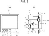
- the power device 30 is a semiconductor chip having a large area, and includes a temperature sensitive element 37 and a sense element 39 in an end of the chip as illustrated in a view (b) of FIG. 3 .
- the temperature sensitive element 37 is connected to the outside of the chip via a pad 37a and a pad 37b, and the sense element 39 has its source terminal connected to the outside via a pad 36.
- the gate is connected to the gate drive circuit 26 via a pad 35.
- the source terminal of the main element is a pad 34, and the drain terminal common to the main element and the sense element is connected via a pad 38 on the back surface of the chip.
- the inverter circuit 22 outputs a sinusoidal current as illustrated in the upper part of FIG. 4
- the power device 30 when the power device 30 is caused to perform switching and a current flows, a power loss occurs in synchronization with an output current in the power device 30.
- the power device 30 generates heat, and a main-element temperature Tm varies in synchronization with the output current as indicated by a solid line in the middle part of FIG. 4 .
- the sense element in the end of the chip has high coolability and heat in the central portion of the chip is transmitted thereto with a delay.
- a sense-element temperature Ts has an amplitude smaller than that of Tm and varies with a delay behind Tm.
- a temperature difference ⁇ T between the main element and the sense element varies with time.
- ⁇ T has different values depending on the frequency and amplitude of an output current of the inverter.
- T is an element temperature
- Rs(T) is the on-resistance of the sense element
- Rm(T) is the on-resistance of the main element.
- the on-resistance of each element typically has a characteristic of increasing with temperature rise as illustrated in FIG. 5 .
- T M T S + ⁇ T
- information about the sense ratio that is prepared in advance for estimating the main current from the sense current is a sense ratio at a certain fixed temperature difference ⁇ T0.
- ⁇ T0 a certain fixed temperature difference
- a deviation of the sense ratio caused by ⁇ T can be expressed as a coefficient K of M0 (T) as in the following Expression (5).
- K real T S K ⁇ M 0 T S
- K R M Ts + ⁇ T 0 R M Ts + ⁇ T
- K is the ratio between the on-resistance of the main element at a temperature of Ts + ⁇ T0 and the on-resistance at a temperature of Ts + ⁇ T.
- Rm (T) of the on-resistance of the main element the temperature difference ⁇ T0 between the main element and the sense element obtained in a case where the sense ratio is pre-acquired, and the temperature difference ⁇ T during the actual operation are known
- K can be obtained.
- a correct value of the sense ratio Mreal can be acquired, so that the main current can be estimated with high accuracy.
- a first embodiment is an embodiment of a power conversion apparatus that derives the above-described coefficient K and corrects an estimated current value using the coefficient K.
- the first embodiment is an embodiment of a power conversion apparatus that includes: an inverter circuit including a device having a main element and a sense element; a temporary-main-current estimator configured to estimate a current flowing through the main element, from a sense current flowing through the sense element, as a temporary main current; a temperature-difference estimator configured to estimate a temperature difference between the main element and the sense element based on a gate drive signal for the main element and the temporary main current; a main-current corrector configured to correct the temporary main current using the estimated temperature difference and a temperature characteristic of on-resistance of the main element and output the corrected temporary main current as a corrected main current; and an inverter control circuit configured to output the gate drive signal based on the corrected main current.
- a sense current of the power device 30 is detected by a sense-current detector 42 as illustrated in FIG. 6 .
- a temporary-main-current estimator 43 acquires a temporary main current value Ime' including a temperature-difference-induced error described above, from the detected sense current Is.
- a temperature-difference estimator 44 calculates an estimated value ⁇ Te of a temperature difference between the main element and the sense element by using the temporary main current and a gate drive signal.
- a main-current corrector 45 calculates a correction coefficient from the estimated temperature difference ⁇ Te and the temperature characteristic of the on-resistance, acquires the main current Ime in which the temperature-difference-induced error has been corrected by the correction coefficient, and inputs the corrected main current Ime to the inverter control circuit 24 to perform real-time control of the inverter circuit.
- the temporary-main-current estimator 43, the temperature-difference estimator 44, and the main-current corrector 45 will be sequentially described.
- the temporary-main-current estimator 43 includes a memory 432 in which the pre-acquired sense ratio M0 is stored.
- the temporary-main-current calculator 431 outputs a temporary main current Ime'.
- the temporary-main-current estimator 43 estimates the temporary main current Ime' based on the sense ratio that is the pre-acquired ratio between the main current and the sense current, and the sense current Is.
- the sense ratio has a temperature characteristic due to non-uniformity of the structure of the power device 30 in some cases.
- the sense ratio stored in the memory 432 may be in the form of a table having temperature dependence.
- the temporary-main-current estimator 43 may perform temperature correction using the sense-element temperature Ts acquired by a sense-element temperature detector 41.
- the sense ratio has current dependence in some cases.
- the sense ratio may be in the form of a table having dependence on a sense current.
- the power device 30 includes a temperature sensitive element, and the temporary-main-current estimator 43 can perform temperature correction of a temporary main current based on the sense-element temperature Ts detected by the sense-element temperature detector 41 in response to an output of the temperature sensitive element.
- the temperature-difference estimator 44 has a role of estimating the temperature difference ⁇ T between the main element and the sense element, and includes a chip-loss calculator 442 that calculates an estimated loss Ee based on the temporary main current Ime', and a temperature-difference calculator 441 that calculates an estimated temperature difference based on the estimated loss.
- the temperature difference ⁇ T is a temperature difference inside the chip, and it is not easy to acquire the temperature of the central portion of the chip as described above. Thus, the temperature difference ⁇ T is acquired by estimation based on the operation state of the power device 30. Specifically, the temperature-difference estimator 44 estimates a loss generated in the power device 30, and calculates ⁇ T in real time from a pre-acquired loss, using thermal resistance to the temperature difference.
- a loss of the power device 30 includes a conduction loss caused by flow of the main current through the main element having on-resistance and a switching loss generated at each PWM switching instant during a power conversion operation.
- a loss Eloss in one PWM cycle is expressed by the following Expression (8), where D is a duty ratio of PWM, FPWM is a PWM frequency, Eon is a turn-on loss, and Eoff is a turn-off loss. [Expression 8]
- E LOSS D F PWM I M 2 R M + E on + E off
- the first term represents a conduction loss and the second and third terms represent a switching loss.
- the chip-loss calculator 442 calculates a loss according to Expression (8) and outputs an estimated loss Ee at each PWM switching instant.
- the duty ratio and the frequency of PWM that are required for calculation of the conduction loss can be acquired by monitoring of a gate drive signal output by the inverter control circuit 24.
- the duty ratio and the frequency are not necessarily required to be acquired from the gate drive signal, and may be separately acquired in the form of data from inverter control. Further, as the main current IM, the estimated temporary main current value Ime' having already been acquired can be approximately used.
- the on-resistance Rm of the main element one having been acquired in advance is stored a memory 445 and is used for calculation of the conduction loss.
- the switching loss it is general that the switching loss is proportional to the main current value, and thus, Eon + Eoff having been acquired in advance is stored in a memory 444 in the form of a table with respect to the main current.
- the on-resistance, the turn-on loss, and the turn-off loss have temperature dependence.
- the chip-loss calculator 442 may perform temperature correction using the sense-element temperature Ts detected by the sense-element temperature detector 41. In this case, data about the temperature dependence of the on-resistance, the turn-on loss, and the turn-off loss may be stored in the memory 445 and the memory 444.
- ⁇ T is calculated and estimated using the estimated loss Ee and the pre-acquired thermal resistance.
- the power device 30 becomes a heating element due to a loss caused by current conduction during operation, and has a thermal structure that dissipates heat to the outside via a heat sink attached to the power device 30.
- FIG. 7 The above-described structure is illustrated in the form of a thermal equivalent circuit in FIG. 7 .
- a heat source caused by a loss of the power device 30.
- a heat flow from the heat source is dissipated to the periphery of the temperature T0 via thermal resistors ⁇ 0 to ⁇ N and thermal capacitors C0 to CN of the chip and the heat sink.
- the time waveform of the temperature difference ⁇ T is a result of thermal-impedance (Zm-Zs) filtering of the loss q(t).
- the temperature-difference estimator 44 passes the estimated loss Ee output at each PWM switching instant through the temperature-difference calculator 441 serving as a discrete-time filter, to acquire the estimated value ⁇ Te of the temperature difference.
- a real-time ⁇ Te is required to acquire a corrected main current Ime in real time.
- the digital filter is formed of a FIR filter, a delay of half or more of the number of taps occurs, which is not desirable.
- a configuration using an IIR filter capable of achieving a low delay as illustrated in FIG. 8 is desirable.
- the main-current corrector 45 includes a correction-coefficient calculator 451 that calculates a correction coefficient based on the estimated temperature difference, and multiplies the temporary main current by the calculated correction coefficient to obtain a corrected main current.
- the correction-coefficient calculator 451 of the main-current corrector 45 uses the estimated temperature difference ⁇ Te that is an output of the temperature-difference estimator 44, as ⁇ T.
- ⁇ Te an output of the temperature-difference estimator 44
- a pre-acquired temperature coefficient of the on-resistance of the main element is stored in a memory 453 and is multiplied by ⁇ Te in the correction-coefficient calculator 451, thereby acquiring the correction coefficient K. That is, the sense ratio is corrected using the pre-stored temperature characteristic of the on-resistance of the power device, and the main current can be accurately estimated from the sense current.
- the sense ratio is corrected using the pre-stored temperature characteristic of the on-resistance of the power device, and the main current can be accurately estimated from the sense current.
- the temporary main current is multiplied by the correction coefficient K obtained by calculation in the main-current corrector 45, so that a corrected main current is acquired, and then is output to the inverter control circuit 24.
- a main current is estimated in consideration of a temperature difference, which enables accurate current estimation of a power device using observation of a sense current.
- the correction-coefficient calculator 451 is required to include a divider.
- a second embodiment is an embodiment of a power conversion apparatus including a calculator that corrects a main current at a higher speed than that in the first embodiment.
- the second embodiment is an embodiment of a power conversion apparatus in which a temperature-difference estimator estimates a temperature difference between a main element and a sense element based on an intended driving condition for a device, such as an intended main current value in next switching and a pulse width thereof.
- a result of estimation of a main current is used for real-time control of the inverter circuit, and thus calculation of estimating the main current from a sense current needs to be performed with a low delay.
- Correction calculation is basically a sum-of-products calculation involving memory access, and one of the most time-consuming calculators is the temperature-difference calculator 441 of the temperature-difference estimator 44. This is because the temperature-difference calculator 441, like the IIR filter illustrated in FIG. 8 , is required to perform sum-of-products calculation many times.
- FIG. 9 illustrates a configuration of the power conversion apparatus of the present embodiment in which a chip loss is predicted before it occurs and a temperature difference is calculated in advance in order to reduce a delay in estimation of a temperature difference.
- the inverter control circuit 24 transmits an intended driving condition, specifically, an intended main current value in a next PWM cycle and a pulse width thereof, to the temperature-difference estimator 44.
- an intended driving condition specifically, an intended main current value in a next PWM cycle and a pulse width thereof
- a desired current value and an intended pulse width in next switching are known as an intended driving condition before the gate is driven.
- the temperature-difference estimator 44 can predict a loss value of the next switching before it occurs.
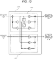
- FIG. 10 illustrates a configuration example of the temperature-difference prediction calculator 441b.
- the temperature-difference prediction calculator 441b calculates a predicted value ⁇ Tep of the estimated temperature difference ⁇ Te in the next switching by using the predicted loss Ep.
- the temperature-difference calculator 441 in FIG. 8 according to the first embodiment is provided, and further, a second temperature-difference calculator 4411 that performs calculation using an internal state signal and the predicted loss Ep extracted from the calculator 441 is provided.
- C n B n + A n B 0
- a temperature difference can be acquired as a predicted value before switching, and after detection of a sense current, the corrected main current Ime can be acquired only with a delay in the temporary-main-current estimator 43 and the main-current corrector 45.
- This enables low-delay current sensing and can provide a power conversion apparatus including a calculator that can correct a main current at a high speed.
- a third embodiment is an embodiment of a power conversion apparatus including a calculator that corrects a main current more accurately than the power conversion apparatus in the first embodiment.
- the third embodiment is an embodiment of a power conversion apparatus that includes: a second temperature-difference estimator configured to estimate a temperature difference from the corrected main current; and a second main-current corrector configured to calculate a second correction coefficient based on a second estimated temperature difference estimated by the second temperature-difference estimator and multiply the corrected main current by the second correction coefficient.
- the temporary main current Ime' including an error is used to calculate a chip loss.
- a conduction loss in a chip loss is proportional to the square of a current.
- an error in the temporary main current Ime' with respect to the actual main current Im significantly affects an error in a chip loss.
- An error in a chip loss causes an error in the estimated temperature difference ⁇ Te, and finally causes an error in the estimated main current value Ime.
- the more accurate a main current value used in the temperature-difference estimator the more accurate Ime.
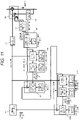
- FIG. 11 illustrates a configuration according to the present embodiment in a case where the above-described operation is repeated twice.
- a second temperature-difference estimator 44b and a second main-current corrector 45b operate upon receipt of an input of a second temporary main current Ime" corresponding to the corrected main current output by the main-current corrector 45.
- Ime is more accurate than Ime' by the amount that the influence of a temperature difference is removed.
- a second estimated temperature difference ⁇ Te' output by the second temperature-difference estimator 44b is more accurate than the former estimated temperature difference ⁇ Te
- the corrected main current Ime output by the second main-current corrector 45b is more accurate than the second temporary main current Ime".
- the temperature-difference estimator 44 and the second temperature-difference estimator 44b having the same configuration and the main-current corrector 45 and the second main-current corrector 45b having the same configuration are arranged in series in FIG. 11 , this configuration is not necessarily required.
- By additionally preparing a sequencer it is also possible to repeatedly use one same temperature-difference estimator and one same main-current corrector, thereby reducing the scales of the memory and the calculator. Further, the number of repetitions is not limited to two, and may be three or more.
- the present invention can also be applied to other power conversion apparatuses.
- a power conversion apparatus including a MOSFET that controls a current flowing through an electromagnetic coil included in an electromagnetic drive mechanism the present invention can be applied to an overcurrent detection apparatus that detects an overcurrent flowing through the MOSFET to protect the MOSFET.
- the electromagnetic drive mechanism include an electromagnetic flow-rate control valve that regulates a controlled quantity of oil in a continuously variable transmission (CVT) provided in an automobile, a direct-injection fuel injection valve that directly injects fuel into a combustion chamber of an internal combustion engine, and the like.
- CVT continuously variable transmission
Landscapes
- Engineering & Computer Science (AREA)
- Power Engineering (AREA)
- Physics & Mathematics (AREA)
- General Physics & Mathematics (AREA)
- Inverter Devices (AREA)
- Power Conversion In General (AREA)
Abstract
Description
- The present invention relates to a power conversion apparatus including a power device, and particularly relates to a power conversion apparatus that requires highly accurate current measurement.
- As next-generation automobiles, hybrid vehicles in which a combination of an internal combustion engine and an electric motor rotates driving wheels and electric vehicles in which only an electric motor rotates driving wheels have been attracting attention. As an automobile motor used in such vehicles as cited above, a compact and high-torque synchronous motor in which a permanent magnet is embedded in a rotor is adopted. Then, to produce the highest possible torque of the synchronous motor, vector control is used in general.
- In such vector control, a current command is calculated from a torque command generated by an accelerator command or a brake command, and a speed. In response to the current command, a PWM signal is generated to drive a power device of an inverter. The vector control requires a current sensor for measuring an output current of the inverter. For this reason, a sense element exclusively used for current detection is provided in addition to a main control element such as an IGBT or a MOSFET forming the power device. A current (sense current) flowing through the sense element is detected, whereby a main current flowing through the main control element is estimated. Such a power conversion circuit is disclosed in
PTL 1, for example. - Such a power device including a sense element and a main control element as described above has temperature dependence. This causes a problem of incapability of achieving accurate current measurement due to variation in a sense-current characteristic with a temperature. In view of this, according to
PTL 1, a temperature detection diode is formed in a semiconductor substrate forming a power device, and a current characteristic is corrected by the temperature detection diode. - PTL 1:
JP 2006-271098 A - Meanwhile, in a case where the temperature of a power device is measured using a temperature sensitive element such as the above-described temperature detection diode, only the temperature of a position where the temperature sensitive element is present in the power device can be measured. In some cases, a power device is formed of a semiconductor chip having a large area exceeding one mm square, and the power device itself serves as a heating element during operation. Thus, the temperature inside the chip is not uniform, and the central portion and the end in the chip have a temperature difference. In most cases, the temperature of the central portion of a chip where heat is more likely to be accumulated is higher than the temperature of the end of the chip. Of the two portions, the end of a chip is suitable as a position where a temperature sensitive element is placed. The reasons are as follows. A power device, in which both surfaces of a chip serve as drain or source terminals for the purpose of improving low on-resistance and coolability, is fitted between metals serving as both of an electrode and a heat sink. Thus, in the central portion of the chip, a pad that is used for a temperature sensitive element and can be connected to a bonding wire cannot be placed. Alternatively, in a case where a temperature sensitive element alone is placed in the central portion, away from a pad, and the temperature sensitive element and the pad placed in the end of a chip are connected by wires, the wired portion is an inactive area that does not function as a power device. This reduces the area efficiency to increase the cost. The same applies to a sense element, and it can be said that it is necessary to place the sense element, as well as a temperature sensitive element, in the end of a chip in order to achieve low on-resistance, low thermal resistance, and low cost for a power device.
- Specifically, in measurement of the temperature of a chip using a temperature sensitive element, an example of which is described in the above-cited
PTL 1, a measured temperature is the temperature of the end of the chip, in other words, the temperature of only a sense element. The temperature of a main control element (hereinafter referred to as a main element) cannot be measured, and is different from the temperature of the sense element. In the meantime, a power device such as an IGBT and a MOSFET is a semiconductor, and thus its on-resistance has temperature dependence. Because of parallel connection of the main element and the sense element, variation in temperature difference between the main element and the sense element causes variation in a ratio (sense ratio) between a main current (hereinafter referred to as a main current) and a sense current. That is, in a case where a temperature difference between a main element and a sense element is not taken into consideration as inPTL 1, an error occurs in estimation of the main current, causing a problem of reduced accuracy. - An object of the present invention is to provide a power conversion apparatus that can accurately estimate a main current using observation of a sense current by estimating the main current in consideration of a temperature difference, for a power device including a sense element.
- To attain the above-described object, the present invention provides a power conversion apparatus that includes: an inverter circuit including a device having a main element and a sense element; a temporary-main-current estimator configured to estimate a current flowing through the main element, from a sense current flowing through the sense element, as a temporary main current; a temperature-difference estimator configured to estimate a temperature difference between the main element and the sense element based on a gate drive signal for the main element and the temporary main current; a main-current corrector configured to correct the temporary main current using the estimated temperature difference and a temperature characteristic of on-resistance of the main element and output the corrected temporary main current as a corrected main current; and an inverter control circuit configured to output the gate drive signal based on the corrected main current.
- According to the present invention, in a device having a sense element mounted thereon, a main current flowing through the device can be accurately estimated using a chip temperature detected in the end of a chip, and a sense current.
-
- [
FIG. 1] FIG. 1 is a view illustrating an example of a system configuration of a hybrid vehicle. - [
FIG. 2] FIG. 2 is a view illustrating an example of a circuit configuration of a power conversion apparatus in the system ofFIG. 1 . - [
FIG. 3] FIG. 3 includes views illustrating a configuration of a power device used in the power conversion apparatus of each embodiment. - [
FIG. 4] FIG. 4 is a characteristic chart indicating an example of variation with time in a main-element temperature, a sense-element temperature, and a sense ratio. - [
FIG. 5] FIG. 5 is a characteristic chart indicating a typical temperature characteristic of on-resistance of the power device. - [
FIG. 6] FIG. 6 is a view illustrating a configuration example of a power conversion apparatus according to a first embodiment. - [
FIG. 7] FIG. 7 is a thermal equivalent circuit diagram illustrating a model example of thermal resistance of the power device. - [
FIG. 8] FIG. 8 is a view illustrating a configuration example of a temperature-difference calculator of the power conversion apparatus according to the first embodiment. - [
FIG. 9] FIG. 9 is a view illustrating a configuration example of a power conversion apparatus according to a second embodiment. - [
FIG. 10] FIG. 10 is a view illustrating a configuration example of a temperature-difference calculator of the power conversion apparatus according to the second embodiment. - [
FIG. 11] FIG. 11 is a view illustrating a configuration example of a power conversion apparatus according to a third embodiment. - Hereinafter, embodiments of the present invention will be described in detail with reference to the drawings. However, the present invention is not limited to the following embodiments, and examples of various modifications and applications are also included in the technical concept of the present invention.
- First, a power conversion apparatus to which various embodiments of the present invention are applied will be described with reference to the drawings. While a power conversion apparatus according to each embodiment can be typically applied to a hybrid vehicle or an electric vehicle, the following description will be made about a case where the power conversion apparatus is applied to a hybrid vehicle as one example. However, it is a matter of course that the power conversion apparatus of each embodiment can be used not only for a hybrid vehicle and an electric vehicle, but also as a power conversion apparatus of an electric motor used for other industrial equipment.
-
FIG. 1 illustrates an example of a system configuration of a hybrid vehicle. Aninternal combustion engine 10 and amotor generator 11 are power sources that generate traveling torque of the vehicle. Further, themotor generator 11 not only generates rotary torque as an electric motor, but also has a power generating function of converting rotary force that is mechanical energy applied to themotor generator 11, into electric power. - As described above, the
motor generator 11 operates as not only an electric motor but also a power generator depending on a method of driving the vehicle. - An output of the
internal combustion engine 10 is transmitted to themotor generator 11 via apower distribution mechanism 12, and rotary torque from thepower distribution mechanism 12 or rotary torque generated by themotor generator 11 is transmitted towheels 15 via atransmission 13 and adifferential gear 14. - On the other hand, during a regenerative braking operation, rotary torque is transmitted from the
wheels 15 to themotor generator 11, and themotor generator 11 generates AC power based on the transmitted rotary torque. The generated AC power is converted into DC power by apower conversion apparatus 20. The DC power is charged into a high-voltage battery 21, and the charged power is used again as travelling energy. - The
power conversion apparatus 20 includes aninverter circuit 22 and a smoothingcapacitor 23. Theinverter circuit 22 is electrically connected to thebattery 21 via the smoothingcapacitor 23, and power is transmitted between thebattery 21 and theinverter circuit 22. The smoothingcapacitor 23 smooths DC power supplied to theinverter circuit 22. - A
control circuit 24 for theinverter circuit 22 of thepower conversion apparatus 20 receives a command from a host control device via aconnector 25 for communication or transmits data indicating an operating state to the host control device. Thecontrol circuit 24 calculates a controlled quantity of themotor generator 11 in response to a command as input, generates a control signal based on a result of the calculation, and supplies the control signal to agate drive circuit 26. In response to the control signal, thegate drive circuit 26 generates a drive signal for controlling theinverter circuit 22. - In a case where the
motor generator 11 is caused to operate as an electric motor, theinverter circuit 22 generates AC power based on DC power supplied from thebattery 21 and supplies the AC power to themotor generator 11. Themotor generator 11 and theinverter circuit 22 form a drive mechanism that operates as a motor-generator unit. -
FIG. 2 is a view illustrating a circuit configuration of thepower conversion apparatus 20 in the system. The following description will be made about an example of a power device using a MOSFET. Thepower conversion apparatus 20 includes upper arms and lower arms each including acontrol MOSFET 31 forming apower device 30 and adiode 32, for three phases of U phase, V phase, and W phase of AC power. - These three-phase upper and lower arms form the
inverter circuit 22. Meanwhile, thecontrol MOSFET 31 will be referred to as a "main control element" in relation to a sense element, where appropriate. - A drain terminal of the upper-
arm control MOSFET 31 is electrically connected to a positive-electrode-side capacitor terminal of the smoothingcapacitor 23, and a source terminal of the lower-arm MOSFET 31 is electrically connected to a negative-electrode-side capacitor terminal of the smoothingcapacitor 23. Thus, thecontrol MOSFET 31 includes a drain terminal, a source terminal, and a gate terminal. Further, thediode 32 is electrically connected in parallel between the drain terminal and the source terminal. - The
gate drive circuit 26 is provided between the source terminal and the gate terminal of thecontrol MOSFET 31, and controls turn-on and turn-off of thecontrol MOSFET 31. Thecontrol circuit 24 for the inverter circuit supplies a control signal to the plurality ofgate drive circuits 26. - The lower-
arm power device 30 is provided with a sense element for current detection arranged in parallel with thecontrol MOSFET 31. Also the sense element is formed of a MOSFET, and a sense current flowing through its source terminal is input to acurrent detection circuit 33. Then, the speed of a rotor and the position of a magnetic pole are calculated based on a current detected by thecurrent detection circuit 33 and a voltage measured separately from the current. By using the calculated values, the rotary torque and the rotational speed are controlled. - As described above, the
control circuit 24 for theinverter circuit 22 receives a control command from the host control device, generates a control signal for controlling thepower devices 30 forming the upper arms and the lower arms of theinverter circuit 22 in response to the control command, and supplies the control signal to thegate drive circuits 26. In response to the control signal, thegate drive circuits 26 supply drive signals for driving thepower devices 30 forming the upper and lower arms of each phase, to thepower devices 30 of each phase. - The
control MOSFET 31 of thepower device 30 is turned on or off in response to the drive signal from thegate drive circuit 26, to convert DC power supplied from thebattery 21 into three-phase AC power. The AC power is supplied to themotor generator 11. Such a power conversion apparatus as having the above-described configuration is already well known. - Meanwhile, as illustrated in a view (a) of
FIG. 3 , thepower device 30 is a semiconductor chip having a large area, and includes a temperaturesensitive element 37 and asense element 39 in an end of the chip as illustrated in a view (b) ofFIG. 3 . The temperaturesensitive element 37 is connected to the outside of the chip via apad 37a and apad 37b, and thesense element 39 has its source terminal connected to the outside via apad 36. Further, the gate is connected to thegate drive circuit 26 via apad 35. The source terminal of the main element is apad 34, and the drain terminal common to the main element and the sense element is connected via apad 38 on the back surface of the chip. - In this regard, in a case where the
inverter circuit 22 outputs a sinusoidal current as illustrated in the upper part ofFIG. 4 , when thepower device 30 is caused to perform switching and a current flows, a power loss occurs in synchronization with an output current in thepower device 30. Then, thepower device 30 generates heat, and a main-element temperature Tm varies in synchronization with the output current as indicated by a solid line in the middle part ofFIG. 4 . On the other hand, the sense element in the end of the chip has high coolability and heat in the central portion of the chip is transmitted thereto with a delay. Thus, as illustrated by a broken line in the middle part ofFIG. 4 , a sense-element temperature Ts has an amplitude smaller than that of Tm and varies with a delay behind Tm. In other words, a temperature difference ΔT between the main element and the sense element varies with time. Further, ΔT has different values depending on the frequency and amplitude of an output current of the inverter. - The influence of the temperature difference ΔT on the accuracy of current estimation will be described. First, suppose that T is an element temperature, Rs(T) is the on-resistance of the sense element, and Rm(T) is the on-resistance of the main element. In a case where the power device is a SiC-MOSFETd, the on-resistance of each element typically has a characteristic of increasing with temperature rise as illustrated in
FIG. 5 . - A sense ratio M can be described as the following Expression (1).
[Expression 1]
- The relationship between Ts and Tm is as expressed by the following Expression (2) using ΔT.
[Expression 2]
- In this regard, information about the sense ratio that is prepared in advance for estimating the main current from the sense current is a sense ratio at a certain fixed temperature difference ΔT0. For example, in a case where the temperature characteristic of the sense ratio is pre-acquired using a thermostatic tank, the sense element and the main element are externally heated to a uniform temperature, so that ΔT0 is equal to zero. Then, with the sense ratio at that time being represented as M0(T), the following Expression (3) is given.
[Expression 3]
- On the other hand, while the device is operating and generating heat, a sense ratio Mreal is as expressed by the following Expression (4).
[Expression 4]
- As long as the actual temperature difference ΔT is different from the temperature difference ΔT0 obtained in a case where the sense ratio is pre-acquired, M0(T) ≠ Mreal(T). Thus, the sense ratio varies more than expected depending on the difference between ΔT and ΔT0, which causes a temperature-difference-induced error in current estimation.
- A deviation of the sense ratio caused by ΔT can be expressed as a coefficient K of M0 (T) as in the following Expression (5).
[Expression 5]
- In Expression (5), K is a coefficient defined by the following Expression (6).
[Expression 6]
- As indicated by Expression (6), K is the ratio between the on-resistance of the main element at a temperature of Ts + ΔT0 and the on-resistance at a temperature of Ts + ΔT. Specifically, when the temperature characteristic Rm (T) of the on-resistance of the main element, the temperature difference ΔT0 between the main element and the sense element obtained in a case where the sense ratio is pre-acquired, and the temperature difference ΔT during the actual operation are known, K can be obtained. As a result, a correct value of the sense ratio Mreal can be acquired, so that the main current can be estimated with high accuracy.
- In this regard, it is possible to make Rm(T) known by pre-acquiring the characteristic, and it is also possible to make ΔT0 equal to zero by placing the device in a constant-temperature state at the time of pre-acquiring the sense ratio. As can be seen therefrom, only by knowing ΔT that varies with time depending on the operating state of the power device in real time, it is possible to derive the coefficient K, thereby acquiring the correct sense ratio Mreal in real time. That is, the sense ratio is corrected using the pre-stored temperature characteristic of the on-resistance of the power device, and the main current can be accurately estimated from the sense current.
- A first embodiment is an embodiment of a power conversion apparatus that derives the above-described coefficient K and corrects an estimated current value using the coefficient K. Specifically, the first embodiment is an embodiment of a power conversion apparatus that includes: an inverter circuit including a device having a main element and a sense element; a temporary-main-current estimator configured to estimate a current flowing through the main element, from a sense current flowing through the sense element, as a temporary main current; a temperature-difference estimator configured to estimate a temperature difference between the main element and the sense element based on a gate drive signal for the main element and the temporary main current; a main-current corrector configured to correct the temporary main current using the estimated temperature difference and a temperature characteristic of on-resistance of the main element and output the corrected temporary main current as a corrected main current; and an inverter control circuit configured to output the gate drive signal based on the corrected main current.
- In the power conversion apparatus according to the present embodiment, a sense current of the
power device 30 is detected by a sense-current detector 42 as illustrated inFIG. 6 . A temporary-main-current estimator 43 acquires a temporary main current value Ime' including a temperature-difference-induced error described above, from the detected sense current Is. Then, a temperature-difference estimator 44 calculates an estimated value ΔTe of a temperature difference between the main element and the sense element by using the temporary main current and a gate drive signal. Finally, a main-current corrector 45 calculates a correction coefficient from the estimated temperature difference ΔTe and the temperature characteristic of the on-resistance, acquires the main current Ime in which the temperature-difference-induced error has been corrected by the correction coefficient, and inputs the corrected main current Ime to theinverter control circuit 24 to perform real-time control of the inverter circuit. Hereinafter, the temporary-main-current estimator 43, the temperature-difference estimator 44, and the main-current corrector 45 will be sequentially described. - The temporary-main-
current estimator 43 includes amemory 432 in which the pre-acquired sense ratio M0 is stored. A temporary-main-current calculator 431 performs multiplication of the following Expression (7) for the sense current Is acquired by the sense-current detector 42.
[Expression 7]
- Then, the temporary-main-
current calculator 431 outputs a temporary main current Ime'. In other words, the temporary-main-current estimator 43 estimates the temporary main current Ime' based on the sense ratio that is the pre-acquired ratio between the main current and the sense current, and the sense current Is. - In this regard, the sense ratio has a temperature characteristic due to non-uniformity of the structure of the
power device 30 in some cases. For this reason, the sense ratio stored in thememory 432 may be in the form of a table having temperature dependence. In this case, the temporary-main-current estimator 43 may perform temperature correction using the sense-element temperature Ts acquired by a sense-element temperature detector 41. Alternatively, in the same manner as in the above-described case, the sense ratio has current dependence in some cases. In this case, the sense ratio may be in the form of a table having dependence on a sense current. In either case, thepower device 30 includes a temperature sensitive element, and the temporary-main-current estimator 43 can perform temperature correction of a temporary main current based on the sense-element temperature Ts detected by the sense-element temperature detector 41 in response to an output of the temperature sensitive element. - The temperature-
difference estimator 44 has a role of estimating the temperature difference ΔT between the main element and the sense element, and includes a chip-loss calculator 442 that calculates an estimated loss Ee based on the temporary main current Ime', and a temperature-difference calculator 441 that calculates an estimated temperature difference based on the estimated loss. The temperature difference ΔT is a temperature difference inside the chip, and it is not easy to acquire the temperature of the central portion of the chip as described above. Thus, the temperature difference ΔT is acquired by estimation based on the operation state of thepower device 30. Specifically, the temperature-difference estimator 44 estimates a loss generated in thepower device 30, and calculates ΔT in real time from a pre-acquired loss, using thermal resistance to the temperature difference. - First, an example of a configuration for loss estimation of the
power device 30 will be described. A loss of thepower device 30 includes a conduction loss caused by flow of the main current through the main element having on-resistance and a switching loss generated at each PWM switching instant during a power conversion operation. A loss Eloss in one PWM cycle is expressed by the following Expression (8), where D is a duty ratio of PWM, FPWM is a PWM frequency, Eon is a turn-on loss, and Eoff is a turn-off loss.
[Expression 8]
- The first term represents a conduction loss and the second and third terms represent a switching loss. The chip-
loss calculator 442 calculates a loss according to Expression (8) and outputs an estimated loss Ee at each PWM switching instant. The duty ratio and the frequency of PWM that are required for calculation of the conduction loss can be acquired by monitoring of a gate drive signal output by theinverter control circuit 24. The duty ratio and the frequency are not necessarily required to be acquired from the gate drive signal, and may be separately acquired in the form of data from inverter control. Further, as the main current IM, the estimated temporary main current value Ime' having already been acquired can be approximately used. With regard to the on-resistance Rm of the main element, one having been acquired in advance is stored amemory 445 and is used for calculation of the conduction loss. With regard to the switching loss, it is general that the switching loss is proportional to the main current value, and thus, Eon + Eoff having been acquired in advance is stored in amemory 444 in the form of a table with respect to the main current. In some cases, the on-resistance, the turn-on loss, and the turn-off loss have temperature dependence. In such a case, the chip-loss calculator 442 may perform temperature correction using the sense-element temperature Ts detected by the sense-element temperature detector 41. In this case, data about the temperature dependence of the on-resistance, the turn-on loss, and the turn-off loss may be stored in thememory 445 and thememory 444. - Secondly, an example of a configuration for estimation of the temperature difference ΔT using the estimated loss Ee will be described. ΔT is calculated and estimated using the estimated loss Ee and the pre-acquired thermal resistance. The
power device 30 becomes a heating element due to a loss caused by current conduction during operation, and has a thermal structure that dissipates heat to the outside via a heat sink attached to thepower device 30. - The above-described structure is illustrated in the form of a thermal equivalent circuit in
FIG. 7 . At the left end ofFIG. 7 , there is a heat source caused by a loss of thepower device 30. A heat flow from the heat source is dissipated to the periphery of the temperature T0 via thermal resistors θ0 to θN and thermal capacitors C0 to CN of the chip and the heat sink. In this thermal equivalent circuit, the time waveform q(t) of the heat flow of the heat source is expressed by the following Expression (9).
[Expression 9]
- Suppose that Zm is impedance of heat transfer from the heat source to the main element and Zs is impedance of heat transfer from the heat source to the sense element. Then, the temperature Tm(s) of the main element and the temperature Ts(s) of the sense element in a frequency domain s are expressed by the following Expressions (10) and (11).
[Expression 10]
[Expression 11]
- In the expressions, Q(s) is q(t) in the frequency domain. The temperature difference ΔT is as expressed by the following Expression (12).
[Expression 12]
- As can be seen therefrom, the time waveform of the temperature difference ΔT is a result of thermal-impedance (Zm-Zs) filtering of the loss q(t). The temperature-
difference estimator 44 passes the estimated loss Ee output at each PWM switching instant through the temperature-difference calculator 441 serving as a discrete-time filter, to acquire the estimated value ΔTe of the temperature difference. - In this regard, a real-time ΔTe is required to acquire a corrected main current Ime in real time. This requires a low-delay digital filter as a digital filter forming the temperature-difference calculator. In a case where the digital filter is formed of a FIR filter, a delay of half or more of the number of taps occurs, which is not desirable. A configuration using an IIR filter capable of achieving a low delay as illustrated in
FIG. 8 is desirable. Tap coefficients An and Bn (n = 1, 2, 3,...) of an IIR filter that achieves the thermal impedance (Zm-Zs) are stored in thememory 443 and used by the temperature-difference estimator 441. - Lastly, a configuration example of the main-
current corrector 45 will be described. The main-current corrector 45 includes a correction-coefficient calculator 451 that calculates a correction coefficient based on the estimated temperature difference, and multiplies the temporary main current by the calculated correction coefficient to obtain a corrected main current. The temporary main current Ime' output by the temporary-main-current estimator 43 is already a value corresponding to a result of multiplication of the sense current Is by the sense ratio M0 at the temperature difference ΔT = 0. Thus, when Ime' is multiplied by the correction coefficient K, the estimated main current value Ime that should be acquired by multiplication of Is by the sense ratio Mreal that takes into account the temperature difference, is acquired. The correction coefficient K may be calculated according to Expression (6) or may be calculated according to the following Expression (13) that is a first-order approximation thereof.
[Expression 13]
- The correction-
coefficient calculator 451 of the main-current corrector 45 uses the estimated temperature difference ΔTe that is an output of the temperature-difference estimator 44, as ΔT. In a case where the configuration of calculating the correction coefficient K according to Expression (13) is employed, a pre-acquired temperature coefficient of the on-resistance of the main element is stored in amemory 453 and is multiplied by ΔTe in the correction-coefficient calculator 451, thereby acquiring the correction coefficient K. That is, the sense ratio is corrected using the pre-stored temperature characteristic of the on-resistance of the power device, and the main current can be accurately estimated from the sense current. That is, the sense ratio is corrected using the pre-stored temperature characteristic of the on-resistance of the power device, and the main current can be accurately estimated from the sense current. The temporary main current is multiplied by the correction coefficient K obtained by calculation in the main-current corrector 45, so that a corrected main current is acquired, and then is output to theinverter control circuit 24. - As described above, with the power conversion apparatus according to the present embodiment, a main current is estimated in consideration of a temperature difference, which enables accurate current estimation of a power device using observation of a sense current.
- Additionally, in a case where the configuration of performing the calculation according to Expression (6) is employed to obtain a more accurate result, it is only required to store the on-resistance of the main element at each of pre-acquired temperatures in the
memory 453. However, in this case, the correction-coefficient calculator 451 is required to include a divider. Thus, under a condition where a sufficient hardware scale and a sufficient calculation speed are unavailable, it is desirable to employ the configuration using Expression (13). - A second embodiment is an embodiment of a power conversion apparatus including a calculator that corrects a main current at a higher speed than that in the first embodiment. Specifically, the second embodiment is an embodiment of a power conversion apparatus in which a temperature-difference estimator estimates a temperature difference between a main element and a sense element based on an intended driving condition for a device, such as an intended main current value in next switching and a pulse width thereof.
- A result of estimation of a main current is used for real-time control of the inverter circuit, and thus calculation of estimating the main current from a sense current needs to be performed with a low delay. In a case where correction calculation is performed many times in order to increase the accuracy as in the present invention, the calculation is very likely to be not in time depending on the operation speed of a calculator. Correction calculation is basically a sum-of-products calculation involving memory access, and one of the most time-consuming calculators is the temperature-
difference calculator 441 of the temperature-difference estimator 44. This is because the temperature-difference calculator 441, like the IIR filter illustrated inFIG. 8 , is required to perform sum-of-products calculation many times. -
FIG. 9 illustrates a configuration of the power conversion apparatus of the present embodiment in which a chip loss is predicted before it occurs and a temperature difference is calculated in advance in order to reduce a delay in estimation of a temperature difference. In the present embodiment, theinverter control circuit 24 transmits an intended driving condition, specifically, an intended main current value in a next PWM cycle and a pulse width thereof, to the temperature-difference estimator 44. In theinverter control circuit 24, a desired current value and an intended pulse width in next switching are known as an intended driving condition before the gate is driven. Thus, by using these pieces of information, the temperature-difference estimator 44 can predict a loss value of the next switching before it occurs. The temperature-difference estimator 44 illustrated inFIG. 9 includes a chip-loss prediction calculator 446 for this prediction, and has a configuration similar to that of the chip-loss calculator 442 except that it receives an intended main current value in next switching and a pulse width thereof, that is, an intended driving condition. A loss value Ep in the next switching predicted by the chip-loss predictor 446, together with the estimated loss value Ee in the switching having been already performed, is output to a temperature-difference prediction calculator 441b. -
FIG. 10 illustrates a configuration example of the temperature-difference prediction calculator 441b. The temperature-difference prediction calculator 441b calculates a predicted value ΔTep of the estimated temperature difference ΔTe in the next switching by using the predicted loss Ep. In the configuration thereof, the temperature-difference calculator 441 inFIG. 8 according to the first embodiment is provided, and further, a second temperature-difference calculator 4411 that performs calculation using an internal state signal and the predicted loss Ep extracted from thecalculator 441 is provided. A tap coefficient Cn (n = 1, 2, 3,...) conforms to the definition of the following Expression (14).
[Expression 14]
- With the configuration of the power conversion circuit according to the present embodiment, a temperature difference can be acquired as a predicted value before switching, and after detection of a sense current, the corrected main current Ime can be acquired only with a delay in the temporary-main-
current estimator 43 and the main-current corrector 45. This enables low-delay current sensing and can provide a power conversion apparatus including a calculator that can correct a main current at a high speed. - A third embodiment is an embodiment of a power conversion apparatus including a calculator that corrects a main current more accurately than the power conversion apparatus in the first embodiment. Specifically, the third embodiment is an embodiment of a power conversion apparatus that includes: a second temperature-difference estimator configured to estimate a temperature difference from the corrected main current; and a second main-current corrector configured to calculate a second correction coefficient based on a second estimated temperature difference estimated by the second temperature-difference estimator and multiply the corrected main current by the second correction coefficient.
- In the first embodiment, in the temperature-
difference estimator 44, the temporary main current Ime' including an error is used to calculate a chip loss. A conduction loss in a chip loss is proportional to the square of a current. Thus, an error in the temporary main current Ime' with respect to the actual main current Im significantly affects an error in a chip loss. An error in a chip loss causes an error in the estimated temperature difference ΔTe, and finally causes an error in the estimated main current value Ime. Conversely, the more accurate a main current value used in the temperature-difference estimator, the more accurate Ime. Thus, by repeating estimation of a temperature difference and correction of a main current, it is possible to acquire a highly accurate main current. -
FIG. 11 illustrates a configuration according to the present embodiment in a case where the above-described operation is repeated twice. In the drawing, a second temperature-difference estimator 44b and a second main-current corrector 45b operate upon receipt of an input of a second temporary main current Ime" corresponding to the corrected main current output by the main-current corrector 45. Ime" is more accurate than Ime' by the amount that the influence of a temperature difference is removed. Thus, a second estimated temperature difference ΔTe' output by the second temperature-difference estimator 44b is more accurate than the former estimated temperature difference ΔTe, and the corrected main current Ime output by the second main-current corrector 45b is more accurate than the second temporary main current Ime". - Additionally, though the temperature-
difference estimator 44 and the second temperature-difference estimator 44b having the same configuration and the main-current corrector 45 and the second main-current corrector 45b having the same configuration are arranged in series inFIG. 11 , this configuration is not necessarily required. By additionally preparing a sequencer, it is also possible to repeatedly use one same temperature-difference estimator and one same main-current corrector, thereby reducing the scales of the memory and the calculator. Further, the number of repetitions is not limited to two, and may be three or more. - In each of the above-described embodiments, the power conversion apparatus that controls the electric motor has been described. However, the present invention can also be applied to other power conversion apparatuses. For example, in a power conversion apparatus including a MOSFET that controls a current flowing through an electromagnetic coil included in an electromagnetic drive mechanism, the present invention can be applied to an overcurrent detection apparatus that detects an overcurrent flowing through the MOSFET to protect the MOSFET. In this regard, examples of the electromagnetic drive mechanism include an electromagnetic flow-rate control valve that regulates a controlled quantity of oil in a continuously variable transmission (CVT) provided in an automobile, a direct-injection fuel injection valve that directly injects fuel into a combustion chamber of an internal combustion engine, and the like.
- The present invention is not limited to the above-described embodiments, and includes various modifications.
- For example, the above-described embodiments have been described in detail for easy understanding of the present invention, and are not necessarily limited to those having all the described components. Further, a part of the components of one embodiment can be replaced with the components of another embodiment, and the components of a certain embodiment can be added to the components of another embodiment. Moreover, a part of the components of each embodiment can be subjected to addition of another component, removal, and replacement with another component.
-
- 10
- internal combustion engine (EGN)
- 11
- motor generator (MG)
- 12
- power distribution mechanism (TSM)
- 13
- transmission (TM)
- 14
- differential gear (DEF)
- 15
- wheels (WH)
- 20
- power conversion apparatus
- 21
- battery (BAT)
- 22
- inverter circuit
- 23
- smoothing capacitor
- 24
- (inverter) control circuit
- 25
- connector
- 26
- gate drive circuit
- 30
- power device
- 31
- control MOSFET
- 32
- diode
- 33
- current detection circuit
- 34, 35, 36, 38
- pad
- 37
- temperature sensitive element
- 39
- sense element
- 41
- sense-element temperature detector
- 42
- sense-current detector
- 43
- temporary-main-current estimator
- 431
- temporary-main-current calculator
- 44
- temperature-difference estimator
- 441
- temperature-difference calculator
- 442
- chip-loss calculator
- 446
- chip-loss prediction calculator
- 45
- main-current corrector
- 451
- correction-coefficient calculator
Claims (10)
- A power conversion apparatus comprising:an inverter circuit including a device having a main element and a sense element;a temporary-main-current estimator configured to estimate a main current flowing through the main element, from a sense current flowing through the sense element, as a temporary main current;a temperature-difference estimator configured to output an estimated temperature difference between the main element and the sense element based on a gate drive signal for the main element and the temporary main current;a main-current corrector configured to correct the temporary main current using the estimated temperature difference and a temperature characteristic of on-resistance of the main element and output the corrected temporary main current as a corrected main current; andan inverter control circuit configured to output the gate drive signal based on the corrected main current.
- The power conversion apparatus according to claim 1, wherein
the temporary-main-current estimator estimates the temporary main current based on a sense ratio that is a pre-acquired ratio between the main current and the sense current, and the sense current. - The power conversion apparatus according to claim 2, whereinthe device includes a temperature sensitive element, andthe temporary-main-current estimator corrects a temperature of the temporary main current based on a sense-element temperature detected from an output of the temperature sensitive element.
- The power conversion apparatus according to claim 2, wherein
the temperature-difference estimator includes a chip-loss calculator that calculates an estimated loss based on the temporary main current, and a temperature-difference calculator that calculates the estimated temperature difference based on the estimated loss. - The power conversion apparatus according to claim 4, wherein
the main-current corrector includes a correction-coefficient calculator that calculates a correction coefficient based on the estimated temperature difference. - The power conversion apparatus according to claim 5, wherein
the main-current corrector multiplies the temporary main current by the correction coefficient to obtain the corrected main current. - The power conversion apparatus according to claim 6, wherein
the main-current corrector multiplies a temperature coefficient of the on-resistance of the main element and the estimated temperature difference at a temperature of the sense element, to obtain the correction coefficient. - The power conversion apparatus according to claim 1, wherein
the temperature-difference estimator estimates a temperature difference between the main element and the sense element based on an intended driving condition for the device. - The power conversion apparatus according to claim 8, wherein
the intended driving condition includes an intended main current value in next switching and a pulse width of the intended main current value. - The power conversion apparatus according to claim 1, further comprising:a second temperature-difference estimator configured to estimate a temperature difference from the corrected main current; anda second main-current corrector configured to calculate a second correction coefficient based on a second estimated temperature difference estimated by the second temperature-difference estimator and multiply the corrected main current by the second correction coefficient.
Applications Claiming Priority (2)
| Application Number | Priority Date | Filing Date | Title |
|---|---|---|---|
| JP2019225284A JP7181851B2 (en) | 2019-12-13 | 2019-12-13 | power converter |
| PCT/JP2020/044300 WO2021117512A1 (en) | 2019-12-13 | 2020-11-27 | Power conversion device |
Publications (2)
| Publication Number | Publication Date |
|---|---|
| EP4075648A1 true EP4075648A1 (en) | 2022-10-19 |
| EP4075648A4 EP4075648A4 (en) | 2023-12-20 |
Family
ID=76330192
Family Applications (1)
| Application Number | Title | Priority Date | Filing Date |
|---|---|---|---|
| EP20898135.7A Pending EP4075648A4 (en) | 2019-12-13 | 2020-11-27 | POWER CONVERSION DEVICE |
Country Status (5)
| Country | Link |
|---|---|
| US (1) | US11984822B2 (en) |
| EP (1) | EP4075648A4 (en) |
| JP (1) | JP7181851B2 (en) |
| CN (1) | CN114788156B (en) |
| WO (1) | WO2021117512A1 (en) |
Families Citing this family (5)
| Publication number | Priority date | Publication date | Assignee | Title |
|---|---|---|---|---|
| EP4002664A1 (en) * | 2020-11-11 | 2022-05-25 | Valeo Siemens eAutomotive Germany GmbH | Inverter, method for configuring an inverter, method for controlling an inverter and corresponding computer program |
| JP7818979B2 (en) * | 2022-02-15 | 2026-02-24 | 三菱重工業株式会社 | Control device, control system, and control method |
| JP7741755B2 (en) * | 2022-03-11 | 2025-09-18 | Astemo株式会社 | Current detection device for power devices and power conversion device |
| CN116865731A (en) * | 2023-01-06 | 2023-10-10 | 苏州洪芯集成电路有限公司 | Self-compensating high-precision digital PWM signal generation circuit |
| EP4417982A1 (en) * | 2023-02-17 | 2024-08-21 | Infineon Technologies Austria AG | Current sensing integrated circuit and corresponding method |
Family Cites Families (38)
| Publication number | Priority date | Publication date | Assignee | Title |
|---|---|---|---|---|
| JP3462007B2 (en) * | 1996-06-10 | 2003-11-05 | 三菱電機株式会社 | Method for detecting rotation angle and load torque of DC motor, DC motor control device, and electric power steering device |
| JP4391719B2 (en) * | 2002-03-20 | 2009-12-24 | トヨタ自動車株式会社 | Motor temperature estimation device and motor control device |
| JP2004117111A (en) * | 2002-09-25 | 2004-04-15 | Toshiba Corp | Semiconductor device |
| DE102004039392B3 (en) * | 2004-08-13 | 2005-09-15 | Cornelius Peter | Detecting current in electrical device driven by field effect transistor using pulse width modulation involves deriving current from pulse width modulation, source-daring voltage, ambient temperature and supply voltage |
| JP2006271098A (en) * | 2005-03-24 | 2006-10-05 | Hitachi Ltd | Power converter |
| JP5233198B2 (en) * | 2007-08-06 | 2013-07-10 | 富士電機株式会社 | Semiconductor device |
| JP4807443B2 (en) * | 2009-07-08 | 2011-11-02 | トヨタ自動車株式会社 | Secondary battery temperature estimation device |
| JP5317881B2 (en) * | 2009-08-05 | 2013-10-16 | 三菱電機株式会社 | Power converter and protection method for power converter |
| JP5443946B2 (en) * | 2009-11-02 | 2014-03-19 | 株式会社東芝 | Inverter device |
| JP5294335B2 (en) * | 2010-06-18 | 2013-09-18 | 三菱電機株式会社 | Semiconductor device |
| JP5372257B2 (en) * | 2010-09-03 | 2013-12-18 | 三菱電機株式会社 | Semiconductor device |
| JP5590240B2 (en) * | 2011-07-06 | 2014-09-17 | 富士電機株式会社 | Current correction circuit and current correction method for power semiconductor device |
| JP2013134927A (en) * | 2011-12-27 | 2013-07-08 | Fujitsu Component Ltd | Distribution gear |
| WO2014049808A1 (en) * | 2012-09-28 | 2014-04-03 | 株式会社日立製作所 | Power conversion device |
| JP6107936B2 (en) * | 2013-04-01 | 2017-04-05 | 富士電機株式会社 | Power converter |
| CN107888056B (en) * | 2013-07-10 | 2020-04-17 | 株式会社电装 | Drive control device |
| JP6295062B2 (en) * | 2013-11-07 | 2018-03-14 | 三菱日立パワーシステムズ株式会社 | Steam turbine plant start-up control device |
| JP6219154B2 (en) * | 2013-12-11 | 2017-10-25 | 新電元工業株式会社 | Temperature detection device |
| DE102014218708A1 (en) * | 2014-09-17 | 2016-03-17 | Continental Teves Ag & Co. Ohg | Shunt current measurement with temperature compensation |
| JP6265099B2 (en) * | 2014-10-08 | 2018-01-24 | 三菱電機株式会社 | Semiconductor device |
| JP6623556B2 (en) * | 2015-05-27 | 2019-12-25 | 株式会社デンソー | Semiconductor device |
| JP6443245B2 (en) * | 2015-07-02 | 2018-12-26 | 株式会社デンソー | Rotating electrical machine control device |
| JP6500694B2 (en) * | 2015-08-19 | 2019-04-17 | 富士電機株式会社 | Control device for power conversion device and power conversion device |
| JP6341222B2 (en) * | 2016-03-31 | 2018-06-13 | トヨタ自動車株式会社 | Power system |
| JP6673118B2 (en) * | 2016-09-23 | 2020-03-25 | 株式会社デンソー | Semiconductor device |
| CN110337784B (en) * | 2017-02-28 | 2023-06-09 | 三菱电机株式会社 | Semiconductor device and power conversion system |
| JP6776951B2 (en) * | 2017-03-06 | 2020-10-28 | 株式会社デンソー | Rotating electric machine control device and electric power steering device using this |
| WO2019202675A1 (en) * | 2018-04-18 | 2019-10-24 | 三菱電機株式会社 | Power conversion device |
| JP6908010B2 (en) * | 2018-08-28 | 2021-07-21 | 株式会社デンソー | Switch drive |
| JP7004869B2 (en) * | 2019-03-28 | 2022-01-21 | 三菱電機株式会社 | Drive and air conditioner |
| JP7343333B2 (en) * | 2019-08-27 | 2023-09-12 | 日立Astemo株式会社 | power converter |
| US11418104B2 (en) * | 2019-11-27 | 2022-08-16 | Kookmin University Industry Academy Cooperation Foundation | Current measurement method for three-phase pulse width modulation inverter using real-time switch junction temperature estimation technique and three-phase pulse width modulation inverter system |
| JP6786012B1 (en) * | 2019-11-29 | 2020-11-18 | 三菱電機株式会社 | Power converter |
| JP7219731B2 (en) * | 2020-02-03 | 2023-02-08 | 日立Astemo株式会社 | Semiconductor device driving device and power conversion device |
| JP7462474B2 (en) * | 2020-05-25 | 2024-04-05 | 日立Astemo株式会社 | Power Conversion Equipment |
| JP7385538B2 (en) * | 2020-07-31 | 2023-11-22 | 株式会社安川電機 | Power converter, temperature estimation method and program |
| WO2022045098A1 (en) * | 2020-08-25 | 2022-03-03 | サンデン・オートモーティブコンポーネント株式会社 | Inverter device, and vehicular electric compressor provided with same |
| JP7796593B2 (en) * | 2022-06-01 | 2026-01-09 | 三菱電機株式会社 | Power Conversion Device |
-
2019
- 2019-12-13 JP JP2019225284A patent/JP7181851B2/en active Active
-
2020
- 2020-11-27 WO PCT/JP2020/044300 patent/WO2021117512A1/en not_active Ceased
- 2020-11-27 CN CN202080085108.9A patent/CN114788156B/en active Active
- 2020-11-27 EP EP20898135.7A patent/EP4075648A4/en active Pending
- 2020-11-27 US US17/784,334 patent/US11984822B2/en active Active
Also Published As
| Publication number | Publication date |
|---|---|
| US11984822B2 (en) | 2024-05-14 |
| CN114788156A (en) | 2022-07-22 |
| JP2021097435A (en) | 2021-06-24 |
| EP4075648A4 (en) | 2023-12-20 |
| CN114788156B (en) | 2026-04-07 |
| US20230060086A1 (en) | 2023-02-23 |
| JP7181851B2 (en) | 2022-12-01 |
| WO2021117512A1 (en) | 2021-06-17 |
Similar Documents
| Publication | Publication Date | Title |
|---|---|---|
| US11984822B2 (en) | Power conversion apparatus | |
| CN102472796B (en) | Secondary battery temperature-estimating apparatus | |
| JP4569575B2 (en) | Secondary battery internal resistance detection device and detection method | |
| CN102474198B (en) | Inverter device | |
| CN103596797B (en) | For running the control apparatus and method of the motor manipulated by inverter | |
| US8120306B2 (en) | Voltage source inverter with a voltage offset | |
| EP1677411A1 (en) | Method for estimating dc motor coil temperature, dc motor control method and their devices | |
| EP3086453A1 (en) | Converter with temperature balancing by means of common-mode dc-offsets | |
| CN106410760A (en) | Semiconductor integrated circuit device and electronics device | |
| EP2605399A1 (en) | Motor drive system and control method thereof | |
| US8587974B2 (en) | Method and device for increasing control accuracy in a PWM system | |
| US11979017B2 (en) | Power conversion device | |
| CN107408911B (en) | Method and device for estimating the effective current of an intermediate circuit capacitor for an inverter | |
| KR20150141347A (en) | Apparatus and Method for minimizing influence due to temperature change in a motor | |
| JP2020071093A (en) | Current sensor | |
| KR102841672B1 (en) | Measurement assembly and inverter assembly for inverter | |
| JP5732846B2 (en) | Secondary battery control device | |
| JP7741755B2 (en) | Current detection device for power devices and power conversion device | |
| CN117559864B (en) | A method for calculating motor voltage of new energy vehicles |
Legal Events
| Date | Code | Title | Description |
|---|---|---|---|
| STAA | Information on the status of an ep patent application or granted ep patent |
Free format text: STATUS: THE INTERNATIONAL PUBLICATION HAS BEEN MADE |
|
| PUAI | Public reference made under article 153(3) epc to a published international application that has entered the european phase |
Free format text: ORIGINAL CODE: 0009012 |
|
| STAA | Information on the status of an ep patent application or granted ep patent |
Free format text: STATUS: REQUEST FOR EXAMINATION WAS MADE |
|
| 17P | Request for examination filed |
Effective date: 20220713 |
|
| AK | Designated contracting states |
Kind code of ref document: A1 Designated state(s): AL AT BE BG CH CY CZ DE DK EE ES FI FR GB GR HR HU IE IS IT LI LT LU LV MC MK MT NL NO PL PT RO RS SE SI SK SM TR |
|
| DAV | Request for validation of the european patent (deleted) | ||
| DAX | Request for extension of the european patent (deleted) | ||
| A4 | Supplementary search report drawn up and despatched |
Effective date: 20231120 |
|
| RIC1 | Information provided on ipc code assigned before grant |
Ipc: G01R 19/32 20060101ALI20231114BHEP Ipc: H02M 7/5387 20070101ALI20231114BHEP Ipc: H02M 1/00 20060101AFI20231114BHEP |
|
| RAP3 | Party data changed (applicant data changed or rights of an application transferred) |
Owner name: ASTEMO, LTD. |
|
| STAA | Information on the status of an ep patent application or granted ep patent |
Free format text: STATUS: EXAMINATION IS IN PROGRESS |
|
| 17Q | First examination report despatched |
Effective date: 20260102 |