EP4075435A1 - Method to calculate performance of a magnetic element comprising a ferromagnetic layer exchange-coupled to an antiferromagnetic layer - Google Patents
Method to calculate performance of a magnetic element comprising a ferromagnetic layer exchange-coupled to an antiferromagnetic layer Download PDFInfo
- Publication number
- EP4075435A1 EP4075435A1 EP21315065.9A EP21315065A EP4075435A1 EP 4075435 A1 EP4075435 A1 EP 4075435A1 EP 21315065 A EP21315065 A EP 21315065A EP 4075435 A1 EP4075435 A1 EP 4075435A1
- Authority
- EP
- European Patent Office
- Prior art keywords
- exchange
- exposure
- angle
- grain
- calculating
- Prior art date
- Legal status (The legal status is an assumption and is not a legal conclusion. Google has not performed a legal analysis and makes no representation as to the accuracy of the status listed.)
- Granted
Links
Images



Classifications
-
- G—PHYSICS
- G11—INFORMATION STORAGE
- G11C—STATIC STORES
- G11C11/00—Digital stores characterised by the use of particular electric or magnetic storage elements; Storage elements therefor
- G11C11/02—Digital stores characterised by the use of particular electric or magnetic storage elements; Storage elements therefor using magnetic elements
- G11C11/16—Digital stores characterised by the use of particular electric or magnetic storage elements; Storage elements therefor using magnetic elements using elements in which the storage effect is based on magnetic spin effect
- G11C11/161—Digital stores characterised by the use of particular electric or magnetic storage elements; Storage elements therefor using magnetic elements using elements in which the storage effect is based on magnetic spin effect details concerning the memory cell structure, e.g. the layers of the ferromagnetic memory cell
-
- G—PHYSICS
- G01—MEASURING; TESTING
- G01R—MEASURING ELECTRIC VARIABLES; MEASURING MAGNETIC VARIABLES
- G01R33/00—Arrangements or instruments for measuring magnetic variables
- G01R33/02—Measuring direction or magnitude of magnetic fields or magnetic flux
- G01R33/06—Measuring direction or magnitude of magnetic fields or magnetic flux using galvano-magnetic devices
- G01R33/09—Magnetoresistive devices
- G01R33/093—Magnetoresistive devices using multilayer structures, e.g. giant magnetoresistance sensors
-
- G—PHYSICS
- G01—MEASURING; TESTING
- G01R—MEASURING ELECTRIC VARIABLES; MEASURING MAGNETIC VARIABLES
- G01R33/00—Arrangements or instruments for measuring magnetic variables
- G01R33/02—Measuring direction or magnitude of magnetic fields or magnetic flux
- G01R33/06—Measuring direction or magnitude of magnetic fields or magnetic flux using galvano-magnetic devices
- G01R33/09—Magnetoresistive devices
- G01R33/098—Magnetoresistive devices comprising tunnel junctions, e.g. tunnel magnetoresistance sensors
-
- G—PHYSICS
- G01—MEASURING; TESTING
- G01R—MEASURING ELECTRIC VARIABLES; MEASURING MAGNETIC VARIABLES
- G01R33/00—Arrangements or instruments for measuring magnetic variables
- G01R33/12—Measuring magnetic properties of articles or specimens of solids or fluids
- G01R33/1207—Testing individual magnetic storage devices, e.g. records carriers or digital storage elements
-
- G—PHYSICS
- G01—MEASURING; TESTING
- G01R—MEASURING ELECTRIC VARIABLES; MEASURING MAGNETIC VARIABLES
- G01R33/00—Arrangements or instruments for measuring magnetic variables
- G01R33/12—Measuring magnetic properties of articles or specimens of solids or fluids
- G01R33/1284—Spin resolved measurements; Influencing spins during measurements, e.g. in spintronics devices
-
- G—PHYSICS
- G11—INFORMATION STORAGE
- G11C—STATIC STORES
- G11C29/00—Checking stores for correct operation ; Subsequent repair; Testing stores during standby or offline operation
- G11C29/02—Detection or location of defective auxiliary circuits, e.g. defective refresh counters
- G11C29/028—Detection or location of defective auxiliary circuits, e.g. defective refresh counters with adaption or trimming of parameters
-
- G—PHYSICS
- G11—INFORMATION STORAGE
- G11C—STATIC STORES
- G11C29/00—Checking stores for correct operation ; Subsequent repair; Testing stores during standby or offline operation
- G11C29/04—Detection or location of defective memory elements, e.g. cell constructio details, timing of test signals
- G11C29/50—Marginal testing, e.g. race, voltage or current testing
- G11C29/50008—Marginal testing, e.g. race, voltage or current testing of impedance
-
- H—ELECTRICITY
- H01—ELECTRIC ELEMENTS
- H01F—MAGNETS; INDUCTANCES; TRANSFORMERS; SELECTION OF MATERIALS FOR THEIR MAGNETIC PROPERTIES
- H01F10/00—Thin magnetic films, e.g. of one-domain structure
- H01F10/32—Spin-exchange-coupled multilayers, e.g. nanostructured superlattices
- H01F10/3218—Exchange coupling of magnetic films via an antiferromagnetic interface
-
- H—ELECTRICITY
- H01—ELECTRIC ELEMENTS
- H01F—MAGNETS; INDUCTANCES; TRANSFORMERS; SELECTION OF MATERIALS FOR THEIR MAGNETIC PROPERTIES
- H01F10/00—Thin magnetic films, e.g. of one-domain structure
- H01F10/32—Spin-exchange-coupled multilayers, e.g. nanostructured superlattices
- H01F10/324—Exchange coupling of magnetic film pairs via a very thin non-magnetic spacer, e.g. by exchange with conduction electrons of the spacer
- H01F10/3268—Exchange coupling of magnetic film pairs via a very thin non-magnetic spacer, e.g. by exchange with conduction electrons of the spacer the exchange coupling being asymmetric, e.g. by use of additional pinning, by using antiferromagnetic or ferromagnetic coupling interface, i.e. so-called spin-valve [SV] structure, e.g. NiFe/Cu/NiFe/FeMn
-
- H—ELECTRICITY
- H10—SEMICONDUCTOR DEVICES; ELECTRIC SOLID-STATE DEVICES NOT OTHERWISE PROVIDED FOR
- H10N—ELECTRIC SOLID-STATE DEVICES NOT OTHERWISE PROVIDED FOR
- H10N50/00—Galvanomagnetic devices
- H10N50/10—Magnetoresistive devices
-
- G—PHYSICS
- G11—INFORMATION STORAGE
- G11C—STATIC STORES
- G11C29/00—Checking stores for correct operation ; Subsequent repair; Testing stores during standby or offline operation
- G11C29/04—Detection or location of defective memory elements, e.g. cell constructio details, timing of test signals
- G11C2029/0403—Detection or location of defective memory elements, e.g. cell constructio details, timing of test signals during or with feedback to manufacture
-
- G—PHYSICS
- G11—INFORMATION STORAGE
- G11C—STATIC STORES
- G11C29/00—Checking stores for correct operation ; Subsequent repair; Testing stores during standby or offline operation
- G11C29/04—Detection or location of defective memory elements, e.g. cell constructio details, timing of test signals
- G11C29/50—Marginal testing, e.g. race, voltage or current testing
- G11C2029/5002—Characteristic
-
- H—ELECTRICITY
- H01—ELECTRIC ELEMENTS
- H01F—MAGNETS; INDUCTANCES; TRANSFORMERS; SELECTION OF MATERIALS FOR THEIR MAGNETIC PROPERTIES
- H01F10/00—Thin magnetic films, e.g. of one-domain structure
- H01F10/32—Spin-exchange-coupled multilayers, e.g. nanostructured superlattices
- H01F10/324—Exchange coupling of magnetic film pairs via a very thin non-magnetic spacer, e.g. by exchange with conduction electrons of the spacer
- H01F10/3254—Exchange coupling of magnetic film pairs via a very thin non-magnetic spacer, e.g. by exchange with conduction electrons of the spacer the spacer being semiconducting or insulating, e.g. for spin tunnel junction [STJ]
-
- H—ELECTRICITY
- H10—SEMICONDUCTOR DEVICES; ELECTRIC SOLID-STATE DEVICES NOT OTHERWISE PROVIDED FOR
- H10B—ELECTRONIC MEMORY DEVICES
- H10B61/00—Magnetic memory devices, e.g. magnetoresistive RAM [MRAM] devices
Definitions
- the present invention concerns methods for determining degradation dependencies of electrical and magnetic parameters in magnetic elements, such as magnetic sensors.
- GMR or TMR-based magnetic devices such as magnetic field sensors, magnetic random-access memory (MRAM) or spin-torque nanooscillators often comprise a ferromagnetic layer exchange coupled to an antiferromagnetic layer.
- MRAM magnetic random-access memory
- spin-torque nanooscillators often comprise a ferromagnetic layer exchange coupled to an antiferromagnetic layer.
- exchange bias which occurs due to the exchange coupling between the ferromagnetic layer and the antiferromagnetic layer, makes it possible to improve the stability of the magnetic device.
- Thermal stability within the antiferromagnetic layer is a key parameter to achieve a working magnetic device.
- the magnetic device may be exposed to strong magnetic fields and high temperatures. Thermal relaxation effects during such exposure can result in shifts in the magnetic device properties. It is therefore important to predict the expected degradation of the magnetic device under specific exposure conditions.
- the present disclosure concerns a method to determine degradation dependencies of electrical and magnetic parameters in TMR magnetic field sensor under accelerated lifetime test (ALT).
- the method calculates deviations (degradation) over time of initial exchange bias direction and strength due to high temperature and/or magnetic field. It is then possible to estimate the effect on final output parameters of a TMR sensor (linearity, angular error, sensitivity, offset etc.).
- the method is based on the polycrystalline model of antiferromagnet and Arrhenius's concept of thermal activation energy using a novel self-consistent recursion procedure.
- a method to calculate performance of a magnetic element comprising a reference bilayer including a ferromagnetic reference layer having a reference magnetization and an antiferromagnetic layer pining the reference magnetization by exchange-bias, the antiferromagnetic layer comprising a metallic polycrystalline material having a grain volume distribution; the method comprising: measuring an exchange-bias field of the antiferromagnetic layer at selected exposure temperatures, under selected in-plane exposure magnetic fields and exposure time applied to the reference bilayer; fitting a grain volume distribution function to the measured exchange-bias fields to determine at least one distribution parameter characterizing the volume distribution of the grains and at least one magnetic parameter characterizing the magnetic properties of the antiferromagnetic layer; calculating a reference angle corresponding to an in-plane variation in the direction of the reference magnetization, as a function of a direction of the exposure magnetic field; and calculating the exchange bias field for any value of the in-plane exposure magnetic field, exposure temperature and exposure time, using the calculated reference angle and determined said at least one distribution and magnetic parameters in
- the present disclosure further concerns a computer program product comprising instructions which, when the program is executed by a computer, cause the computer to carry out the method.
- the method disclosed herein can predict the properties of a magnetic element, such as a magnetic sensor, including sensitivity, linearity, and angular error over time under ALT test.
- the properties can be predicted rapidly and in both short and long-time term working conditions, therefore allowing estimating the lifetime of the magnetic element with given specifications.
- the properties can be predicted over a longer time interval (years) than ALT measurements (hours) and therefore improve prediction of a full lifetime period.
- the method can be applied to any magnetic elements comprising spintronic devices based on antiferromagnet/ferromagnet interface with exchange bias pinning, such as (MRAM, field sensors, spin-torque nanooscillators, under different exposure conditions such as magnetic field, temperature and time.
- MRAM spintronic devices based on antiferromagnet/ferromagnet interface with exchange bias pinning
- the method takes into account the different in-plane orientation of the uniaxial anisotropy of each grain of the antiferromagnetic layer. The method can therefore contribute, together with specific device models and usage cases, to evaluating potential lifetime performance shifts in such magnetic elements.
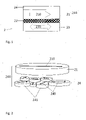
- Fig. 1 shows a TMR-based magnetic element 2 comprising a reference bilayer 244 including an antiferromagnetic layer 24 and a reference ferromagnetic layer 21 having a reference magnetization 210, wherein the antiferromagnetic layer 24 pins the reference magnetization 210 by exchange-bias.
- the magnetic element 2 further comprises a sense ferromagnetic layer 23 having a sense magnetization 230 that can be switched relative to the first magnetization 210.
- a tunnel barrier layer 22 is comprised between the reference ferromagnetic layer 21 and the sense ferromagnetic layer 23.
- the antiferromagnetic layer 24 can pin the reference magnetization 210 along a pinned direction through an exchange-bias field H ex coupling at a temperature below a threshold temperature.
- the threshold temperature can correspond to a blocking temperature, which is below the Neel temperature.
- the magnetic element 2 is not limited to a TMR- stack but can include any magnetic device such as GMR or TMR-based magnetic device including a magnetic field sensor, a magnetic random-access memory (MRAM) or a spin-torque nano-oscillator, as long as it includes a ferromagnetic layer pinning the magnetization of a ferromagnetic layer.
- MRAM magnetic random-access memory
- spin-torque nano-oscillator as long as it includes a ferromagnetic layer pinning the magnetization of a ferromagnetic layer.
- the expression "reference ferromagnetic layer” can be generalized to any ferromagnetic layer.
- the reference layer 21 can comprise one or a plurality of ferromagnetic layers or a synthetic antiferromagnet (SAF).
- the antiferromagnetic layer 24 can comprise an alloy based on manganese Mn, such as alloys based on iridium Ir and Mn (e.g., IrMn); alloys based on Fe and Mn (e.g., FeMn); alloys based on platinum Pt and Mn (e.g., PtMn); and alloys based on Ni and Mn (e.g., NiMn).
- the antiferromagnetic layer 24 comprising a metallic polycrystalline material having a grain volume distribution.
- the reference and sense layers 21, 23 can be made of a ferromagnetic material such as Fe based alloy, CoFe, NiFe or CoFeB.
- the tunnel barrier 22 can comprise an insulating material. Suitable insulating materials include oxides, such as aluminum oxide (e.g., Al 2 O 3 ) and magnesium oxide (e.g., MgO).
- a thickness of the tunnel barrier layer 22 can be in the nm range, such as from about 1 nm to about 3 nm.
- Fig. 2 represents schematically a reference ferromagnetic layer 21 and a polycrystalline antiferromagnetic layer 24 having a thickness t AF .
- the antiferromagnetic layer 24 comprises a plurality of grains 241 of various size and volume.
- Fig. 3 represents a single grain 241.
- Each grain 241 has a magnetic moment represented by the Neel vector 240 and oriented at a Neel vector angle ⁇ N .
- Uniaxial anisotropy axis 245 of each grain 241 is defined by the anisotropy angle ⁇ A .
- the reference magnetization 210 is oriented with a reference angle ⁇ FM .
- the Neel vector angle ⁇ N , anisotropy angle ⁇ A and reference angle ⁇ FM can be defined relative to a reference axis 300.
- a method to calculate performance of the magnetic element 2 comprises the steps of:
- the selected in-plane exposure magnetic fields H can be high enough to saturate the reference ferromagnetic layer 21.
- the method takes into account the different in-plane orientation of the uniaxial anisotropy axis 245 of each grain 241 of the antiferromagnetic layer 24.
- in-plane means in the plane of the layer (reference layer 21 and/or antiferromagnetic layer 24).
- the method calculates the thermal stability of exchange bias at the interface between the reference ferromagnetic layer 21 and antiferromagnetic layer 24. More particularly, the method calculates the angular deviation of exchange bias field H ex and its amplitude degradation under various conditions on external magnetic field (exposure magnetic field H), temperature (exposure temperature T), and time (exposure time ⁇ S ).
- Equation (1) K u ⁇ sin 2 ⁇ N ⁇ ⁇ A ⁇ J E t AF ⁇ cos ⁇ N ⁇ ⁇ FM
- K u is the uniaxial anisotropy constant at an anisotropy angle ⁇ A
- ⁇ is the grain's volume
- J E is the interface coupling constant
- t AF is the thickness of the antiferromagnetic layer
- ⁇ N is the Neel vector angle
- ⁇ FM is the reference angle.
- Equation (1) Energy profiles obtained from Equation (1) for different orientations of uniaxial anisotropy angle ⁇ A are shown in Fig. 4 .
- H ex H 0 ⁇ ⁇ ⁇ ⁇ f ⁇ d ⁇
- H 0 the total available exchange bias value if all grains contribute fully
- Equation (5) cannot be directly used.
- an array of grains 241 must be generated respecting the volume distribution of Equation (4) and with randomly oriented uniaxial anisotropy 245.
- the method further comprises generating an array of grains 241 using determined at least one distribution parameter.
- the array of grains 241 having a volume corresponding to the one the antiferromagnetic layer 24.
- the at least one distribution parameter can comprise mean value ⁇ and standard deviation ⁇ of the grain volume distribution function.
- all the grains 241 in the array can have a randomly oriented uniaxial anisotropy with an anisotropy angle ⁇ A between 0° and 180°.
- Equation (5) can be replaced by the summation over the contributing grains 241, i.e., the grains 241 that contribute to the exchange bias field H ex .
- the contributing grains 241 i.e., the grains 241 that contribute to the exchange bias field H ex .
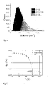
- the histogram of the volume distribution is shown comprising three regions: a first region R1 corresponding to small thermally unstable grains ( ⁇ ⁇ ⁇ 0 ) that do not contribute to exchange bias field H ex , a second region R2 corresponding to large stable grains ( ⁇ 0 > ⁇ > Q S ) that also do not contribute to the exchange bias field H ex , and a third region R3 corresponding to grains matching the condition ⁇ 0 ⁇ ⁇ ⁇ ⁇ S and responsible for the observed exchange bias H ex .
- the boundaries of the three regions R1, R2, R3 are not straight since the critical volumes ⁇ 0 and ⁇ S depend on the orientation of the anisotropy axis 245. Therefore, a summation over the grains in the second region R2 yields the value of the exchange bias field H ex .
- the method is applied to a specific reference ferromagnetic layer 21 and antiferromagnetic layer 24 and the properties of the layers 21, 24 are estimated for various exposure conditions (to an exposure magnetic field H and exposure temperature Ts). This is achieved by determining the parameters of the grain volume distribution of the polycrystalline antiferromagnetic layer 24.
- the grain volume distribution is determined by fitting experimentally measured exchange bias field H ex as a function of temperature T.
- Fig. 6 reports measured exchange bias field H ex as a function of temperature T in a sputter deposited CoFe reference ferromagnetic layer 21 and IrMn antiferromagnetic layer 24.
- the measurements were performed using a protocol similar to that described in S. Soeya, et al., J. Appl. Phys., vol. 76, no. 9, pp. 5356-5360, Nov. 1994 .
- the measurements comprise the steps of:
- Equation (2) a simplified expression for the energy barrier Equation (2) can be used setting the reference angle ⁇ FM to zero.
- the exchange bias field H ex in each i th experimental point can be calculated using Equation (7).
- ⁇ ⁇ 0 ⁇ s f ⁇ d ⁇ ⁇ 2 ⁇ ⁇ 0 ⁇ a T i f ⁇ d ⁇ H ex T i H 0 , where the critical volume at room temperature ⁇ 0 and the critical volume at setting temperature ⁇ S depend on the cooling temperature T NA , setting temperature Tset and activation period of time ⁇ act in the measurement protocol.
- ⁇ a (T i ) is the critical volume with the same form as Equation (6) but with the temperature of the i th experimental point and characteristic time ⁇ a corresponding to the exposure time of the inversed field in the protocol, and H ex (T i ) is a value of the exchange bias for the i th experimental point.
- Equation (4) Since the distribution function of Equation (4) can be easily integrated, it is possible to adjust the unknown parameters: Ho, T N , K 0 , ⁇ and ⁇ .
- T N is about 400°C for a IrMn antiferromagnetic layer.
- the "initial point” corresponds to the first experimental point in Fig. 6 , i.e., it corresponds to the exchange bias field H ex value after annealing in the high field during 90 min at 310°C.
- the parameter K 0 is about 10 6 J/m 3 ( G. Vallejo-Fernandez, et al., J. Phys. D. Appl. Phys., vol. 41, no.
- Distribution function parameters ⁇ and ⁇ can be adjusted with critical volumes defined in Equation (6) varying within acceptable ranges: 100 nm 3 ⁇ ⁇ 0 ⁇ 200 nm 3 and ⁇ S > 700 nm 3 .
- ferromagnetic layers can be separated from each other by a thin paramagnetic layer (such as Ta, Pt, Ru).
- the equilibrium angle corresponds to a minimum energy of the magnetic system.
- the exchange bias field H ex can change since some of the grains 241 may switch their state. This will lead to an additional deviation of the orientation of the reference magnetization 210 orientation (i.e., a further variation in the reference angle ⁇ FM ).
- the method comprises an iterative procedure to converge to an equilibrium magnetic state, where the equilibrium magnetic state corresponds to a minimum of energy where the exchange bias field H ex no longer rotates.
- the iterative procedure can include the steps of:
- the reference magnetization 210 magnetization direction M FM is aligned with the effective field vector corresponding to the sum of the exposure magnetic field H vector and the exchange bias field H ex vector.
- the iterative procedure can comprise an initial step aimed at setting an initial exchange bias field H ex to the reference bilayer 244 (array of grains) and corresponding to the initial measurement point.
- the initial step can comprise applying an initial exposure magnetic field H in oriented at 0° (relative to the reference axis 300) at an initial exposure temperature T in during an initial exposure time ⁇ Sin .
- the initial exposure temperature T in can be between 290°C and 310°C and the initial exposure time ⁇ Sin can be 90 min.
- the iterative procedure is repeated until convergence of the exchange bias field H ex amplitude and the exchange angle ⁇ Hex is achieved. In other words, the iterative procedure is repeated until the variation of the exchange bias field H ex amplitude and the variation of the exchange angle ⁇ Hex between two consecutive iterations is smaller than a threshold value.
- the method further comprises a release step wherein the exposure magnetic field H is removed and,the exposure temperature Ts is decreased to a release temperature T R lower than the exposure temperature Ts (for example at room temperature or 25°C), during a release time ⁇ R .
- the exchange bias field Hex amplitude and the variation of the exchange angle ⁇ Hex are partially restored towards their initial values (the values before the reference bilayer 244 was exposed to the initial exposure magnetic field H in ), corresponding to equilibrium, values of the exchange bias field H ex amplitude and the variation of the exchange angle ⁇ Hex .
- the equilibrium values of the exchange bias field H ex amplitude and the variation of the exchange angle ⁇ Hex represent the degradation of the exchange bias field H ex with the chosen exposure.
- the iterative procedure is illustrated for a specific example in Fig. 8 .
- the reference ferromagnetic layer 21 and the antiferromagnetic layer 24 are exposed, during the initial step, to an initial strong external magnetic field H in oriented at 0° (relative to the reference axis 300) at an initial exposure temperature T in between 290°C and 310°C, during an initial exposure time ⁇ Sin (for example 90 min).
- the strong external magnetic field H in is adapted to saturate the reference layer 21 in the direction of the external magnetic field H in .
- the antiferromagnetic layer 24 acquires an exchange bias field H ex having an amplitude of about 1559 Oe and oriented with an exchange angle ⁇ Hex of -0.12° (relative to the exchange angle ⁇ Hex that was set at 0° during the initial step).
- the small deviation of the exchange angle ⁇ Hex from 0° to -0.12° is due to the finite number of grains 241 in the antiferromagnetic layer 24.
- the exposure step is performed, wherein the exposure step comprises applying an exposure magnetic field H of 2 kOe at an exposure angle ⁇ H of 90° (relative to the reference axis 300) at an exposure temperature T s of 100°C and during an exposure time T s of one hour.
- the method disclosed herein can predict changes in the exchange bias field H ex for any in-plane direction of the applied exposure magnetic field H.
- the method disclosed herein can be applied to estimate the degradation of the exchange bias field H ex when subjected to a high exposure temperature Ts and an exposure magnetic field H applied at any exposure angle ⁇ H over a long period of time ⁇ .
- a high exposure temperature Ts corresponds to a temperature that is higher than the room temperature (or operating temperature).
- the method calculates the degradation of the magnetic element in conditions that go beyond the normal operational conditions.
- Fig. 9 shows an example of a temperature - time (T- ⁇ ) diagram of the reference ferromagnetic layer 21 and antiferromagnetic layer 24.
- the intensity corresponds to the variation of the reference angle ⁇ FM from an initial value of 0°, after applying an external magnetic field H of 2 kOe at an exposure angle ⁇ H of 90°. Time intervals of one and ten years are indicated by the vertical lines.
- the iterative procedure comprising the release step is applied for each T and ⁇ point.
- the diagram reflects the thermal stability of the reference ferromagnetic layer 21 and antiferromagnetic layer 24.
- the diagram can be used to predict the longterm degradation of the exchange bias field H ex and, therefore, the reduction of accuracy and performance for the magnetic element 2.
- the method comprises, at each iteration, calculating an average variation of the exchange bias field H ex amplitude and of the exchange angle ⁇ Hex by finding an equilibrium state of the reference bilayer 244 by using a statistical Metropolis-Hastings algorithm; adjusting the reference angle ⁇ FM according to the calculated average variation of the exchange bias field H ex amplitude and of the exchange angle ⁇ Hex .
- calculating an average variation of the exchange bias field H ex amplitude and of the exchange angle ⁇ Hex can comprise:
- each grain 241 has a low and high energy minimum of the Neel vector.
- setting the energy state of each grain 241 can comprise:
- the method disclosed herein can further be applied to the case where the reference layer 21 is non-uniformly magnetized.
- the reference layer 21 may be divided in a plurality of areas (not shown) where the reference magnetization 210 is considered substantially uniform in each area.
- antiferromagnetic grain's energy will depend on a local area magnetization of the reference layer 21.
- calculating the reference angle ⁇ FM can comprise performing micromagnetic computation procedure of the whole reference layer (210) including all single-domains areas.
- the present disclosure further concerns a computer program product comprising instructions which, when the program is executed by a computer, cause the computer to carry out the method.
Landscapes
- Physics & Mathematics (AREA)
- Condensed Matter Physics & Semiconductors (AREA)
- General Physics & Mathematics (AREA)
- Engineering & Computer Science (AREA)
- Chemical & Material Sciences (AREA)
- Crystallography & Structural Chemistry (AREA)
- Power Engineering (AREA)
- Computer Hardware Design (AREA)
- Magnetic Heads (AREA)
- Hall/Mr Elements (AREA)
- Measuring Magnetic Variables (AREA)
Abstract
Description
- The present invention concerns methods for determining degradation dependencies of electrical and magnetic parameters in magnetic elements, such as magnetic sensors.
- GMR or TMR-based magnetic devices such as magnetic field sensors, magnetic random-access memory (MRAM) or spin-torque nanooscillators often comprise a ferromagnetic layer exchange coupled to an antiferromagnetic layer. The phenomenon of exchange bias, which occurs due to the exchange coupling between the ferromagnetic layer and the antiferromagnetic layer, makes it possible to improve the stability of the magnetic device.
- Thermal stability within the antiferromagnetic layer is a key parameter to achieve a working magnetic device. During typical operation, the magnetic device may be exposed to strong magnetic fields and high temperatures. Thermal relaxation effects during such exposure can result in shifts in the magnetic device properties. It is therefore important to predict the expected degradation of the magnetic device under specific exposure conditions.
- Various models have been proposed to estimate the thermal stability of exchange bias in the ferromagnetic and antiferromagnetic layers, based on the polycrystalline antiferromagnetic layer structure and thermal fluctuations (see for example: G Vallejo-Fernandez et al 2008, J. Phys. D: Appl. Phys. 41 112001). In these models, the grain anisotropy axis of the polycrystalline antiferromagnetic layer is assumed to be oriented in only one direction such that the free energy of each grain does not depend on the direction of the ferromagnetic layer magnetization. It is not possible in this case to properly account for the effect of angular variation of an external magnetic field applied on the ferromagnetic and antiferromagnetic layers.
- The present disclosure concerns a method to determine degradation dependencies of electrical and magnetic parameters in TMR magnetic field sensor under accelerated lifetime test (ALT). The method calculates deviations (degradation) over time of initial exchange bias direction and strength due to high temperature and/or magnetic field. It is then possible to estimate the effect on final output parameters of a TMR sensor (linearity, angular error, sensitivity, offset etc.). The method is based on the polycrystalline model of antiferromagnet and Arrhenius's concept of thermal activation energy using a novel self-consistent recursion procedure.
- According to an embodiment, a method to calculate performance of a magnetic element comprising a reference bilayer including a ferromagnetic reference layer having a reference magnetization and an antiferromagnetic layer pining the reference magnetization by exchange-bias, the antiferromagnetic layer comprising a metallic polycrystalline material having a grain volume distribution; the method comprising: measuring an exchange-bias field of the antiferromagnetic layer at selected exposure temperatures, under selected in-plane exposure magnetic fields and exposure time applied to the reference bilayer; fitting a grain volume distribution function to the measured exchange-bias fields to determine at least one distribution parameter characterizing the volume distribution of the grains and at least one magnetic parameter characterizing the magnetic properties of the antiferromagnetic layer; calculating a reference angle corresponding to an in-plane variation in the direction of the reference magnetization, as a function of a direction of the exposure magnetic field; and calculating the exchange bias field for any value of the in-plane exposure magnetic field, exposure temperature and exposure time, using the calculated reference angle and determined said at least one distribution and magnetic parameters in the grain volume distribution function.
- The present disclosure further concerns a computer program product comprising instructions which, when the program is executed by a computer, cause the computer to carry out the method.
- The method disclosed herein can predict the properties of a magnetic element, such as a magnetic sensor, including sensitivity, linearity, and angular error over time under ALT test. The properties can be predicted rapidly and in both short and long-time term working conditions, therefore allowing estimating the lifetime of the magnetic element with given specifications. In particular, the properties can be predicted over a longer time interval (years) than ALT measurements (hours) and therefore improve prediction of a full lifetime period.
- The method can be applied to any magnetic elements comprising spintronic devices based on antiferromagnet/ferromagnet interface with exchange bias pinning, such as (MRAM, field sensors, spin-torque nanooscillators, under different exposure conditions such as magnetic field, temperature and time. The method takes into account the different in-plane orientation of the uniaxial anisotropy of each grain of the antiferromagnetic layer. The method can therefore contribute, together with specific device models and usage cases, to evaluating potential lifetime performance shifts in such magnetic elements.
- Exemplar embodiments of the invention are disclosed in the description and illustrated by the drawings in which:
-
Fig. 1 illustrates schematically a TMR-based magnetic element comprising a reference bilayer including a reference ferromagnetic layer and an antiferromagnetic layer; -
Fig. 2 represents schematically a reference ferromagnetic layer and a polycrystalline antiferromagnetic layer; -
Fig. 3 represents a single grain of the polycrystalline antiferromagnetic layer; -
Fig. 4 reports energy profiles for different orientations of uniaxial anisotropy angle of a grain; -
Fig. 5 shows a histogram of a volume distribution of the grains; -
Fig. 6 reports measured exchange bias field as a function of temperature in a sputter-deposited CoFe reference ferromagnetic layer and IrMn antiferromagnetic layer; -
Fig. 7 illustrates an iterative procedure to converge to a magnetic state of the reference bilayer; -
Fig. 8 shows the results of the iterative procedure for a specific example; -
Fig. 9 shows an example of a temperature versus time diagram of the reference bilayer. -
Fig. 1 shows a TMR-basedmagnetic element 2 comprising areference bilayer 244 including anantiferromagnetic layer 24 and a referenceferromagnetic layer 21 having areference magnetization 210, wherein theantiferromagnetic layer 24 pins thereference magnetization 210 by exchange-bias. Themagnetic element 2 further comprises a senseferromagnetic layer 23 having asense magnetization 230 that can be switched relative to thefirst magnetization 210. Atunnel barrier layer 22 is comprised between the referenceferromagnetic layer 21 and the senseferromagnetic layer 23. Theantiferromagnetic layer 24 can pin thereference magnetization 210 along a pinned direction through an exchange-bias field Hex coupling at a temperature below a threshold temperature. The threshold temperature can correspond to a blocking temperature, which is below the Neel temperature. Themagnetic element 2 is not limited to a TMR- stack but can include any magnetic device such as GMR or TMR-based magnetic device including a magnetic field sensor, a magnetic random-access memory (MRAM) or a spin-torque nano-oscillator, as long as it includes a ferromagnetic layer pinning the magnetization of a ferromagnetic layer. Moreover, the expression "reference ferromagnetic layer" can be generalized to any ferromagnetic layer. - The
reference layer 21 can comprise one or a plurality of ferromagnetic layers or a synthetic antiferromagnet (SAF). Theantiferromagnetic layer 24 can comprise an alloy based on manganese Mn, such as alloys based on iridium Ir and Mn (e.g., IrMn); alloys based on Fe and Mn (e.g., FeMn); alloys based on platinum Pt and Mn (e.g., PtMn); and alloys based on Ni and Mn (e.g., NiMn). Theantiferromagnetic layer 24 comprising a metallic polycrystalline material having a grain volume distribution. - The reference and
sense layers tunnel barrier 22 can comprise an insulating material. Suitable insulating materials include oxides, such as aluminum oxide (e.g., Al2O3) and magnesium oxide (e.g., MgO). A thickness of thetunnel barrier layer 22 can be in the nm range, such as from about 1 nm to about 3 nm. -
Fig. 2 represents schematically a referenceferromagnetic layer 21 and a polycrystallineantiferromagnetic layer 24 having a thickness tAF. Theantiferromagnetic layer 24 comprises a plurality ofgrains 241 of various size and volume.Fig. 3 represents asingle grain 241. Eachgrain 241 has a magnetic moment represented by the Neelvector 240 and oriented at a Neel vector angle θN. Uniaxialanisotropy axis 245 of eachgrain 241 is defined by the anisotropy angle θA. At the interface between theantiferromagnetic layer 24 and the referenceferromagnetic layer 21, thegrains 241 are coupled with the referenceferromagnetic layer 21, which is uniformly magnetized. Thereference magnetization 210 is oriented with a reference angle θFM. The Neel vector angle θN, anisotropy angle θA and reference angle θFM can be defined relative to areference axis 300. - In an embodiment, a method to calculate performance of the
magnetic element 2 comprises the steps of: - measuring an exchange-bias field Hex of the
antiferromagnetic layer 24 at selected exposure temperatures Ts, under selected in-plane exposure magnetic fields H applied to thereference bilayer 244, during an exposure time τs; - fitting a grain volume distribution function to the measured exchange-bias fields Hex to determine at least one distribution parameter characterizing the volume distribution of the grains and at least one magnetic parameter characterizing the magnetic properties of the
antiferromagnetic layer 24; - calculating a reference angle θFM corresponding to an in-plane variation in the direction of the
reference magnetization 210, as a function of a direction of the exposure magnetic field H; and - calculating the exchange bias field Hex for any value (amplitude and direction) of the in-plane exposure magnetic field H, exposure temperature TS and exposure time τS, using the calculated reference angle θFM and determined said at least one distribution and magnetic parameters in the grain volume distribution function.
- The selected in-plane exposure magnetic fields H can be high enough to saturate the reference
ferromagnetic layer 21. The method takes into account the different in-plane orientation of theuniaxial anisotropy axis 245 of eachgrain 241 of theantiferromagnetic layer 24. Here, the expression "in-plane" means in the plane of the layer (reference layer 21 and/or antiferromagnetic layer 24). - The method calculates the thermal stability of exchange bias at the interface between the reference
ferromagnetic layer 21 andantiferromagnetic layer 24. More particularly, the method calculates the angular deviation of exchange bias field Hex and its amplitude degradation under various conditions on external magnetic field (exposure magnetic field H), temperature (exposure temperature T), and time (exposure time τS). - The total energy E of an antiferromagnetic grain shown in
Fig. 1 is given by the Equation (1):
- where Ku is the uniaxial anisotropy constant at an anisotropy angle·θA, Ω is the grain's volume, JE is the interface coupling constant, tAF is the thickness of the
antiferromagnetic layer 24, θN is the Neel vector angle, and θFM is the reference angle. - Energy profiles obtained from Equation (1) for different orientations of uniaxial anisotropy angle θA are shown in
Fig. 4 . The energy barriers between two metastable states of agrain 241 can be calculated from the derivative of Equation (1). If the anisotropy angle θA is equal to zero, the approximate expression for the barriers ΔE+ and ΔE- reduces to Equation (2):
- The corresponding time τ± for a grain to overcome the energy barrier ΔE± during thermal fluctuations is given by the Neel-Arrhenius law Equation (3):

- Temperature dependence of the anisotropy constant K0 and interface exchange energy Jo at 0°K follow the power law Ku = K0 (1-T/TN), JE = Jo (1-T/TN)0.33, where TN is the Neel temperature of the
antiferromagnetic layer 24. - The grain volume distribution function is assumed to follow a lognormal function such as in Equation (4):

- Where σ is the standard deviation and µ is the mean value. Assuming that the
reference bilayer 244 is exposed to external disturbances over time (for example, annealing at elevated temperatures followed by cooling in a magnetic field) which change the energy of thegrains 241. The resulting exchange bias field Hex can be calculated using Equation (5):
grains 241 that satisfy the condition, where Ω0 < Ω < ΩS, where:
- Since in the present method a random direction of the anisotropy in the
grains 241 is considered, Equation (5) cannot be directly used. To simulate the referenceferromagnetic layer 21 and theantiferromagnetic layer 24, an array ofgrains 241 must be generated respecting the volume distribution of Equation (4) and with randomly orienteduniaxial anisotropy 245. - In an embodiment, the method further comprises generating an array of
grains 241 using determined at least one distribution parameter. The array ofgrains 241 having a volume corresponding to the one theantiferromagnetic layer 24. The at least one distribution parameter can comprise mean value µ and standard deviation σ of the grain volume distribution function. - In an example, all the
grains 241 in the array can have a randomly oriented uniaxial anisotropy with an anisotropy angle θA between 0° and 180°. The lognormal distribution was calculated the mean value µ = 6.28 and the standard deviation σ = 0.52. - To calculate the resulting exchange bias field Hex after exposure (to an exposure magnetic field H and exposure temperature Ts), Equation (5) can be replaced by the summation over the contributing
grains 241, i.e., thegrains 241 that contribute to the exchange bias field Hex. InFig. 5 , the histogram of the volume distribution is shown comprising three regions: a first region R1 corresponding to small thermally unstable grains (Ω < Ω0) that do not contribute to exchange bias field Hex, a second region R2 corresponding to large stable grains (Ω0 > Ω > QS) that also do not contribute to the exchange bias field Hex, and a third region R3 corresponding to grains matching the condition Ω0 < Ω < ΩS and responsible for the observed exchange bias Hex. The boundaries of the three regions R1, R2, R3 are not straight since the critical volumes Ω0 and ΩS depend on the orientation of theanisotropy axis 245. Therefore, a summation over the grains in the second region R2 yields the value of the exchange bias field Hex. - In an embodiment, the method is applied to a specific reference
ferromagnetic layer 21 andantiferromagnetic layer 24 and the properties of thelayers antiferromagnetic layer 24. - In one aspect, the grain volume distribution is determined by fitting experimentally measured exchange bias field Hex as a function of temperature T.
-
Fig. 6 reports measured exchange bias field Hex as a function of temperature T in a sputter deposited CoFe referenceferromagnetic layer 21 and IrMnantiferromagnetic layer 24. The measurements were performed using a protocol similar to that described in S. Soeya, et al., J. Appl. Phys., vol. 76, no. 9, pp. 5356-5360, Nov. 1994. In particular, the measurements comprise the steps of: - heating the
reference bilayer 244 to a setting temperature Tset which does not result in interfacial diffusion, with a saturating magnetic field sufficient to saturate theantiferromagnetic layer 24 in the direction of the layer easy axis; - cooling the
reference bilayer 244 to a cooling temperature TNA where no thermal activation occurs; - reversing the polarity of the saturating magnetic field;
- heating the
reference bilayer 244 to an activation temperature Tact where thermal activation occurs; - cooling the
reference bilayer 244 to a cooling temperature TNA; - wait for an activation period of time τact and
- measure a hysteresis loop. The exchange bias field Hex being obtained from the shift of the hysteresis loop relative to the zero-field position.
- Since there are only two opposite field directions used in the experiment, a simplified expression for the energy barrier Equation (2) can be used setting the reference angle θFM to zero. Using the explicit expression for the lognormal distribution of Equation (4) and its integral, the exchange bias field Hex in each ith experimental point can be calculated using Equation (7).

- Since the distribution function of Equation (4) can be easily integrated, it is possible to adjust the unknown parameters: Ho, TN, K0, σ and µ. Note that parameter Ho is close but slightly larger than the initial measurement point at room temperature, TN is about 400°C for a IrMn antiferromagnetic layer. Here, the "initial point" corresponds to the first experimental point in
Fig. 6 , i.e., it corresponds to the exchange bias field Hex value after annealing in the high field during 90 min at 310°C. The parameter K0 is about 106 J/m3 (G. Vallejo-Fernandez, et al., J. Phys. D. Appl. Phys., vol. 41, no. 11, p. 112001). Distribution function parameters σ and µ can be adjusted with critical volumes defined in Equation (6) varying within acceptable ranges: 100 nm3 < Ω0 < 200 nm3 and ΩS > 700 nm3. - After the above parameters H0, TN, K0, σ and µ have been determined, it is possible to simulate the evolution of the exchange bias field Hex under specific exposure conditions including exposure temperature Ts, exposure magnetic field H, and exposure time τS. Applying an in-plane exposure magnetic field H to the reference
ferromagnetic layer 21 and IrMnantiferromagnetic layer 24 at a certain exposure angle θH relative to thereference axis 300 leads to a deviation of the orientation of the reference magnetization 210 (i.e., a variation in the reference angle θFM). If one considers thereference magnetization 210 to be uniform (in the macrospin approximation), its direction will be aligned with the effective field, where the effective field is the sum of the external magnetic field H and the exchange bias field Hex. - For a
reference bilayer 244 comprising more than one reference ferromagnetic layer, it is necessary to use some numerical methods such as the Landau-Lifshitz-Gilbert equation to find the equilibrium angle. The ferromagnetic layers can be separated from each other by a thin paramagnetic layer (such as Ta, Pt, Ru). The equilibrium angle corresponds to a minimum energy of the magnetic system. - When the
reference magnetization 210 orientation deviates from its initial direction (i.e., when there is a variation in the reference angle θFM), the exchange bias field Hex can change since some of thegrains 241 may switch their state. This will lead to an additional deviation of the orientation of thereference magnetization 210 orientation (i.e., a further variation in the reference angle θFM). - In one aspect illustrated in
Fig. 7 , the method comprises an iterative procedure to converge to an equilibrium magnetic state, where the equilibrium magnetic state corresponds to a minimum of energy where the exchange bias field Hex no longer rotates. The iterative procedure can include the steps of: - Performing an exposure step comprising applying an in-plane exposure magnetic field H oriented at an exposure angle θH (relative to the reference axis 300), at an exposure temperature Ts and during an exposure time τS;
- calculating the reference angle θFM of the
reference magnetization 210 direction MFM; and - calculating the variation of the exchange bias field Hex amplitude and the variation of the exchange angle θHex.
- The
reference magnetization 210 magnetization direction MFM is aligned with the effective field vector corresponding to the sum of the exposure magnetic field H vector and the exchange bias field Hex vector. - The iterative procedure can comprise an initial step aimed at setting an initial exchange bias field Hex to the reference bilayer 244 (array of grains) and corresponding to the initial measurement point. The initial step can comprise applying an initial exposure magnetic field Hin oriented at 0° (relative to the reference axis 300) at an initial exposure temperature Tin during an initial exposure time τSin. Here, the initial exposure temperature Tin can be between 290°C and 310°C and the initial exposure time τSin can be 90 min.
- The iterative procedure is repeated until convergence of the exchange bias field Hex amplitude and the exchange angle θHex is achieved. In other words, the iterative procedure is repeated until the variation of the exchange bias field Hex amplitude and the variation of the exchange angle θHex between two consecutive iterations is smaller than a threshold value.
- In one aspect, the method further comprises a release step wherein the exposure magnetic field H is removed and,the exposure temperature Ts is decreased to a release temperature TR lower than the exposure temperature Ts (for example at room temperature or 25°C), during a release time τR. During the release time τR, the exchange bias field Hex amplitude and the variation of the exchange angle θHex are partially restored towards their initial values (the values before the
reference bilayer 244 was exposed to the initial exposure magnetic field Hin), corresponding to equilibrium, values of the exchange bias field Hex amplitude and the variation of the exchange angle θHex. The equilibrium values of the exchange bias field Hex amplitude and the variation of the exchange angle θHex represent the degradation of the exchange bias field Hex with the chosen exposure. - The iterative procedure is illustrated for a specific example in
Fig. 8 . In this example, the referenceferromagnetic layer 21 and theantiferromagnetic layer 24 are exposed, during the initial step, to an initial strong external magnetic field Hin oriented at 0° (relative to the reference axis 300) at an initial exposure temperature Tin between 290°C and 310°C, during an initial exposure time τSin (for example 90 min). The strong external magnetic field Hin is adapted to saturate thereference layer 21 in the direction of the external magnetic field Hin. Theantiferromagnetic layer 24 acquires an exchange bias field Hex having an amplitude of about 1559 Oe and oriented with an exchange angle θHex of -0.12° (relative to the exchange angle θHex that was set at 0° during the initial step). The small deviation of the exchange angle θHex from 0° to -0.12° is due to the finite number ofgrains 241 in theantiferromagnetic layer 24. Then, the exposure step is performed, wherein the exposure step comprises applying an exposure magnetic field H of 2 kOe at an exposure angle θH of 90° (relative to the reference axis 300) at an exposure temperature Ts of 100°C and during an exposure time Ts of one hour. In this example, iterating 10 times the exposure step was sufficient to achieve convergence. After convergence, the variation of the exchange angle θHex reaches 3° and the variation of the exchange bias field Hex amplitude is -55 Oe. After performing the release step, the variation of the equilibrium values of exchange angle θHex reaches about 0.58° and the variation of the exchange bias field Hex amplitude is about 35 Oe. - The method disclosed herein can predict changes in the exchange bias field Hex for any in-plane direction of the applied exposure magnetic field H.
- The method disclosed herein can be applied to estimate the degradation of the exchange bias field Hex when subjected to a high exposure temperature Ts and an exposure magnetic field H applied at any exposure angle θH over a long period of time τ. Here, a high exposure temperature Ts corresponds to a temperature that is higher than the room temperature (or operating temperature). Indeed, the method calculates the degradation of the magnetic element in conditions that go beyond the normal operational conditions.
-
Fig. 9 shows an example of a temperature - time (T-τ) diagram of the referenceferromagnetic layer 21 andantiferromagnetic layer 24. The intensity corresponds to the variation of the reference angle θFM from an initial value of 0°, after applying an external magnetic field H of 2 kOe at an exposure angle θH of 90°. Time intervals of one and ten years are indicated by the vertical lines. The iterative procedure comprising the release step is applied for each T and τ point. The diagram reflects the thermal stability of the referenceferromagnetic layer 21 andantiferromagnetic layer 24. The diagram can be used to predict the longterm degradation of the exchange bias field Hex and, therefore, the reduction of accuracy and performance for themagnetic element 2. - In an alternative embodiment, the method comprises, at each iteration, calculating an average variation of the exchange bias field Hex amplitude and of the exchange angle θHex by finding an equilibrium state of the
reference bilayer 244 by using a statistical Metropolis-Hastings algorithm; adjusting the reference angle θFM according to the calculated average variation of the exchange bias field Hex amplitude and of the exchange angle θHex. - In one aspect, calculating an average variation of the exchange bias field Hex amplitude and of the exchange angle θHex can comprise:
- setting the energy state of each
grain 241; - calculating an average variation of the exchange bias field Hex amplitude and of the exchange angle θHex; and
- aligning the
reference magnetization 210 with calculated exchange angle θHex. - In one aspect, each
grain 241 has a low and high energy minimum of the Neel vector. Here, setting the energy state of eachgrain 241 can comprise: - calculating a low lifetime τ- for the low energy minimum and a high lifetime τ+ for the high energy minimum;
- estimate the current lifetime τ of the current energy state of the
grain 241 - if the determined current switching lifetime τ is larger than the low lifetime τ- and smaller than the high lifetime τ+, setting the
grain 241 to the low energy minimum; - if the determined lifetime τ is smaller than the low lifetime τ-, do not change the energy of the
grain 241; and - if the determined current lifetime τ is larger than the high lifetime τ+, setting the
grain 241 to any of two low or high energy minimum with 50% probability. - The method disclosed herein can further be applied to the case where the
reference layer 21 is non-uniformly magnetized. In such case, thereference layer 21 may be divided in a plurality of areas (not shown) where thereference magnetization 210 is considered substantially uniform in each area. In this case, antiferromagnetic grain's energy will depend on a local area magnetization of thereference layer 21. In the iterative procedure, calculating the reference angle θFM can comprise performing micromagnetic computation procedure of the whole reference layer (210) including all single-domains areas. - The present disclosure further concerns a computer program product comprising instructions which, when the program is executed by a computer, cause the computer to carry out the method.
-
- 2
- magnetic element
- 21
- reference layer
- 210
- reference magnetization
- 23
- sense layer
- 230
- sense magnetization
- 24
- antiferromagnetic layer
- 240
- magnetic moment, Néel vector
- 241
- grain
- 244
- reference bilayer
- 245
- uniaxial anisotropy axis
- 300
- reference axis
- Ω
- grain volume
- Ω0
- critical volume at room temperature
- ΩS
- critical volume at setting temperature
- θA
- anisotropy angle
- θH
- exposure angle
- θHex
- exchange angle
- θN
- Neel vector angle
- θFM
- reference angle
- τ
- period of time
- τC
- time elapsed after exposure
- TR
- release time
- τS
- exposure time
- τSin
- initial exposure time
- H
- exposure magnetic field
- Hex
- exchange bias field
- Hin
- initial exposure magnetic field
- J0
- interface coupling constant at 0K
- JE
- interface coupling constant
- K0
- anisotropy constant at 0K
- Ku
- uniaxial anisotropy constant
- MFM
- magnetization direction of reference layer
- σ
- standard deviation
- tAF
- thickness of the antiferromagnetic layer
- T
- temperature
- T0
- room temperature
- Tact
- activation temperature
- Tin
- initial exposure temperature
- TNA
- cooling temperature
- TR
- release temperature
- TS
- exposure temperature
- Tset
- setting temperature
- µ
- mean value
Claims (13)
- Method to calculate performance of a magnetic element (2) comprising a reference bilayer (244) including a ferromagnetic reference layer (21) having a reference magnetization (210) and an antiferromagnetic layer (24) pining the reference magnetization (210) by exchange-bias, the antiferromagnetic layer (24) comprising a metallic polycrystalline material having a grain volume distribution; the method comprising:measuring an exchange-bias field (Hex) of the.antiferromagnetic layer (24) at selected exposure temperatures (Ts), under selected in-plane exposure magnetic fields (H) applied to the reference bilayer (244), during an exposure time (τS);fitting a grain volume distribution function to the measured exchange-bias fields (Hex) to determine at least one distribution parameter characterizing the volume distribution of the grains and at least one magnetic parameter characterizing the magnetic properties of the antiferromagnetic layer (24);calculating a reference angle (θFM) corresponding to an in-plane variation in the direction of the reference magnetization (210), as a function of a direction of the exposure magnetic field (H);calculating the exchange bias field (Hex) for any value of the in-plane exposure magnetic field (H), exposure temperature (Ts) and exposure time (τS), using the calculated reference angle (θFM) and determined said at least one distribution and magnetic parameters in the grain volume distribution function.
- The method according to claim 1,
further comprising generating an array of grains (241) using determined said at least one distribution parameter, the array of grains (241) having a volume corresponding to the one the antiferromagnetic layer (24). - The method according claim 2,
wherein each grain has a randomly oriented uniaxial anisotropy (Ku). - The method according to any one of claims 1 to 3,
wherein said at least one distribution parameter comprises mean value (µ) and standard deviation (σ). - The method according to any one of claims 1 to 4,
wherein calculating the exchange bias field (Hex) comprises using determined said at least one magnetic parameter in the grain volume distribution function to calculate the grains volumes that contribute to the exchange-bias filed (Hex). - The method according to any one of claims 1 to 5,
wherein said at least one magnetic parameter comprises uniaxial anisotropy constant (K0), maximum exchange bias field (Hex0) and Neel temperature (TN) of the antiferromagnetic layer (24). - The method according to claim 5 or 6,
comprising integrating the grain volume distribution function for the grains volumes that contribute to the exchange-bias filed (Hex). - The method according to any one of claims 1 to 7,
wherein the grain volume distribution function is a lognormal function. - The method according to any one of claims 1 to 8,
wherein the steps of calculating a reference angle (θFM) and calculating the exchange bias field (Hex) comprises an iterative procedure including:calculating the reference angle (θFM) for an exposure magnetic field (H) oriented at a given exposure angle (θH); andcalculating a variation of the exchange bias field (Hex) amplitude and of the exchange angle (θHex);wherein the iterative procedure is repeated until the variation of the exchange bias field (Hex) amplitude and of the exchange angle (θHex) between two consecutive iterations is smaller than a threshold value. - The method according to claims 2 and 9,
comprises, at each iteration, calculating an average variation of the exchange bias field (Hex) amplitude and of the exchange angle (θHex) by finding an equilibrium state of the reference bilayer (244) by using a statistical Metropolis-Hastings algorithm; and
adjusting the reference angle (θFM) according to the calculated average variation of the exchange bias field (Hex) amplitude and of the exchange angle (θHex). - The method according to claim 10,
wherein calculating an average variation of the exchange bias field (Hex) amplitude and of the exchange angle (θHex) comprises:setting the energy state of each grain (241);calculating an average variation of the exchange bias field (Hex) amplitude and of the exchange angle (θHex); andaligning the reference magnetization (210) with calculated exchange angle (θHex). - The method according to claim 11,
wherein each grain (241) has a low and high energy minimum of the Neel vector; wherein setting the energy state of each grain (241) comprises:calculating a low switching time (τ-) for the low energy minimum and a high switching time (τ+) for the high energy minimum;determining a switching time (τ) of the grain (241);if the determined switching time τ is larger than the low switching time (τ) and smaller than the high switching time (τ+), setting the grain (241) to the low energy minimum;if the determined switching time (τ) is smaller than the low switching time (τ-), do not change the energy of the grain (241);if the determined switching time (τ) is larger than the high switching time (τ+), setting the grain (241) to any of two low or high energy minimum with 50% probability. - A computer program product comprising instructions which, when the program is executed by a computer, cause the computer to carry out the method according to claims 1 to 12.
Priority Applications (5)
| Application Number | Priority Date | Filing Date | Title |
|---|---|---|---|
| EP21315065.9A EP4075435B8 (en) | 2021-04-13 | 2021-04-13 | Method to calculate performance of a magnetic element comprising a ferromagnetic layer exchange-coupled to an antiferromagnetic layer |
| KR1020237038371A KR20230169220A (en) | 2021-04-13 | 2022-04-04 | Method for calculating the performance of a magnetic device containing an antiferromagnetic layer and an exchange-coupled ferromagnetic layer |
| JP2023562726A JP7833483B2 (en) | 2021-04-13 | 2022-04-04 | Performance calculation method for a magnetic element having a ferromagnetic layer exchanged-coupled to an antiferromagnetic layer. |
| US18/555,075 US20240210498A1 (en) | 2021-04-13 | 2022-04-04 | Method to calculate performance of a magnetic element comprising a ferromagnetic layer exchange-coupled to an antiferromagnetic layer |
| PCT/IB2022/053104 WO2022219454A1 (en) | 2021-04-13 | 2022-04-04 | Method to calculate performance of a magnetic element comprising a ferromagnetic layer exchange-coupled to an antiferromagnetic layer |
Applications Claiming Priority (1)
| Application Number | Priority Date | Filing Date | Title |
|---|---|---|---|
| EP21315065.9A EP4075435B8 (en) | 2021-04-13 | 2021-04-13 | Method to calculate performance of a magnetic element comprising a ferromagnetic layer exchange-coupled to an antiferromagnetic layer |
Publications (3)
| Publication Number | Publication Date |
|---|---|
| EP4075435A1 true EP4075435A1 (en) | 2022-10-19 |
| EP4075435B1 EP4075435B1 (en) | 2024-03-06 |
| EP4075435B8 EP4075435B8 (en) | 2024-04-10 |
Family
ID=75825775
Family Applications (1)
| Application Number | Title | Priority Date | Filing Date |
|---|---|---|---|
| EP21315065.9A Active EP4075435B8 (en) | 2021-04-13 | 2021-04-13 | Method to calculate performance of a magnetic element comprising a ferromagnetic layer exchange-coupled to an antiferromagnetic layer |
Country Status (5)
| Country | Link |
|---|---|
| US (1) | US20240210498A1 (en) |
| EP (1) | EP4075435B8 (en) |
| JP (1) | JP7833483B2 (en) |
| KR (1) | KR20230169220A (en) |
| WO (1) | WO2022219454A1 (en) |
Citations (1)
| Publication number | Priority date | Publication date | Assignee | Title |
|---|---|---|---|---|
| US20140334032A1 (en) * | 2013-05-13 | 2014-11-13 | HGST Netherlands B.V. | Antiferromagnetic (afm) grain growth controlled random telegraph noise (rtn) suppressed magnetic head |
Family Cites Families (3)
| Publication number | Priority date | Publication date | Assignee | Title |
|---|---|---|---|---|
| US7738220B1 (en) * | 1998-06-30 | 2010-06-15 | Kabushiki Kaisha Toshiba | Magnetoresistance effect element, magnetic head, magnetic head assembly, magnetic storage system |
| KR101093776B1 (en) * | 2010-01-21 | 2011-12-19 | 충남대학교산학협력단 | Magnetic sensor |
| WO2019171660A1 (en) * | 2018-03-07 | 2019-09-12 | 住友重機械工業株式会社 | Magnetic field analysis device, analysis method, and program |
-
2021
- 2021-04-13 EP EP21315065.9A patent/EP4075435B8/en active Active
-
2022
- 2022-04-04 US US18/555,075 patent/US20240210498A1/en active Pending
- 2022-04-04 WO PCT/IB2022/053104 patent/WO2022219454A1/en not_active Ceased
- 2022-04-04 KR KR1020237038371A patent/KR20230169220A/en active Pending
- 2022-04-04 JP JP2023562726A patent/JP7833483B2/en active Active
Patent Citations (1)
| Publication number | Priority date | Publication date | Assignee | Title |
|---|---|---|---|---|
| US20140334032A1 (en) * | 2013-05-13 | 2014-11-13 | HGST Netherlands B.V. | Antiferromagnetic (afm) grain growth controlled random telegraph noise (rtn) suppressed magnetic head |
Non-Patent Citations (4)
| Title |
|---|
| G VALLEJO-FERNANDEZ ET AL., J. PHYS. D: APPL. PHYS., vol. 41, 2008, pages 112001 |
| G. VALLEJO-FERNANDEZ ET AL., J. PHYS. D. APPL. PHYS., vol. 41, no. 11, pages 112001 |
| OGRADY K ET AL: "A new paradigm for exchange bias in polycrystalline thin films", JOURNAL OF MAGNETISM AND MAGNETIC MATERIALS, ELSEVIER, AMSTERDAM, NL, vol. 322, no. 8, 1 April 2010 (2010-04-01), pages 883 - 899, XP026882925, ISSN: 0304-8853, [retrieved on 20091216], DOI: 10.1016/J.JMMM.2009.12.011 * |
| S. SOEYA ET AL., J. APPL. PHYS., vol. 76, no. 9, November 1994 (1994-11-01), pages 5356 - 5360 |
Also Published As
| Publication number | Publication date |
|---|---|
| EP4075435B8 (en) | 2024-04-10 |
| US20240210498A1 (en) | 2024-06-27 |
| WO2022219454A1 (en) | 2022-10-20 |
| JP2024517385A (en) | 2024-04-22 |
| KR20230169220A (en) | 2023-12-15 |
| EP4075435B1 (en) | 2024-03-06 |
| JP7833483B2 (en) | 2026-03-19 |
Similar Documents
| Publication | Publication Date | Title |
|---|---|---|
| Tsang et al. | Temperature dependence of unidirectional anisotropy effects in the Permalloy‐FeMn systems | |
| US9236103B2 (en) | Bipolar spin-transfer switching | |
| EP1825285B1 (en) | A method and apparatus for magnetic field measurements using a magnetoresistive sensor | |
| Lee et al. | Design consideration of magnetic tunnel junctions for reliable high-temperature operation of STT-MRAM | |
| Urazhdin et al. | Noncollinear spin transport in magnetic multilayers | |
| JP2006527497A (en) | Method for manufacturing a device comprising a magnetic layer structure | |
| US20220350572A1 (en) | Random number generation unit and computing system | |
| Paranjape et al. | Nonlinear electrical transport through artificial grain-boundary junctions in La 0.7 Ca 0.3 MnO 3 epitaxial thin films | |
| JP3334599B2 (en) | Method and apparatus for measuring magnetization direction of magnetoresistive element | |
| Böhnert et al. | Magnetic tunnel junctions with integrated thermometers for magnetothermopower measurements | |
| US6794862B2 (en) | Magnetic thin film sensor based on the extraordinary hall effect | |
| EP4075435B1 (en) | Method to calculate performance of a magnetic element comprising a ferromagnetic layer exchange-coupled to an antiferromagnetic layer | |
| US9753100B2 (en) | Magnetic sensor | |
| Van Beek et al. | Four point probe ramped voltage stress as an efficient method to understand breakdown of STT-MRAM MgO tunnel junctions | |
| Le Gall et al. | Effect of spin transfer torque on domain wall motion regimes in [Co/Ni] superlattice wires | |
| Theeuwen et al. | Nanoconstriction microscopy of the giant magnetoresistance in cobalt/copper spin valves | |
| Van Beek et al. | Voltage acceleration and pulse dependence of barrier breakdown in MgO based magnetic tunnel junctions | |
| KR102813503B1 (en) | Method for measuring external magnetic field using at least one magnetic memory point | |
| Van Beek et al. | Impact of SOT & STT stress on MTJ degradation in SOT-MRAM | |
| Tamaru et al. | Experimental study of the variation in oscillation characteristics of point-contact-based spin-torque oscillators | |
| Skinner | Electrical control of spin dynamics in spin-orbit coupled ferromagnets | |
| Strelkov et al. | Angular deviation of the exchange bias in bilayer CoFe/IrMn under rotating magnetic field | |
| Ben Hamida et al. | Positive domain wall resistance in atomic-sized constrictions | |
| Aliev et al. | Electron interaction with domain walls in antiferromagnetically coupled multilayers | |
| Lee et al. | Current-induced magnetization switching probability in MgO-based magnetic tunnel junctions |
Legal Events
| Date | Code | Title | Description |
|---|---|---|---|
| PUAI | Public reference made under article 153(3) epc to a published international application that has entered the european phase |
Free format text: ORIGINAL CODE: 0009012 |
|
| STAA | Information on the status of an ep patent application or granted ep patent |
Free format text: STATUS: THE APPLICATION HAS BEEN PUBLISHED |
|
| AK | Designated contracting states |
Kind code of ref document: A1 Designated state(s): AL AT BE BG CH CY CZ DE DK EE ES FI FR GB GR HR HU IE IS IT LI LT LU LV MC MK MT NL NO PL PT RO RS SE SI SK SM TR |
|
| STAA | Information on the status of an ep patent application or granted ep patent |
Free format text: STATUS: REQUEST FOR EXAMINATION WAS MADE |
|
| 17P | Request for examination filed |
Effective date: 20230403 |
|
| RBV | Designated contracting states (corrected) |
Designated state(s): AL AT BE BG CH CY CZ DE DK EE ES FI FR GB GR HR HU IE IS IT LI LT LU LV MC MK MT NL NO PL PT RO RS SE SI SK SM TR |
|
| GRAP | Despatch of communication of intention to grant a patent |
Free format text: ORIGINAL CODE: EPIDOSNIGR1 |
|
| STAA | Information on the status of an ep patent application or granted ep patent |
Free format text: STATUS: GRANT OF PATENT IS INTENDED |
|
| RIC1 | Information provided on ipc code assigned before grant |
Ipc: H01F 10/32 20060101ALI20230821BHEP Ipc: G01R 33/12 20060101ALI20230821BHEP Ipc: G01R 33/09 20060101ALI20230821BHEP Ipc: G11C 29/50 20060101ALI20230821BHEP Ipc: G11C 29/02 20060101ALI20230821BHEP Ipc: G11C 11/16 20060101AFI20230821BHEP |
|
| INTG | Intention to grant announced |
Effective date: 20230918 |
|
| RAP3 | Party data changed (applicant data changed or rights of an application transferred) |
Owner name: CROCUS TECHNOLOGY SA |
|
| GRAS | Grant fee paid |
Free format text: ORIGINAL CODE: EPIDOSNIGR3 |
|
| GRAA | (expected) grant |
Free format text: ORIGINAL CODE: 0009210 |
|
| STAA | Information on the status of an ep patent application or granted ep patent |
Free format text: STATUS: THE PATENT HAS BEEN GRANTED |
|
| AK | Designated contracting states |
Kind code of ref document: B1 Designated state(s): AL AT BE BG CH CY CZ DE DK EE ES FI FR GB GR HR HU IE IS IT LI LT LU LV MC MK MT NL NO PL PT RO RS SE SI SK SM TR |
|
| RAP3 | Party data changed (applicant data changed or rights of an application transferred) |
Owner name: ALLEGRO MICROSYSTEMS, LLC |
|
| REG | Reference to a national code |
Ref country code: DE Ref legal event code: R081 Ref document number: 602021010088 Country of ref document: DE Owner name: ALLEGRO MICROSYSTEMS, LLC, MANCHESTER, US Free format text: FORMER OWNER: ALLEGRO MICROSYSTEMS, LLC, WILMINGTON, DE, US |
|
| REG | Reference to a national code |
Ref country code: CH Ref legal event code: PK Free format text: BERICHTIGUNG B8 Ref country code: CH Ref legal event code: EP |
|
| RAP4 | Party data changed (patent owner data changed or rights of a patent transferred) |
Owner name: ALLEGRO MICROSYSTEMS, LLC |
|
| REG | Reference to a national code |
Ref country code: IE Ref legal event code: FG4D |
|
| REG | Reference to a national code |
Ref country code: DE Ref legal event code: R096 Ref document number: 602021010088 Country of ref document: DE |
|
| REG | Reference to a national code |
Ref country code: LT Ref legal event code: MG9D |
|
| PG25 | Lapsed in a contracting state [announced via postgrant information from national office to epo] |
Ref country code: LT Free format text: LAPSE BECAUSE OF FAILURE TO SUBMIT A TRANSLATION OF THE DESCRIPTION OR TO PAY THE FEE WITHIN THE PRESCRIBED TIME-LIMIT Effective date: 20240306 |
|
| REG | Reference to a national code |
Ref country code: NL Ref legal event code: MP Effective date: 20240306 |
|
| PG25 | Lapsed in a contracting state [announced via postgrant information from national office to epo] |
Ref country code: GR Free format text: LAPSE BECAUSE OF FAILURE TO SUBMIT A TRANSLATION OF THE DESCRIPTION OR TO PAY THE FEE WITHIN THE PRESCRIBED TIME-LIMIT Effective date: 20240607 |
|
| PG25 | Lapsed in a contracting state [announced via postgrant information from national office to epo] |
Ref country code: RS Free format text: LAPSE BECAUSE OF FAILURE TO SUBMIT A TRANSLATION OF THE DESCRIPTION OR TO PAY THE FEE WITHIN THE PRESCRIBED TIME-LIMIT Effective date: 20240606 Ref country code: HR Free format text: LAPSE BECAUSE OF FAILURE TO SUBMIT A TRANSLATION OF THE DESCRIPTION OR TO PAY THE FEE WITHIN THE PRESCRIBED TIME-LIMIT Effective date: 20240306 |
|
| PG25 | Lapsed in a contracting state [announced via postgrant information from national office to epo] |
Ref country code: ES Free format text: LAPSE BECAUSE OF FAILURE TO SUBMIT A TRANSLATION OF THE DESCRIPTION OR TO PAY THE FEE WITHIN THE PRESCRIBED TIME-LIMIT Effective date: 20240306 |
|
| PG25 | Lapsed in a contracting state [announced via postgrant information from national office to epo] |
Ref country code: RS Free format text: LAPSE BECAUSE OF FAILURE TO SUBMIT A TRANSLATION OF THE DESCRIPTION OR TO PAY THE FEE WITHIN THE PRESCRIBED TIME-LIMIT Effective date: 20240606 Ref country code: NO Free format text: LAPSE BECAUSE OF FAILURE TO SUBMIT A TRANSLATION OF THE DESCRIPTION OR TO PAY THE FEE WITHIN THE PRESCRIBED TIME-LIMIT Effective date: 20240606 Ref country code: LT Free format text: LAPSE BECAUSE OF FAILURE TO SUBMIT A TRANSLATION OF THE DESCRIPTION OR TO PAY THE FEE WITHIN THE PRESCRIBED TIME-LIMIT Effective date: 20240306 Ref country code: HR Free format text: LAPSE BECAUSE OF FAILURE TO SUBMIT A TRANSLATION OF THE DESCRIPTION OR TO PAY THE FEE WITHIN THE PRESCRIBED TIME-LIMIT Effective date: 20240306 Ref country code: GR Free format text: LAPSE BECAUSE OF FAILURE TO SUBMIT A TRANSLATION OF THE DESCRIPTION OR TO PAY THE FEE WITHIN THE PRESCRIBED TIME-LIMIT Effective date: 20240607 Ref country code: FI Free format text: LAPSE BECAUSE OF FAILURE TO SUBMIT A TRANSLATION OF THE DESCRIPTION OR TO PAY THE FEE WITHIN THE PRESCRIBED TIME-LIMIT Effective date: 20240306 Ref country code: ES Free format text: LAPSE BECAUSE OF FAILURE TO SUBMIT A TRANSLATION OF THE DESCRIPTION OR TO PAY THE FEE WITHIN THE PRESCRIBED TIME-LIMIT Effective date: 20240306 Ref country code: BG Free format text: LAPSE BECAUSE OF FAILURE TO SUBMIT A TRANSLATION OF THE DESCRIPTION OR TO PAY THE FEE WITHIN THE PRESCRIBED TIME-LIMIT Effective date: 20240306 |
|
| REG | Reference to a national code |
Ref country code: AT Ref legal event code: MK05 Ref document number: 1664369 Country of ref document: AT Kind code of ref document: T Effective date: 20240306 |
|
| PG25 | Lapsed in a contracting state [announced via postgrant information from national office to epo] |
Ref country code: SE Free format text: LAPSE BECAUSE OF FAILURE TO SUBMIT A TRANSLATION OF THE DESCRIPTION OR TO PAY THE FEE WITHIN THE PRESCRIBED TIME-LIMIT Effective date: 20240306 Ref country code: LV Free format text: LAPSE BECAUSE OF FAILURE TO SUBMIT A TRANSLATION OF THE DESCRIPTION OR TO PAY THE FEE WITHIN THE PRESCRIBED TIME-LIMIT Effective date: 20240306 |
|
| PG25 | Lapsed in a contracting state [announced via postgrant information from national office to epo] |
Ref country code: NL Free format text: LAPSE BECAUSE OF FAILURE TO SUBMIT A TRANSLATION OF THE DESCRIPTION OR TO PAY THE FEE WITHIN THE PRESCRIBED TIME-LIMIT Effective date: 20240306 |
|
| PG25 | Lapsed in a contracting state [announced via postgrant information from national office to epo] |
Ref country code: NL Free format text: LAPSE BECAUSE OF FAILURE TO SUBMIT A TRANSLATION OF THE DESCRIPTION OR TO PAY THE FEE WITHIN THE PRESCRIBED TIME-LIMIT Effective date: 20240306 |
|
| PG25 | Lapsed in a contracting state [announced via postgrant information from national office to epo] |
Ref country code: IS Free format text: LAPSE BECAUSE OF FAILURE TO SUBMIT A TRANSLATION OF THE DESCRIPTION OR TO PAY THE FEE WITHIN THE PRESCRIBED TIME-LIMIT Effective date: 20240706 |
|
| PG25 | Lapsed in a contracting state [announced via postgrant information from national office to epo] |
Ref country code: SM Free format text: LAPSE BECAUSE OF FAILURE TO SUBMIT A TRANSLATION OF THE DESCRIPTION OR TO PAY THE FEE WITHIN THE PRESCRIBED TIME-LIMIT Effective date: 20240306 Ref country code: PT Free format text: LAPSE BECAUSE OF FAILURE TO SUBMIT A TRANSLATION OF THE DESCRIPTION OR TO PAY THE FEE WITHIN THE PRESCRIBED TIME-LIMIT Effective date: 20240708 |
|
| PG25 | Lapsed in a contracting state [announced via postgrant information from national office to epo] |
Ref country code: CZ Free format text: LAPSE BECAUSE OF FAILURE TO SUBMIT A TRANSLATION OF THE DESCRIPTION OR TO PAY THE FEE WITHIN THE PRESCRIBED TIME-LIMIT Effective date: 20240306 Ref country code: EE Free format text: LAPSE BECAUSE OF FAILURE TO SUBMIT A TRANSLATION OF THE DESCRIPTION OR TO PAY THE FEE WITHIN THE PRESCRIBED TIME-LIMIT Effective date: 20240306 |
|
| PG25 | Lapsed in a contracting state [announced via postgrant information from national office to epo] |
Ref country code: AT Free format text: LAPSE BECAUSE OF FAILURE TO SUBMIT A TRANSLATION OF THE DESCRIPTION OR TO PAY THE FEE WITHIN THE PRESCRIBED TIME-LIMIT Effective date: 20240306 |
|
| PG25 | Lapsed in a contracting state [announced via postgrant information from national office to epo] |
Ref country code: PL Free format text: LAPSE BECAUSE OF FAILURE TO SUBMIT A TRANSLATION OF THE DESCRIPTION OR TO PAY THE FEE WITHIN THE PRESCRIBED TIME-LIMIT Effective date: 20240306 |
|
| PG25 | Lapsed in a contracting state [announced via postgrant information from national office to epo] |
Ref country code: SK Free format text: LAPSE BECAUSE OF FAILURE TO SUBMIT A TRANSLATION OF THE DESCRIPTION OR TO PAY THE FEE WITHIN THE PRESCRIBED TIME-LIMIT Effective date: 20240306 |
|
| PG25 | Lapsed in a contracting state [announced via postgrant information from national office to epo] |
Ref country code: SM Free format text: LAPSE BECAUSE OF FAILURE TO SUBMIT A TRANSLATION OF THE DESCRIPTION OR TO PAY THE FEE WITHIN THE PRESCRIBED TIME-LIMIT Effective date: 20240306 Ref country code: SK Free format text: LAPSE BECAUSE OF FAILURE TO SUBMIT A TRANSLATION OF THE DESCRIPTION OR TO PAY THE FEE WITHIN THE PRESCRIBED TIME-LIMIT Effective date: 20240306 Ref country code: RO Free format text: LAPSE BECAUSE OF FAILURE TO SUBMIT A TRANSLATION OF THE DESCRIPTION OR TO PAY THE FEE WITHIN THE PRESCRIBED TIME-LIMIT Effective date: 20240306 Ref country code: PT Free format text: LAPSE BECAUSE OF FAILURE TO SUBMIT A TRANSLATION OF THE DESCRIPTION OR TO PAY THE FEE WITHIN THE PRESCRIBED TIME-LIMIT Effective date: 20240708 Ref country code: PL Free format text: LAPSE BECAUSE OF FAILURE TO SUBMIT A TRANSLATION OF THE DESCRIPTION OR TO PAY THE FEE WITHIN THE PRESCRIBED TIME-LIMIT Effective date: 20240306 Ref country code: IS Free format text: LAPSE BECAUSE OF FAILURE TO SUBMIT A TRANSLATION OF THE DESCRIPTION OR TO PAY THE FEE WITHIN THE PRESCRIBED TIME-LIMIT Effective date: 20240706 Ref country code: EE Free format text: LAPSE BECAUSE OF FAILURE TO SUBMIT A TRANSLATION OF THE DESCRIPTION OR TO PAY THE FEE WITHIN THE PRESCRIBED TIME-LIMIT Effective date: 20240306 Ref country code: CZ Free format text: LAPSE BECAUSE OF FAILURE TO SUBMIT A TRANSLATION OF THE DESCRIPTION OR TO PAY THE FEE WITHIN THE PRESCRIBED TIME-LIMIT Effective date: 20240306 Ref country code: AT Free format text: LAPSE BECAUSE OF FAILURE TO SUBMIT A TRANSLATION OF THE DESCRIPTION OR TO PAY THE FEE WITHIN THE PRESCRIBED TIME-LIMIT Effective date: 20240306 |
|
| REG | Reference to a national code |
Ref country code: CH Ref legal event code: PL |
|
| PG25 | Lapsed in a contracting state [announced via postgrant information from national office to epo] |
Ref country code: IT Free format text: LAPSE BECAUSE OF FAILURE TO SUBMIT A TRANSLATION OF THE DESCRIPTION OR TO PAY THE FEE WITHIN THE PRESCRIBED TIME-LIMIT Effective date: 20240306 |
|
| REG | Reference to a national code |
Ref country code: DE Ref legal event code: R097 Ref document number: 602021010088 Country of ref document: DE |
|
| PG25 | Lapsed in a contracting state [announced via postgrant information from national office to epo] |
Ref country code: LU Free format text: LAPSE BECAUSE OF NON-PAYMENT OF DUE FEES Effective date: 20240413 |
|
| REG | Reference to a national code |
Ref country code: BE Ref legal event code: MM Effective date: 20240430 |
|
| PG25 | Lapsed in a contracting state [announced via postgrant information from national office to epo] |
Ref country code: LU Free format text: LAPSE BECAUSE OF NON-PAYMENT OF DUE FEES Effective date: 20240413 Ref country code: IT Free format text: LAPSE BECAUSE OF FAILURE TO SUBMIT A TRANSLATION OF THE DESCRIPTION OR TO PAY THE FEE WITHIN THE PRESCRIBED TIME-LIMIT Effective date: 20240306 |
|
| PG25 | Lapsed in a contracting state [announced via postgrant information from national office to epo] |
Ref country code: MC Free format text: LAPSE BECAUSE OF FAILURE TO SUBMIT A TRANSLATION OF THE DESCRIPTION OR TO PAY THE FEE WITHIN THE PRESCRIBED TIME-LIMIT Effective date: 20240306 |
|
| PLBE | No opposition filed within time limit |
Free format text: ORIGINAL CODE: 0009261 |
|
| STAA | Information on the status of an ep patent application or granted ep patent |
Free format text: STATUS: NO OPPOSITION FILED WITHIN TIME LIMIT |
|
| PG25 | Lapsed in a contracting state [announced via postgrant information from national office to epo] |
Ref country code: DK Free format text: LAPSE BECAUSE OF FAILURE TO SUBMIT A TRANSLATION OF THE DESCRIPTION OR TO PAY THE FEE WITHIN THE PRESCRIBED TIME-LIMIT Effective date: 20240306 |
|
| PG25 | Lapsed in a contracting state [announced via postgrant information from national office to epo] |
Ref country code: BE Free format text: LAPSE BECAUSE OF NON-PAYMENT OF DUE FEES Effective date: 20240430 |
|
| PG25 | Lapsed in a contracting state [announced via postgrant information from national office to epo] |
Ref country code: MC Free format text: LAPSE BECAUSE OF FAILURE TO SUBMIT A TRANSLATION OF THE DESCRIPTION OR TO PAY THE FEE WITHIN THE PRESCRIBED TIME-LIMIT Effective date: 20240306 Ref country code: DK Free format text: LAPSE BECAUSE OF FAILURE TO SUBMIT A TRANSLATION OF THE DESCRIPTION OR TO PAY THE FEE WITHIN THE PRESCRIBED TIME-LIMIT Effective date: 20240306 Ref country code: BE Free format text: LAPSE BECAUSE OF NON-PAYMENT OF DUE FEES Effective date: 20240430 Ref country code: CH Free format text: LAPSE BECAUSE OF NON-PAYMENT OF DUE FEES Effective date: 20240430 |
|
| 26N | No opposition filed |
Effective date: 20241209 |
|
| PG25 | Lapsed in a contracting state [announced via postgrant information from national office to epo] |
Ref country code: IE Free format text: LAPSE BECAUSE OF NON-PAYMENT OF DUE FEES Effective date: 20240413 |
|
| PG25 | Lapsed in a contracting state [announced via postgrant information from national office to epo] |
Ref country code: SI Free format text: LAPSE BECAUSE OF FAILURE TO SUBMIT A TRANSLATION OF THE DESCRIPTION OR TO PAY THE FEE WITHIN THE PRESCRIBED TIME-LIMIT Effective date: 20240306 |
|
| PG25 | Lapsed in a contracting state [announced via postgrant information from national office to epo] |
Ref country code: CY Free format text: LAPSE BECAUSE OF FAILURE TO SUBMIT A TRANSLATION OF THE DESCRIPTION OR TO PAY THE FEE WITHIN THE PRESCRIBED TIME-LIMIT; INVALID AB INITIO Effective date: 20210413 |
|
| PG25 | Lapsed in a contracting state [announced via postgrant information from national office to epo] |
Ref country code: HU Free format text: LAPSE BECAUSE OF FAILURE TO SUBMIT A TRANSLATION OF THE DESCRIPTION OR TO PAY THE FEE WITHIN THE PRESCRIBED TIME-LIMIT; INVALID AB INITIO Effective date: 20210413 |
|
| GBPC | Gb: european patent ceased through non-payment of renewal fee |
Effective date: 20250413 |
|
| PG25 | Lapsed in a contracting state [announced via postgrant information from national office to epo] |
Ref country code: GB Free format text: LAPSE BECAUSE OF NON-PAYMENT OF DUE FEES Effective date: 20250413 |
|
| PGFP | Annual fee paid to national office [announced via postgrant information from national office to epo] |
Ref country code: FR Payment date: 20260309 Year of fee payment: 6 |
|
| PG25 | Lapsed in a contracting state [announced via postgrant information from national office to epo] |
Ref country code: TR Free format text: LAPSE BECAUSE OF FAILURE TO SUBMIT A TRANSLATION OF THE DESCRIPTION OR TO PAY THE FEE WITHIN THE PRESCRIBED TIME-LIMIT Effective date: 20240306 |
|
| PGFP | Annual fee paid to national office [announced via postgrant information from national office to epo] |
Ref country code: DE Payment date: 20260310 Year of fee payment: 6 |