EP4073295B1 - Methods for production of silicon using a horizontal magnetic field - Google Patents
Methods for production of silicon using a horizontal magnetic field Download PDFInfo
- Publication number
- EP4073295B1 EP4073295B1 EP20838749.8A EP20838749A EP4073295B1 EP 4073295 B1 EP4073295 B1 EP 4073295B1 EP 20838749 A EP20838749 A EP 20838749A EP 4073295 B1 EP4073295 B1 EP 4073295B1
- Authority
- EP
- European Patent Office
- Prior art keywords
- crucible
- melt
- silicon
- natural sand
- crystal
- Prior art date
- Legal status (The legal status is an assumption and is not a legal conclusion. Google has not performed a legal analysis and makes no representation as to the accuracy of the status listed.)
- Active
Links
Images



Classifications
-
- C—CHEMISTRY; METALLURGY
- C30—CRYSTAL GROWTH
- C30B—SINGLE-CRYSTAL GROWTH; UNIDIRECTIONAL SOLIDIFICATION OF EUTECTIC MATERIAL OR UNIDIRECTIONAL DEMIXING OF EUTECTOID MATERIAL; REFINING BY ZONE-MELTING OF MATERIAL; PRODUCTION OF A HOMOGENEOUS POLYCRYSTALLINE MATERIAL WITH DEFINED STRUCTURE; SINGLE CRYSTALS OR HOMOGENEOUS POLYCRYSTALLINE MATERIAL WITH DEFINED STRUCTURE; AFTER-TREATMENT OF SINGLE CRYSTALS OR A HOMOGENEOUS POLYCRYSTALLINE MATERIAL WITH DEFINED STRUCTURE; APPARATUS THEREFOR
- C30B15/00—Single-crystal growth by pulling from a melt, e.g. Czochralski method
- C30B15/10—Crucibles or containers for supporting the melt
-
- C—CHEMISTRY; METALLURGY
- C30—CRYSTAL GROWTH
- C30B—SINGLE-CRYSTAL GROWTH; UNIDIRECTIONAL SOLIDIFICATION OF EUTECTIC MATERIAL OR UNIDIRECTIONAL DEMIXING OF EUTECTOID MATERIAL; REFINING BY ZONE-MELTING OF MATERIAL; PRODUCTION OF A HOMOGENEOUS POLYCRYSTALLINE MATERIAL WITH DEFINED STRUCTURE; SINGLE CRYSTALS OR HOMOGENEOUS POLYCRYSTALLINE MATERIAL WITH DEFINED STRUCTURE; AFTER-TREATMENT OF SINGLE CRYSTALS OR A HOMOGENEOUS POLYCRYSTALLINE MATERIAL WITH DEFINED STRUCTURE; APPARATUS THEREFOR
- C30B29/00—Single crystals or homogeneous polycrystalline material with defined structure characterised by the material or by their shape
- C30B29/02—Elements
- C30B29/06—Silicon
-
- C—CHEMISTRY; METALLURGY
- C30—CRYSTAL GROWTH
- C30B—SINGLE-CRYSTAL GROWTH; UNIDIRECTIONAL SOLIDIFICATION OF EUTECTIC MATERIAL OR UNIDIRECTIONAL DEMIXING OF EUTECTOID MATERIAL; REFINING BY ZONE-MELTING OF MATERIAL; PRODUCTION OF A HOMOGENEOUS POLYCRYSTALLINE MATERIAL WITH DEFINED STRUCTURE; SINGLE CRYSTALS OR HOMOGENEOUS POLYCRYSTALLINE MATERIAL WITH DEFINED STRUCTURE; AFTER-TREATMENT OF SINGLE CRYSTALS OR A HOMOGENEOUS POLYCRYSTALLINE MATERIAL WITH DEFINED STRUCTURE; APPARATUS THEREFOR
- C30B15/00—Single-crystal growth by pulling from a melt, e.g. Czochralski method
- C30B15/20—Controlling or regulating
-
- C—CHEMISTRY; METALLURGY
- C30—CRYSTAL GROWTH
- C30B—SINGLE-CRYSTAL GROWTH; UNIDIRECTIONAL SOLIDIFICATION OF EUTECTIC MATERIAL OR UNIDIRECTIONAL DEMIXING OF EUTECTOID MATERIAL; REFINING BY ZONE-MELTING OF MATERIAL; PRODUCTION OF A HOMOGENEOUS POLYCRYSTALLINE MATERIAL WITH DEFINED STRUCTURE; SINGLE CRYSTALS OR HOMOGENEOUS POLYCRYSTALLINE MATERIAL WITH DEFINED STRUCTURE; AFTER-TREATMENT OF SINGLE CRYSTALS OR A HOMOGENEOUS POLYCRYSTALLINE MATERIAL WITH DEFINED STRUCTURE; APPARATUS THEREFOR
- C30B15/00—Single-crystal growth by pulling from a melt, e.g. Czochralski method
- C30B15/30—Mechanisms for rotating or moving either the melt or the crystal
-
- C—CHEMISTRY; METALLURGY
- C30—CRYSTAL GROWTH
- C30B—SINGLE-CRYSTAL GROWTH; UNIDIRECTIONAL SOLIDIFICATION OF EUTECTIC MATERIAL OR UNIDIRECTIONAL DEMIXING OF EUTECTOID MATERIAL; REFINING BY ZONE-MELTING OF MATERIAL; PRODUCTION OF A HOMOGENEOUS POLYCRYSTALLINE MATERIAL WITH DEFINED STRUCTURE; SINGLE CRYSTALS OR HOMOGENEOUS POLYCRYSTALLINE MATERIAL WITH DEFINED STRUCTURE; AFTER-TREATMENT OF SINGLE CRYSTALS OR A HOMOGENEOUS POLYCRYSTALLINE MATERIAL WITH DEFINED STRUCTURE; APPARATUS THEREFOR
- C30B15/00—Single-crystal growth by pulling from a melt, e.g. Czochralski method
- C30B15/30—Mechanisms for rotating or moving either the melt or the crystal
- C30B15/305—Stirring of the melt
-
- C—CHEMISTRY; METALLURGY
- C30—CRYSTAL GROWTH
- C30B—SINGLE-CRYSTAL GROWTH; UNIDIRECTIONAL SOLIDIFICATION OF EUTECTIC MATERIAL OR UNIDIRECTIONAL DEMIXING OF EUTECTOID MATERIAL; REFINING BY ZONE-MELTING OF MATERIAL; PRODUCTION OF A HOMOGENEOUS POLYCRYSTALLINE MATERIAL WITH DEFINED STRUCTURE; SINGLE CRYSTALS OR HOMOGENEOUS POLYCRYSTALLINE MATERIAL WITH DEFINED STRUCTURE; AFTER-TREATMENT OF SINGLE CRYSTALS OR A HOMOGENEOUS POLYCRYSTALLINE MATERIAL WITH DEFINED STRUCTURE; APPARATUS THEREFOR
- C30B30/00—Production of single crystals or homogeneous polycrystalline material with defined structure characterised by the action of electric or magnetic fields, wave energy or other specific physical conditions
- C30B30/04—Production of single crystals or homogeneous polycrystalline material with defined structure characterised by the action of electric or magnetic fields, wave energy or other specific physical conditions using magnetic fields
Definitions
- This invention generally relates to the production of silicon ingots, and more specifically, to methods for achieving a high success ratio producing silicon ingots in the Czochralski process using a horizontal magnetic field.
- HMCZ horizontal magnetic field Czochralski process
- oxygen may be introduced into silicon crystal ingots through a melt-solid or melt crystal interface.
- the oxygen may cause various defects in wafers produced from the ingots, reducing the yield of semiconductor devices fabricated using the ingots.
- memory devices insulated-gate bipolar transistors (IGBTs), high quality radio-frequency (RF), high resistivity silicon on insulator (HR-SOI), and charge trap layer SOI (CTL-SOI) applications typically require a low interstitial oxygen concentration (Oi) in order to achieve high resistivity.
- HMCZ process typically requires a very low crucible rotation (C/R) to control oxygen in the growing crystal, particularly to control oxygen inclusion to the desired range applicable for memory devices. Further, a higher occurrence ratio of lost zero dislocation (LZD) from the crown to the end of body was found in HMCZ as compared to processes using a cusp magnetic field.
- C/R crucible rotation
- LZD lost zero dislocation
- JP 2010 030867 A describes a method for growing a silicon single crystal by the CZ process wherein a barium compound is added into the silicon melt.
- US 2014/174339 A1 describes a method for manufacturing a silicon single crystal wherein, after the raw material melting step and before the pulling step, there are performed: a cristobalitizing step while applying a magnetic field; and a dissolving step of partially dissolving the cristobalite.
- JP 2018 138508 A describes a silica glass crucible coated with a cristobalite layer.
- a method for producing a silicon ingot by the horizontal magnetic field Czochralski method includes rotating a natural sand crucible containing a silicon melt at more than two revolutions per minute, applying a horizontal magnetic field to the crucible, contacting the silicon melt with a seed crystal, and withdrawing the seed crystal from the silicon melt while rotating the crucible at more than two revolutions per minute to form a silicon ingot.
- the crucible has a wettable surface with a cristobalite layer formed thereon, the cristobalite layer having a thickness of greater than 0.25 mm.
- a cylindrical coordinate system for crucible 10 includes a radial direction R 12, an angular direction ⁇ 14, and an axial direction Z 16.
- the crucible 10 contains a melt 25 having a melt surface 36.
- a crystal 27 is grown from the melt 25.
- the melt 25 may contain one or more convective flow cells 17, 18 induced by heating of the crucible 10 and rotation of the crucible 10 and/or crystal 27 in the angular direction ⁇ 14.
- the structure and interaction of these one or more convective flow cells 17, 18 are modulated via regulation of one of more process parameters and/or the application of a magnetic field as described in detail herein below.
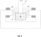
- Fig. 3 is a diagram illustrating a horizontal magnetic field being applied to crucible 10 containing melt 25 in a crystal growing apparatus.
- crucible 10 contains silicon melt 25 from which a crystal 27 is grown.
- the transition between the melt and the crystal is generally referred to as the crystal-melt interface (alternatively the melt-crystal, solid-melt or melt-solid interface) and is typically non-linear, for example concave, convex or gull-winged relative to the melt surface.
- Two magnetic poles 29 are placed in opposition to generate a magnetic field generally perpendicular to the crystal-growth direction and generally parallel to the melt surface 36.
- the magnetic poles 29 may be a conventional electromagnet, a superconductor electromagnet, or any other suitable magnet for producing a horizontal magnetic field of the desired strength.
- Application of a horizontal magnetic field gives rise to Lorentz force along axial direction, in a direction opposite of fluid motion, opposing forces driving melt convection.
- the convection in the melt is thus suppressed, and the axial temperature gradient in the crystal near the interface increases.
- the melt-crystal interface then moves upward to the crystal side to accommodate the increased axial temperature gradient in the crystal near the interface and the contribution from the melt convection in the crucible decreases.
- the horizontal configuration has the advantage of efficiency in damping a convective flow at the melt surface 36.
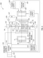
- Fig. 4 is a block diagram of a crystal growing system 100.
- System 100 employs a Czochralski crystal growth method to produce a semiconductor ingot.
- system 100 is configured to produce a cylindrical semiconductor ingot having an ingot diameter of one-hundred and fifty millimeters (150 mm), or greater than one-hundred fifty millimeters (150 mm), more specifically in a range from approximately 150 mm to 460 mm, and even more specifically, a diameter of approximately three-hundred millimeters (300 mm).
- system 100 is configured to produce a semiconductor ingot having a two-hundred millimeter (200 mm) ingot diameter or a four-hundred and fifty millimeter (450 mm) ingot diameter.
- system 100 is configured to produce a semiconductor ingot with a total ingot length of at least nine hundred millimeters (900 mm). In some cases, the system is configured to produce a semiconductor ingot with a length of one thousand nine hundred and fifty millimeters (1950 mm), two thousand two hundred and fifty millimeters (2250 mm), two thousand three hundred and fifty millimeters (2350 mm), or longer than 2350 mm.
- system 100 is configured to produce a semiconductor ingot with a total ingot length ranging from approximately nine hundred millimeters (900 mm) to twelve hundred millimeters (1200 mm), between approximately 900 mm and approximately two thousand millimeters (2000 mm), or between approximately 900 mm and approximately two thousand five hundred millimeters (2500 mm). In some cases, the system is configured to produce a semiconductor ingot with a total ingot length greater than 2000 mm.
- the crystal growing system 100 includes a vacuum chamber 101 enclosing crucible 10.
- a side heater 105 for example, a resistance heater, surrounds crucible 10.
- a bottom heater 106 for example, a resistance heater, is positioned below crucible 10.
- a crucible drive unit 107 e.g., a motor
- Crucible drive unit 107 may also raise and/or lower crucible 10 as desired during the growth process.
- silicon melt 25 having a melt level or melt surface 36.
- system 100 pulls a single crystal 27, starting with a seed crystal 115 attached to a pull shaft or cable 117, from melt 25.
- pull shaft or cable 117 is connected by way of a pulley (not shown) to a drum (not shown), or any other suitable type of lifting mechanism, for example, a shaft, and the other end is connected to a chuck (not shown) that holds seed crystal 115 and crystal 27 grown from seed crystal 115.
- Crucible 10 and single crystal 27 have a common axis of symmetry 38.
- Crucible drive unit 107 can raise crucible 10 along axis 38 as the melt 25 is depleted to maintain melt level 36 at a desired height.
- a crystal drive unit 121 similarly rotates pull shaft or cable 117 in a direction 110 opposite the direction in which crucible drive unit 107 rotates crucible 10 (e.g., counter-rotation). In cases using iso-rotation, crystal drive unit 121 may rotate pull shaft or cable 117 in the same direction in which crucible drive unit 107 rotates crucible 10 (e.g., in the clockwise direction). Iso-rotation may also be referred to as a co-rotation.
- crystal drive unit 121 raises and lowers crystal 27 relative to melt level 36 as desired during the growth process.
- a quantity of polycrystalline silicon, or polysilicon is charged to crucible 10.
- a heater power supply 123 energizes resistance heaters 105 and 106, and insulation 125 lines the inner wall of vacuum chamber 101.
- a gas supply 127 e.g., a bottle feeds argon gas to vacuum chamber 101 via a gas flow controller 129 as a vacuum pump 131 removes gas from vacuum chamber 101.
- An outer chamber 133 which is fed with cooling water from a reservoir 135, surrounds vacuum chamber 101.
- a temperature sensor such as a photocell 139 (or pyrometer) measures the temperature of melt 25 at its surface, and a diameter transducer 141 measures a diameter of single crystal 27.
- system 100 does not include an upper heater. The presence of an upper heater, or lack of an upper heater, alters cooling characteristics of crystal 27.
- Magnetic poles 29 are positioned outside the vacuum chamber 101 to produce a horizontal magnetic field (shown in Fig. 3 ). Although illustrated approximately centered on the melt surface 36, the position of the magnetic poles 29 relative to the melt surface 36 may be varied to adjust the position of the maximum gauss plane (MGP) relative to the melt surface 36.
- a reservoir 153 provides cooling water to the magnetic poles 29 before draining via cooling water return manifold 137.
- a ferrous shield 155 surrounds magnetic poles 29 to reduce stray magnetic fields and to enhance the strength of the field produced.
- a control unit 143 is used to regulate the plurality of process parameters including at least one of crystal rotation rate, crucible rotation rate, and magnetic field strength.
- the control unit 143 may include a memory 173 and processor 144 that processes the signals received from various sensors of the system 100 including photocell 139 and diameter transducer 141, as well as to control one or more devices of system 100 including: crucible drive unit 107, crystal drive unit 121, heater power supply 123, vacuum pump 131, gas flow controller 129 (e.g., an argon flow controller), magnetic poles power supply 149, and any combination thereof.
- the memory 173 may store instructions that, when executed by the processor 144 cause the processor to perform one or more of the methods described herein. That is, the instructions configure the control unit 143 to perform one or more methods, processes, or procedures described herein.
- Control unit 143 may be a computer system.
- Computer systems as described herein, refer to any known computing device and computer system. As described herein, all such computer systems include a processor and a memory. However, any processor in a computer system referred to herein may also refer to one or more processors wherein the processor may be in one computing device or a plurality of computing devices acting in parallel. Additionally, any memory in a computer device referred to herein may also refer to one or more memories wherein the memories may be in one computing device or a plurality of computing devices acting in parallel. Further, the computer system may located near the system 100 (e.g., in the same room, or in an adjacent room), or may be remotely located and coupled to the rest of the system via a network, such as an Ethernet or the Internet.
- a network such as an Ethernet or the Internet.
- processor refers to central processing units, microprocessors, microcontrollers, reduced instruction set circuits (RISC), application specific integrated circuits (ASIC), logic circuits, and any other circuit or processor capable of executing the functions described herein.
- the above are examples only, and are thus not intended to limit in any way the definition and/or meaning of the term "processor.”
- the memory may include random access memory (RAM) such as dynamic RAM (DRAM) or static RAM (SRAM), read-only memory (ROM), erasable programmable read-only memory (EPROM), electrically erasable programmable read-only memory (EEPROM), and non-volatile RAM (NVRAM).
- RAM random access memory
- DRAM dynamic RAM
- SRAM static RAM
- ROM read-only memory
- EPROM erasable programmable read-only memory
- EEPROM electrically erasable programmable read-only memory
- NVRAM non-volatile RAM
- a computer program is provided to enable control unit 143, and this program is embodied on a computer readable medium.
- the computer readable medium may include the memory 173 of the control unit 143.
- the computer system is executed on a single computer system.
- the computer system may comprise multiple computer systems, connection to a server computer, or a cloud computing environment.
- the computer system includes multiple components distributed among a plurality of computing devices.
- One or more components may be in the form of computer-executable instructions embodied in a computer-readable medium.
- the computer system may be configured to receive measurements from one or more sensors including: temperature sensor 139, diameter transducer 141, and any combination thereof, as well as to control one or more devices of system 100 including: crucible drive unit 107, crystal drive unit 121, heater power supply 123, vacuum pump 131, gas flow controller 129 (e.g., an argon flow controller), magnetic poles power supply 149, and any combination thereof as described herein and illustrated in Fig. 4 .
- the computer system performs all of the steps used to control one or more devices of system 100 as described herein.
- the loss of zero dislocation (ZD) structure (quantified by LZD rate) is generally higher during silicon crystal Cz growth in a horizontal magnet (HMCZ) field versus growth in a Cusp (or vertical) magnetic field.
- HMCZ horizontal magnet
- Cusp or vertical
- the LZD rate in HMCZ can be lowered dramatically if the crystal is grown in a synthetic lined crucible versus a natural sand lined crucible.
- the cost of synthetic lined crucibles is higher than natural sand.
- the thin (roughly 2mm thickness) synthetic liner dissolves in a relatively short process time, leaving the backing sand layer exposed to the melt, which allows quartz particles to enter the melt and hit the growing crystal.
- the exposure of bubbles in the liner or even from the backing sand into the melt is higher.
- the process hot hours are generally limited to less than ⁇ 250 hours, which is much shorter process time than achievable for natural sand crucibles (approximately 400-500 hours or more). Because the hot time for crystal growth depends on the process conditions, HZ configuration, and attempts, recharge capability and multiple rod growth per batch can be impacted using synthetic lined crucibles. Therefore, silicon growth using HMCZ in synthetic lined crucibles generally requires optimization of the crucible condition to ensure the best ZD rate and lowest attempts so that maximum recharge capability can be achieved.
- a horizontal magnet in Cz growth enhances the melt flow with an irregular velocity melt wave continuously knocking against the crucible wall surface with a strong force in a transient behavior.
- the crucible surface condition is very critical for quartz piece generation which directly relates to the ZD success.
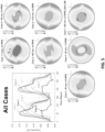
- Fig. 5 in which the melt flow and temperature field of the melt are significantly impacted by the magnetic field strength and MGP position. As shown in the figure, the temperature variation of the circumferential direction at the melt surface is markedly changed by the magnetic field direction.
- a cristobalite layer is formed on the wettable surface of the interior of the crucible.
- the wettable surface generally refers to the surface of the crucible that may be in contact with the melt during silicon production.
- the wettable surface generally includes the interior bottom of the crucible, at least a portion of the interior sidewalls of the crucible, and the interior portions connecting the interior sidewalls and bottom of the crucible.
- the wettable surface is all of the interior surface of the crucible 10 below and including the melt surface 36.
- the wettable surface may also extend above the melt surface 36.
- the second technique described in this invention is to increase the rotational speed of the crucible.
- LZDs may also be reduced by enabling the formation of a generally uniform crystalline SiO 2 layer (referred to as cristobalite layer) on the crucible's wettable surface.
- This layer is more stable and stronger than amorphous quartz itself, and thereby it is more resistant to melt attack by stress or mechanical impact.
- the cristobalite layer reduces quartz particle generation.
- the first method is to use pre-coated crucibles precoated with a compound, such as BaOH, that will promote cristobalite growth, and the other is to add a suitable melt modifier (MM) into the melt before crystal growth.
- suitable MMs include barium (Ba) and strontium (Sr). More specifically, examples of suitable MMs include barium carbonate (BaCO 3 ), barium oxide (BaO), and strontium carbonate (SrCO 3 ).
- Cristobalite formation on the amorphous quartz inner wall is governed by pressure, Oi concentration, H 2 O and hydrogen content, and temperature.
- the formation and growth of a crystalline layer on the crucible wall is governed by the temperature of the crucible wall and concentration of the MM, which is consumed by the crucible.
- Fig. 6 compares the crystallization rate as a function of time for no MM and an 8% AL 2 O 3 MM.
- Fig. 7 compares the thickness of the layer formed as a function of time at a temperature of 1360°C for no MM, an 8% AL 2 O 3 MM, and a barium based MM.
- the formation and growth of a uniform cristobalite layer either through pre-coating on the crucible or post addition of melt modifier into the melt is started during stabilization mode prior to crystal growth (i.e. after melting of polysilicon or during the melting).
- the MM is introduced after meltdown, so the formation speed of the cristobalite is slower than in an otherwise pre-coated case.
- post addition of the MM can yield lower air pocket (APK) losses because bubbles formed and trapped at the crucible wall can be released to the surface prior to the formation of the stable cristobalite layer.
- the cristobalite thickness is estimated to be greater than 2mm with an appropriate amount of MM added to increase the formation rate of the cristobalite.
- a cristobalite layer of less than 1.0mm is typically formed on the surface of the crucible (whether natural sand or synthetic).
- the cristobalite layer has a thickness of greater than 0.25 mm.
- Other embodiments include a cristobalite layer of approximately 2.0mm, greater than 1.5 mm, greater than 1.0mm, greater than 0.75mm, or greater than 0.5mm formed on the wettable surface of the crucible.
- the cristobalite layer is less than 3.0mm thick, less than 2.0mm thick, less than 1.25 mm thick, or less than 1.0mm thick.
- the cristobalite layer falls within a range defined by the minima and maxima above, such as between 0.25mm and 1.25mm. Generally, too thin a cristobalite layer may be insufficient to provide the benefits described herein, while too thick a cristobalite layer may be more likely to break and enter the melt (potentially contributing to an LZD) during silicon production.
- melt modifier addition described above forms a uniform crystalline layer at the crucible wettable surface and this crystalline structure has a strong resistance against the thermomechanical stress induced by the irregular (transient) melt flow produced during HMCZ.
- the formation of a thick and uniform cristobalite can resist the stress and impact from the melt flow, reducing crucible surface damage (i.e., resisting damage generating quartz particles in the melt) which will increase the ZD success.
- CR is the crucible rotation in RPM
- a Success %_3 of 0.0 is a ZD fail (LZD)
- a Success %_3 of 1.0 is 100% ZD success.
- the sign of the crucible rotation indicates direction of rotation of the crucible. For some pulls, the crucible rotation ramped between speeds during portions of the pull, an arbitrary value of crucible rotation was selected for plotting, and the data was collected from greater than 1000mm body length to approximately OE of the crystal. Results clearly show that higher ZD success ratio is achieved with increasing the absolute value of the speed of crucible rotation and quantity of melt modifier (in this case, Ba based).
- some embodiments of the present invention use a MM more than 1.7 grams per square meter of the wettable surface area of crucible during an HMCZ process at any C/R rate to improve the ZD success rate.
- a MM between 1.7 and 2.0 grams/m 2 of the wettable surface of the crucible is used.
- a MM between 1.7 and 5.4 grams/m 2 of the wettable surface of the crucible is used.
- a MM greater than 5.4 grams/m 2 of the wettable surface of the crucible may be used, but the large amount of MM might cause LZD in multiple recharge processes.
- the quantities above e.g., 1.7 grams/m 2
- Similar embodiments using BaO or SrCO 3 include an amount of the particular MM functionally equivalent to the amount of BaCO 3 .
- Some embodiments use a MM between 0 and 0.5g/m 2 .
- the crucible rotation in the method of the invention is greater than 2.0 RPM.
- the crucible is a natural sand crucible.
- Embodiments of the methods described herein achieve superior results compared to prior methods.
- the methods described herein facilitate producing silicon with a higher ZD success rate than some other methods.
Landscapes
- Chemical & Material Sciences (AREA)
- Engineering & Computer Science (AREA)
- Crystallography & Structural Chemistry (AREA)
- Materials Engineering (AREA)
- Metallurgy (AREA)
- Organic Chemistry (AREA)
- Crystals, And After-Treatments Of Crystals (AREA)
Description
- This invention generally relates to the production of silicon ingots, and more specifically, to methods for achieving a high success ratio producing silicon ingots in the Czochralski process using a horizontal magnetic field.
- During the 1990's, at least some high quality silicon growth was mainly controlled by the thermal condition of the puller and more specifically the hot zone (HZ) design itself, because the ratio of the pulling speed to the thermal gradient (v/G) was considered the dominant factor. In the late 1990's, further consideration of the crystal/melt interface at the same v/G was included in the growth of at least some high quality silicon. At that time, application of high quality silicon to memory devices really expanded as more customers transitioned from epi to polished and from 200mm to 300mm silicon. Soon after, it became established that high quality silicon growth requires very stable process growth conditions and controlled melt flow to achieve the specific crystal/melt needed to achieve the desired low crystal defectivity during growth.
- Peripherally, as silicon crystal growth transitioned from 200mm to 300mm and corresponding charge sizes increased to maintain productivity, the need for magnetic field application to stabilize melt flow in the increasing melt volume was recognized as a dominate feature.
- Several silicon manufactures transitioned to a horizontal magnetic field Czochralski process (HMCZ) in the early 2000's when high quality 300mm silicon production started in order to control the crystal/melt interface effectively. Other silicon manufactures used a cusp magnetic field for 300mm production of high quality silicon. In both cases, magnetic field in the silicon melt had a dramatic impact on crystal quality and performance and every manufacturer developed their own technique to optimize performance and quality from the onset.
- During the process of producing single crystal silicon ingots with the CZ process and a magnetic field, oxygen may be introduced into silicon crystal ingots through a melt-solid or melt crystal interface. The oxygen may cause various defects in wafers produced from the ingots, reducing the yield of semiconductor devices fabricated using the ingots. For example, memory devices, insulated-gate bipolar transistors (IGBTs), high quality radio-frequency (RF), high resistivity silicon on insulator (HR-SOI), and charge trap layer SOI (CTL-SOI) applications typically require a low interstitial oxygen concentration (Oi) in order to achieve high resistivity. In the case of HMCZ process, it was believed that the process typically requires a very low crucible rotation (C/R) to control oxygen in the growing crystal, particularly to control oxygen inclusion to the desired range applicable for memory devices. Further, a higher occurrence ratio of lost zero dislocation (LZD) from the crown to the end of body was found in HMCZ as compared to processes using a cusp magnetic field.
- Thus, there exists a need for methods that reduce LZD losses with HMCZ growth and provide an improved ZD success ratio for high quality silicon growth from crown to body.
-
JP 2010 030867 A US 2014/174339 A1 describes a method for manufacturing a silicon single crystal wherein, after the raw material melting step and before the pulling step, there are performed: a cristobalitizing step while applying a magnetic field; and a dissolving step of partially dissolving the cristobalite.JP 2018 138508 A - This background section is intended to introduce the reader to various aspects of art that may be related to various aspects of the present invention, which are described and/or claimed below. This discussion is believed to be helpful in providing the reader with background information to facilitate a better understanding of the various aspects of the present invention. Accordingly, it should be understood that these statements are to be read in this light, and not as admissions of prior art.
- In one aspect of this invention, a method for producing a silicon ingot by the horizontal magnetic field Czochralski method includes rotating a natural sand crucible containing a silicon melt at more than two revolutions per minute, applying a horizontal magnetic field to the crucible, contacting the silicon melt with a seed crystal, and withdrawing the seed crystal from the silicon melt while rotating the crucible at more than two revolutions per minute to form a silicon ingot. The crucible has a wettable surface with a cristobalite layer formed thereon, the cristobalite layer having a thickness of greater than 0.25 mm.
-
-
Fig. 1 is a top view of a crucible. -
Fig. 2 is a side view of the crucible shown inFig. 1 . -
Fig. 3 is a schematic illustrating a horizontal magnetic field applied to a crucible containing a melt in a crystal growing apparatus. -
Fig. 4 is a block diagram of a crystal growing system. -
Fig. 5 presents temperature field in melt free surface by MGP in mm and crucible rotation in RPM. -
Fig. 6 is a graph of crystallization rate as a function of time. -
Fig. 7 is a graph of the thickness of the layer formed as a function of time at a temperature of 1360°C. -
Fig. 8 is a contour plot of ZD success ratio by crucible rotation and the quantity of melt modifier in a natural sand crucible. - Like reference symbols in the various drawings indicate like elements.
- Referring initially to
Figs. 1 and 2 , a crucible is indicated generally at 10. A cylindrical coordinate system forcrucible 10 includes aradial direction R 12, anangular direction θ 14, and anaxial direction Z 16. Thecrucible 10 contains amelt 25 having amelt surface 36. Acrystal 27 is grown from themelt 25. Themelt 25 may contain one or moreconvective flow cells crucible 10 and rotation of thecrucible 10 and/orcrystal 27 in theangular direction θ 14. The structure and interaction of these one or moreconvective flow cells -
Fig. 3 is a diagram illustrating a horizontal magnetic field being applied tocrucible 10 containingmelt 25 in a crystal growing apparatus. As shown,crucible 10 containssilicon melt 25 from which acrystal 27 is grown. The transition between the melt and the crystal is generally referred to as the crystal-melt interface (alternatively the melt-crystal, solid-melt or melt-solid interface) and is typically non-linear, for example concave, convex or gull-winged relative to the melt surface. Twomagnetic poles 29 are placed in opposition to generate a magnetic field generally perpendicular to the crystal-growth direction and generally parallel to themelt surface 36. Themagnetic poles 29 may be a conventional electromagnet, a superconductor electromagnet, or any other suitable magnet for producing a horizontal magnetic field of the desired strength. Application of a horizontal magnetic field gives rise to Lorentz force along axial direction, in a direction opposite of fluid motion, opposing forces driving melt convection. The convection in the melt is thus suppressed, and the axial temperature gradient in the crystal near the interface increases. The melt-crystal interface then moves upward to the crystal side to accommodate the increased axial temperature gradient in the crystal near the interface and the contribution from the melt convection in the crucible decreases. The horizontal configuration has the advantage of efficiency in damping a convective flow at themelt surface 36. -
Fig. 4 is a block diagram of acrystal growing system 100.System 100 employs a Czochralski crystal growth method to produce a semiconductor ingot. In this case,system 100 is configured to produce a cylindrical semiconductor ingot having an ingot diameter of one-hundred and fifty millimeters (150 mm), or greater than one-hundred fifty millimeters (150 mm), more specifically in a range from approximately 150 mm to 460 mm, and even more specifically, a diameter of approximately three-hundred millimeters (300 mm). In other cases,system 100 is configured to produce a semiconductor ingot having a two-hundred millimeter (200 mm) ingot diameter or a four-hundred and fifty millimeter (450 mm) ingot diameter. In addition, in one case,system 100 is configured to produce a semiconductor ingot with a total ingot length of at least nine hundred millimeters (900 mm). In some cases, the system is configured to produce a semiconductor ingot with a length of one thousand nine hundred and fifty millimeters (1950 mm), two thousand two hundred and fifty millimeters (2250 mm), two thousand three hundred and fifty millimeters (2350 mm), or longer than 2350 mm. In other cases,system 100 is configured to produce a semiconductor ingot with a total ingot length ranging from approximately nine hundred millimeters (900 mm) to twelve hundred millimeters (1200 mm), between approximately 900 mm and approximately two thousand millimeters (2000 mm), or between approximately 900 mm and approximately two thousand five hundred millimeters (2500 mm). In some cases, the system is configured to produce a semiconductor ingot with a total ingot length greater than 2000 mm. - The
crystal growing system 100 includes avacuum chamber 101 enclosingcrucible 10. Aside heater 105, for example, a resistance heater, surroundscrucible 10. A bottom heater 106, for example, a resistance heater, is positioned belowcrucible 10. During heating and crystal pulling, a crucible drive unit 107 (e.g., a motor) rotatescrucible 10, for example, in the clockwise direction as indicated by thearrow 108.Crucible drive unit 107 may also raise and/or lowercrucible 10 as desired during the growth process. Withincrucible 10 issilicon melt 25 having a melt level or meltsurface 36. In operation,system 100 pulls asingle crystal 27, starting with aseed crystal 115 attached to a pull shaft or cable 117, frommelt 25. One end of pull shaft or cable 117 is connected by way of a pulley (not shown) to a drum (not shown), or any other suitable type of lifting mechanism, for example, a shaft, and the other end is connected to a chuck (not shown) that holdsseed crystal 115 andcrystal 27 grown fromseed crystal 115. -
Crucible 10 andsingle crystal 27 have a common axis ofsymmetry 38.Crucible drive unit 107 can raisecrucible 10 alongaxis 38 as themelt 25 is depleted to maintainmelt level 36 at a desired height. Acrystal drive unit 121 similarly rotates pull shaft or cable 117 in adirection 110 opposite the direction in whichcrucible drive unit 107 rotates crucible 10 (e.g., counter-rotation). In cases using iso-rotation,crystal drive unit 121 may rotate pull shaft or cable 117 in the same direction in whichcrucible drive unit 107 rotates crucible 10 (e.g., in the clockwise direction). Iso-rotation may also be referred to as a co-rotation. In addition,crystal drive unit 121 raises and lowerscrystal 27 relative to meltlevel 36 as desired during the growth process. - According to the Czochralski single crystal growth process, a quantity of polycrystalline silicon, or polysilicon, is charged to
crucible 10. Aheater power supply 123 energizesresistance heaters 105 and 106, andinsulation 125 lines the inner wall ofvacuum chamber 101. A gas supply 127 (e.g., a bottle) feeds argon gas to vacuumchamber 101 via agas flow controller 129 as avacuum pump 131 removes gas fromvacuum chamber 101. Anouter chamber 133, which is fed with cooling water from areservoir 135, surroundsvacuum chamber 101. - The cooling water is then drained to a cooling
water return manifold 137. Typically, a temperature sensor such as a photocell 139 (or pyrometer) measures the temperature ofmelt 25 at its surface, and adiameter transducer 141 measures a diameter ofsingle crystal 27. In this configuration,system 100 does not include an upper heater. The presence of an upper heater, or lack of an upper heater, alters cooling characteristics ofcrystal 27. -
Magnetic poles 29 are positioned outside thevacuum chamber 101 to produce a horizontal magnetic field (shown inFig. 3 ). Although illustrated approximately centered on themelt surface 36, the position of themagnetic poles 29 relative to themelt surface 36 may be varied to adjust the position of the maximum gauss plane (MGP) relative to themelt surface 36. Areservoir 153 provides cooling water to themagnetic poles 29 before draining via coolingwater return manifold 137. A ferrous shield 155 surroundsmagnetic poles 29 to reduce stray magnetic fields and to enhance the strength of the field produced. - A
control unit 143 is used to regulate the plurality of process parameters including at least one of crystal rotation rate, crucible rotation rate, and magnetic field strength. In various cases, thecontrol unit 143 may include a memory 173 andprocessor 144 that processes the signals received from various sensors of thesystem 100 including photocell 139 anddiameter transducer 141, as well as to control one or more devices ofsystem 100 including:crucible drive unit 107,crystal drive unit 121,heater power supply 123,vacuum pump 131, gas flow controller 129 (e.g., an argon flow controller), magneticpoles power supply 149, and any combination thereof. The memory 173 may store instructions that, when executed by theprocessor 144 cause the processor to perform one or more of the methods described herein. That is, the instructions configure thecontrol unit 143 to perform one or more methods, processes, or procedures described herein. -
Control unit 143 may be a computer system. Computer systems, as described herein, refer to any known computing device and computer system. As described herein, all such computer systems include a processor and a memory. However, any processor in a computer system referred to herein may also refer to one or more processors wherein the processor may be in one computing device or a plurality of computing devices acting in parallel. Additionally, any memory in a computer device referred to herein may also refer to one or more memories wherein the memories may be in one computing device or a plurality of computing devices acting in parallel. Further, the computer system may located near the system 100 (e.g., in the same room, or in an adjacent room), or may be remotely located and coupled to the rest of the system via a network, such as an Ethernet or the Internet. - The term processor, as used herein, refers to central processing units, microprocessors, microcontrollers, reduced instruction set circuits (RISC), application specific integrated circuits (ASIC), logic circuits, and any other circuit or processor capable of executing the functions described herein. The above are examples only, and are thus not intended to limit in any way the definition and/or meaning of the term "processor." The memory may include random access memory (RAM) such as dynamic RAM (DRAM) or static RAM (SRAM), read-only memory (ROM), erasable programmable read-only memory (EPROM), electrically erasable programmable read-only memory (EEPROM), and non-volatile RAM (NVRAM).
- In one case, a computer program is provided to enable
control unit 143, and this program is embodied on a computer readable medium. The computer readable medium may include the memory 173 of thecontrol unit 143. In an example, the computer system is executed on a single computer system. Alternatively, the computer system may comprise multiple computer systems, connection to a server computer, or a cloud computing environment. In some cases, the computer system includes multiple components distributed among a plurality of computing devices. One or more components may be in the form of computer-executable instructions embodied in a computer-readable medium. - In one case, the computer system may be configured to receive measurements from one or more sensors including: temperature sensor 139,
diameter transducer 141, and any combination thereof, as well as to control one or more devices ofsystem 100 including:crucible drive unit 107,crystal drive unit 121,heater power supply 123,vacuum pump 131, gas flow controller 129 (e.g., an argon flow controller), magneticpoles power supply 149, and any combination thereof as described herein and illustrated inFig. 4 . The computer system performs all of the steps used to control one or more devices ofsystem 100 as described herein. - The loss of zero dislocation (ZD) structure (quantified by LZD rate) is generally higher during silicon crystal Cz growth in a horizontal magnet (HMCZ) field versus growth in a Cusp (or vertical) magnetic field. However, the LZD rate in HMCZ can be lowered dramatically if the crystal is grown in a synthetic lined crucible versus a natural sand lined crucible. But while the ZD rate is better, the cost of synthetic lined crucibles is higher than natural sand. Additionally, the thin (roughly 2mm thickness) synthetic liner dissolves in a relatively short process time, leaving the backing sand layer exposed to the melt, which allows quartz particles to enter the melt and hit the growing crystal. Thus, the exposure of bubbles in the liner or even from the backing sand into the melt is higher. To avoid bubble exposure and/or backing sand contamination by dissolution when using synthetic lined crucibles, the process hot hours are generally limited to less than ~250 hours, which is much shorter process time than achievable for natural sand crucibles (approximately 400-500 hours or more). Because the hot time for crystal growth depends on the process conditions, HZ configuration, and attempts, recharge capability and multiple rod growth per batch can be impacted using synthetic lined crucibles. Therefore, silicon growth using HMCZ in synthetic lined crucibles generally requires optimization of the crucible condition to ensure the best ZD rate and lowest attempts so that maximum recharge capability can be achieved.
- Further, a horizontal magnet in Cz growth enhances the melt flow with an irregular velocity melt wave continuously knocking against the crucible wall surface with a strong force in a transient behavior. In this case, the crucible surface condition is very critical for quartz piece generation which directly relates to the ZD success. This is illustrated in
Fig. 5 , in which the melt flow and temperature field of the melt are significantly impacted by the magnetic field strength and MGP position. As shown in the figure, the temperature variation of the circumferential direction at the melt surface is markedly changed by the magnetic field direction. - These and other difficulties may be overcome or mitigated in embodiments of the present invention through use of both of two techniques described in detail below. Generally, in the first technique, a cristobalite layer is formed on the wettable surface of the interior of the crucible. The wettable surface generally refers to the surface of the crucible that may be in contact with the melt during silicon production. The wettable surface generally includes the interior bottom of the crucible, at least a portion of the interior sidewalls of the crucible, and the interior portions connecting the interior sidewalls and bottom of the crucible. In
Fig. 2 , the wettable surface is all of the interior surface of thecrucible 10 below and including themelt surface 36. The wettable surface may also extend above themelt surface 36. The second technique described in this invention is to increase the rotational speed of the crucible. - In general, a strong and unsteady melt flow is induced by an HMCZ magnetic field and this can generate strong thermo-mechanical stress and mechanical impact on the crucible wall causing quartz particle generation. However, high crucible rotation (C/R) will produce faster convective flow near the crucible wall surface, which can interfere with the melt flow driven by a magnetic field. This will reduce the stress and impact on the wall surface. Consequently, the generation of quartz particles at the wall surface is reduced which in turn reduces LZDs during crystal growth.
- LZDs may also be reduced by enabling the formation of a generally uniform crystalline SiO2 layer (referred to as cristobalite layer) on the crucible's wettable surface. This layer is more stable and stronger than amorphous quartz itself, and thereby it is more resistant to melt attack by stress or mechanical impact. Thus, the cristobalite layer reduces quartz particle generation.
- There are at least two methods to promote crystalline layer growth on quartz crucibles. The first method is to use pre-coated crucibles precoated with a compound, such as BaOH, that will promote cristobalite growth, and the other is to add a suitable melt modifier (MM) into the melt before crystal growth. Examples of suitable MMs include barium (Ba) and strontium (Sr). More specifically, examples of suitable MMs include barium carbonate (BaCO3), barium oxide (BaO), and strontium carbonate (SrCO3).
- Cristobalite formation on the amorphous quartz inner wall is governed by pressure, Oi concentration, H2O and hydrogen content, and temperature. As shown in
Figs. 6 and 7 , the formation and growth of a crystalline layer on the crucible wall is governed by the temperature of the crucible wall and concentration of the MM, which is consumed by the crucible.Fig. 6 compares the crystallization rate as a function of time for no MM and an 8% AL2O3 MM.Fig. 7 compares the thickness of the layer formed as a function of time at a temperature of 1360°C for no MM, an 8% AL2O3 MM, and a barium based MM. These charts indicates that a proper MM addition (e.g., a barium based MM) into the melt or a pre-coating of a barium compound generates an uniform and thick crystalline (i.e., cristobalite) layer on the wall of natural sand crucibles giving similar behavior and performance to synthetic lined crucibles. Because the cristobalite layer has slower dissolution rate than the fused quartz, the generation of quartz pieces by thermo or mechanical stress is decreased so the crystal LZD occurrence is decreased thereafter. Further, the generation of secondary bubbles in the Bubble Free Layer (BFL) of the natural sand crucible and its propagation into the melt is much less than that of synthetic lined crucible in general due to the difference of material properties. - The formation and growth of a uniform cristobalite layer either through pre-coating on the crucible or post addition of melt modifier into the melt is started during stabilization mode prior to crystal growth (i.e. after melting of polysilicon or during the melting). In case of a post MM addition, the MM is introduced after meltdown, so the formation speed of the cristobalite is slower than in an otherwise pre-coated case. However, post addition of the MM can yield lower air pocket (APK) losses because bubbles formed and trapped at the crucible wall can be released to the surface prior to the formation of the stable cristobalite layer. Because it typically takes 3 to 7 hours from the start of the stabilization step to the start of body growth, the cristobalite thickness is estimated to be greater than 2mm with an appropriate amount of MM added to increase the formation rate of the cristobalite. In practice, a cristobalite layer of less than 1.0mm is typically formed on the surface of the crucible (whether natural sand or synthetic). Some special cases, such as a heavily doped process for P++ or N++, yield a thicker cristobalite layer by adding a large amount of MM. In such cases a cristobalite layer of approximately 1.0mm (+/-) is formed. These thicknesses differ from the 2.0mm because although the cristobalite layer is grown by hot time as shown in
Fig 7 , wet cristobalite layer is continuously being dissolved to melt. In the present invention, the cristobalite layer has a thickness of greater than 0.25 mm. Other embodiments include a cristobalite layer of approximately 2.0mm, greater than 1.5 mm, greater than 1.0mm, greater than 0.75mm, or greater than 0.5mm formed on the wettable surface of the crucible. In some embodiments the cristobalite layer is less than 3.0mm thick, less than 2.0mm thick, less than 1.25 mm thick, or less than 1.0mm thick. In some embodiments, the cristobalite layer falls within a range defined by the minima and maxima above, such as between 0.25mm and 1.25mm. Generally, too thin a cristobalite layer may be insufficient to provide the benefits described herein, while too thick a cristobalite layer may be more likely to break and enter the melt (potentially contributing to an LZD) during silicon production. - Melt modifier addition described above forms a uniform crystalline layer at the crucible wettable surface and this crystalline structure has a strong resistance against the thermomechanical stress induced by the irregular (transient) melt flow produced during HMCZ. The formation of a thick and uniform cristobalite can resist the stress and impact from the melt flow, reducing crucible surface damage (i.e., resisting damage generating quartz particles in the melt) which will increase the ZD success.
- As mentioned previously, a strong convective flow caused by higher crucible rotation will reduce the variation of temperature in the melt free surface and reduce the melt flow induced by a horizontal magnet as seen in
Case 6 inFig. 5 . Incase 6, C/R is 1.6 RPM as compared to 0.6 RPM in cases 1-5 and 7. In other words, the force produced by the magnetic field from the melt to the crucible wall surface is reduced or blocked by the convective flow related with higher crucible rotation. Thereby, the possibility of quartz piece generation due to damage of crucible wall surface is decreased, also improving the potential of ZD success. - A test condition was performed to understand ZD success and on both synthetic lined and natural sand crucibles in a horizontal magnet as a function of crucible rotation speed and the quantity of melt modifier addition. The synthetic crucible showed high ZD success ratio across a broad range of crucible rotation and MM. For the natural sand lined crucible, a total of 96 trials with 19 different conditions were completed and the results are summarized with a contour plot in
Fig. 8 . The data forFig. 8 was from approximately 200mm body length to approximately OE of the crystal. InFig. 8 , CR is the crucible rotation in RPM, a Success %_3 of 0.0 is a ZD fail (LZD), and a Success %_3 of 1.0 is 100% ZD success. The sign of the crucible rotation indicates direction of rotation of the crucible. For some pulls, the crucible rotation ramped between speeds during portions of the pull, an arbitrary value of crucible rotation was selected for plotting, and the data was collected from greater than 1000mm body length to approximately OE of the crystal. Results clearly show that higher ZD success ratio is achieved with increasing the absolute value of the speed of crucible rotation and quantity of melt modifier (in this case, Ba based). - The use of increased speed of crucible rotation and the creation of a cristobalite layer are shown to individually and in combination result in improved ZD outcomes. At lower C/R, such as between 0 and 2 RPM, addition of suitable MM (or use of precoated crucible) is needed to increase the ZD success ratio. As the C/R is increased to between 2 RPM and 5 RPM, the amount of MM needed to gain an equivalent success rate decreases and may even be zero MM. Within this range, additional gains in ZD success ratio may be obtained through use of at least some MM. When the C/R exceeds 5 RPM there is generally no ZD concern from the crucible and no MM is likely to be needed. However, at such speeds, additional process condition will likely be required to control the quality of the products, because it may have other issues such as oxygen control due to melt flow velocity and melt level control caused by centrifugal force.
- Thus, some embodiments of the present invention use a MM more than 1.7 grams per square meter of the wettable surface area of crucible during an HMCZ process at any C/R rate to improve the ZD success rate. In some embodiments, a MM between 1.7 and 2.0 grams/m2 of the wettable surface of the crucible is used. In still other embodiments, a MM between 1.7 and 5.4 grams/m2 of the wettable surface of the crucible is used. In still other embodiments, a MM greater than 5.4 grams/m2 of the wettable surface of the crucible may be used, but the large amount of MM might cause LZD in multiple recharge processes. The quantities above (e.g., 1.7 grams/m2) are based on BaCO3 as the MM. Similar embodiments using BaO or SrCO3 include an amount of the particular MM functionally equivalent to the amount of BaCO3.
- Some embodiments use a MM between 0 and 0.5g/m2. The crucible rotation in the method of the invention is greater than 2.0 RPM. The crucible is a natural sand crucible.
- Embodiments of the methods described herein achieve superior results compared to prior methods. For example, the methods described herein facilitate producing silicon with a higher ZD success rate than some other methods.
Claims (11)
- A method for producing a silicon ingot by the horizontal magnetic field Czochralski method, the method comprising:rotating a natural sand crucible containing a silicon melt at more than two revolutions per minute, the crucible having a wettable surface with a cristobalite layer formed thereon, the cristobalite layer having a thickness of greater than 0.25 mm;applying a horizontal magnetic field to the crucible;contacting the silicon melt with a seed crystal; andwithdrawing the seed crystal from the silicon melt while rotating the crucible at more than two revolutions per minute to form a silicon ingot.
- The method of claim 1, wherein the method further comprises:adding solid-phase polycrystalline silicon to the natural sand crucible; andheating the polycrystalline silicon to form the silicon melt.
- The method of claim 2, further comprising adding a melt modifier to the natural sand crucible to form the cristobalite layer on the wettable surface of the natural sand crucible.
- The method of claim 3, wherein adding a melt modifier comprises adding the melt modifier while heating the polycrystalline silicon to form the silicon melt.
- The method of claim 3, wherein adding a melt modifier comprises adding the melt modifier after the silicon melt has been formed.
- The method of any of claims 3 to 5, wherein adding a melt modifier comprises adding barium carbonate (BaCO3).
- The method of claim 6, wherein adding barium carbonate comprises adding more than 1.7 grams per square meter of the wettable surface of the natural sand crucible.
- The method of any of claims 3 to 5, wherein adding a melt modifier comprises adding one of barium oxide (BaO) or strontium carbonate (SrCO3).
- The method of claim 8, wherein adding one of barium oxide or strontium carbonate comprises adding one of barium oxide or strontium carbonate in an amount substantially equivalent to 1.7 grams of barium carbonate per square meter of the wettable surface of the natural sand crucible.
- The method of claim 2, wherein adding solid-phase polycrystalline silicon to the natural sand crucible comprises adding solid-phase polycrystalline silicon to a natural sand crucible having a barium based coating already formed on the wettable surface of the natural sand crucible.
- The method of any preceding claim, wherein the cristobalite layer is greater than about 2.00 mm thick.
Priority Applications (1)
| Application Number | Priority Date | Filing Date | Title |
|---|---|---|---|
| EP24165596.8A EP4386117B1 (en) | 2019-12-13 | 2020-12-10 | Systems for production of silicon using a horizontal magnetic field |
Applications Claiming Priority (2)
| Application Number | Priority Date | Filing Date | Title |
|---|---|---|---|
| US201962947785P | 2019-12-13 | 2019-12-13 | |
| PCT/US2020/064231 WO2021119267A1 (en) | 2019-12-13 | 2020-12-10 | Systems and methods for production of silicon using a horizontal magnetic field |
Related Child Applications (2)
| Application Number | Title | Priority Date | Filing Date |
|---|---|---|---|
| EP24165596.8A Division EP4386117B1 (en) | 2019-12-13 | 2020-12-10 | Systems for production of silicon using a horizontal magnetic field |
| EP24165596.8A Division-Into EP4386117B1 (en) | 2019-12-13 | 2020-12-10 | Systems for production of silicon using a horizontal magnetic field |
Publications (2)
| Publication Number | Publication Date |
|---|---|
| EP4073295A1 EP4073295A1 (en) | 2022-10-19 |
| EP4073295B1 true EP4073295B1 (en) | 2024-05-01 |
Family
ID=74141884
Family Applications (2)
| Application Number | Title | Priority Date | Filing Date |
|---|---|---|---|
| EP24165596.8A Active EP4386117B1 (en) | 2019-12-13 | 2020-12-10 | Systems for production of silicon using a horizontal magnetic field |
| EP20838749.8A Active EP4073295B1 (en) | 2019-12-13 | 2020-12-10 | Methods for production of silicon using a horizontal magnetic field |
Family Applications Before (1)
| Application Number | Title | Priority Date | Filing Date |
|---|---|---|---|
| EP24165596.8A Active EP4386117B1 (en) | 2019-12-13 | 2020-12-10 | Systems for production of silicon using a horizontal magnetic field |
Country Status (7)
| Country | Link |
|---|---|
| US (2) | US11873574B2 (en) |
| EP (2) | EP4386117B1 (en) |
| JP (2) | JP7720843B2 (en) |
| KR (1) | KR102920295B1 (en) |
| CN (2) | CN114787429B (en) |
| TW (1) | TWI865685B (en) |
| WO (1) | WO2021119267A1 (en) |
Families Citing this family (5)
| Publication number | Priority date | Publication date | Assignee | Title |
|---|---|---|---|---|
| US20240035198A1 (en) * | 2022-07-29 | 2024-02-01 | Globalwafers Co., Ltd. | Systems and methods for forming single crystal silicon ingots with crucibles having a synthetic liner |
| US12486593B2 (en) | 2022-08-29 | 2025-12-02 | Globalwafers Co., Ltd. | Axial positioning of magnetic poles while producing a silicon ingot |
| US12486594B2 (en) | 2022-08-29 | 2025-12-02 | Globalwafers Co., Ltd. | Ingot puller apparatus that axially position magnetic poles |
| CN116005249B (en) * | 2022-12-26 | 2025-06-20 | 西安奕斯伟材料科技股份有限公司 | Single crystal silicon rod growth method and device |
| CN116749069A (en) * | 2023-06-13 | 2023-09-15 | 苏州鑫荣健身器材有限公司 | A massage chair movement gear polishing device |
Family Cites Families (24)
| Publication number | Priority date | Publication date | Assignee | Title |
|---|---|---|---|---|
| US5096857A (en) | 1990-10-22 | 1992-03-17 | E. I. Du Pont De Nemours And Company | Chemically stabilized cristobalite |
| CA2053580A1 (en) | 1990-10-22 | 1992-04-23 | Susan L. Bors | Process for making chemically stabilized cristobalite |
| US6423285B1 (en) | 1999-03-17 | 2002-07-23 | Shin-Etsu Handotai Co., Ltd. | Method for producing silicon single crystal and production apparatus therefor, as well as single crystal and silicon wafer produced by the method |
| DE19940145A1 (en) | 1999-08-25 | 2001-03-01 | Targor Gmbh | Cover plate for household appliances |
| US6641663B2 (en) | 2001-12-12 | 2003-11-04 | Heracus Shin-Estu America | Silica crucible with inner layer crystallizer and method |
| JP2006069841A (en) | 2004-09-02 | 2006-03-16 | Sumco Corp | Magnetic field application method for pulling silicon single crystal |
| US8398765B2 (en) * | 2008-06-30 | 2013-03-19 | Memc Electronic Materials, Inc. | Controlling a melt-solid interface shape of a growing silicon crystal using an unbalanced magnetic field and iso-rotation |
| JP2010030867A (en) * | 2008-07-31 | 2010-02-12 | Sumco Corp | Method for growing silicon single crystal |
| WO2010017389A1 (en) | 2008-08-07 | 2010-02-11 | Memc Electronic Materials, Inc. | Generating a pumping force in a silicon melt by applying a time-varying magnetic field |
| JP5106340B2 (en) * | 2008-09-30 | 2012-12-26 | 信越石英株式会社 | Silica container and method for producing the same |
| JP4975012B2 (en) * | 2008-12-29 | 2012-07-11 | ジャパンスーパークォーツ株式会社 | Silica glass crucible for pulling silicon single crystal and manufacturing method thereof |
| EP2412849B1 (en) | 2009-03-25 | 2016-03-23 | SUMCO Corporation | Silicon wafer and method for manufacturing same |
| DE102010007460B4 (en) * | 2010-02-10 | 2013-11-28 | Siltronic Ag | A method for pulling a single crystal of silicon from a melt contained in a crucible and thereby produced single crystal |
| KR101304444B1 (en) * | 2010-04-07 | 2013-09-04 | 주식회사 엘지실트론 | Apparatus for manufacturing semiconductor single crystal ingot using magnetic field and Method thereof |
| KR101841032B1 (en) | 2010-09-03 | 2018-03-22 | 지티에이티 아이피 홀딩 엘엘씨 | Silicon single crystal doped with gallium, indium, or aluminum |
| JP5790766B2 (en) * | 2011-09-01 | 2015-10-07 | 信越半導体株式会社 | Method for producing silicon single crystal |
| JP2015205793A (en) * | 2014-04-21 | 2015-11-19 | グローバルウェーハズ・ジャパン株式会社 | Method for drawing up single crystal |
| MX2017016877A (en) * | 2015-06-19 | 2018-08-15 | Univ De Antioquia Udea | Method for producing colloidosome microcapsules. |
| JP6987057B2 (en) * | 2015-12-04 | 2021-12-22 | グローバルウェーハズ カンパニー リミテッドGlobalWafers Co., Ltd. | Systems and methods for producing low oxygen-containing silicon |
| SG10202106913TA (en) * | 2016-06-08 | 2021-08-30 | Globalwafers Co Ltd | High resistivity single crystal silicon ingot and wafer having improved mechanical strength |
| JP6579046B2 (en) * | 2016-06-17 | 2019-09-25 | 株式会社Sumco | Method for producing silicon single crystal |
| KR102213151B1 (en) * | 2016-09-23 | 2021-02-05 | 가부시키가이샤 사무코 | Glass quartz crucible and manufacturing method thereof, and method of manufacturing silicon single crystal using quartz glass crucible |
| JP2018138508A (en) * | 2017-02-24 | 2018-09-06 | 国立研究開発法人産業技術総合研究所 | Cristobalite layer forming silica glass crucible and method for producing the same |
| KR102265452B1 (en) * | 2017-05-02 | 2021-06-15 | 가부시키가이샤 사무코 | Quartz glass crucible and its manufacturing method |
-
2020
- 2020-12-08 US US17/115,154 patent/US11873574B2/en active Active
- 2020-12-10 EP EP24165596.8A patent/EP4386117B1/en active Active
- 2020-12-10 EP EP20838749.8A patent/EP4073295B1/en active Active
- 2020-12-10 JP JP2022534381A patent/JP7720843B2/en active Active
- 2020-12-10 CN CN202080086321.1A patent/CN114787429B/en active Active
- 2020-12-10 WO PCT/US2020/064231 patent/WO2021119267A1/en not_active Ceased
- 2020-12-10 CN CN202510182518.XA patent/CN119956472A/en active Pending
- 2020-12-10 KR KR1020227023588A patent/KR102920295B1/en active Active
- 2020-12-11 TW TW109143773A patent/TWI865685B/en active
-
2022
- 2022-04-05 US US17/658,049 patent/US11932962B2/en active Active
-
2025
- 2025-07-29 JP JP2025126065A patent/JP7862656B2/en active Active
Also Published As
| Publication number | Publication date |
|---|---|
| JP2023505790A (en) | 2023-02-13 |
| TW202129091A (en) | 2021-08-01 |
| WO2021119267A1 (en) | 2021-06-17 |
| EP4386117B1 (en) | 2026-02-04 |
| JP7862656B2 (en) | 2026-05-19 |
| KR20220113481A (en) | 2022-08-12 |
| TWI865685B (en) | 2024-12-11 |
| KR102920295B1 (en) | 2026-01-30 |
| US11873574B2 (en) | 2024-01-16 |
| US20210180206A1 (en) | 2021-06-17 |
| EP4386117A2 (en) | 2024-06-19 |
| JP2025172737A (en) | 2025-11-26 |
| CN114787429A (en) | 2022-07-22 |
| CN114787429B (en) | 2025-03-11 |
| EP4386117A3 (en) | 2024-08-14 |
| JP7720843B2 (en) | 2025-08-08 |
| US20220228291A1 (en) | 2022-07-21 |
| EP4073295A1 (en) | 2022-10-19 |
| CN119956472A (en) | 2025-05-09 |
| US11932962B2 (en) | 2024-03-19 |
Similar Documents
| Publication | Publication Date | Title |
|---|---|---|
| EP4386117B1 (en) | Systems for production of silicon using a horizontal magnetic field | |
| US10513796B2 (en) | Methods for producing low oxygen silicon ingots | |
| JP2011526876A (en) | Control method of melt-solid interface shape of grown silicon crystal using unbalanced magnetic field and same direction rotation | |
| TW202113168A (en) | Process for growing silicon single crystal | |
| US20020129759A1 (en) | Method for producing silicon single crystal | |
| TWI920052B (en) | Methods for forming a single crystal silicon ingot with reduced crucible erosion | |
| EP4330450B1 (en) | Methods for producing silicon ingots by horizontal magnetic field czochralski |
Legal Events
| Date | Code | Title | Description |
|---|---|---|---|
| STAA | Information on the status of an ep patent application or granted ep patent |
Free format text: STATUS: UNKNOWN |
|
| STAA | Information on the status of an ep patent application or granted ep patent |
Free format text: STATUS: THE INTERNATIONAL PUBLICATION HAS BEEN MADE |
|
| PUAI | Public reference made under article 153(3) epc to a published international application that has entered the european phase |
Free format text: ORIGINAL CODE: 0009012 |
|
| STAA | Information on the status of an ep patent application or granted ep patent |
Free format text: STATUS: REQUEST FOR EXAMINATION WAS MADE |
|
| 17P | Request for examination filed |
Effective date: 20220701 |
|
| AK | Designated contracting states |
Kind code of ref document: A1 Designated state(s): AL AT BE BG CH CY CZ DE DK EE ES FI FR GB GR HR HU IE IS IT LI LT LU LV MC MK MT NL NO PL PT RO RS SE SI SK SM TR |
|
| DAV | Request for validation of the european patent (deleted) | ||
| DAX | Request for extension of the european patent (deleted) | ||
| STAA | Information on the status of an ep patent application or granted ep patent |
Free format text: STATUS: EXAMINATION IS IN PROGRESS |
|
| 17Q | First examination report despatched |
Effective date: 20230414 |
|
| GRAP | Despatch of communication of intention to grant a patent |
Free format text: ORIGINAL CODE: EPIDOSNIGR1 |
|
| STAA | Information on the status of an ep patent application or granted ep patent |
Free format text: STATUS: GRANT OF PATENT IS INTENDED |
|
| INTG | Intention to grant announced |
Effective date: 20231204 |
|
| GRAS | Grant fee paid |
Free format text: ORIGINAL CODE: EPIDOSNIGR3 |
|
| GRAA | (expected) grant |
Free format text: ORIGINAL CODE: 0009210 |
|
| STAA | Information on the status of an ep patent application or granted ep patent |
Free format text: STATUS: THE PATENT HAS BEEN GRANTED |
|
| AK | Designated contracting states |
Kind code of ref document: B1 Designated state(s): AL AT BE BG CH CY CZ DE DK EE ES FI FR GB GR HR HU IE IS IT LI LT LU LV MC MK MT NL NO PL PT RO RS SE SI SK SM TR |
|
| REG | Reference to a national code |
Ref country code: GB Ref legal event code: FG4D |
|
| REG | Reference to a national code |
Ref country code: CH Ref legal event code: EP |
|
| REG | Reference to a national code |
Ref country code: IE Ref legal event code: FG4D |
|
| REG | Reference to a national code |
Ref country code: DE Ref legal event code: R096 Ref document number: 602020030366 Country of ref document: DE |
|
| REG | Reference to a national code |
Ref country code: LT Ref legal event code: MG9D |
|
| REG | Reference to a national code |
Ref country code: NL Ref legal event code: MP Effective date: 20240501 |
|
| PG25 | Lapsed in a contracting state [announced via postgrant information from national office to epo] |
Ref country code: IS Free format text: LAPSE BECAUSE OF FAILURE TO SUBMIT A TRANSLATION OF THE DESCRIPTION OR TO PAY THE FEE WITHIN THE PRESCRIBED TIME-LIMIT Effective date: 20240901 |
|
| PG25 | Lapsed in a contracting state [announced via postgrant information from national office to epo] |
Ref country code: BG Free format text: LAPSE BECAUSE OF FAILURE TO SUBMIT A TRANSLATION OF THE DESCRIPTION OR TO PAY THE FEE WITHIN THE PRESCRIBED TIME-LIMIT Effective date: 20240501 |
|
| PG25 | Lapsed in a contracting state [announced via postgrant information from national office to epo] |
Ref country code: FI Free format text: LAPSE BECAUSE OF FAILURE TO SUBMIT A TRANSLATION OF THE DESCRIPTION OR TO PAY THE FEE WITHIN THE PRESCRIBED TIME-LIMIT Effective date: 20240501 Ref country code: HR Free format text: LAPSE BECAUSE OF FAILURE TO SUBMIT A TRANSLATION OF THE DESCRIPTION OR TO PAY THE FEE WITHIN THE PRESCRIBED TIME-LIMIT Effective date: 20240501 |
|
| PG25 | Lapsed in a contracting state [announced via postgrant information from national office to epo] |
Ref country code: GR Free format text: LAPSE BECAUSE OF FAILURE TO SUBMIT A TRANSLATION OF THE DESCRIPTION OR TO PAY THE FEE WITHIN THE PRESCRIBED TIME-LIMIT Effective date: 20240802 |
|
| PG25 | Lapsed in a contracting state [announced via postgrant information from national office to epo] |
Ref country code: PT Free format text: LAPSE BECAUSE OF FAILURE TO SUBMIT A TRANSLATION OF THE DESCRIPTION OR TO PAY THE FEE WITHIN THE PRESCRIBED TIME-LIMIT Effective date: 20240902 |
|
| REG | Reference to a national code |
Ref country code: AT Ref legal event code: MK05 Ref document number: 1682454 Country of ref document: AT Kind code of ref document: T Effective date: 20240501 |
|
| PG25 | Lapsed in a contracting state [announced via postgrant information from national office to epo] |
Ref country code: NL Free format text: LAPSE BECAUSE OF FAILURE TO SUBMIT A TRANSLATION OF THE DESCRIPTION OR TO PAY THE FEE WITHIN THE PRESCRIBED TIME-LIMIT Effective date: 20240501 |
|
| PG25 | Lapsed in a contracting state [announced via postgrant information from national office to epo] |
Ref country code: ES Free format text: LAPSE BECAUSE OF FAILURE TO SUBMIT A TRANSLATION OF THE DESCRIPTION OR TO PAY THE FEE WITHIN THE PRESCRIBED TIME-LIMIT Effective date: 20240501 |
|
| PG25 | Lapsed in a contracting state [announced via postgrant information from national office to epo] |
Ref country code: AT Free format text: LAPSE BECAUSE OF FAILURE TO SUBMIT A TRANSLATION OF THE DESCRIPTION OR TO PAY THE FEE WITHIN THE PRESCRIBED TIME-LIMIT Effective date: 20240501 |
|
| PG25 | Lapsed in a contracting state [announced via postgrant information from national office to epo] |
Ref country code: PL Free format text: LAPSE BECAUSE OF FAILURE TO SUBMIT A TRANSLATION OF THE DESCRIPTION OR TO PAY THE FEE WITHIN THE PRESCRIBED TIME-LIMIT Effective date: 20240501 |
|
| PG25 | Lapsed in a contracting state [announced via postgrant information from national office to epo] |
Ref country code: LV Free format text: LAPSE BECAUSE OF FAILURE TO SUBMIT A TRANSLATION OF THE DESCRIPTION OR TO PAY THE FEE WITHIN THE PRESCRIBED TIME-LIMIT Effective date: 20240501 |
|
| PG25 | Lapsed in a contracting state [announced via postgrant information from national office to epo] |
Ref country code: PT Free format text: LAPSE BECAUSE OF FAILURE TO SUBMIT A TRANSLATION OF THE DESCRIPTION OR TO PAY THE FEE WITHIN THE PRESCRIBED TIME-LIMIT Effective date: 20240902 Ref country code: PL Free format text: LAPSE BECAUSE OF FAILURE TO SUBMIT A TRANSLATION OF THE DESCRIPTION OR TO PAY THE FEE WITHIN THE PRESCRIBED TIME-LIMIT Effective date: 20240501 Ref country code: NO Free format text: LAPSE BECAUSE OF FAILURE TO SUBMIT A TRANSLATION OF THE DESCRIPTION OR TO PAY THE FEE WITHIN THE PRESCRIBED TIME-LIMIT Effective date: 20240801 Ref country code: NL Free format text: LAPSE BECAUSE OF FAILURE TO SUBMIT A TRANSLATION OF THE DESCRIPTION OR TO PAY THE FEE WITHIN THE PRESCRIBED TIME-LIMIT Effective date: 20240501 Ref country code: LV Free format text: LAPSE BECAUSE OF FAILURE TO SUBMIT A TRANSLATION OF THE DESCRIPTION OR TO PAY THE FEE WITHIN THE PRESCRIBED TIME-LIMIT Effective date: 20240501 Ref country code: IS Free format text: LAPSE BECAUSE OF FAILURE TO SUBMIT A TRANSLATION OF THE DESCRIPTION OR TO PAY THE FEE WITHIN THE PRESCRIBED TIME-LIMIT Effective date: 20240901 Ref country code: HR Free format text: LAPSE BECAUSE OF FAILURE TO SUBMIT A TRANSLATION OF THE DESCRIPTION OR TO PAY THE FEE WITHIN THE PRESCRIBED TIME-LIMIT Effective date: 20240501 Ref country code: GR Free format text: LAPSE BECAUSE OF FAILURE TO SUBMIT A TRANSLATION OF THE DESCRIPTION OR TO PAY THE FEE WITHIN THE PRESCRIBED TIME-LIMIT Effective date: 20240802 Ref country code: FI Free format text: LAPSE BECAUSE OF FAILURE TO SUBMIT A TRANSLATION OF THE DESCRIPTION OR TO PAY THE FEE WITHIN THE PRESCRIBED TIME-LIMIT Effective date: 20240501 Ref country code: ES Free format text: LAPSE BECAUSE OF FAILURE TO SUBMIT A TRANSLATION OF THE DESCRIPTION OR TO PAY THE FEE WITHIN THE PRESCRIBED TIME-LIMIT Effective date: 20240501 Ref country code: BG Free format text: LAPSE BECAUSE OF FAILURE TO SUBMIT A TRANSLATION OF THE DESCRIPTION OR TO PAY THE FEE WITHIN THE PRESCRIBED TIME-LIMIT Effective date: 20240501 Ref country code: AT Free format text: LAPSE BECAUSE OF FAILURE TO SUBMIT A TRANSLATION OF THE DESCRIPTION OR TO PAY THE FEE WITHIN THE PRESCRIBED TIME-LIMIT Effective date: 20240501 Ref country code: RS Free format text: LAPSE BECAUSE OF FAILURE TO SUBMIT A TRANSLATION OF THE DESCRIPTION OR TO PAY THE FEE WITHIN THE PRESCRIBED TIME-LIMIT Effective date: 20240801 |
|
| PG25 | Lapsed in a contracting state [announced via postgrant information from national office to epo] |
Ref country code: DK Free format text: LAPSE BECAUSE OF FAILURE TO SUBMIT A TRANSLATION OF THE DESCRIPTION OR TO PAY THE FEE WITHIN THE PRESCRIBED TIME-LIMIT Effective date: 20240501 |
|
| PG25 | Lapsed in a contracting state [announced via postgrant information from national office to epo] |
Ref country code: EE Free format text: LAPSE BECAUSE OF FAILURE TO SUBMIT A TRANSLATION OF THE DESCRIPTION OR TO PAY THE FEE WITHIN THE PRESCRIBED TIME-LIMIT Effective date: 20240501 |
|
| PG25 | Lapsed in a contracting state [announced via postgrant information from national office to epo] |
Ref country code: CZ Free format text: LAPSE BECAUSE OF FAILURE TO SUBMIT A TRANSLATION OF THE DESCRIPTION OR TO PAY THE FEE WITHIN THE PRESCRIBED TIME-LIMIT Effective date: 20240501 |
|
| PG25 | Lapsed in a contracting state [announced via postgrant information from national office to epo] |
Ref country code: SK Free format text: LAPSE BECAUSE OF FAILURE TO SUBMIT A TRANSLATION OF THE DESCRIPTION OR TO PAY THE FEE WITHIN THE PRESCRIBED TIME-LIMIT Effective date: 20240501 Ref country code: RO Free format text: LAPSE BECAUSE OF FAILURE TO SUBMIT A TRANSLATION OF THE DESCRIPTION OR TO PAY THE FEE WITHIN THE PRESCRIBED TIME-LIMIT Effective date: 20240501 |
|
| PG25 | Lapsed in a contracting state [announced via postgrant information from national office to epo] |
Ref country code: SM Free format text: LAPSE BECAUSE OF FAILURE TO SUBMIT A TRANSLATION OF THE DESCRIPTION OR TO PAY THE FEE WITHIN THE PRESCRIBED TIME-LIMIT Effective date: 20240501 |
|
| PG25 | Lapsed in a contracting state [announced via postgrant information from national office to epo] |
Ref country code: SM Free format text: LAPSE BECAUSE OF FAILURE TO SUBMIT A TRANSLATION OF THE DESCRIPTION OR TO PAY THE FEE WITHIN THE PRESCRIBED TIME-LIMIT Effective date: 20240501 Ref country code: SK Free format text: LAPSE BECAUSE OF FAILURE TO SUBMIT A TRANSLATION OF THE DESCRIPTION OR TO PAY THE FEE WITHIN THE PRESCRIBED TIME-LIMIT Effective date: 20240501 Ref country code: RO Free format text: LAPSE BECAUSE OF FAILURE TO SUBMIT A TRANSLATION OF THE DESCRIPTION OR TO PAY THE FEE WITHIN THE PRESCRIBED TIME-LIMIT Effective date: 20240501 Ref country code: EE Free format text: LAPSE BECAUSE OF FAILURE TO SUBMIT A TRANSLATION OF THE DESCRIPTION OR TO PAY THE FEE WITHIN THE PRESCRIBED TIME-LIMIT Effective date: 20240501 Ref country code: DK Free format text: LAPSE BECAUSE OF FAILURE TO SUBMIT A TRANSLATION OF THE DESCRIPTION OR TO PAY THE FEE WITHIN THE PRESCRIBED TIME-LIMIT Effective date: 20240501 Ref country code: CZ Free format text: LAPSE BECAUSE OF FAILURE TO SUBMIT A TRANSLATION OF THE DESCRIPTION OR TO PAY THE FEE WITHIN THE PRESCRIBED TIME-LIMIT Effective date: 20240501 |
|
| REG | Reference to a national code |
Ref country code: DE Ref legal event code: R097 Ref document number: 602020030366 Country of ref document: DE |
|
| PG25 | Lapsed in a contracting state [announced via postgrant information from national office to epo] |
Ref country code: IT Free format text: LAPSE BECAUSE OF FAILURE TO SUBMIT A TRANSLATION OF THE DESCRIPTION OR TO PAY THE FEE WITHIN THE PRESCRIBED TIME-LIMIT Effective date: 20240501 |
|
| PLBE | No opposition filed within time limit |
Free format text: ORIGINAL CODE: 0009261 |
|
| STAA | Information on the status of an ep patent application or granted ep patent |
Free format text: STATUS: NO OPPOSITION FILED WITHIN TIME LIMIT |
|
| 26N | No opposition filed |
Effective date: 20250204 |
|
| PG25 | Lapsed in a contracting state [announced via postgrant information from national office to epo] |
Ref country code: SI Free format text: LAPSE BECAUSE OF FAILURE TO SUBMIT A TRANSLATION OF THE DESCRIPTION OR TO PAY THE FEE WITHIN THE PRESCRIBED TIME-LIMIT Effective date: 20240501 |
|
| PG25 | Lapsed in a contracting state [announced via postgrant information from national office to epo] |
Ref country code: MC Free format text: LAPSE BECAUSE OF FAILURE TO SUBMIT A TRANSLATION OF THE DESCRIPTION OR TO PAY THE FEE WITHIN THE PRESCRIBED TIME-LIMIT Effective date: 20240501 |
|
| REG | Reference to a national code |
Ref country code: CH Ref legal event code: PL |
|
| PG25 | Lapsed in a contracting state [announced via postgrant information from national office to epo] |
Ref country code: LU Free format text: LAPSE BECAUSE OF NON-PAYMENT OF DUE FEES Effective date: 20241210 |
|
| GBPC | Gb: european patent ceased through non-payment of renewal fee |
Effective date: 20241210 |
|
| PG25 | Lapsed in a contracting state [announced via postgrant information from national office to epo] |
Ref country code: SE Free format text: LAPSE BECAUSE OF FAILURE TO SUBMIT A TRANSLATION OF THE DESCRIPTION OR TO PAY THE FEE WITHIN THE PRESCRIBED TIME-LIMIT Effective date: 20240501 |
|
| REG | Reference to a national code |
Ref country code: BE Ref legal event code: MM Effective date: 20241231 |
|
| PG25 | Lapsed in a contracting state [announced via postgrant information from national office to epo] |
Ref country code: BE Free format text: LAPSE BECAUSE OF NON-PAYMENT OF DUE FEES Effective date: 20241231 Ref country code: GB Free format text: LAPSE BECAUSE OF NON-PAYMENT OF DUE FEES Effective date: 20241210 |
|
| PG25 | Lapsed in a contracting state [announced via postgrant information from national office to epo] |
Ref country code: CH Free format text: LAPSE BECAUSE OF NON-PAYMENT OF DUE FEES Effective date: 20241231 |
|
| PG25 | Lapsed in a contracting state [announced via postgrant information from national office to epo] |
Ref country code: IE Free format text: LAPSE BECAUSE OF NON-PAYMENT OF DUE FEES Effective date: 20241210 |
|
| PGFP | Annual fee paid to national office [announced via postgrant information from national office to epo] |
Ref country code: FR Payment date: 20251226 Year of fee payment: 6 |
|
| PGFP | Annual fee paid to national office [announced via postgrant information from national office to epo] |
Ref country code: DE Payment date: 20251229 Year of fee payment: 6 |
|
| PG25 | Lapsed in a contracting state [announced via postgrant information from national office to epo] |
Ref country code: CY Free format text: LAPSE BECAUSE OF FAILURE TO SUBMIT A TRANSLATION OF THE DESCRIPTION OR TO PAY THE FEE WITHIN THE PRESCRIBED TIME-LIMIT Effective date: 20240501 |
|
| PG25 | Lapsed in a contracting state [announced via postgrant information from national office to epo] |
Ref country code: TR Free format text: LAPSE BECAUSE OF FAILURE TO SUBMIT A TRANSLATION OF THE DESCRIPTION OR TO PAY THE FEE WITHIN THE PRESCRIBED TIME-LIMIT Effective date: 20240501 |
|
| PG25 | Lapsed in a contracting state [announced via postgrant information from national office to epo] |
Ref country code: HU Free format text: LAPSE BECAUSE OF FAILURE TO SUBMIT A TRANSLATION OF THE DESCRIPTION OR TO PAY THE FEE WITHIN THE PRESCRIBED TIME-LIMIT; INVALID AB INITIO Effective date: 20201210 |
|
| PG25 | Lapsed in a contracting state [announced via postgrant information from national office to epo] |
Ref country code: LT Free format text: LAPSE BECAUSE OF FAILURE TO SUBMIT A TRANSLATION OF THE DESCRIPTION OR TO PAY THE FEE WITHIN THE PRESCRIBED TIME-LIMIT Effective date: 20240501 |