EP4071804A1 - Semiconductor package and manufacturing method thereof - Google Patents
Semiconductor package and manufacturing method thereof Download PDFInfo
- Publication number
- EP4071804A1 EP4071804A1 EP22161602.2A EP22161602A EP4071804A1 EP 4071804 A1 EP4071804 A1 EP 4071804A1 EP 22161602 A EP22161602 A EP 22161602A EP 4071804 A1 EP4071804 A1 EP 4071804A1
- Authority
- EP
- European Patent Office
- Prior art keywords
- conductive
- hole
- layer
- insulation layer
- conductive pad
- Prior art date
- Legal status (The legal status is an assumption and is not a legal conclusion. Google has not performed a legal analysis and makes no representation as to the accuracy of the status listed.)
- Pending
Links
Images




Classifications
-
- H—ELECTRICITY
- H10—SEMICONDUCTOR DEVICES; ELECTRIC SOLID-STATE DEVICES NOT OTHERWISE PROVIDED FOR
- H10W—GENERIC PACKAGES, INTERCONNECTIONS, CONNECTORS OR OTHER CONSTRUCTIONAL DETAILS OF DEVICES COVERED BY CLASS H10
- H10W70/00—Package substrates; Interposers; Redistribution layers [RDL]
- H10W70/60—Insulating or insulated package substrates; Interposers; Redistribution layers
-
- H—ELECTRICITY
- H10—SEMICONDUCTOR DEVICES; ELECTRIC SOLID-STATE DEVICES NOT OTHERWISE PROVIDED FOR
- H10W—GENERIC PACKAGES, INTERCONNECTIONS, CONNECTORS OR OTHER CONSTRUCTIONAL DETAILS OF DEVICES COVERED BY CLASS H10
- H10W70/00—Package substrates; Interposers; Redistribution layers [RDL]
- H10W70/60—Insulating or insulated package substrates; Interposers; Redistribution layers
- H10W70/67—Insulating or insulated package substrates; Interposers; Redistribution layers characterised by their insulating layers or insulating parts
- H10W70/68—Shapes or dispositions thereof
- H10W70/685—Shapes or dispositions thereof comprising multiple insulating layers
-
- H—ELECTRICITY
- H10—SEMICONDUCTOR DEVICES; ELECTRIC SOLID-STATE DEVICES NOT OTHERWISE PROVIDED FOR
- H10W—GENERIC PACKAGES, INTERCONNECTIONS, CONNECTORS OR OTHER CONSTRUCTIONAL DETAILS OF DEVICES COVERED BY CLASS H10
- H10W72/00—Interconnections or connectors in packages
- H10W72/01—Manufacture or treatment
- H10W72/019—Manufacture or treatment of bond pads
-
- H—ELECTRICITY
- H10—SEMICONDUCTOR DEVICES; ELECTRIC SOLID-STATE DEVICES NOT OTHERWISE PROVIDED FOR
- H10W—GENERIC PACKAGES, INTERCONNECTIONS, CONNECTORS OR OTHER CONSTRUCTIONAL DETAILS OF DEVICES COVERED BY CLASS H10
- H10W70/00—Package substrates; Interposers; Redistribution layers [RDL]
- H10W70/60—Insulating or insulated package substrates; Interposers; Redistribution layers
- H10W70/62—Insulating or insulated package substrates; Interposers; Redistribution layers characterised by their interconnections
- H10W70/63—Vias, e.g. via plugs
- H10W70/635—Through-vias
-
- H—ELECTRICITY
- H10—SEMICONDUCTOR DEVICES; ELECTRIC SOLID-STATE DEVICES NOT OTHERWISE PROVIDED FOR
- H10W—GENERIC PACKAGES, INTERCONNECTIONS, CONNECTORS OR OTHER CONSTRUCTIONAL DETAILS OF DEVICES COVERED BY CLASS H10
- H10W70/00—Package substrates; Interposers; Redistribution layers [RDL]
- H10W70/60—Insulating or insulated package substrates; Interposers; Redistribution layers
- H10W70/67—Insulating or insulated package substrates; Interposers; Redistribution layers characterised by their insulating layers or insulating parts
- H10W70/69—Insulating materials thereof
-
- H—ELECTRICITY
- H10—SEMICONDUCTOR DEVICES; ELECTRIC SOLID-STATE DEVICES NOT OTHERWISE PROVIDED FOR
- H10W—GENERIC PACKAGES, INTERCONNECTIONS, CONNECTORS OR OTHER CONSTRUCTIONAL DETAILS OF DEVICES COVERED BY CLASS H10
- H10W74/00—Encapsulations, e.g. protective coatings
- H10W74/01—Manufacture or treatment
-
- H—ELECTRICITY
- H10—SEMICONDUCTOR DEVICES; ELECTRIC SOLID-STATE DEVICES NOT OTHERWISE PROVIDED FOR
- H10W—GENERIC PACKAGES, INTERCONNECTIONS, CONNECTORS OR OTHER CONSTRUCTIONAL DETAILS OF DEVICES COVERED BY CLASS H10
- H10W74/00—Encapsulations, e.g. protective coatings
- H10W74/10—Encapsulations, e.g. protective coatings characterised by their shape or disposition
-
- H—ELECTRICITY
- H10—SEMICONDUCTOR DEVICES; ELECTRIC SOLID-STATE DEVICES NOT OTHERWISE PROVIDED FOR
- H10W—GENERIC PACKAGES, INTERCONNECTIONS, CONNECTORS OR OTHER CONSTRUCTIONAL DETAILS OF DEVICES COVERED BY CLASS H10
- H10W90/00—Package configurations
- H10W90/701—Package configurations characterised by the relative positions of pads or connectors relative to package parts
-
- H—ELECTRICITY
- H10—SEMICONDUCTOR DEVICES; ELECTRIC SOLID-STATE DEVICES NOT OTHERWISE PROVIDED FOR
- H10W—GENERIC PACKAGES, INTERCONNECTIONS, CONNECTORS OR OTHER CONSTRUCTIONAL DETAILS OF DEVICES COVERED BY CLASS H10
- H10W72/00—Interconnections or connectors in packages
- H10W72/20—Bump connectors, e.g. solder bumps or copper pillars; Dummy bumps; Thermal bumps
- H10W72/241—Dispositions, e.g. layouts
- H10W72/244—Dispositions, e.g. layouts relative to underlying supporting features, e.g. bond pads, RDLs or vias
-
- H—ELECTRICITY
- H10—SEMICONDUCTOR DEVICES; ELECTRIC SOLID-STATE DEVICES NOT OTHERWISE PROVIDED FOR
- H10W—GENERIC PACKAGES, INTERCONNECTIONS, CONNECTORS OR OTHER CONSTRUCTIONAL DETAILS OF DEVICES COVERED BY CLASS H10
- H10W72/00—Interconnections or connectors in packages
- H10W72/20—Bump connectors, e.g. solder bumps or copper pillars; Dummy bumps; Thermal bumps
- H10W72/29—Bond pads specially adapted therefor
-
- H—ELECTRICITY
- H10—SEMICONDUCTOR DEVICES; ELECTRIC SOLID-STATE DEVICES NOT OTHERWISE PROVIDED FOR
- H10W—GENERIC PACKAGES, INTERCONNECTIONS, CONNECTORS OR OTHER CONSTRUCTIONAL DETAILS OF DEVICES COVERED BY CLASS H10
- H10W72/00—Interconnections or connectors in packages
- H10W72/90—Bond pads, in general
- H10W72/921—Structures or relative sizes of bond pads
- H10W72/923—Bond pads having multiple stacked layers
- H10W72/9232—Bond pads having multiple stacked layers with additional elements interposed between layers
Definitions
- the invention relates to a semiconductor package and a manufacturing method thereof, and more particularly to a semiconductor package and a manufacturing method thereof including a conductive via.
- Conventional semiconductor package includes a conductive via, conductive trace and a substrate including a conductive component, wherein the conductive via electrically connects the conductive trace and the conductive component.
- the conductive trace generally conforms to shape of a through hole below the conductive trace to form a recess.
- recess results reduced strength or incomplete structure.
- how to make the conductive trace have complete structure has become a prominent task for the industries.
- a semiconductor package in an embodiment of the invention, includes a substrate, a first insulation layer, a conductive pad, a second insulation layer and a conductive trace.
- the first insulation layer is formed on the substrate and having a first through hole.
- the conductive pad is formed on the substrate through the first through hole.
- the second insulation layer has a first surface and a second through hole, wherein the second through hole extends to the conductive pad from the first surface.
- the conductive trace has a second surface and is connected to the conductive pad through the second through hole. The entire of the first surface is in the same level, and the entire of the second surface is in the same level.
- a semiconductor package in another embodiment, includes the following steps: providing a substrate; forming a first insulation layer on the substrate, wherein the first insulation layer has a first through hole; forming a conductive pad on the substrate through the first through hole; forming a second insulation layer having a first surface and a second through hole, wherein the second through hole extends to the conductive pad from the first surface, wherein the entire of the first surface is in the same level; and forming a conductive trace having a second surface and connected to the conductive pad through the second through hole, wherein the entire of the second surface is in the same level.
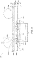
- FIG. 1 illustrates a diagram view of a semiconductor package 100 according to an embodiment of the invention.
- the semiconductor package 100 includes a substrate 110, a first insulation layer 120, a second insulation layer 125, at least one conductive pad 130, at least one conductive trace 140, an encapsulation 150 and at least one contact 160.
- the semiconductor package 100 is, for example, Wafer Level Chip Scale Packaging (WLCSP).
- WLCSP Wafer Level Chip Scale Packaging
- the first insulation layer 120 is formed on the substrate 110 and has at least one first through hole 120a.
- the conductive pad 130 is formed on the substrate 110 through the first through hole 120a.
- the second insulation layer 125 has a first surface 125u and at least one second through hole 125a, wherein the second through hole 125a extends to the conductive pad 130 from the first surface 125u.
- the conductive trace 140 has a second surface 140u and is connected to the conductive pad 130 through the second through hole 125a.
- the entire of the first surface 125u is in the same level, and the entire of the second surface 140u is in the same level. In other words, the first surface 125u has no step surface (structure), and the second surface 140u has no step surface (structure).
- the entire of the second surface 140u is in the same level, it means that the conductive trace 140 has no concave recessed relative to the second surface 140u of the conductive trace 140, and thus it could have stronger or sufficient strength.
- the first surface 125u is, for example, flat surface
- the second surface 140u is, for example, flat surface
- the substrate 110 is, for example, wafer.
- the conductive component 111 of the substrate 110 could include, for example, at least one metal layer, at least one conductive trace, at least one conductive via and/or at least one transistor electrically connected to the metal layer, the conductive trace and/or the conductive via.
- the first insulation layer 120 includes a first layer 121 and a second layer 122.
- the first layer 121 is formed on the substrate 110, and the second layer 122 is formed on the first layer 121.
- the first through hole 120a passes through the first layer 121 and the second layer 122.
- the first layer 121 is made of a material including, for example, silicon nitride (SiN), and the second layer 122 is made of a material including, for example, oxide.
- the first through hole 120a has a width W1 greater than 5 micrometer ( ⁇ m), or ranging between 5 ⁇ m and 300 ⁇ m, or even greater than 300 ⁇ m, wherein the width W1 is, for example, the dimension in width or diameter. Viewing from a top direction, the first through hole 120a could be circle, polygon, ellipse, etc.
- the second insulation layer 125 cover the first insulation layer 120 and a portion of the conductive pad 130.
- the second insulation layer 125 includes a third layer 1251 and a fourth layer 1252.
- the third layer 1251 cover the first insulation layer 120 and a portion of the conductive pad 130, and the fourth layer 1252 is formed on the third layer 1251.
- the second through hole 125a passes through the third layer 1251 and the fourth layer 125 to expose a portion of the conductive pad 130.
- the third layer 1251 has at least one first hole 1251a
- the fourth layer 1252 has at least one second hole 1252a, wherein the first hole 1251a and the second hole 1252a form the second through hole 125a to expose the conductive pad 130.
- the first hole 1251a and the second hole 1252a could be formed in the same manufacturing process, for example, etching. In the present embodiment, a number of the second through holes 125a extend to the same (or one) conductive pad 130 from the first surface 125u.
- the third layer 1251 could be made of a material including, for example, oxide
- the fourth layer 1252 could be made of a material including, for example, silicon nitride (SiN).
- the second through hole 125a has a width W2.
- the width W2 ranges between 2 ⁇ m and 12 ⁇ m, even less than 2 ⁇ m or greater than 12 ⁇ m, wherein the width W2 is, for example, the dimension in width or diameter.
- the width W2 is small enough, and accordingly it could prevent the extending portion 142 above the connecting portion 141 from forming/generating recess, cavity, concave and/or crack. As a result, the conductive trace 140 has sufficient strength.
- the second through hole 125a could be circle, polygon, ellipse, etc.
- the first surface 125u is an upper surface of the fourth layer 1252, and the third layer 1251 has a third surface 1251u, wherein the third surface 1251u is in the same level.
- the third surface 1251u is, for example, a grinding surface by a process, for example, CMP (Chemical-Mechanical Planarization).
- each conductive pad 130 includes a conductive via 131 and a protrusion layer 132.
- the conductive via 131 is directly formed on the conductive component 111 of the substrate 110 through the first through hole 120a. In other words, there is no physical material between the conductive component 111 and the conductive via 131. In addition, at least one portion of the conductive via 131 could be formed within the first through hole 120a.
- the conductive via 131 has an upper surface 131u which could protrude relative to an upper surface 120u of the first insulation layer 120. In another embodiment, the upper surface 131u could be recessed relative to an upper surface 120u of the first insulation layer 120, or flush with the upper surface 120u of the first insulation layer 120.
- the conductive via 131 fills up the first through hole 120a and could receive or carry a plurality of the connecting portions 141, for example, four connecting portions 141.
- the conductive via 131 has the width W1 formed within the first through hole 120a.
- the conductive via 131 could be circle, polygon, ellipse, etc.
- the protrusion layer 132 connects with the conductive via 131, protrudes relative to the upper surface 131u of the conductive via 131 and extends beyond a lateral surface 131s of the conductive via 131.
- the conductive via 131 and the protrusion layer 132 could be formed in the same manufacture process, for example, sputtering. As a result, the conductive via 131 and the protrusion layer 132 could form an integral structure. In addition, due to sputtering, the protrusion layer 132 has a curved lateral surface 132s connected to the upper surface 131u of the conductive via 131. In addition, the protrusion layer 132 has an opening 132a exposing the conductive via 131, wherein the conductive trace 140 is connected to the conductive via 131 through the opening 132a. In terms of material, the conductive via 131 and the protrusion layer 132 could be made of a material including, for example, aluminum, copper or combination thereof. In addition, viewing from a top direction, the protrusion layer 132 could be a closed-ring or opened-ring exposing the upper surface 131u of the conductive via 131.
- At least one conductive trace 140 is, for example, at least one of a portion of Redistribution Layer (RDL).
- the conductive trace 140 includes at least one connecting portion 141 and an extending portion 142 connected to the at least one connecting portion 141, wherein each connecting portion 141 fills up the corresponding second through hole 125a to be connected with the conductive via 131.
- the conductive trace 140 and the conductive via 131 overlap up and down.
- the whole of the connecting portion 141, a portion of the extending portion 142 and the conductive via 131 overlap up and down.
- the first through hole 120a, the connecting portion 141 and the conductive via 131 overlap up and down.
- the conductive trace 140 could be made of a material including, for example, aluminum, copper or combination thereof.
- the connecting portion 141 filling up the second through hole 125a has the width W2.
- the width W2 of the connecting portion 141 is less than the width W1 of the conductive via 131 formed within the first through hole 120a.
- the conductive trace 140 is directly connected to the conductive pad 130 which is located right above the first through hole 120a.
- the connecting portion 141 of the conductive trace 140 is located right above the first through hole 120a.
- a conductive path P1 among the conductive component 111, the conductive trace 140 and the conductive via 130 is shorter or the shortest (for example, in vertical distance), and thus it could reduce parasitic resistance.
- the molding compound includes, for example, Polybenzoxazole (PBO).
- PBO Polybenzoxazole
- the encapsulation 150 covers the conductive trace 140 and/or and the conductive trace 140.
- the encapsulation 150 has at least one an opening 150a exposing the extending portion 142 of the conductive trace 140.
- the encapsulation 150 could be made of a material including, for example, PBO (Polybenzoxazole) or molding compound material.
- Each contact 160 is physically connected or electrically connected to the conductive trace 140 through the corresponding opening 150a.
- the contact 160 is, for example, solder ball, conductive pillar, etc.
- FIG. 2 illustrates a diagram view of a semiconductor package 200 according to another embodiment of the invention.
- the semiconductor package 200 includes the substrate 110, the first insulation layer 220, the second insulation layer 225, at least one conductive pad 230, at least one conductive trace 240, the encapsulation 150 and at least one contact 160.
- the semiconductor package 200 includes the features similar to or the same as that of the semiconductor package 100 expect that the conductive pad 230 of the semiconductor package 200 receive or carry one connecting portion 141, that is, one connecting portion 141 is connects to one conductive pad 230.
- the first insulation layer 220 has at least one first through hole 220a.
- the first through hole 220a has a width W1' smaller that the width W2 of the first through hole 220a.
- the width W1' of the first through hole 220a is smaller than the width W1 of the first through hole 120a of the semiconductor package 100.
- the width W1' of the first through hole 220a is greater than 5 ⁇ m, or ranges between 5 ⁇ m and 300 ⁇ m, or even is greater than 300 ⁇ m , and the conductive via 131 within the first through hole 220a could receive or carry one connecting portions 141.
- the second insulation layer 225 has at least one second through hole 125a extending to the conductive pad 230 from the first surface 125u of the second insulation layer 225.
- the connecting portion 141 fills up the corresponding second through hole 125a to connect with the conductive via 131 of the conductive pad 230.
- FIG. 3 illustrates a diagram view of a semiconductor package 300 according to another embodiment of the invention.
- the semiconductor package 300 includes the substrate 110, the first insulation layer 220, the second insulation layer 225, at least one conductive pad 230, at least one conductive trace 240, the encapsulation 150 and at least one contact 160.
- the semiconductor package 300 includes the features similar to or the same as that of the semiconductor package 200 expect that a number of the conductive pads 230 of the semiconductor package 300 are disposed adjacently.
- the substrate 110 includes a plurality of the conductive component 111 which are electrically connected with a plurality of the conductive traces 240.
- a number of the conductive pads 230 are disposed adjacently in the semiconductor package 300 while just one conductive pad 230 is disposed in the semiconductor package 200 as shown in FIG. 1 .
- the semiconductor package 300 could provide more I/O ports and/or voltage levels in the same width W1.
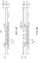
- FIGS. 4A to 4F illustrate manufacturing processes of the semiconductor package 100 of FIG. 1 .
- the substrate 110 is provided, wherein the substrate 110 is, for example, wafer, and the substrate 110 includes at least one conductive component 111, at least one metal layer (not illustrated), at least one conductive trace (not illustrated), at least one conductive via (not illustrated) and/or at least one transistor (not illustrated) electrically connected to the metal layer, the conductive trace and/or the conductive via.
- the first insulation layer 120 including the first layer 121 and the second layer 122 is formed on substrate 110 by using, for example, coating, applying, etc.
- the first insulation layer 120 has at least one first through hole 120a exposing the corresponding conductive component 111.
- the first through hole 120a is formed by using, for example, etching.
- At least one conductive via 131 and at least one protrusion layer 132 are formed within the corresponding first through hole 120a. At least one protrusion layer 132 and at least one conductive via 131 form at least one conductive pad 130.
- the conductive via 131 and the protrusion layer 132 could be formed in the same manufacture process, for example, sputtering, and thus the conductive via 131 and the protrusion layer 132 could form an integral structure. Due to sputtering, the protrusion layer 132 forms the curved lateral surface 132s connected to the upper surface 131u of the conductive via 131.
- the protrusion layer 132 has the opening 132a exposing the conductive via 131, and the conductive trace 140 is connected to the conductive via 131 through the opening 132a.
- the conductive via 131 and the protrusion layer 132 could be made of a material including, for example, aluminum, copper or combination thereof.
- the protrusion layer 132 could be a closed-ring or opened-ring exposing the upper surface 131u of the conductive via 131.
- the protrusion layer 132 connects with the conductive via 131, protrudes relative to the upper surface 131u of the conductive via 131 and extends beyond the lateral surface 131s of the conductive via 131.
- a third layer material 1251' covering the conductive pad 130 and the first insulation layer 120 is formed by using, for example, coating, applying, etc.
- the third layer material 1251' is planarized to form the third surface 1251u of the third layer material 1251' is formed by using, for example, CMP.
- the third surface 1251u is flat surface, for example.
- the third layer material 1251' could be made of a material including, for example, oxide.
- the fourth layer material 1252' covering the third layer material 1251' is formed by using, for example, coating, applying, etc.
- the fourth layer material 1252' and the third layer material 1251' form the second insulation layer material 125'.
- the fourth layer material 1252' could be made of a material including, for example, silicon nitride (SiN).
- the third layer 1251 has at least one first hole 1251a
- the fourth layer 1252 has at least one second hole 1252a, wherein the first hole 1251a and the second hole 1252a form the second through hole 125a.
- the first hole 1251a and the second hole 1252a could be formed in the same manufacturing process, for example, etching.
- a number of the second through holes 125a extend to the same (or one) conductive pad 130 from the first surface 125u.
- At least one conductive trace 140 covering the second insulation layer 125 is formed on the encapsulation 150 by using, for example, sputtering, plating, etc.
- the conductive trace 140 includes at least one connecting portion 141 and an extending portion 142 connected to the at least one connecting portion 141, wherein each connecting portion 141 fills up the corresponding second through hole 125a to be connected with the conductive via 131.
- the conductive trace 140 and the conductive via 131 overlap up and down.
- the whole of the connecting portions 141, a portion of the extending portion 142 and the conductive via 131 overlap up and down.
- the first through hole 120a, the connecting portions 141 and the conductive via 131 overlap up and down.
- the conductive trace 140 could be made of a material including, for example, aluminum, copper or combination thereof.
- the encapsulation 150 covering the conductive trace 140 is formed by using, for example, coating, applying, etc.
- the encapsulation 150 has at least one an opening 150a exposing the extending portion 142 of the conductive trace 140.
- the encapsulation 150 could be made of a material including, for example, PBO (Polybenzoxazole) or molding compound material.
- the contact 160 is, for example, solder ball, conductive pillar, etc.
Landscapes
- Internal Circuitry In Semiconductor Integrated Circuit Devices (AREA)
- Engineering & Computer Science (AREA)
- Manufacturing & Machinery (AREA)
- Encapsulation Of And Coatings For Semiconductor Or Solid State Devices (AREA)
Abstract
Description
- The invention relates to a semiconductor package and a manufacturing method thereof, and more particularly to a semiconductor package and a manufacturing method thereof including a conductive via.
- Conventional semiconductor package includes a conductive via, conductive trace and a substrate including a conductive component, wherein the conductive via electrically connects the conductive trace and the conductive component. The conductive trace generally conforms to shape of a through hole below the conductive trace to form a recess. However, such recess results reduced strength or incomplete structure. Thus, how to make the conductive trace have complete structure has become a prominent task for the industries.
- Thus, how to connect with the semiconductor devices for increasing transmission speed has become a prominent task for the industries.
- In an embodiment of the invention, a semiconductor package is provided. The semiconductor package includes a substrate, a first insulation layer, a conductive pad, a second insulation layer and a conductive trace. The first insulation layer is formed on the substrate and having a first through hole. The conductive pad is formed on the substrate through the first through hole. The second insulation layer has a first surface and a second through hole, wherein the second through hole extends to the conductive pad from the first surface. The conductive trace has a second surface and is connected to the conductive pad through the second through hole. The entire of the first surface is in the same level, and the entire of the second surface is in the same level.
- In another embodiment of the invention, a semiconductor package is provided. The manufacturing method includes the following steps: providing a substrate; forming a first insulation layer on the substrate, wherein the first insulation layer has a first through hole; forming a conductive pad on the substrate through the first through hole; forming a second insulation layer having a first surface and a second through hole, wherein the second through hole extends to the conductive pad from the first surface, wherein the entire of the first surface is in the same level; and forming a conductive trace having a second surface and connected to the conductive pad through the second through hole, wherein the entire of the second surface is in the same level.
- Numerous objects, features and advantages of the invention will be readily apparent upon a reading of the following detailed description of embodiments of the invention when taken in conjunction with the accompanying drawings. However, the drawings employed herein are for the purpose of descriptions and should not be regarded as limiting.
- The above objects and advantages of the invention will become more readily apparent to those ordinarily skilled in the art after reviewing the following detailed description and accompanying drawings, in which:
-
FIG. 1 illustrates a diagram view of a semiconductor package according to an embodiment of the invention. -
FIG. 2 illustrates a diagram view of a semiconductor package according to another embodiment of the invention. -
FIG. 3 illustrates a diagram view of a semiconductor package according to another embodiment of the invention; and -
FIGS. 4A to 4F illustrate manufacturing processes of the semiconductor package ofFIG. 1 . - Referring to
FIG. 1, FIG. 1 illustrates a diagram view of asemiconductor package 100 according to an embodiment of the invention. Thesemiconductor package 100 includes asubstrate 110, afirst insulation layer 120, asecond insulation layer 125, at least oneconductive pad 130, at least oneconductive trace 140, anencapsulation 150 and at least onecontact 160. Thesemiconductor package 100 is, for example, Wafer Level Chip Scale Packaging (WLCSP). - The
first insulation layer 120 is formed on thesubstrate 110 and has at least one first throughhole 120a. Theconductive pad 130 is formed on thesubstrate 110 through the first throughhole 120a. Thesecond insulation layer 125 has afirst surface 125u and at least one second throughhole 125a, wherein the second throughhole 125a extends to theconductive pad 130 from thefirst surface 125u. Theconductive trace 140 has asecond surface 140u and is connected to theconductive pad 130 through the second throughhole 125a. The entire of thefirst surface 125u is in the same level, and the entire of thesecond surface 140u is in the same level. In other words, thefirst surface 125u has no step surface (structure), and thesecond surface 140u has no step surface (structure). In the present embodiment, the entire of thesecond surface 140u is in the same level, it means that theconductive trace 140 has no concave recessed relative to thesecond surface 140u of theconductive trace 140, and thus it could have stronger or sufficient strength. - As shown in
FIG. 1 , thefirst surface 125u is, for example, flat surface, and thesecond surface 140u is, for example, flat surface. - As shown in
FIG. 1 , thesubstrate 110 is, for example, wafer. Theconductive component 111 of thesubstrate 110 could include, for example, at least one metal layer, at least one conductive trace, at least one conductive via and/or at least one transistor electrically connected to the metal layer, the conductive trace and/or the conductive via. - As shown in
FIG. 1 , thefirst insulation layer 120 includes afirst layer 121 and asecond layer 122. Thefirst layer 121 is formed on thesubstrate 110, and thesecond layer 122 is formed on thefirst layer 121. The first throughhole 120a passes through thefirst layer 121 and thesecond layer 122. In addition, thefirst layer 121 is made of a material including, for example, silicon nitride (SiN), and thesecond layer 122 is made of a material including, for example, oxide. In addition, the first throughhole 120a has a width W1 greater than 5 micrometer (µm), or ranging between 5 µm and 300 µm, or even greater than 300 µm, wherein the width W1 is, for example, the dimension in width or diameter. Viewing from a top direction, the first throughhole 120a could be circle, polygon, ellipse, etc. - As shown in
FIG. 1 , thesecond insulation layer 125 cover thefirst insulation layer 120 and a portion of theconductive pad 130. Thesecond insulation layer 125 includes athird layer 1251 and afourth layer 1252. Thethird layer 1251 cover thefirst insulation layer 120 and a portion of theconductive pad 130, and thefourth layer 1252 is formed on thethird layer 1251. The second throughhole 125a passes through thethird layer 1251 and thefourth layer 125 to expose a portion of theconductive pad 130. Furthermore, thethird layer 1251 has at least onefirst hole 1251a, thefourth layer 1252 has at least onesecond hole 1252a, wherein thefirst hole 1251a and thesecond hole 1252a form the second throughhole 125a to expose theconductive pad 130. Thefirst hole 1251a and thesecond hole 1252a could be formed in the same manufacturing process, for example, etching. In the present embodiment, a number of the second throughholes 125a extend to the same (or one)conductive pad 130 from thefirst surface 125u. In addition, thethird layer 1251 could be made of a material including, for example, oxide, and thefourth layer 1252 could be made of a material including, for example, silicon nitride (SiN). - As shown in
FIG. 1 , the second throughhole 125a has a width W2. The width W2 ranges between 2 µm and 12 µm, even less than 2 µm or greater than 12µm, wherein the width W2 is, for example, the dimension in width or diameter. The width W2 is small enough, and accordingly it could prevent the extendingportion 142 above the connectingportion 141 from forming/generating recess, cavity, concave and/or crack. As a result, theconductive trace 140 has sufficient strength. In addition, viewing from a top direction, the second throughhole 125a could be circle, polygon, ellipse, etc. - As shown in
FIG. 1 , thefirst surface 125u is an upper surface of thefourth layer 1252, and thethird layer 1251 has athird surface 1251u, wherein thethird surface 1251u is in the same level. In another embodiment, thethird surface 1251u is, for example, a grinding surface by a process, for example, CMP (Chemical-Mechanical Planarization). - As shown in
FIG. 1 , eachconductive pad 130 includes a conductive via 131 and aprotrusion layer 132. The conductive via 131 is directly formed on theconductive component 111 of thesubstrate 110 through the first throughhole 120a. In other words, there is no physical material between theconductive component 111 and the conductive via 131. In addition, at least one portion of the conductive via 131 could be formed within the first throughhole 120a. The conductive via 131 has anupper surface 131u which could protrude relative to anupper surface 120u of thefirst insulation layer 120. In another embodiment, theupper surface 131u could be recessed relative to anupper surface 120u of thefirst insulation layer 120, or flush with theupper surface 120u of thefirst insulation layer 120. - As shown in
FIG. 1 , the conductive via 131 fills up the first throughhole 120a and could receive or carry a plurality of the connectingportions 141, for example, four connectingportions 141. The conductive via 131 has the width W1 formed within the first throughhole 120a. In addition, viewing from a top direction, the conductive via 131 could be circle, polygon, ellipse, etc. - As shown in
FIG. 1 , theprotrusion layer 132 connects with the conductive via 131, protrudes relative to theupper surface 131u of the conductive via 131 and extends beyond alateral surface 131s of the conductive via 131. - In an embodiment, the conductive via 131 and the
protrusion layer 132 could be formed in the same manufacture process, for example, sputtering. As a result, the conductive via 131 and theprotrusion layer 132 could form an integral structure. In addition, due to sputtering, theprotrusion layer 132 has a curvedlateral surface 132s connected to theupper surface 131u of the conductive via 131. In addition, theprotrusion layer 132 has anopening 132a exposing the conductive via 131, wherein theconductive trace 140 is connected to the conductive via 131 through theopening 132a. In terms of material, the conductive via 131 and theprotrusion layer 132 could be made of a material including, for example, aluminum, copper or combination thereof. In addition, viewing from a top direction, theprotrusion layer 132 could be a closed-ring or opened-ring exposing theupper surface 131u of the conductive via 131. - As shown in
FIG. 1 , at least oneconductive trace 140 is, for example, at least one of a portion of Redistribution Layer (RDL). Theconductive trace 140 includes at least one connectingportion 141 and an extendingportion 142 connected to the at least one connectingportion 141, wherein each connectingportion 141 fills up the corresponding second throughhole 125a to be connected with the conductive via 131. Theconductive trace 140 and the conductive via 131 overlap up and down. Furthermore, the whole of the connectingportion 141, a portion of the extendingportion 142 and the conductive via 131 overlap up and down. In addition, the first throughhole 120a, the connectingportion 141 and the conductive via 131 overlap up and down. In terms of material, theconductive trace 140 could be made of a material including, for example, aluminum, copper or combination thereof. - As shown in
FIG. 1 , the connectingportion 141 filling up the second throughhole 125a has the width W2. The width W2 of the connectingportion 141 is less than the width W1 of the conductive via 131 formed within the first throughhole 120a. - As shown in
FIG. 1 , theconductive trace 140 is directly connected to theconductive pad 130 which is located right above the first throughhole 120a. For example, the connectingportion 141 of theconductive trace 140 is located right above the first throughhole 120a. As a result, a conductive path P1 among theconductive component 111, theconductive trace 140 and the conductive via 130 is shorter or the shortest (for example, in vertical distance), and thus it could reduce parasitic resistance. - As shown in
FIG. 1 , there is no physical layer between theconductive trace 140 and thesecond insulation layer 125. For example, there is no molding compound between theconductive trace 140 and thesecond insulation layer 125. In other words, in the present embodiment, there is no molding compound covering theconductive pad 130 and thesecond insulation layer 125. The molding compound includes, for example, Polybenzoxazole (PBO). Compared to the second throughhole 125a formed on the molding compound, the second throughhole 125a formed on thesecond insulation layer 125 in the present embodiment has the width W2 which could be small. - The
encapsulation 150 covers theconductive trace 140 and/or and theconductive trace 140. Theencapsulation 150 has at least one anopening 150a exposing the extendingportion 142 of theconductive trace 140. Theencapsulation 150 could be made of a material including, for example, PBO (Polybenzoxazole) or molding compound material. Eachcontact 160 is physically connected or electrically connected to theconductive trace 140 through thecorresponding opening 150a. In an embodiment, thecontact 160 is, for example, solder ball, conductive pillar, etc. - Referring to
FIG. 2, FIG. 2 illustrates a diagram view of asemiconductor package 200 according to another embodiment of the invention. Thesemiconductor package 200 includes thesubstrate 110, thefirst insulation layer 220, thesecond insulation layer 225, at least oneconductive pad 230, at least oneconductive trace 240, theencapsulation 150 and at least onecontact 160. - The
semiconductor package 200 includes the features similar to or the same as that of thesemiconductor package 100 expect that theconductive pad 230 of thesemiconductor package 200 receive or carry one connectingportion 141, that is, one connectingportion 141 is connects to oneconductive pad 230. - As shown in
FIG. 2 , in the present embodiment, thefirst insulation layer 220 has at least one first throughhole 220a. The first throughhole 220a has a width W1' smaller that the width W2 of the first throughhole 220a. In the present embodiment, the width W1' of the first throughhole 220a is smaller than the width W1 of the first throughhole 120a of thesemiconductor package 100. The width W1' of the first throughhole 220a is greater than 5 µm, or ranges between 5 µm and 300 µm, or even is greater than 300 µm , and the conductive via 131 within the first throughhole 220a could receive or carry one connectingportions 141. - As shown in
FIG. 2 , thesecond insulation layer 225 has at least one second throughhole 125a extending to theconductive pad 230 from thefirst surface 125u of thesecond insulation layer 225. The connectingportion 141 fills up the corresponding second throughhole 125a to connect with the conductive via 131 of theconductive pad 230. - Referring to
FIG. 3, FIG. 3 illustrates a diagram view of asemiconductor package 300 according to another embodiment of the invention. Thesemiconductor package 300 includes thesubstrate 110, thefirst insulation layer 220, thesecond insulation layer 225, at least oneconductive pad 230, at least oneconductive trace 240, theencapsulation 150 and at least onecontact 160. - The
semiconductor package 300 includes the features similar to or the same as that of thesemiconductor package 200 expect that a number of theconductive pads 230 of thesemiconductor package 300 are disposed adjacently. In addition, as shown inFIG. 3 , thesubstrate 110 includes a plurality of theconductive component 111 which are electrically connected with a plurality of the conductive traces 240. - Furthermore, as shown in
FIG. 3 , in the same width W1, a number of theconductive pads 230 are disposed adjacently in thesemiconductor package 300 while just oneconductive pad 230 is disposed in thesemiconductor package 200 as shown inFIG. 1 . In other words, thesemiconductor package 300 could provide more I/O ports and/or voltage levels in the same width W1. -
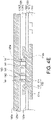
FIGS. 4A to 4F illustrate manufacturing processes of thesemiconductor package 100 ofFIG. 1 . - As illustrated in
FIG. 4A , thesubstrate 110 is provided, wherein thesubstrate 110 is, for example, wafer, and thesubstrate 110 includes at least oneconductive component 111, at least one metal layer (not illustrated), at least one conductive trace (not illustrated), at least one conductive via (not illustrated) and/or at least one transistor (not illustrated) electrically connected to the metal layer, the conductive trace and/or the conductive via. - As illustrated in
FIG. 4A , thefirst insulation layer 120 including thefirst layer 121 and thesecond layer 122 is formed onsubstrate 110 by using, for example, coating, applying, etc. Thefirst insulation layer 120 has at least one first throughhole 120a exposing the correspondingconductive component 111. The first throughhole 120a is formed by using, for example, etching. - As illustrated in
FIG. 4A , at least one conductive via 131 and at least oneprotrusion layer 132 are formed within the corresponding first throughhole 120a. At least oneprotrusion layer 132 and at least one conductive via 131 form at least oneconductive pad 130. In the present embodiment, the conductive via 131 and theprotrusion layer 132 could be formed in the same manufacture process, for example, sputtering, and thus the conductive via 131 and theprotrusion layer 132 could form an integral structure. Due to sputtering, theprotrusion layer 132 forms the curvedlateral surface 132s connected to theupper surface 131u of the conductive via 131. In addition, theprotrusion layer 132 has theopening 132a exposing the conductive via 131, and theconductive trace 140 is connected to the conductive via 131 through theopening 132a. In terms of material, the conductive via 131 and theprotrusion layer 132 could be made of a material including, for example, aluminum, copper or combination thereof. In addition, viewing from a top direction, theprotrusion layer 132 could be a closed-ring or opened-ring exposing theupper surface 131u of the conductive via 131. Theprotrusion layer 132 connects with the conductive via 131, protrudes relative to theupper surface 131u of the conductive via 131 and extends beyond thelateral surface 131s of the conductive via 131. - As illustrated in
FIG. 4B , a third layer material 1251' covering theconductive pad 130 and thefirst insulation layer 120 is formed by using, for example, coating, applying, etc. - As illustrated in
FIG. 4B , the third layer material 1251' is planarized to form thethird surface 1251u of the third layer material 1251' is formed by using, for example, CMP. Thethird surface 1251u is flat surface, for example. In addition, the third layer material 1251' could be made of a material including, for example, oxide. - As illustrated in
FIG. 4C , the fourth layer material 1252' covering the third layer material 1251' is formed by using, for example, coating, applying, etc. The fourth layer material 1252' and the third layer material 1251' form the second insulation layer material 125'. In addition, the fourth layer material 1252' could be made of a material including, for example, silicon nitride (SiN). - As illustrated in
FIG. 4D , at least one second throughhole 125a passing through the third layer material 1251' and the fourth layer material 1252' to form thesecond insulation layer 125 and expose a portion of theconductive pad 130. Furthermore, thethird layer 1251 has at least onefirst hole 1251a, thefourth layer 1252 has at least onesecond hole 1252a, wherein thefirst hole 1251a and thesecond hole 1252a form the second throughhole 125a. Thefirst hole 1251a and thesecond hole 1252a could be formed in the same manufacturing process, for example, etching. In the present embodiment, a number of the second throughholes 125a extend to the same (or one)conductive pad 130 from thefirst surface 125u. - As illustrated in
FIG. 4E , at least oneconductive trace 140 covering thesecond insulation layer 125 is formed on theencapsulation 150 by using, for example, sputtering, plating, etc. Theconductive trace 140 includes at least one connectingportion 141 and an extendingportion 142 connected to the at least one connectingportion 141, wherein each connectingportion 141 fills up the corresponding second throughhole 125a to be connected with the conductive via 131. Theconductive trace 140 and the conductive via 131 overlap up and down. Furthermore, the whole of the connectingportions 141, a portion of the extendingportion 142 and the conductive via 131 overlap up and down. In addition, the first throughhole 120a, the connectingportions 141 and the conductive via 131 overlap up and down. In terms of material, theconductive trace 140 could be made of a material including, for example, aluminum, copper or combination thereof. - As illustrated in
FIG. 4F , theencapsulation 150 covering theconductive trace 140 is formed by using, for example, coating, applying, etc. Theencapsulation 150 has at least one anopening 150a exposing the extendingportion 142 of theconductive trace 140. Theencapsulation 150 could be made of a material including, for example, PBO (Polybenzoxazole) or molding compound material. - Then, at least one
contact 160 physically connected or electrically connected to theconductive trace 140 is formed through thecorresponding opening 150a, as shown inFIG. 1 . In an embodiment, thecontact 160 is, for example, solder ball, conductive pillar, etc. - While the invention has been described in terms of what is presently considered to be the most practical and preferred embodiments, it is to be understood that the invention needs not be limited to the disclosed embodiment. On the contrary, it is intended to cover various modifications and similar arrangements included within the scope of the appended claims which are to be accorded with the broadest interpretation so as to encompass all such modifications and similar structures.
Claims (15)
- A semiconductor package (100, 200, 300), characterized in that the semiconductor package (100, 200, 300) comprises:a substrate (110);a first insulation layer (110, 220) formed on the substrate (110) and having a first through hole (110a, 220a);a conductive pad (130, 230) formed on the substrate (110) through the first through hole (110a, 220a);a second insulation layer (125, 225) having a first surface (125u) and a second through hole (125a), wherein the second through hole (125a) extends to the conductive pad (130, 230) from the first surface (125u); anda conductive trace (140, 240) having a second surface (140u, 240u) and connected to the conductive pad (130, 230) through the second through hole (125a);wherein the entire of the first surface (125u) is in the same level, and the entire of the second surface (140u, 240u) is in the same level.
- The semiconductor package (100, 200, 300) as claimed in claim 1, characterized in that the second insulation layer (125, 225) has a plurality of the second through hole (125a) extending to the same conductive pad (130, 230) from the first surface (125u).
- The semiconductor package (100, 200, 300) as claimed in claim 1 or 2, characterized in that there is no physical layer between the conductive trace (140, 240) and the second insulation layer (125, 225).
- The semiconductor package (100, 200, 300) as claimed in any one of the preceding claims, characterized in that there is no molding compound covering the conductive pad (130, 230) and the second insulation layer (125, 225).
- The semiconductor package (100, 200, 300) as claimed in any one of the preceding claims, characterized in that the second insulation layer (125, 225) comprises a plurality of layers (1251, 1252), one of the layers (1251, 1252) has a third surface (1251u), and the third surface (1251u) is in the same level.
- The semiconductor package (100, 200, 300) as claimed in any one of the preceding claims, characterized in that the conductive trace (140, 240) is directly connected to the conductive pad (130, 230) which is located right above the first through hole (110a, 220a).
- The semiconductor package (100, 200, 300) as claimed in any one of claims 1 to 5, characterized in that the conductive trace (140, 240) comprises a connecting portion (141) and an extending portion (142) connected to the connecting portion (141), the connecting portion (141) is directly connected to the conductive pad (130, 230), and the connecting portion (141) and the conductive pad (130, 230) overlap up and down.
- The semiconductor package (100, 200, 300) as claimed in claim 7, characterized in that the conductive pad (130, 230) comprises:a conductive via (131) formed in the first through hole (110a, 220a); anda protrusion layer (132) connecting with the conductive via (131), protruding relative to an upper surface of the conductive via (131) and extending beyond a lateral surface (131s) of the conductive via (131);wherein the conductive trace (140, 240) is directly connected to the conductive via (131).
- A manufacturing method, characterized in that the manufacturing method comprises:providing a substrate (110);forming a first insulation layer (110, 220) on the substrate (110), wherein the first insulation layer (110, 220) has a first through hole (110a, 220a);forming a conductive pad (130, 230) on the substrate (110) through the first through hole (110a, 220a);forming a second insulation layer (125, 225) having a first surface (125u) and a second through hole (125a), wherein the second through hole (125a) extends to the conductive pad (130, 230) from the first surface (125u), wherein the entire of the first surface (125u) is in the same level; andforming a conductive trace (140, 240) having a second surface (140u, 240u) and connected to the conductive pad (130, 230) through the second through hole (125a), wherein the entire of the second surface (140u, 240u) is in the same level.
- The manufacturing method as claimed in claim 9, characterized in that step of forming the second insulation layer (125, 225) comprises:forming a third layer covering the conductive pad (130, 230) and the first insulation layer (110, 220); andplanarizing the third layer to form a third surface (1251 u) of the third layer, wherein the third surface (1251u) is flat surface.
- The manufacturing method as claimed in claim 10, characterized in that after step of planarizing the layer, the manufacturing method further comprises:forming a fourth layer to cover the third layer; andforming the second through hole (125a) to pass through the fourth layer and the fourth layer to expose a portion of the conductive pad (130, 230).
- The manufacturing method as claimed in claim 9, 10 or 11, characterized in that in step of forming the conductive trace (140, 240), there is no physical layer between the conductive trace (140, 240) and the second insulation layer (125, 225).
- The manufacturing method as claimed in any one of claims 9 to 12, characterized in that in step of forming the second insulation layer (125, 225), there is no molding compound covering the conductive pad (130, 230) and the second insulation layer (125, 225).
- The manufacturing method as claimed in any one of claims 9 to 13, characterized in that in step of forming the second insulation layer (125, 225), the second insulation layer (125, 225) comprises a plurality of layers, one of the layers has a third surface (1251u), and the third surface (1251u) is in the same level.
- The manufacturing method as claimed in any one of claims 9 to 14, characterized in that in step of forming the conductive trace (140, 240), the conductive trace (140, 240) comprises a connecting portion (141) and an extending portion (142) connected to the connecting portion (141), the connecting portion (141) is directly connected to the conductive pad (130, 230), and the connecting portion (141) and the conductive pad (130, 230) overlap up and down.
Applications Claiming Priority (2)
| Application Number | Priority Date | Filing Date | Title |
|---|---|---|---|
| US202163172127P | 2021-04-08 | 2021-04-08 | |
| US17/580,699 US11935852B2 (en) | 2021-04-08 | 2022-01-21 | Semiconductor package and manufacturing method thereof |
Publications (1)
| Publication Number | Publication Date |
|---|---|
| EP4071804A1 true EP4071804A1 (en) | 2022-10-12 |
Family
ID=80736133
Family Applications (1)
| Application Number | Title | Priority Date | Filing Date |
|---|---|---|---|
| EP22161602.2A Pending EP4071804A1 (en) | 2021-04-08 | 2022-03-11 | Semiconductor package and manufacturing method thereof |
Country Status (4)
| Country | Link |
|---|---|
| US (2) | US11935852B2 (en) |
| EP (1) | EP4071804A1 (en) |
| CN (1) | CN115206924A (en) |
| TW (1) | TWI787092B (en) |
Cited By (1)
| Publication number | Priority date | Publication date | Assignee | Title |
|---|---|---|---|---|
| CN119258264A (en) * | 2024-10-09 | 2025-01-07 | 广东云曌医疗科技有限公司 | A hydrogel wound dressing containing nano-cuttlebone |
Families Citing this family (1)
| Publication number | Priority date | Publication date | Assignee | Title |
|---|---|---|---|---|
| US11935852B2 (en) * | 2021-04-08 | 2024-03-19 | Mediatek Inc. | Semiconductor package and manufacturing method thereof |
Citations (3)
| Publication number | Priority date | Publication date | Assignee | Title |
|---|---|---|---|---|
| WO2017171772A1 (en) * | 2016-03-31 | 2017-10-05 | Intel Corporation | Semiconductor package with programmable signal routing |
| US20200105635A1 (en) * | 2018-09-28 | 2020-04-02 | Taiwan Semiconductor Manufacturing Company, Ltd. | Integrated Circuit Package and Method |
| US20200411461A1 (en) * | 2019-06-25 | 2020-12-31 | Samsung Electro-Mechanics Co., Ltd. | Semiconductor package |
Family Cites Families (12)
| Publication number | Priority date | Publication date | Assignee | Title |
|---|---|---|---|---|
| US6271469B1 (en) * | 1999-11-12 | 2001-08-07 | Intel Corporation | Direct build-up layer on an encapsulated die package |
| US6908841B2 (en) | 2002-09-20 | 2005-06-21 | Infineon Technologies Ag | Support structures for wirebond regions of contact pads over low modulus materials |
| JP5582811B2 (en) * | 2010-02-15 | 2014-09-03 | ラピスセミコンダクタ株式会社 | Semiconductor device and manufacturing method thereof |
| US8492171B2 (en) * | 2011-07-21 | 2013-07-23 | International Business Machines Corporation | Techniques and structures for testing integrated circuits in flip-chip assemblies |
| US9379041B2 (en) * | 2013-12-11 | 2016-06-28 | Taiwan Semiconductor Manufacturing Company, Ltd. | Fan out package structure |
| US9953954B2 (en) * | 2015-12-03 | 2018-04-24 | Mediatek Inc. | Wafer-level chip-scale package with redistribution layer |
| US10998267B2 (en) * | 2016-03-11 | 2021-05-04 | Mediatek Inc. | Wafer-level chip-size package with redistribution layer |
| US10636775B2 (en) * | 2017-10-27 | 2020-04-28 | Taiwan Semiconductor Manufacturing Co., Ltd. | Package structure and manufacturing method thereof |
| US10573602B2 (en) * | 2018-06-22 | 2020-02-25 | Nanya Technology Corporation | Semiconductor device and method of forming the same |
| US10804230B2 (en) * | 2018-10-17 | 2020-10-13 | Taiwan Semiconductor Manufacturing Company Ltd. | Semiconductor package and method of manufacturing the same |
| CN111916354B (en) * | 2019-05-07 | 2022-08-30 | 欣兴电子股份有限公司 | Circuit carrier plate and manufacturing method thereof |
| US11935852B2 (en) * | 2021-04-08 | 2024-03-19 | Mediatek Inc. | Semiconductor package and manufacturing method thereof |
-
2022
- 2022-01-21 US US17/580,699 patent/US11935852B2/en active Active
- 2022-03-03 TW TW111107732A patent/TWI787092B/en active
- 2022-03-04 CN CN202210210863.6A patent/CN115206924A/en active Pending
- 2022-03-11 EP EP22161602.2A patent/EP4071804A1/en active Pending
-
2024
- 2024-03-11 US US18/601,003 patent/US12438109B2/en active Active
Patent Citations (3)
| Publication number | Priority date | Publication date | Assignee | Title |
|---|---|---|---|---|
| WO2017171772A1 (en) * | 2016-03-31 | 2017-10-05 | Intel Corporation | Semiconductor package with programmable signal routing |
| US20200105635A1 (en) * | 2018-09-28 | 2020-04-02 | Taiwan Semiconductor Manufacturing Company, Ltd. | Integrated Circuit Package and Method |
| US20200411461A1 (en) * | 2019-06-25 | 2020-12-31 | Samsung Electro-Mechanics Co., Ltd. | Semiconductor package |
Cited By (1)
| Publication number | Priority date | Publication date | Assignee | Title |
|---|---|---|---|---|
| CN119258264A (en) * | 2024-10-09 | 2025-01-07 | 广东云曌医疗科技有限公司 | A hydrogel wound dressing containing nano-cuttlebone |
Also Published As
| Publication number | Publication date |
|---|---|
| TWI787092B (en) | 2022-12-11 |
| US20240213194A1 (en) | 2024-06-27 |
| US11935852B2 (en) | 2024-03-19 |
| US20220328433A1 (en) | 2022-10-13 |
| US12438109B2 (en) | 2025-10-07 |
| CN115206924A (en) | 2022-10-18 |
| TW202240816A (en) | 2022-10-16 |
Similar Documents
| Publication | Publication Date | Title |
|---|---|---|
| US10937667B2 (en) | Semiconductor device and method for manufacturing the same | |
| KR100718063B1 (en) | Semiconductor device, circuit board, and electronic instrument | |
| US11348864B2 (en) | Redistribution substrate having redistribution pattern including via seed patterns covering bottom surface and sidewall surface of wiring conductive patterns and semiconductor package including the same | |
| US20030006493A1 (en) | Semiconductor device and manufacturing method thereof | |
| US12438109B2 (en) | Semiconductor package and manufacturing method thereof | |
| US10109665B2 (en) | Semiconductor device and method of fabricating the same | |
| US10121731B2 (en) | Semiconductor device | |
| US12381151B2 (en) | Semiconductor device and semiconductor package including the same | |
| US11373932B2 (en) | Semiconductor packages including through holes and methods of fabricating the same | |
| KR20210053537A (en) | A semiconductor package | |
| US11798872B2 (en) | Interconnection structure and semiconductor package including the same | |
| US20250364489A1 (en) | Semiconductor package | |
| US20050272243A1 (en) | Method of manufacturing semiconductor device | |
| EP4071805A1 (en) | Semiconductor package and manufacturing method thereof | |
| US9646899B2 (en) | Interconnect assemblies with probed bond pads | |
| US20240321792A1 (en) | Semiconductor package | |
| US20250192082A1 (en) | Semiconductor package including stacked chips |
Legal Events
| Date | Code | Title | Description |
|---|---|---|---|
| PUAI | Public reference made under article 153(3) epc to a published international application that has entered the european phase |
Free format text: ORIGINAL CODE: 0009012 |
|
| STAA | Information on the status of an ep patent application or granted ep patent |
Free format text: STATUS: THE APPLICATION HAS BEEN PUBLISHED |
|
| AK | Designated contracting states |
Kind code of ref document: A1 Designated state(s): AL AT BE BG CH CY CZ DE DK EE ES FI FR GB GR HR HU IE IS IT LI LT LU LV MC MK MT NL NO PL PT RO RS SE SI SK SM TR |
|
| STAA | Information on the status of an ep patent application or granted ep patent |
Free format text: STATUS: REQUEST FOR EXAMINATION WAS MADE |
|
| 17P | Request for examination filed |
Effective date: 20230323 |
|
| RBV | Designated contracting states (corrected) |
Designated state(s): AL AT BE BG CH CY CZ DE DK EE ES FI FR GB GR HR HU IE IS IT LI LT LU LV MC MK MT NL NO PL PT RO RS SE SI SK SM TR |
|
| P01 | Opt-out of the competence of the unified patent court (upc) registered |
Effective date: 20230607 |
|
| STAA | Information on the status of an ep patent application or granted ep patent |
Free format text: STATUS: EXAMINATION IS IN PROGRESS |
|
| 17Q | First examination report despatched |
Effective date: 20241008 |
|
| RAP3 | Party data changed (applicant data changed or rights of an application transferred) |
Owner name: MEDIATEK INC. |