EP4071803A1 - Grid array type lead frame package - Google Patents
Grid array type lead frame package Download PDFInfo
- Publication number
- EP4071803A1 EP4071803A1 EP22165514.5A EP22165514A EP4071803A1 EP 4071803 A1 EP4071803 A1 EP 4071803A1 EP 22165514 A EP22165514 A EP 22165514A EP 4071803 A1 EP4071803 A1 EP 4071803A1
- Authority
- EP
- European Patent Office
- Prior art keywords
- bonding fingers
- semiconductor device
- lead frame
- bonding
- fingers
- Prior art date
- Legal status (The legal status is an assumption and is not a legal conclusion. Google has not performed a legal analysis and makes no representation as to the accuracy of the status listed.)
- Withdrawn
Links
Images



Classifications
-
- H—ELECTRICITY
- H10—SEMICONDUCTOR DEVICES; ELECTRIC SOLID-STATE DEVICES NOT OTHERWISE PROVIDED FOR
- H10W—GENERIC PACKAGES, INTERCONNECTIONS, CONNECTORS OR OTHER CONSTRUCTIONAL DETAILS OF DEVICES COVERED BY CLASS H10
- H10W70/00—Package substrates; Interposers; Redistribution layers [RDL]
- H10W70/40—Leadframes
- H10W70/411—Chip-supporting parts, e.g. die pads
- H10W70/415—Leadframe inner leads serving as die pads
-
- H—ELECTRICITY
- H10—SEMICONDUCTOR DEVICES; ELECTRIC SOLID-STATE DEVICES NOT OTHERWISE PROVIDED FOR
- H10W—GENERIC PACKAGES, INTERCONNECTIONS, CONNECTORS OR OTHER CONSTRUCTIONAL DETAILS OF DEVICES COVERED BY CLASS H10
- H10W74/00—Encapsulations, e.g. protective coatings
- H10W74/10—Encapsulations, e.g. protective coatings characterised by their shape or disposition
- H10W74/111—Encapsulations, e.g. protective coatings characterised by their shape or disposition the semiconductor body being completely enclosed
- H10W74/114—Encapsulations, e.g. protective coatings characterised by their shape or disposition the semiconductor body being completely enclosed by a substrate and the encapsulations
- H10W74/117—Encapsulations, e.g. protective coatings characterised by their shape or disposition the semiconductor body being completely enclosed by a substrate and the encapsulations the substrate having spherical bumps for external connection
-
- H—ELECTRICITY
- H10—SEMICONDUCTOR DEVICES; ELECTRIC SOLID-STATE DEVICES NOT OTHERWISE PROVIDED FOR
- H10W—GENERIC PACKAGES, INTERCONNECTIONS, CONNECTORS OR OTHER CONSTRUCTIONAL DETAILS OF DEVICES COVERED BY CLASS H10
- H10W70/00—Package substrates; Interposers; Redistribution layers [RDL]
- H10W70/40—Leadframes
- H10W70/411—Chip-supporting parts, e.g. die pads
-
- H—ELECTRICITY
- H10—SEMICONDUCTOR DEVICES; ELECTRIC SOLID-STATE DEVICES NOT OTHERWISE PROVIDED FOR
- H10W—GENERIC PACKAGES, INTERCONNECTIONS, CONNECTORS OR OTHER CONSTRUCTIONAL DETAILS OF DEVICES COVERED BY CLASS H10
- H10W70/00—Package substrates; Interposers; Redistribution layers [RDL]
- H10W70/40—Leadframes
- H10W70/421—Shapes or dispositions
- H10W70/424—Cross-sectional shapes
-
- H—ELECTRICITY
- H10—SEMICONDUCTOR DEVICES; ELECTRIC SOLID-STATE DEVICES NOT OTHERWISE PROVIDED FOR
- H10W—GENERIC PACKAGES, INTERCONNECTIONS, CONNECTORS OR OTHER CONSTRUCTIONAL DETAILS OF DEVICES COVERED BY CLASS H10
- H10W70/00—Package substrates; Interposers; Redistribution layers [RDL]
- H10W70/40—Leadframes
- H10W70/421—Shapes or dispositions
- H10W70/438—Shapes or dispositions of side rails, e.g. having holes
-
- H—ELECTRICITY
- H10—SEMICONDUCTOR DEVICES; ELECTRIC SOLID-STATE DEVICES NOT OTHERWISE PROVIDED FOR
- H10W—GENERIC PACKAGES, INTERCONNECTIONS, CONNECTORS OR OTHER CONSTRUCTIONAL DETAILS OF DEVICES COVERED BY CLASS H10
- H10W70/00—Package substrates; Interposers; Redistribution layers [RDL]
- H10W70/40—Leadframes
- H10W70/456—Materials
- H10W70/458—Materials of insulating layers on leadframes
-
- H—ELECTRICITY
- H10—SEMICONDUCTOR DEVICES; ELECTRIC SOLID-STATE DEVICES NOT OTHERWISE PROVIDED FOR
- H10W—GENERIC PACKAGES, INTERCONNECTIONS, CONNECTORS OR OTHER CONSTRUCTIONAL DETAILS OF DEVICES COVERED BY CLASS H10
- H10W74/00—Encapsulations, e.g. protective coatings
- H10W74/01—Manufacture or treatment
-
- H—ELECTRICITY
- H10—SEMICONDUCTOR DEVICES; ELECTRIC SOLID-STATE DEVICES NOT OTHERWISE PROVIDED FOR
- H10W—GENERIC PACKAGES, INTERCONNECTIONS, CONNECTORS OR OTHER CONSTRUCTIONAL DETAILS OF DEVICES COVERED BY CLASS H10
- H10W74/00—Encapsulations, e.g. protective coatings
- H10W74/10—Encapsulations, e.g. protective coatings characterised by their shape or disposition
- H10W74/111—Encapsulations, e.g. protective coatings characterised by their shape or disposition the semiconductor body being completely enclosed
-
- H—ELECTRICITY
- H10—SEMICONDUCTOR DEVICES; ELECTRIC SOLID-STATE DEVICES NOT OTHERWISE PROVIDED FOR
- H10W—GENERIC PACKAGES, INTERCONNECTIONS, CONNECTORS OR OTHER CONSTRUCTIONAL DETAILS OF DEVICES COVERED BY CLASS H10
- H10W90/00—Package configurations
- H10W90/811—Multiple chips on leadframes
-
- H—ELECTRICITY
- H10—SEMICONDUCTOR DEVICES; ELECTRIC SOLID-STATE DEVICES NOT OTHERWISE PROVIDED FOR
- H10W—GENERIC PACKAGES, INTERCONNECTIONS, CONNECTORS OR OTHER CONSTRUCTIONAL DETAILS OF DEVICES COVERED BY CLASS H10
- H10W72/00—Interconnections or connectors in packages
- H10W72/071—Connecting or disconnecting
- H10W72/073—Connecting or disconnecting of die-attach connectors
-
- H—ELECTRICITY
- H10—SEMICONDUCTOR DEVICES; ELECTRIC SOLID-STATE DEVICES NOT OTHERWISE PROVIDED FOR
- H10W—GENERIC PACKAGES, INTERCONNECTIONS, CONNECTORS OR OTHER CONSTRUCTIONAL DETAILS OF DEVICES COVERED BY CLASS H10
- H10W72/00—Interconnections or connectors in packages
- H10W72/071—Connecting or disconnecting
- H10W72/075—Connecting or disconnecting of bond wires
-
- H—ELECTRICITY
- H10—SEMICONDUCTOR DEVICES; ELECTRIC SOLID-STATE DEVICES NOT OTHERWISE PROVIDED FOR
- H10W—GENERIC PACKAGES, INTERCONNECTIONS, CONNECTORS OR OTHER CONSTRUCTIONAL DETAILS OF DEVICES COVERED BY CLASS H10
- H10W72/00—Interconnections or connectors in packages
- H10W72/851—Dispositions of multiple connectors or interconnections
- H10W72/874—On different surfaces
- H10W72/884—Die-attach connectors and bond wires
-
- H—ELECTRICITY
- H10—SEMICONDUCTOR DEVICES; ELECTRIC SOLID-STATE DEVICES NOT OTHERWISE PROVIDED FOR
- H10W—GENERIC PACKAGES, INTERCONNECTIONS, CONNECTORS OR OTHER CONSTRUCTIONAL DETAILS OF DEVICES COVERED BY CLASS H10
- H10W74/00—Encapsulations, e.g. protective coatings
Definitions
- the present disclosure relates generally to the field of semiconductor packaging. More particularly, the present disclosure relates to a grid array type lead frame package.
- BGA semiconductor packages utilize as input and output ends a plurality of solder balls mounted at the bottom of a substrate. Not only can the BGA semiconductor package accommodate more numbers of input and output signals, but can be smaller in size than the quad flat semiconductor package.
- One object of the present invention is to provide a three-dimensional (3D) solder ball pad, an improved interconnection structure, and semiconductor package using the same, in order to solve the above-mentioned prior art problems or shortcomings.
- a semiconductor package and a method for forming a semiconductor package according to the invention are defined in the independent claims.
- the dependent claims define preferred embodiments thereof.
- One aspect of the disclosure provides a semiconductor package, preferably a grid array type lead frame package, including a lead frame comprising a plurality of bonding fingers projecting inwardly from a periphery of the lead frame; a semiconductor device mounted on inner ends of the bonding fingers, wherein the semiconductor device comprises an active surface and a plurality of input/output (I/O) pads disposed on the active surface; a plurality of bonding wires extending between the I/O pads and the bonding fingers for transmitting signals from or to the semiconductor device; a molding compound at least partially encapsulating the semiconductor device, the bonding wires, and the bonding fingers; and a solder mask layer attached to a bottom surface of the molding compound and a bottom surface of each of the bonding fingers.
- I/O input/output
- the semiconductor device is secured to top surfaces of the inner ends of the bonding fingers by using an adhesive film.
- spacing between the bonding fingers is filled with the molding compound.
- the bottom surface of the molding compound is flush with the bottom surface of each of the bonding fingers.
- the solder mask layer comprises solder mask openings, which partially expose the bottom surface of each of the bonding fingers, respectively.
- a connecting element is disposed on the bottom surface of each of the bonding fingers within the solder mask opening.
- the connecting element comprises a solder ball or a metal bump.
- a method for forming a semiconductor package preferably a grid array type lead frame package.
- a lead frame comprising a plurality of bonding fingers projecting inwardly from a periphery of the lead frame is prepared.
- a semiconductor device is mounted on inner ends of the bonding fingers, wherein the semiconductor device comprises an active surface and a plurality of input/output (I/O) pads disposed on the active surface.
- Bonding wires extending between the I/O pads and the bonding fingers for transmitting signals from or to the semiconductor device are formed.
- the semiconductor device, the bonding wires, and the bonding fingers are at least partially encapsulated with a molding compound.
- a solder mask layer is formed on a bottom surface of the molding compound and a bottom surface of each of the bonding fingers.
- the semiconductor device is secured to top surfaces of the inner ends of the bonding fingers by using an adhesive film.
- spacing between the bonding fingers is filled with the molding compound.
- the bottom surface of the molding compound is flush with the bottom surface of each of the bonding fingers.
- the solder mask layer comprises solder mask openings, which partially expose the bottom surface of each of the bonding fingers, respectively.
- a connecting element is formed on the bottom surface of each of the bonding fingers within the solder mask opening.
- the connecting element comprises a solder ball or a metal bump.
- FIG. 1 is a schematic, cross-sectional diagram showing an exemplary grid array type lead frame package according to an embodiment of the invention.
- FIG. 2 is a perspective side view of the grid array type lead frame package in FIG. 1 .
- the grid array type lead frame package 1 comprises a semiconductor device 10 such as a semiconductor chip or die mounted on a lead frame 20.
- the lead frame 20 is made from an entire piece of metal such as copper or copper alloys, but is not limited thereto.
- the lead frame 20 comprises coplanar bonding fingers 201 disposed around the semiconductor device 10.
- the bonding fingers 201 extend inwardly from the outer periphery of the rectangular lead frame 20.
- the semiconductor device 10 may be rested on inner ends 201e of the bonding fingers 201, which are positioned underneath the semiconductor device 10.
- the semiconductor device 10 may be secured to the top surfaces of the inner ends 201e of the bonding fingers 201 by using an adhesive film 110.
- the semiconductor device 10 comprises an active surface 10a facing upwardly.
- a plurality of input/output (I/O) pads 101 is disposed on the active surface 10a.
- bonding wires 301 such as copper wires or gold wires extend between the I/O pads 101 and the bonding fingers 201 for transmitting signals from or to the semiconductor device 10.
- the semiconductor device 10, the bonding wires 301, and the bonding fingers 201 are at least partially encapsulated by a molding compound 40.
- the spacing 230 between the bonding fingers 201 is also filled with the molding compound 40.
- a bottom surface 40b of the molding compound 40 is flush with a bottom surface 201b of each of the bonding fingers 201.
- the grid array type lead frame package 1 further comprises a solder mask layer 50 attached to the coplanar bottom surface 40b of the molding compound 40 and the bottom surface 201b of each of the bonding fingers 201.
- the solder mask layer 50 comprises a plurality of solder mask openings 501, which partially expose the bottom surface 201b of each of the bonding fingers 201, respectively.
- a connecting element 502 such as a solder ball or a metal bump may be disposed on the exposed bottom surface 201b of each of the bonding fingers 201within the solder mask opening 501 for further connection with an external circuit.
- a surface layer (not shown) may be provided on the expose the bottom surface 201b of each of the bonding fingers 201.
- the bonding fingers 201 may be treated by plating or depositing solderable materials such as nickel and gold.
- FIG. 3 to FIG. 8 are schematic diagram showing an exemplary method for fabricating a grid array type lead frame package according to an embodiment of the invention.
- a lead frame 20 is provided.
- the lead frame 20 comprises a plurality of bonding fingers 201 projecting inwardly from the periphery of the rectangular shaped lead frame 20.
- the inner ends 201e of the bonding fingers 201 may be used as mechanical support for a semiconductor chip or die to be mounted on the lead frame 20.
- a semiconductor device 10 such as a semiconductor chip or die is secured onto the inner ends 201e of the bonding fingers 201 by using an adhesive film 110.
- the semiconductor device 10 comprises an active surface 10a facing upwardly.
- a plurality of I/O pads 101 is disposed on the active surface 10a.
- the adhesive film 110 may be partially exposed through the gaps between the bonding fingers 201.
- bonding wires 301 such as copper wires or gold wires are provided between the I/O pads 101 and the bonding fingers 201 for transmitting signals from or to the semiconductor device 10.
- a molding process is performed.
- the semiconductor device 10, the bonding wires 301, and the bonding fingers 201 are at least partially encapsulated by a molding compound 40.
- the spacing 230 between the bonding fingers 201 is also filled with the molding compound 40.
- a bottom surface 40b of the molding compound 40 is flush with a bottom surface 201b of each of the bonding fingers 201.
- solder mask layer 50 is then attached to the coplanar bottom surface 40b of the molding compound 40 and the bottom surface 201b of each of the bonding fingers 201.
- the solder mask layer 50 comprises a plurality of solder mask openings 501, which partially expose the bottom surface 201b of each of the bonding fingers 201, respectively.
- the solder mask openings 501 may be formed by using a lithographic process and an etching process.
- a connecting element 502 such as a solder ball or a metal bump may be disposed on the exposed bottom surface 201b of each of the bonding fingers 201within the solder mask opening 501 for further connection with an external circuit.
Landscapes
- Lead Frames For Integrated Circuits (AREA)
- Wire Bonding (AREA)
Abstract
A grid array type lead frame package (1) includes a lead frame (20) having a plurality of bonding fingers (201) projecting inwardly from a periphery of the lead frame (20); a semiconductor device (10) mounted on inner ends (201e) of the bonding fingers (201), wherein the semiconductor device (10) comprises an active surface (10a) and a plurality of input/output, I/O, pads (101) disposed on the active surface (10a); a plurality of bonding wires (301) extending between the I/O pads (101) and the bonding fingers (201) for transmitting signals from or to the semiconductor device (10); a molding compound (40) at least partially encapsulating the semiconductor device (10), the bonding wires (301), and the bonding fingers (201); and a solder mask layer (50) attached to a bottom surface (40b) of the molding compound (40) and a bottom surface (201b) of each of the bonding fingers (201).
Description
- This application claims priorities from
U.S. provisional application No. 63/171,639 filed on April 7, 2021 - The present disclosure relates generally to the field of semiconductor packaging. More particularly, the present disclosure relates to a grid array type lead frame package.
- As known in the art, ball grid array (BGA) semiconductor packages utilize as input and output ends a plurality of solder balls mounted at the bottom of a substrate. Not only can the BGA semiconductor package accommodate more numbers of input and output signals, but can be smaller in size than the quad flat semiconductor package.
- However, one drawback of the BGA package is that the chip carrier substrate with bismaleimide triazine (BT) resin used as substrate material is expensive and the reliability is not satisfactory.
- One object of the present invention is to provide a three-dimensional (3D) solder ball pad, an improved interconnection structure, and semiconductor package using the same, in order to solve the above-mentioned prior art problems or shortcomings. A semiconductor package and a method for forming a semiconductor package according to the invention are defined in the independent claims. The dependent claims define preferred embodiments thereof.
- One aspect of the disclosure provides a semiconductor package, preferably a grid array type lead frame package, including a lead frame comprising a plurality of bonding fingers projecting inwardly from a periphery of the lead frame; a semiconductor device mounted on inner ends of the bonding fingers, wherein the semiconductor device comprises an active surface and a plurality of input/output (I/O) pads disposed on the active surface; a plurality of bonding wires extending between the I/O pads and the bonding fingers for transmitting signals from or to the semiconductor device; a molding compound at least partially encapsulating the semiconductor device, the bonding wires, and the bonding fingers; and a solder mask layer attached to a bottom surface of the molding compound and a bottom surface of each of the bonding fingers.
- Preferably, the semiconductor device is secured to top surfaces of the inner ends of the bonding fingers by using an adhesive film.
- Preferably, spacing between the bonding fingers is filled with the molding compound.
- Preferably, the bottom surface of the molding compound is flush with the bottom surface of each of the bonding fingers.
- Preferably, the solder mask layer comprises solder mask openings, which partially expose the bottom surface of each of the bonding fingers, respectively.
- Preferably, a connecting element is disposed on the bottom surface of each of the bonding fingers within the solder mask opening.
- Preferably, the connecting element comprises a solder ball or a metal bump.
- Another aspect of the disclosure provides a method for forming a semiconductor package, preferably a grid array type lead frame package. A lead frame comprising a plurality of bonding fingers projecting inwardly from a periphery of the lead frame is prepared. A semiconductor device is mounted on inner ends of the bonding fingers, wherein the semiconductor device comprises an active surface and a plurality of input/output (I/O) pads disposed on the active surface. Bonding wires extending between the I/O pads and the bonding fingers for transmitting signals from or to the semiconductor device are formed. The semiconductor device, the bonding wires, and the bonding fingers are at least partially encapsulated with a molding compound. A solder mask layer is formed on a bottom surface of the molding compound and a bottom surface of each of the bonding fingers.
- Preferably, the semiconductor device is secured to top surfaces of the inner ends of the bonding fingers by using an adhesive film.
- Preferably, spacing between the bonding fingers is filled with the molding compound.
- Preferably, the bottom surface of the molding compound is flush with the bottom surface of each of the bonding fingers.
- Preferably, the solder mask layer comprises solder mask openings, which partially expose the bottom surface of each of the bonding fingers, respectively.
- Preferably, a connecting element is formed on the bottom surface of each of the bonding fingers within the solder mask opening.
- Preferably, the connecting element comprises a solder ball or a metal bump.
- These and other objectives of the present invention will no doubt become obvious to those of ordinary skill in the art after reading the following detailed description of the preferred embodiment that is illustrated in the various figures and drawings.
- The accompanying drawings are included to provide a further understanding of the invention and are incorporated in and constitute a part of this specification. The drawings illustrate embodiments of the invention and, together with the description, serve to explain the principles of the invention. In the drawings:
-
FIG. 1 is a schematic, cross-sectional diagram showing an exemplary grid array type lead frame package according to an embodiment of the invention; -
FIG. 2 is a perspective side view of the grid array type lead frame package inFIG. 1 ; and -
FIG. 3 to FIG. 8 are schematic diagram showing an exemplary method for fabricating a grid array type lead frame package according to an embodiment of the invention. - In the following detailed description of embodiments of the invention, reference is made to the accompanying drawings, which form a part hereof, and in which is shown by way of illustration specific preferred embodiments in which the disclosure may be practiced.
- These embodiments are described in sufficient detail to enable those skilled in the art to practice them, and it is to be understood that other embodiments may be utilized and that mechanical, chemical, electrical, and procedural changes may be made without departing from the scope of the present disclosure. The following detailed description is, therefore, not to be taken in a limiting sense, and the scope of embodiments of the present invention is defined only by the appended claims.
- It will be understood that when an element or layer is referred to as being "on", "connected to" or "coupled to" another element or layer, it can be directly on, connected or coupled to the other element or layer or intervening elements or layers may be present. In contrast, when an element is referred to as being "directly on," "directly connected to" or "directly coupled to" another element or layer, there are no intervening elements or layers present. Like numbers refer to like elements throughout. As used herein, the term "and/or" includes any and all combinations of one or more of the associated listed items.
- Please refer to
FIG. 1 and FIG. 2. FIG. 1 is a schematic, cross-sectional diagram showing an exemplary grid array type lead frame package according to an embodiment of the invention.FIG. 2 is a perspective side view of the grid array type lead frame package inFIG. 1 . As shown inFIG. 1 and FIG. 2 , the grid array typelead frame package 1 comprises asemiconductor device 10 such as a semiconductor chip or die mounted on alead frame 20. Thelead frame 20 is made from an entire piece of metal such as copper or copper alloys, but is not limited thereto. - Preferably, the
lead frame 20 comprisescoplanar bonding fingers 201 disposed around thesemiconductor device 10. Preferably, thebonding fingers 201 extend inwardly from the outer periphery of therectangular lead frame 20. Preferably, thesemiconductor device 10 may be rested oninner ends 201e of thebonding fingers 201, which are positioned underneath thesemiconductor device 10. Preferably, for example, thesemiconductor device 10 may be secured to the top surfaces of theinner ends 201e of thebonding fingers 201 by using anadhesive film 110. - Preferably, the
semiconductor device 10 comprises anactive surface 10a facing upwardly. Preferably, a plurality of input/output (I/O)pads 101 is disposed on theactive surface 10a. Preferably,bonding wires 301 such as copper wires or gold wires extend between the I/O pads 101 and thebonding fingers 201 for transmitting signals from or to thesemiconductor device 10. Preferably, thesemiconductor device 10, thebonding wires 301, and thebonding fingers 201 are at least partially encapsulated by amolding compound 40. Preferably, thespacing 230 between the bondingfingers 201 is also filled with themolding compound 40. Preferably, abottom surface 40b of themolding compound 40 is flush with abottom surface 201b of each of thebonding fingers 201. - Preferably, the grid array type
lead frame package 1 further comprises asolder mask layer 50 attached to thecoplanar bottom surface 40b of themolding compound 40 and thebottom surface 201b of each of thebonding fingers 201. Preferably, thesolder mask layer 50 comprises a plurality ofsolder mask openings 501, which partially expose thebottom surface 201b of each of thebonding fingers 201, respectively. Preferably, a connectingelement 502 such as a solder ball or a metal bump may be disposed on the exposedbottom surface 201b of each of the bonding fingers 201within the solder mask opening 501 for further connection with an external circuit. - Preferably, a surface layer (not shown) may be provided on the expose the
bottom surface 201b of each of thebonding fingers 201. Further, it is understood that thebonding fingers 201 may be treated by plating or depositing solderable materials such as nickel and gold. -
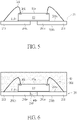
FIG. 3 to FIG. 8 are schematic diagram showing an exemplary method for fabricating a grid array type lead frame package according to an embodiment of the invention. As shown inFIG. 3 , alead frame 20 is provided. Thelead frame 20 comprises a plurality ofbonding fingers 201 projecting inwardly from the periphery of the rectangular shapedlead frame 20. Preferably, the inner ends 201e of thebonding fingers 201 may be used as mechanical support for a semiconductor chip or die to be mounted on thelead frame 20. - As shown in
FIG. 4 , asemiconductor device 10 such as a semiconductor chip or die is secured onto the inner ends 201e of thebonding fingers 201 by using anadhesive film 110. Preferably, thesemiconductor device 10 comprises anactive surface 10a facing upwardly. Preferably, a plurality of I/O pads 101 is disposed on theactive surface 10a. Preferably, at this point, theadhesive film 110 may be partially exposed through the gaps between the bondingfingers 201. - As shown in
FIG. 5 ,bonding wires 301 such as copper wires or gold wires are provided between the I/O pads 101 and thebonding fingers 201 for transmitting signals from or to thesemiconductor device 10. - As shown in
FIG. 6 , a molding process is performed. Thesemiconductor device 10, thebonding wires 301, and thebonding fingers 201 are at least partially encapsulated by amolding compound 40. Preferably, the spacing 230 between the bondingfingers 201 is also filled with themolding compound 40. Preferably, abottom surface 40b of themolding compound 40 is flush with abottom surface 201b of each of thebonding fingers 201. - As shown in
FIG. 7 , asolder mask layer 50 is then attached to the coplanarbottom surface 40b of themolding compound 40 and thebottom surface 201b of each of thebonding fingers 201. Preferably, thesolder mask layer 50 comprises a plurality ofsolder mask openings 501, which partially expose thebottom surface 201b of each of thebonding fingers 201, respectively. Preferably, thesolder mask openings 501 may be formed by using a lithographic process and an etching process. - As shown in
FIG. 8 , a connectingelement 502 such as a solder ball or a metal bump may be disposed on the exposedbottom surface 201b of each of the bonding fingers 201within thesolder mask opening 501 for further connection with an external circuit. - Those skilled in the art will readily observe that numerous modifications and alterations of the device and method may be made while retaining the teachings of the invention. Accordingly, the above disclosure should be construed as limited only by the metes and bounds of the appended claims.
Claims (11)
- A semiconductor package (1), comprising:a lead frame (20) comprising a plurality of bonding fingers (201) projecting inwardly from a periphery of the lead frame (20);a semiconductor device (10) mounted on inner ends (201e) of the bonding fingers (201), wherein the semiconductor device (10) comprises an active surface (10a) and a plurality of input/output, in the following also referred to as I/O, pads (101) disposed on the active surface (10a);a plurality of bonding wires (301) extending between the I/O pads (101) and the bonding fingers (201) for transmitting signals from or to the semiconductor device (10);a molding compound (40) at least partially encapsulating the semiconductor device (10), the bonding wires (301), and the bonding fingers (201); anda solder mask layer (50) attached to a bottom surface (40b) of the molding compound (40) and a bottom surface (201b) of each of the bonding fingers (201).
- A method for forming a semiconductor package (1), comprising:providing a lead frame (20) comprising a plurality of bonding fingers (201) projecting inwardly from a periphery of the lead frame (20);mounting a semiconductor device (10) on inner ends (201e) of the bonding fingers (201), wherein the semiconductor device (10) comprises an active surface (10a) and a plurality of input/output, in the following also referred to as I/O, pads (101) disposed on the active surface (10a);forming bonding wires (301) extending between the I/O pads (101) and the bonding fingers (201) for transmitting signals from or to the semiconductor device (10);at least partially encapsulating the semiconductor device (10), the bonding wires (301), and the bonding fingers (201) with a molding compound (40); andforming a solder mask layer (50) on a bottom surface (40b) of the molding compound (40) and a bottom surface (201b) of each of the bonding fingers (201).
- The semiconductor package (1) according to claim 1, or the method according to claim 2, wherein the semiconductor device (10) is secured to top surfaces of the inner ends (201e) of the bonding fingers by using an adhesive film (110).
- The semiconductor package (1) according to claim 1 or 3, or the method according to claim 2 or 3, wherein spacing (230) between the bonding fingers (201) is filled with the molding compound (40).
- The semiconductor package (1) according to claim 1, 3 or 4, or the method according to any one of claims 2 to 4, wherein the bottom surface (40b) of the molding compound (40) is flush with the bottom surface (201b) of each of the bonding fingers (201).
- The semiconductor package (1) according to any one of claims 1 and 3 to 5, or the method according to any one of claims 2 to 5, wherein the solder mask layer (50) comprises solder mask openings (501), which partially expose the bottom surface (201b) of each of the bonding fingers (201), respectively.
- The semiconductor package (1) according to any one of claims 1 and 3 to 6, wherein a connecting element (502) is disposed on the bottom surface (201b) of each of the bonding fingers (201) within the solder mask opening (501).
- The method according to any one of claims 2 to 6 further comprising:
forming a connecting element (502) on the bottom surface (201b) of each of the bonding fingers (201) within the solder mask opening (501). - The semiconductor package (1) according to claim 7, or the method according to claim 8, wherein the connecting element (502) comprises a solder ball or a metal bump.
- The semiconductor package (1) according to any one of claims 1, 3 to 7, and 9 is a gride array type lead frame package.
- The method according to any one of claims 2 to 6, 8, and 9, wherein the semiconductor device (1) is a gride array type lead frame package.
Applications Claiming Priority (2)
| Application Number | Priority Date | Filing Date | Title |
|---|---|---|---|
| US202163171639P | 2021-04-07 | 2021-04-07 | |
| US17/706,620 US20220328382A1 (en) | 2021-04-07 | 2022-03-29 | Grid array type lead frame package |
Publications (1)
| Publication Number | Publication Date |
|---|---|
| EP4071803A1 true EP4071803A1 (en) | 2022-10-12 |
Family
ID=80999521
Family Applications (1)
| Application Number | Title | Priority Date | Filing Date |
|---|---|---|---|
| EP22165514.5A Withdrawn EP4071803A1 (en) | 2021-04-07 | 2022-03-30 | Grid array type lead frame package |
Country Status (4)
| Country | Link |
|---|---|
| US (1) | US20220328382A1 (en) |
| EP (1) | EP4071803A1 (en) |
| CN (1) | CN115206921A (en) |
| TW (1) | TW202240822A (en) |
Citations (2)
| Publication number | Priority date | Publication date | Assignee | Title |
|---|---|---|---|---|
| US6246117B1 (en) * | 1998-12-15 | 2001-06-12 | Nec Corporation | Semiconductor device comprised of a ball grid array and an insulating film with preformed land openings |
| US20120025375A1 (en) * | 2010-07-30 | 2012-02-02 | Atmel Corporation | Routable array metal integrated circuit package fabricated using partial etching process |
Family Cites Families (4)
| Publication number | Priority date | Publication date | Assignee | Title |
|---|---|---|---|---|
| JP2007509485A (en) * | 2003-08-14 | 2007-04-12 | アドバンスド インターコネクト テクノロジーズ リミテッド | Semiconductor device package and manufacturing method thereof |
| JP2010245417A (en) * | 2009-04-09 | 2010-10-28 | Renesas Electronics Corp | Semiconductor device and manufacturing method thereof |
| TWI404175B (en) * | 2009-12-25 | 2013-08-01 | 矽品精密工業股份有限公司 | Semiconductor package with electrical connection structure and preparation method thereof |
| US12142549B2 (en) * | 2018-07-03 | 2024-11-12 | Texas Instruments Incorporated | Wafer stencil for controlling die attach material thickness on die |
-
2022
- 2022-03-29 US US17/706,620 patent/US20220328382A1/en not_active Abandoned
- 2022-03-30 EP EP22165514.5A patent/EP4071803A1/en not_active Withdrawn
- 2022-03-31 CN CN202210345890.4A patent/CN115206921A/en not_active Withdrawn
- 2022-04-01 TW TW111112824A patent/TW202240822A/en unknown
Patent Citations (2)
| Publication number | Priority date | Publication date | Assignee | Title |
|---|---|---|---|---|
| US6246117B1 (en) * | 1998-12-15 | 2001-06-12 | Nec Corporation | Semiconductor device comprised of a ball grid array and an insulating film with preformed land openings |
| US20120025375A1 (en) * | 2010-07-30 | 2012-02-02 | Atmel Corporation | Routable array metal integrated circuit package fabricated using partial etching process |
Also Published As
| Publication number | Publication date |
|---|---|
| TW202240822A (en) | 2022-10-16 |
| US20220328382A1 (en) | 2022-10-13 |
| CN115206921A (en) | 2022-10-18 |
Similar Documents
| Publication | Publication Date | Title |
|---|---|---|
| US5508556A (en) | Leaded semiconductor device having accessible power supply pad terminals | |
| US7432583B2 (en) | Leadless leadframe package substitute and stack package | |
| US7719094B2 (en) | Semiconductor package and manufacturing method thereof | |
| EP1855316A1 (en) | Stackable integrated circuit package | |
| US5894107A (en) | Chip-size package (CSP) using a multi-layer laminated lead frame | |
| US20080138934A1 (en) | Method of manufacturing multi-stack package | |
| US20070176269A1 (en) | Multi-chips module package and manufacturing method thereof | |
| JP2007221139A (en) | System for an integrated circuit package system having a die on a base package | |
| US20110248392A1 (en) | Ball-Grid Array Device Having Chip Assembled on Half-Etched metal Leadframe | |
| US7049173B2 (en) | Method for fabricating semiconductor component with chip on board leadframe | |
| US7378298B2 (en) | Method of making stacked die package | |
| US7023076B2 (en) | Multiple chip semiconductor packages | |
| US20110241187A1 (en) | Lead frame with recessed die bond area | |
| TWI566340B (en) | Semiconductor package and method of manufacturing same | |
| KR101474189B1 (en) | Integrated circuit package | |
| US7375435B2 (en) | Chip package structure | |
| US20100148349A1 (en) | Semiconductor Package Having Support Chip And Fabrication Method Thereof | |
| US20020003308A1 (en) | Semiconductor chip package and method for fabricating the same | |
| KR101515777B1 (en) | Method of manufacturing Semiconductor package | |
| KR100673379B1 (en) | Laminated package and its manufacturing method | |
| US20220328382A1 (en) | Grid array type lead frame package | |
| US20070026573A1 (en) | Method of making a stacked die package | |
| KR102233649B1 (en) | Stacked semiconductor package and manufacturing method of the same | |
| KR100470144B1 (en) | Semiconductor chip package with tape circuit board and chip size using it | |
| KR101432486B1 (en) | Method for manufacturing of integrated circuit package |
Legal Events
| Date | Code | Title | Description |
|---|---|---|---|
| PUAI | Public reference made under article 153(3) epc to a published international application that has entered the european phase |
Free format text: ORIGINAL CODE: 0009012 |
|
| STAA | Information on the status of an ep patent application or granted ep patent |
Free format text: STATUS: THE APPLICATION HAS BEEN PUBLISHED |
|
| AK | Designated contracting states |
Kind code of ref document: A1 Designated state(s): AL AT BE BG CH CY CZ DE DK EE ES FI FR GB GR HR HU IE IS IT LI LT LU LV MC MK MT NL NO PL PT RO RS SE SI SK SM TR |
|
| STAA | Information on the status of an ep patent application or granted ep patent |
Free format text: STATUS: THE APPLICATION IS DEEMED TO BE WITHDRAWN |
|
| 18D | Application deemed to be withdrawn |
Effective date: 20230413 |
|
| RAP3 | Party data changed (applicant data changed or rights of an application transferred) |
Owner name: MEDIATEK INC. |