EP4068712A1 - Envelope detector circuit, corresponding receiver circuit and galvanic isolator device - Google Patents
Envelope detector circuit, corresponding receiver circuit and galvanic isolator device Download PDFInfo
- Publication number
- EP4068712A1 EP4068712A1 EP22164899.1A EP22164899A EP4068712A1 EP 4068712 A1 EP4068712 A1 EP 4068712A1 EP 22164899 A EP22164899 A EP 22164899A EP 4068712 A1 EP4068712 A1 EP 4068712A1
- Authority
- EP
- European Patent Office
- Prior art keywords
- sub
- circuit
- node
- coupled
- transistor
- Prior art date
- Legal status (The legal status is an assumption and is not a legal conclusion. Google has not performed a legal analysis and makes no representation as to the accuracy of the status listed.)
- Granted
Links
Images

Classifications
-
- H—ELECTRICITY
- H04—ELECTRIC COMMUNICATION TECHNIQUE
- H04L—TRANSMISSION OF DIGITAL INFORMATION, e.g. TELEGRAPHIC COMMUNICATION
- H04L25/00—Baseband systems
- H04L25/02—Details ; arrangements for supplying electrical power along data transmission lines
- H04L25/0264—Arrangements for coupling to transmission lines
- H04L25/0266—Arrangements for providing Galvanic isolation, e.g. by means of magnetic or capacitive coupling
- H04L25/0268—Arrangements for providing Galvanic isolation, e.g. by means of magnetic or capacitive coupling with modulation and subsequent demodulation
-
- H—ELECTRICITY
- H03—ELECTRONIC CIRCUITRY
- H03F—AMPLIFIERS
- H03F1/00—Details of amplifiers with only discharge tubes, only semiconductor devices or only unspecified devices as amplifying elements
- H03F1/02—Modifications of amplifiers to raise the efficiency, e.g. gliding Class A stages, use of an auxiliary oscillation
- H03F1/0205—Modifications of amplifiers to raise the efficiency, e.g. gliding Class A stages, use of an auxiliary oscillation in transistor amplifiers
- H03F1/0211—Modifications of amplifiers to raise the efficiency, e.g. gliding Class A stages, use of an auxiliary oscillation in transistor amplifiers with control of the supply voltage or current
- H03F1/0216—Continuous control
- H03F1/0233—Continuous control by using a signal derived from the output signal, e.g. bootstrapping the voltage supply
-
- H—ELECTRICITY
- H03—ELECTRONIC CIRCUITRY
- H03F—AMPLIFIERS
- H03F3/00—Amplifiers with only discharge tubes or only semiconductor devices as amplifying elements
- H03F3/189—High-frequency amplifiers, e.g. radio frequency amplifiers
- H03F3/19—High-frequency amplifiers, e.g. radio frequency amplifiers with semiconductor devices only
-
- H—ELECTRICITY
- H04—ELECTRIC COMMUNICATION TECHNIQUE
- H04B—TRANSMISSION
- H04B1/00—Details of transmission systems, not covered by a single one of groups H04B3/00 - H04B13/00; Details of transmission systems not characterised by the medium used for transmission
- H04B1/38—Transceivers, i.e. devices in which transmitter and receiver form a structural unit and in which at least one part is used for functions of transmitting and receiving
- H04B1/40—Circuits
-
- H—ELECTRICITY
- H04—ELECTRIC COMMUNICATION TECHNIQUE
- H04L—TRANSMISSION OF DIGITAL INFORMATION, e.g. TELEGRAPHIC COMMUNICATION
- H04L25/00—Baseband systems
- H04L25/02—Details ; arrangements for supplying electrical power along data transmission lines
- H04L25/0264—Arrangements for coupling to transmission lines
- H04L25/0272—Arrangements for coupling to multiple lines, e.g. for differential transmission
-
- H—ELECTRICITY
- H04—ELECTRIC COMMUNICATION TECHNIQUE
- H04L—TRANSMISSION OF DIGITAL INFORMATION, e.g. TELEGRAPHIC COMMUNICATION
- H04L25/00—Baseband systems
- H04L25/38—Synchronous or start-stop systems, e.g. for Baudot code
- H04L25/40—Transmitting circuits; Receiving circuits
- H04L25/49—Transmitting circuits; Receiving circuits using code conversion at the transmitter; using predistortion; using insertion of idle bits for obtaining a desired frequency spectrum; using three or more amplitude levels ; Baseband coding techniques specific to data transmission systems
- H04L25/4902—Pulse width modulation; Pulse position modulation
-
- H—ELECTRICITY
- H03—ELECTRONIC CIRCUITRY
- H03F—AMPLIFIERS
- H03F2200/00—Indexing scheme relating to amplifiers
- H03F2200/105—A non-specified detector of the power of a signal being used in an amplifying circuit
-
- H—ELECTRICITY
- H03—ELECTRONIC CIRCUITRY
- H03F—AMPLIFIERS
- H03F2200/00—Indexing scheme relating to amplifiers
- H03F2200/451—Indexing scheme relating to amplifiers the amplifier being a radio frequency amplifier
Definitions
- the description relates to envelope detector circuits and related devices.
- Galvanic isolation is a desirable feature in certain automotive applications (e.g., driver devices for electric and hybrid vehicles), in the industrial environment (e.g., motor control, automation, and the like), in medical equipment, in consumer products (e.g., home appliances), in gate drivers for power devices (e.g., power MOS, SiC or GaN devices), and even in communication networks.
- a galvanic isolator facilitates data transfer across a galvanic barrier and allows bidirectional communication between two isolated interfaces.
- Figure 3 (also known from document Ragonese et al. cited previously) is a simplified circuit block diagram exemplary of an isolated data transfer channel of an isolated system (e.g., 10 or 20), and Figure 4 is exemplary of possible time behavior of electrical signals in the system.
- the signal PWM IN may comprise periods with a low duty-cycle (e.g., 25% or less) to encode a "0" bit value, and periods with a high duty-cycle (e.g., 75% or more) to encode a "1" bit value, as exemplified in Figure 4 .
- the transmission front-end circuit 304 1 modulates the amplitude of a radio-frequency carrier wave as a function of the PWM signal PWM IN (e.g., applying ASK modulation, in particular OOK modulation) to produce the transmission signal S RF which is then transmitted by a transmitting antenna 204 1 coupled to the transmission front-end circuit 304 1 .
- the receiving chip 200 2 on the other side of the isolation barrier 306, comprises a reception front-end circuit 304 2 coupled to the receiving antenna 204 2 to receive the transmission signal S RF therefrom.
- the reception front-end circuit 304 2 comprises an envelope detector circuit which detects the envelope of the transmission signal S RF to produce an output PWM signal PWM OUT .
- the output PWM signal PWM OUT is provided to a base-band interface 302 2 for data demodulation (e.g., a PWM demodulator circuit), which produces an output digital signal OUT at an output pin 300 2 .
- the front-end circuit 304 2 in the receiving chip 200 2 is configured to rectify (e.g., perform envelope detection) and amplify the low-level radio-frequency signal S RF received so as to convert it into a PWM low frequency signal PWM OUT , thereby allowing inter-chip data communication with two micro-antennas which transmit and receive, respectively, a carrier signal.
- such an object can be achieved by means of a circuit (e.g., an envelope detection circuit) having the features set forth in the claims that follow.
- a circuit e.g., an envelope detection circuit
- One or more embodiments may relate to a corresponding receiver circuit.
- Figure 7 is a circuit diagram exemplary of a twostage envelope detector circuit 70 suitable for use in an amplitude-shift keying (ASK) detector.
- ASK amplitude-shift keying
- the envelope detector circuit 70 may comprise an input stage 71 and an output stage 72.
- the input stage 71 may comprise an input differential pair comprising two transistors (e.g., n-channel MOS transistors) M 1 and M 2 .
- the input radio-frequency signal S RF may be applied between the (gate) control terminals of the two transistors M 1 and M 2 of the differential pair.
- the transistors M 1 , M 2 may have their source terminals coupled to a reference voltage node GND and their drain terminals coupled to a common intermediate node 710.
- the input stage 71 may comprise a load coupled between the common intermediate node 710 and a supply node which provides a supply voltage V CC .
- the load may comprise an active (e.g., self-biased) load including a transistor M 3 and a low-pass filter R F , C F .
- the transistor M 3 e.g., a p-channel MOS transistor
- the transistor M 3 may have its current path arranged between the common intermediate node 710 and the supply node V CC .
- the low-pass filter may comprise a resistive element (e.g., a resistor R F ) coupled between the common intermediate node 710 and the (gate) control terminal of the transistor M 3 , and a capacitive element (e.g., a capacitor C F ) coupled between the (gate) control terminal of the transistor M 3 and the supply node V CC .
- a resistive element e.g., a resistor R F
- C F capacitive element
- the output stage 72 may comprise a common source or common emitter arrangement including a transistor M 4 and a resistive load R L , the transistor M 4 and the resistive load R L being coupled in series between the supply node V cc and the reference voltage node GND.
- the transistor M 4 may have a (gate) control terminal coupled to the common intermediate node 710 (acting as the output node of the first stage 71) .
- An output node 720 intermediate the transistor M 4 and the resistive load R L may provide the envelope output signal ENV OUT .
- the transistor M 4 may be a p-channel MOS transistor having a source terminal coupled to the supply node V CC and a drain terminal coupled to the output node 720, and the resistive load R L may be coupled between the drain terminal of transistor M 4 and the reference voltage node GND.
- an envelope detector circuit 70 as exemplified in Figure 7 , the (on-off) modulated differential input signal S RF is first rectified and then amplified to produce an envelope signal ENV OUT .
- the output node 720 of the envelope detector circuit 70 may be coupled to a comparator circuit (not visible in the Figures annexed herein) so that the envelope signal ENV OUT is converted into a single-ended rail-to-rail PWM data signal PWM OUT .
- an envelope detector circuit as exemplified in Figure 7 may require an external component (e.g., an external capacitor C F ).
- One or more embodiments may thus relate to an improved envelope detector circuit suitable for use (also) at low data rates, as exemplified in Figure 8 , which is a circuit diagram exemplary of a three-stage envelope detector circuit 80 suitable for use in an amplitude-shift keying (ASK) detector.
- ASK amplitude-shift keying
- the envelope detector circuit 80 may comprise an input stage 81, an intermediate stage 82 and an output stage 83.
- the input stage 81 may comprise an input differential pair comprising two transistors (e.g., n-channel MOS transistors) M 1 and M 2 .
- the input radio-frequency signal S RF may be applied between the (gate or base) control terminals of the two transistors M 1 and M 2 of the differential pair.
- the transistors M 1 , M 2 may have their source or emitter terminals coupled to a reference voltage node GND and their drain or collector terminals coupled to a common intermediate node 810.
- the input stage 81 may further comprise a load coupled between the common intermediate node 810 and a supply node providing a supply voltage V CC .
- the load may comprise an active (e.g., self-biased) load including a transistor M 3 and a low-pass filter R F , C F .
- the transistor M 3 e.g., a p-channel MOS transistor
- the transistor M 3 may have its current path arranged between the common intermediate node 810 and the supply node V CC .
- the low-pass filter may comprise a resistive element (e.g., a resistor R F ) coupled between the common intermediate node 810 and the (gate or base) control terminal of the transistor M 3 , and a capacitive element (e.g., a capacitor C F ) coupled between the (gate or base) control terminal of the transistor M 3 and the supply node V CC .
- a resistive element e.g., a resistor R F
- C F capacitive element
- the input stage 81 may comprise a resistive element R L1 coupled in parallel to the active load, e.g., coupled between the common intermediate node 810 and the supply node V CC .
- Arranging a further resistive element R L1 in the input stage 81 provides a further degree of freedom in the design of the envelope detector circuit 80, so that the resistive element R F can be set (e.g., dimensioned) to reduce the loop gain-bandwidth product f GBW , which in turn facilitates implementing the capacitive element C F as an integrated component, while R L1 can be set (e.g., dimensioned) so as to determine the gain and output pole frequency of the input stage 81, thus mitigating (e.g., avoiding) edge distortions on the output PWM signal.
- the intermediate stage 82 may comprise a current matching circuit arrangement.
- the intermediate stage 82 may comprise a transistor M 4 (e.g., a p-channel MOS transistor) having a current path arranged between the supply node Vcc and a bias source 822, and a control (gate or base) terminal coupled to the intermediate node 810 of the input stage 81.
- a current I 4 flows through the transistor M 4 .
- the transistor M 4 may have a source or emitter terminal coupled to the supply node Vcc and a drain or collector terminal coupled to a further intermediate node 820, and the bias source 822 may comprise a current generator arranged between the intermediate node 820 and the reference voltage node GND to sink a bias current I b from the intermediate node 820 towards the reference voltage node GND.
- the intermediate stage 82 may comprise a resistive element R L2 coupled in parallel to the current path of transistor M 4 , e.g., coupled between the intermediate node 820 and the supply node V CC .
- Arranging a resistive element R L2 in the intermediate stage 82 facilitates restoring the matching conditions between the first stage 81 (transistor M 3 and resistance R L1 ) and the second stage 82 (transistor M 4 and resistance R L2 ), thus improving the accuracy in the bias current I 5 of the output stage 83.
- the output stage 83 may comprise an amplifier stage, e.g., a folded amplifier stage.
- the output stage 83 may comprise a current mirror arrangement comprising a first transistor M 5 (e.g., a p-channel MOS transistor) and a second transistor M 6 (e.g., a p-channel MOS transistor).
- the second transistor M 6 may be arranged in series to an output load R L3 (e.g., a resistive load) between the supply node V CC and the reference voltage node GND, so that a copy of current I 5 flows through M 6 and R L3 , thereby providing a single-ended output signal ENV OUT at the node 830 intermediate the transistor M 6 and the load R L3 .
- R L3 e.g., a resistive load
- the folded amplifier comprising transistors M 5 and M 6 allows increasing the resistance value of the load R L3 and therefore the value of the second stage gain, insofar as the unipolar output signal ENV OUT becomes a positive voltage.
- the output bias voltage can be set to a value close to V CC .
- V CC 3.5
- the resistance R L3 may be twice as big as the output load of a traditional configuration (e.g., R L in Figure 7 ), thereby providing an additional gain of about 6 dB.
- the output node 830 of the envelope detector circuit 80 may be coupled to a comparator circuit (not visible in the Figures annexed herein) so that the envelope signal ENV OUT is converted into a single-ended rail-to-rail PWM data signal PWM OUT .
- One or more embodiments may be applied in a package-scale galvanic isolator device (e.g., as illustrated in Figure 2 ), where galvanic isolation can be implemented without using specific high voltage components, the inter-chip communication channel can be implemented by means of a wireless radio-frequency transmission, and appropriately choosing the distance between the two chips facilitates achieving high isolation rating (e.g., 10 to 12 kV for reinforced isolation) and/or higher common mode transient immunity, CMTI (e.g., higher than 100 kV).
- high isolation rating e.g. 10 to 12 kV for reinforced isolation
- CMTI common mode transient immunity
- bipolar (BJT) technology can also be adopted as implementation technology for one or more embodiments, provided that it includes complementary transistors.
- One or more embodiments may thus provide an envelope detector circuit which can be fully integrated in a single chip (also) for use at low data rates, e.g., without using passive discrete components to operate the circuit at low data rates.
- envelope detector circuits may operate at frequencies lower than 1 MHz (e.g., in certain applications such as gate driver for motor control).
- One or more embodiments may additionally provide one or more of the following advantages: high immunity to common mode transients, low current consumption, high gain, and low cost.
- a circuit may comprise a rectifier stage (e.g., 81) including a differential input transistor pair (e.g., M 1 , M 2 ) coupled between a reference voltage node (e.g., GND) and an intermediate node (e.g., 810), and a load (e.g., M 3 , R F , C F ) coupled between the intermediate node and a supply voltage node (e.g., V CC ) .
- the differential input transistor pair may be configured to receive a radio-frequency amplitude modulated signal (e.g., S RF+ , S RF- ) .
- a rectified signal indicative of an envelope of the radio-frequency amplitude modulated signal may be produced at the intermediate node.
- the circuit may comprise an amplifier stage (e.g., 82; 83) coupled to the intermediate node to receive the rectified signal and configured to produce at an output node (e.g., 830) an amplified rectified signal (e.g., ENV OUT ) indicative of the envelope of the radio-frequency amplitude modulated signal.
- the rectifier stage may further comprise a first resistive element (e.g., R L1 ) coupled between the intermediate node and the supply voltage node in parallel to the load.
- the load may comprise an active load including a load transistor (e.g., M 3 ) and a low-pass circuit arrangement (e.g., R F , C F ).
- a load transistor e.g., M 3
- a low-pass circuit arrangement e.g., R F , C F
- the active load may comprise the load transistor having a current path coupled between the intermediate node and the supply voltage node, a second resistive element (e.g., R F ) coupled between the intermediate node and a control terminal of the load transistor, and a capacitive element (e.g., C F ) coupled between the control terminal of the load transistor and the supply voltage node.
- a second resistive element e.g., R F
- C F capacitive element
- the first resistive element may have a resistance value in the range of 25 k ⁇ to 50 k ⁇
- the second resistive element may have a resistance value in the range of 1 M ⁇ to 3 M ⁇ .
- the first resistive element may be sized to correctly polarize the transistors M 1 , M 2 and together with the biasing current (e.g., 2*I d1,2 where I d is the current flowing through one of the transistors M 1 , M 2 ) it may define the gain of the first stage. For instance, an amplitude gain in the range of 2 to 3 may be obtained.
- the capacitive element may have a capacitance value in the range of 50 pF to 150 pF.
- the differential input transistor pair may comprise a first input transistor (e.g., M 1 ) and a second input transistor (e.g., M 2 ) having the current paths therethrough arranged in parallel between the reference voltage node and the intermediate node, and the control terminals of the first input transistor and the second input transistor may be configured to receive the radio-frequency amplitude modulated signal therebetween.
- M 1 first input transistor
- M 2 second input transistor
- the amplifier stage may comprise an output transistor (e.g., M 6 ) arranged in a common source or common emitter configuration and an output load (e.g., R L3 ) coupled between a drain or collector terminal of the output transistor and the reference voltage node, and the output node may be intermediate the drain or collector terminal of the output transistor and the output load.
- an output transistor e.g., M 6
- an output load e.g., R L3
- the amplifier stage may comprise:
- control terminal of the current-mirroring transistor may be coupled to a control terminal of the output transistor.
- the circuit may comprise a current-matching resistive element (e.g., R L2 ) coupled between the supply voltage node and the current control node.
- a current-matching resistive element e.g., R L2
- the current-matching resistive element may have a resistance value in the range of 25 k ⁇ to 50 k ⁇ .
- the current-matching resistive element may be sized to correctly polarize the transistor M 4 and together with the biasing current I b it may define the gain of the second stage.
- a receiver circuit (e.g., 200 2 ) may comprise:
- an isolator device may comprise a transmitter circuit (e.g., 200 1 ) configured to transmit a radio-frequency amplitude modulated signal, and a receiver circuit according to one or more embodiments, and the transmitter circuit and the receiver circuit may be isolated by a galvanic isolation barrier (e.g., 306).
- a galvanic isolation barrier e.g., 306
- the transmitter circuit and the receiver circuit may be provided as separate chips arranged on respective electrically-isolated die pads (e.g., 202 1 , 202 2 ), and the isolator device may further comprise a molded package (e.g., 203) providing the galvanic isolation barrier.
Landscapes
- Engineering & Computer Science (AREA)
- Power Engineering (AREA)
- Computer Networks & Wireless Communication (AREA)
- Signal Processing (AREA)
- Physics & Mathematics (AREA)
- Spectroscopy & Molecular Physics (AREA)
- Amplifiers (AREA)
- Burglar Alarm Systems (AREA)
- Geophysics And Detection Of Objects (AREA)
Abstract
Description
- The description relates to envelope detector circuits and related devices.
- One or more embodiments may be applied to galvanic isolators.
- In recent years, several applications have been taking advantage of galvanic isolation, e.g., to improve safety and reliability, especially in adverse environments. Galvanic isolation is a desirable feature in certain automotive applications (e.g., driver devices for electric and hybrid vehicles), in the industrial environment (e.g., motor control, automation, and the like), in medical equipment, in consumer products (e.g., home appliances), in gate drivers for power devices (e.g., power MOS, SiC or GaN devices), and even in communication networks. A galvanic isolator facilitates data transfer across a galvanic barrier and allows bidirectional communication between two isolated interfaces.
- A conventional galvanically-isolated
system 10 is exemplified inFigure 1 , which is known from document Ragonese E., Spina N., Parisi A., Palmisano G., "A CMOS Data Transfer System Based on Planar RF Coupling for Reinforced Galvanic Isolation with 25-kV Surge Voltage and 250-kV/ps CMTI", Electronics, 2020; 9(6) :943, doi: 10.3390/electronics9060943 (Ragonese et al. hereinafter). Anisolated system 10 may comprise afirst device 1001 and asecond device 1002. Thefirst device 1001 may comprise, for instance, human/data interfaces, bus controllers, network controllers, microcontroller unit(s), and generally any component useful to provide an interface of thesystem 10 with the environment (e.g., a user). Thesecond device 1002 may comprise, for instance, sensor interfaces, gate drivers, medical devices, communication networks, and generally any component useful for operation of thesystem 10, depending on the application. Thefirst device 1001 may be coupled between afirst supply terminal 1021 and a first reference terminal GND1 (e.g., a ground or earth reference) to receive a first supply voltage VDD1 , and thesecond device 1002 may be coupled between asecond supply terminal 1022 and a second reference terminal GND2 to receive a second supply voltage VDD2. Thefirst device 1001 and thesecond device 1002 may be electrically isolated by agalvanic isolation barrier 104, and may comprise means for transferringpower 106 and/ordata 108 between the two devices (i.e., across the isolation barrier 104). - Known galvanic isolators are typically based on electromagnetic coupling (e.g., capacitive or inductive coupling) across a dielectric layer (i.e., the galvanic barrier). In certain cases, galvanic isolation can be obtained by providing package-scale isolation barriers. In other terms, packaging/assembling techniques and radio-frequency (RF) coupling between micro-antennas can be used to provide isolation and data communication. For instance, some RF galvanic isolators exploit wireless transmission between two stacked chips by means of silicon integrated near-field antennas, as disclosed by document
US 8,364,195 B2 assigned to the Applicant of the instant application. To reduce the distance between stacked antennas, the dice can be also assembled face to face at the cost of fabricating through hole vias (THV) to have a rear side connection. However, the chip assembling complexity and package cost militate against a widespread adoption of this isolation technology. These drawbacks can be mitigated if the dice are placed side by side on the package substrate exploiting the magnetic coupling between coplanar antennas. In this case, the physical channel for data communication relies on the weak near-field coupling between two micro-antennas integrated on two side-by-side co-packaged chips, as illustrated inFigure 2 (also known from document Ragonese et al. cited previously). - As exemplified in
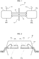
Figure 2 , anisolated system 20 may comprise afirst chip 2001 and asecond chip 2002 arranged on respective electrically isolateddie pads package 203. Each of thechips planar microantenna -
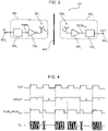
Figure 3 (also known from document Ragonese et al. cited previously) is a simplified circuit block diagram exemplary of an isolated data transfer channel of an isolated system (e.g., 10 or 20), andFigure 4 is exemplary of possible time behavior of electrical signals in the system. - Data transmission across a galvanic isolation barrier may rely on amplitude modulation of a radio-frequency (RF) carrier wave, in particular on on-off keying (OOK) pulse width modulation (PWM) of the RF carrier wave. A transmitting
chip 2001 comprises aninput pin 3001 for receiving an input digital signal IN carrying input data (e.g., a sequence of "0" or "1" bits), and a base-band interface 3021 (e.g., a PWM modulator circuit) which receives the input digital signal IN and produces a corresponding input PWM signal PWMIN for driving a transmission front-end circuit 3041. For instance, the signal PWMIN may comprise periods with a low duty-cycle (e.g., 25% or less) to encode a "0" bit value, and periods with a high duty-cycle (e.g., 75% or more) to encode a "1" bit value, as exemplified inFigure 4 . The transmission front-end circuit 3041 modulates the amplitude of a radio-frequency carrier wave as a function of the PWM signal PWMIN (e.g., applying ASK modulation, in particular OOK modulation) to produce the transmission signal SRF which is then transmitted by a transmittingantenna 2041 coupled to the transmission front-end circuit 3041. Thereceiving chip 2002, on the other side of theisolation barrier 306, comprises a reception front-end circuit 3042 coupled to the receivingantenna 2042 to receive the transmission signal SRF therefrom. The reception front-end circuit 3042 comprises an envelope detector circuit which detects the envelope of the transmission signal SRF to produce an output PWM signal PWMOUT. The output PWM signal PWMOUT is provided to a base-band interface 3022 for data demodulation (e.g., a PWM demodulator circuit), which produces an output digital signal OUT at anoutput pin 3002. - Therefore, the front-
end circuit 3042 in thereceiving chip 2002 is configured to rectify (e.g., perform envelope detection) and amplify the low-level radio-frequency signal SRF received so as to convert it into a PWM low frequency signal PWMOUT, thereby allowing inter-chip data communication with two micro-antennas which transmit and receive, respectively, a carrier signal. - Document Ragonese et al. cited previously provides an example of such a receiving front-end circuit, as exemplified in
Figures 5 and 6. Figure 5 is a simplified circuit block diagram exemplary of an isolated data transfer channel, andFigure 6 is a circuit block diagram exemplary of a portion of a corresponding receiving front-end circuit. - As exemplified in
Figure 5 , a receiving front-end circuit 3042 may comprise again stage 50, amixer stage 52 coupled to the output of thegain stage 50, and a low-pass filter stage 54 coupled to the output of themixer stage 52. The received radio-frequency signal SRF is first amplified at thegain stage 50 to obtain a signal having an amplitude suitable to drive the rectifier (e.g., amplifying the signal from about 80 mV amplitude to about 400 mV amplitude). Themixer stage 52 and the low-pass filter stage 54 (which together can be referred to as a rectifier stage in the context of the present description) then detect the envelope of the (amplified) input RF signal SRF and generate an envelope signal ENVOUT. The rectified (envelope) signal ENVOUT may be then compared to a threshold to generate the output PWM signal PWMOUT (the comparator circuit not being visible in the Figures annexed herein). -
Figure 6 is a circuit diagram exemplary of a rectifier stage as known from document Ragonese et al. cited previously: it consists of a differential amplifier with resistive load, with a double-balanced mixer based on a Gilbert cell. The output RC load of the mixer stage provides low-pass filtering to clean the RX signal envelope. Such a solution as disclosed by document Ragonese et al. cited previously is affected by a high current consumption due to both RF amplification and frequency limitations in the mixer-based rectifier. - Document Fiore V., Ragonese E., Palmisano G., "Low-Power ASK Detector for Low Modulation Indexes and Rail-to-Rail Input Range," in IEEE Transactions on Circuits and Systems II: Express Briefs, vol. 63, no. 5, pp. 458-462, May 2016, doi: 10.1109/TCSII.2015.2503651 (Fiore et al. hereinafter) discloses another example of an envelope detection circuit. However, that solution is not practical for use at low data rates, insofar as it cannot be fully integrated and needs external components.
- Therefore, there is a need in the art to provide an envelope detector circuit capable of converting a low-level radio-frequency carrier signal in a low frequency PWM signal, particularly for low data rate applications.
- An object of one or more embodiments is to contribute in providing such improved envelope detection circuits, e.g., for use in galvanic isolators, which can be fully integrated and operate at low data rates.
- According to one or more embodiments, such an object can be achieved by means of a circuit (e.g., an envelope detection circuit) having the features set forth in the claims that follow.
- One or more embodiments may relate to a corresponding receiver circuit.
- One or more embodiments may relate to a corresponding galvanic isolator device.
- The claims are an integral part of the technical teaching provided herein in respect of the embodiments.
- In one or more embodiments, a circuit may comprise a rectifier stage including a differential input transistor pair coupled between a reference voltage node and an intermediate node, and a load coupled between the intermediate node and a supply voltage node. The differential input transistor pair may be configured to receive a radio-frequency amplitude modulated signal. A rectified signal indicative of an envelope of the radio-frequency amplitude modulated signal may be produced at the intermediate node. The circuit may comprise an amplifier stage coupled to the intermediate node to receive the rectified signal, and configured to produce at an output node an amplified rectified signal indicative of the envelope of the radio-frequency amplitude modulated signal. The rectifier stage may comprise a first resistive element coupled between the intermediate node and the supply voltage node in parallel to the load.
- One or more embodiments may thus provide an envelope detector circuit which can operate at low data rates and can be fully integrated into a semiconductor chip.
- One or more embodiments will now be described, by way of example only, with reference to the annexed figures, wherein:
-
Figures 1 to 6 have already been discussed, -
Figure 7 is a circuit diagram exemplary of an envelope detector circuit, and -
Figure 8 is a circuit diagram exemplary of an envelope detector circuit according to one or more embodiments of the present description. - In the ensuing description, one or more specific details are illustrated, aimed at providing an in-depth understanding of examples of embodiments of this description. The embodiments may be obtained without one or more of the specific details, or with other methods, components, materials, etc. In other cases, known structures, materials, or operations are not illustrated or described in detail so that certain aspects of embodiments will not be obscured.
- Reference to "an embodiment" or "one embodiment" in the framework of the present description is intended to indicate that a particular configuration, structure, or characteristic described in relation to the embodiment is comprised in at least one embodiment. Hence, phrases such as "in an embodiment" or "in one embodiment" that may be present in one or more points of the present description do not necessarily refer to one and the same embodiment. Moreover, particular conformations, structures, or characteristics may be combined in any adequate way in one or more embodiments.
- The headings/references used herein are provided merely for convenience and hence do not define the extent of protection or the scope of the embodiments.
- Throughout the figures annexed herein, unless the context indicates otherwise, like parts or elements are indicated with like references/numerals and a corresponding description will not be repeated for brevity.
- By way of introduction to the detailed description of exemplary embodiments, reference may first be made to
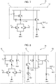
Figure 7 , which is a circuit diagram exemplary of a twostageenvelope detector circuit 70 suitable for use in an amplitude-shift keying (ASK) detector. - As exemplified in
Figure 7 , theenvelope detector circuit 70 may comprise aninput stage 71 and anoutput stage 72. - The
input stage 71 may comprise an input differential pair comprising two transistors (e.g., n-channel MOS transistors) M1 and M2. The input radio-frequency signal SRF may be applied between the (gate) control terminals of the two transistors M1 and M2 of the differential pair. The transistors M1, M2 may have their source terminals coupled to a reference voltage node GND and their drain terminals coupled to a commonintermediate node 710. - The
input stage 71 may comprise a load coupled between the commonintermediate node 710 and a supply node which provides a supply voltage VCC. For instance, as exemplified inFigure 7 , the load may comprise an active (e.g., self-biased) load including a transistor M3 and a low-pass filter RF, CF. The transistor M3 (e.g., a p-channel MOS transistor) may have its current path arranged between the commonintermediate node 710 and the supply node VCC. The low-pass filter may comprise a resistive element (e.g., a resistor RF) coupled between the commonintermediate node 710 and the (gate) control terminal of the transistor M3, and a capacitive element (e.g., a capacitor CF) coupled between the (gate) control terminal of the transistor M3 and the supply node VCC. - The
output stage 72 may comprise a common source or common emitter arrangement including a transistor M4 and a resistive load RL, the transistor M4 and the resistive load RL being coupled in series between the supply node Vcc and the reference voltage node GND. The transistor M4 may have a (gate) control terminal coupled to the common intermediate node 710 (acting as the output node of the first stage 71) . Anoutput node 720 intermediate the transistor M4 and the resistive load RL may provide the envelope output signal ENVOUT. In particular, the transistor M4 may be a p-channel MOS transistor having a source terminal coupled to the supply node VCC and a drain terminal coupled to theoutput node 720, and the resistive load RL may be coupled between the drain terminal of transistor M4 and the reference voltage node GND. - Therefore, in an
envelope detector circuit 70 as exemplified inFigure 7 , the (on-off) modulated differential input signal SRF is first rectified and then amplified to produce an envelope signal ENVOUT. Theoutput node 720 of theenvelope detector circuit 70 may be coupled to a comparator circuit (not visible in the Figures annexed herein) so that the envelope signal ENVOUT is converted into a single-ended rail-to-rail PWM data signal PWMOUT. - It is noted that a circuit as exemplified in
Figure 7 can be fully integrated in a silicon die (only) for use in high data rate communications. The small-signal loop gain T and the loop gain-bandwidth product fGBW can be computed according to the equations below:

- Assuming, by way of example, a high data rate equal to fBR = 100 Mb/s, then fGBW = fBR /25 = 4 MHz, and assuming also RF = 10 kΩ this leads to CF = 120 pF which is a high value, but still feasible to integrate into a silicon die.
- Assuming instead, again by way of example only, a low data rate equal to fBR = 400 kb/s, then fGBW = fBR /25 = 16 kHz, and assuming also RF = 75 kΩ this leads to CF = 4 nF which is a capacitance value too high to integrate into a silicon die.
- Therefore, at low data rates an envelope detector circuit as exemplified in
Figure 7 may require an external component (e.g., an external capacitor CF). - One or more embodiments may thus relate to an improved envelope detector circuit suitable for use (also) at low data rates, as exemplified in
Figure 8 , which is a circuit diagram exemplary of a three-stageenvelope detector circuit 80 suitable for use in an amplitude-shift keying (ASK) detector. - As exemplified in
Figure 8 , theenvelope detector circuit 80 may comprise aninput stage 81, anintermediate stage 82 and anoutput stage 83. - The
input stage 81 may comprise an input differential pair comprising two transistors (e.g., n-channel MOS transistors) M1 and M2. The input radio-frequency signal SRF may be applied between the (gate or base) control terminals of the two transistors M1 and M2 of the differential pair. The transistors M1, M2 may have their source or emitter terminals coupled to a reference voltage node GND and their drain or collector terminals coupled to a commonintermediate node 810. Theinput stage 81 may further comprise a load coupled between the commonintermediate node 810 and a supply node providing a supply voltage VCC. For instance, as exemplified inFigure 8 , the load may comprise an active (e.g., self-biased) load including a transistor M3 and a low-pass filter RF, CF. The transistor M3 (e.g., a p-channel MOS transistor) may have its current path arranged between the commonintermediate node 810 and the supply node VCC. The low-pass filter may comprise a resistive element (e.g., a resistor RF) coupled between the commonintermediate node 810 and the (gate or base) control terminal of the transistor M3, and a capacitive element (e.g., a capacitor CF) coupled between the (gate or base) control terminal of the transistor M3 and the supply node VCC . - As exemplified in
Figure 8 , theinput stage 81 may comprise a resistive element RL1 coupled in parallel to the active load, e.g., coupled between the commonintermediate node 810 and the supply node VCC. Arranging a further resistive element RL1 in theinput stage 81 provides a further degree of freedom in the design of theenvelope detector circuit 80, so that the resistive element RF can be set (e.g., dimensioned) to reduce the loop gain-bandwidth product fGBW , which in turn facilitates implementing the capacitive element CF as an integrated component, while RL1 can be set (e.g., dimensioned) so as to determine the gain and output pole frequency of theinput stage 81, thus mitigating (e.g., avoiding) edge distortions on the output PWM signal. - The
intermediate stage 82 may comprise a current matching circuit arrangement. As exemplified inFigure 8 , theintermediate stage 82 may comprise a transistor M4 (e.g., a p-channel MOS transistor) having a current path arranged between the supply node Vcc and abias source 822, and a control (gate or base) terminal coupled to theintermediate node 810 of theinput stage 81. A current I4 flows through the transistor M4. For instance, the transistor M4 may have a source or emitter terminal coupled to the supply node Vcc and a drain or collector terminal coupled to a furtherintermediate node 820, and thebias source 822 may comprise a current generator arranged between theintermediate node 820 and the reference voltage node GND to sink a bias current Ib from theintermediate node 820 towards the reference voltage node GND. - Additionally, the
intermediate stage 82 may comprise a resistive element RL2 coupled in parallel to the current path of transistor M4, e.g., coupled between theintermediate node 820 and the supply node VCC. Arranging a resistive element RL2 in theintermediate stage 82 facilitates restoring the matching conditions between the first stage 81 (transistor M3 and resistance RL1) and the second stage 82 (transistor M4 and resistance RL2), thus improving the accuracy in the bias current I5 of theoutput stage 83. - The
output stage 83 may comprise an amplifier stage, e.g., a folded amplifier stage. As exemplified inFigure 8 , theoutput stage 83 may comprise a current mirror arrangement comprising a first transistor M5 (e.g., a p-channel MOS transistor) and a second transistor M6 (e.g., a p-channel MOS transistor). The first transistor M5 may have a current path arranged between the supply node VCC and theintermediate node 820, through which a current I5 = Ib - I4 flows. The second transistor M6 may be arranged in series to an output load RL3 (e.g., a resistive load) between the supply node VCC and the reference voltage node GND, so that a copy of current I5 flows through M6 and RL3, thereby providing a single-ended output signal ENVOUT at thenode 830 intermediate the transistor M6 and the load RL3. - The folded amplifier comprising transistors M5 and M6 allows increasing the resistance value of the load RL3 and therefore the value of the second stage gain, insofar as the unipolar output signal ENVOUT becomes a positive voltage. Thus, the output bias voltage can be set to a value close to VCC. Purely by way of non-limiting example, with VCC = 3.5 V the resistance RL3 may be twice as big as the output load of a traditional configuration (e.g., RL in
Figure 7 ), thereby providing an additional gain of about 6 dB. - The
output node 830 of theenvelope detector circuit 80 may be coupled to a comparator circuit (not visible in the Figures annexed herein) so that the envelope signal ENVOUT is converted into a single-ended rail-to-rail PWM data signal PWMOUT. - It is noted that one or more embodiments as exemplified in
Figure 8 can be fully integrated in a silicon die (also) for use in low data rate communications. The small-signal loop gain T and the loop gain-bandwidth product fGBW can be computed according to the equations below:

- Assuming, by way of example, a low data rate equal to fBR = 400 kb/s, then fGBW = fBR /25 = 16 kHz, and assuming also RF = 2 MΩ and RL1 = 75 kΩ this leads to CF = 50 pF which is a capacitance value which can be integrated into a silicon die.
- One or more embodiments may be applied in a package-scale galvanic isolator device (e.g., as illustrated in
Figure 2 ), where galvanic isolation can be implemented without using specific high voltage components, the inter-chip communication channel can be implemented by means of a wireless radio-frequency transmission, and appropriately choosing the distance between the two chips facilitates achieving high isolation rating (e.g., 10 to 12 kV for reinforced isolation) and/or higher common mode transient immunity, CMTI (e.g., higher than 100 kV). - However, those of skill in the art will understand that reference to a package-scale galvanic isolator device is made by way of example only, and that one or more embodiments may be generally applied to any kind of galvanic isolator device.
- One or more embodiments have been disclosed herein with reference to specific implementations using complementary MOS technology. Those of skill in the art will understand that bipolar (BJT) technology can also be adopted as implementation technology for one or more embodiments, provided that it includes complementary transistors.
- One or more embodiments may thus provide an envelope detector circuit which can be fully integrated in a single chip (also) for use at low data rates, e.g., without using passive discrete components to operate the circuit at low data rates. By way of example, such envelope detector circuits may operate at frequencies lower than 1 MHz (e.g., in certain applications such as gate driver for motor control).
- One or more embodiments may additionally provide one or more of the following advantages: high immunity to common mode transients, low current consumption, high gain, and low cost.
- As exemplified herein, a circuit (e.g., 80) may comprise a rectifier stage (e.g., 81) including a differential input transistor pair (e.g., M1, M2) coupled between a reference voltage node (e.g., GND) and an intermediate node (e.g., 810), and a load (e.g., M3, RF, CF) coupled between the intermediate node and a supply voltage node (e.g., VCC ). The differential input transistor pair may be configured to receive a radio-frequency amplitude modulated signal (e.g., SRF+ , SRF- ). A rectified signal indicative of an envelope of the radio-frequency amplitude modulated signal may be produced at the intermediate node. The circuit may comprise an amplifier stage (e.g., 82; 83) coupled to the intermediate node to receive the rectified signal and configured to produce at an output node (e.g., 830) an amplified rectified signal (e.g., ENVOUT ) indicative of the envelope of the radio-frequency amplitude modulated signal. The rectifier stage may further comprise a first resistive element (e.g., RL1) coupled between the intermediate node and the supply voltage node in parallel to the load.
- As exemplified herein, the load may comprise an active load including a load transistor (e.g., M3) and a low-pass circuit arrangement (e.g., RF, CF).
- As exemplified herein, the active load may comprise the load transistor having a current path coupled between the intermediate node and the supply voltage node, a second resistive element (e.g., RF) coupled between the intermediate node and a control terminal of the load transistor, and a capacitive element (e.g., CF) coupled between the control terminal of the load transistor and the supply voltage node.
- As exemplified herein, the first resistive element may have a resistance value in the range of 25 kΩ to 50 kΩ, and the second resistive element may have a resistance value in the range of 1 MΩ to 3 MΩ. For instance, the first resistive element may be sized to correctly polarize the transistors M1, M2 and together with the biasing current (e.g., 2*Id1,2 where Id is the current flowing through one of the transistors M1, M2) it may define the gain of the first stage. For instance, an amplitude gain in the range of 2 to 3 may be obtained.
- As exemplified herein, the capacitive element may have a capacitance value in the range of 50 pF to 150 pF.
- As exemplified herein, the differential input transistor pair may comprise a first input transistor (e.g., M1) and a second input transistor (e.g., M2) having the current paths therethrough arranged in parallel between the reference voltage node and the intermediate node, and the control terminals of the first input transistor and the second input transistor may be configured to receive the radio-frequency amplitude modulated signal therebetween.
- As exemplified herein, the amplifier stage may comprise an output transistor (e.g., M6) arranged in a common source or common emitter configuration and an output load (e.g., RL3) coupled between a drain or collector terminal of the output transistor and the reference voltage node, and the output node may be intermediate the drain or collector terminal of the output transistor and the output load.
- As exemplified herein, the amplifier stage may comprise:
- a current-matching transistor (e.g., M4) having a current path arranged between the supply voltage node and a current control node (e.g., 820), and a control terminal coupled to the intermediate node;
- a bias source (e.g., 822) coupled between the current control node and the reference voltage node to sink a current (e.g., Ib ) from the current control node, and
- a current-mirroring transistor (e.g., M5) having a current path arranged between the supply voltage node and the current control node), and having a drain or collector terminal coupled to its control terminal.
- As exemplified herein, the control terminal of the current-mirroring transistor may be coupled to a control terminal of the output transistor.
- As exemplified herein, the circuit may comprise a current-matching resistive element (e.g., RL2) coupled between the supply voltage node and the current control node.
- As exemplified herein, the current-matching resistive element may have a resistance value in the range of 25 kΩ to 50 kΩ. For instance, the current-matching resistive element may be sized to correctly polarize the transistor M4 and together with the biasing current Ib it may define the gain of the second stage.
- As exemplified herein, the circuit may comprise a comparator circuit configured to compare the amplified rectified signal to a threshold signal to generate a pulse-width modulated output signal (e.g., PWMOUT ) indicative of the envelope of the radio-frequency amplitude modulated signal.
- As exemplified herein, a receiver circuit (e.g., 2002) may comprise:
- a radio-frequency antenna (e.g., 2042) configured to receive a radio-frequency amplitude modulated signal (e.g., SRF ),
- an envelope detector circuit according to one or more embodiments configured to receive the radio-frequency amplitude modulated signal from the antenna and to generate the pulse-width modulated output signal indicative of the envelope of the radio-frequency amplitude modulated signal received, and
- a PWM demodulator circuit (e.g., 3022) configured to demodulate the pulse-width modulated output signal to generate an output digital data signal (e.g., OUT).
- As exemplified herein, an isolator device (e.g., 20) may comprise a transmitter circuit (e.g., 2001) configured to transmit a radio-frequency amplitude modulated signal, and a receiver circuit according to one or more embodiments, and the transmitter circuit and the receiver circuit may be isolated by a galvanic isolation barrier (e.g., 306).
- As exemplified herein, the transmitter circuit and the receiver circuit may be provided as separate chips arranged on respective electrically-isolated die pads (e.g., 2021, 2022), and the isolator device may further comprise a molded package (e.g., 203) providing the galvanic isolation barrier.
- Without prejudice to the underlying principles, the details and embodiments may vary, even significantly, with respect to what has been described by way of example only, without departing from the extent of protection.
- The extent of protection is determined by the annexed claims.
Claims (13)
- A circuit (80), comprising:a rectifier stage (81) including a differential input transistor pair (M1, M2) coupled between a reference voltage node (GND) and an intermediate node (810), and a load (M3, RF, CF) coupled between the intermediate node (810) and a supply voltage node (VCC ), the differential input transistor pair (M1, M2) being configured to receive a radio-frequency amplitude modulated signal (SRF+ , SRF- ), wherein a rectified signal indicative of an envelope of said radio-frequency amplitude modulated signal (SRF+ , SRF- ) is produced at said intermediate node (810);an amplifier stage (82; 83) coupled to said intermediate node (810) to receive said rectified signal and configured to produce at an output node (830) an amplified rectified signal (ENVOUT ) indicative of the envelope of said radio-frequency amplitude modulated signal (SRF+, SRF- ),wherein the rectifier stage (81) further comprises a first resistive element (RL1) coupled between said intermediate node (810) and said supply voltage node (VCC ) in parallel to said load (M3, RF, CF).
- The circuit (80) of claim 1, wherein said load (M3, RF, CF) comprises an active load including a load transistor (M3) and a low-pass circuit arrangement (RF, CF).
- The circuit (80) of claim 2, wherein said active load comprises: said load transistor (M3) having a current path coupled between said intermediate node (810) and said supply voltage node (VCC ), a second resistive element (RF) coupled between said intermediate node (810) and a control terminal of said load transistor (M3), and a capacitive element (CF) coupled between said control terminal of said load transistor (M3) and said supply voltage node (VCC ).
- The circuit of claim 3, wherein said first resistive element (RL1) has a resistance value in the range of 25 kΩ to 50 kΩ, and said second resistive element (RF) has a resistance value in the range of 1 MΩ to 3 MΩ.
- The circuit (80) of any of the previous claims, wherein said differential input transistor pair (M1, M2) comprises a first input transistor (M1) and a second input transistor (M2) having the current paths therethrough arranged in parallel between said reference voltage node (GND) and said intermediate node (810), and wherein the control terminals of said first input transistor (M1) and said second input transistor (M2) are configured to receive said radio-frequency amplitude modulated signal (SRF+ , SRF- ) therebetween.
- The circuit (80) of any of the previous claims, wherein said amplifier stage (82; 83) comprises an output transistor (M6) arranged in a common source or common emitter configuration and an output load (RL3) coupled between a drain or collector terminal of said output transistor (M6) and said reference voltage node (GND), and wherein said output node (830) is intermediate said drain or collector terminal of said output transistor (M6) and said output load (RL3).
- The circuit (80) of claim 6, wherein said amplifier stage (82; 83) comprises:a current-matching transistor (M4) having a current path arranged between said supply voltage node (Vcc) and a current control node (820), and a control terminal coupled to said intermediate node (810);a bias source (822) coupled between said current control node (820) and said reference voltage node (GND) to sink a current (Ib ) from said current control node (820), anda current-mirroring transistor (M5) having a current path arranged between said supply voltage node (VCC ) and said current control node (820), and having a drain or collector terminal coupled to its control terminal,wherein the control terminal of said current-mirroring transistor (M5) is coupled to a control terminal of said output transistor (M6).
- The circuit (80) of claim 7, comprising a current-matching resistive element (RL2) coupled between said supply voltage node (VCC ) and said current control node (820).
- The circuit (80) of claim 8, wherein said current-matching resistive element (RL2) has a resistance value in the range of 25 kΩ to 50 kΩ.
- The circuit (80) of any of the previous claims, comprising a comparator circuit configured to compare said amplified rectified signal (ENVOUT ) to a threshold signal to generate a pulse-width modulated output signal (PWMOUT ) indicative of the envelope of said radio-frequency amplitude modulated signal (SRF+ , SRF- ).
- A receiver circuit (2002) comprising:a radio-frequency antenna (2042) configured to receive a radio-frequency amplitude modulated signal (SRF ),a circuit according to claim 10 configured to receive said radio-frequency amplitude modulated signal (SRF ) from said antenna and to generate said pulse-width modulated output signal (PWMOUT ) indicative of the envelope of said radio-frequency amplitude modulated signal (SRF ) received, anda PWM demodulator circuit (3022) configured to demodulate said pulse-width modulated output signal (PWMOUT ) to generate an output digital data signal (OUT) .
- An isolator device (20) comprising:a transmitter circuit (2001) configured to transmit a radio-frequency amplitude modulated signal (SRF ), anda receiver circuit (2002) according to claim 11,wherein the transmitter circuit (2001) and the receiver circuit (2002) are isolated by a galvanic isolation barrier (306).
- The isolator device (20) of claim 12, wherein the transmitter circuit (2001) and the receiver circuit (2002) are provided as separate chips arranged on respective electrically-isolated die pads (2021, 2022), the isolator device (20) further comprising a molded package (203) providing said galvanic isolation barrier.
Applications Claiming Priority (1)
| Application Number | Priority Date | Filing Date | Title |
|---|---|---|---|
| IT102021000007844A IT202100007844A1 (en) | 2021-03-30 | 2021-03-30 | MATCHING ENVELOPE DETECTOR CIRCUIT, RECEIVER CIRCUIT AND GALVANIC ISOLATOR DEVICE |
Publications (2)
| Publication Number | Publication Date |
|---|---|
| EP4068712A1 true EP4068712A1 (en) | 2022-10-05 |
| EP4068712B1 EP4068712B1 (en) | 2025-01-01 |
Family
ID=76270005
Family Applications (1)
| Application Number | Title | Priority Date | Filing Date |
|---|---|---|---|
| EP22164899.1A Active EP4068712B1 (en) | 2021-03-30 | 2022-03-29 | Envelope detector circuit, corresponding receiver circuit and galvanic isolator device |
Country Status (3)
| Country | Link |
|---|---|
| US (1) | US12095423B2 (en) |
| EP (1) | EP4068712B1 (en) |
| IT (1) | IT202100007844A1 (en) |
Families Citing this family (3)
| Publication number | Priority date | Publication date | Assignee | Title |
|---|---|---|---|---|
| US11621364B2 (en) * | 2020-07-22 | 2023-04-04 | Mpics Innovations Pte. Ltd | Isolation device and method of transmitting a signal across an isolation material using wire bonds |
| US12562727B2 (en) * | 2024-03-20 | 2026-02-24 | GM Global Technology Operations LLC | Variable slew-rate current source gate drivers for hybrid power modules |
| CN118555373B (en) * | 2024-07-29 | 2024-10-18 | 广东柔乐电器有限公司 | Two-wire low-power consumption visual intercom access control system |
Citations (1)
| Publication number | Priority date | Publication date | Assignee | Title |
|---|---|---|---|---|
| US8364195B2 (en) | 2007-05-11 | 2013-01-29 | Stmicroelectronics S.R.L. | Integrated galvanic isolator using wireless transmission |
Family Cites Families (17)
| Publication number | Priority date | Publication date | Assignee | Title |
|---|---|---|---|---|
| US7302055B1 (en) * | 2000-03-01 | 2007-11-27 | Intel Corporation | Discharging envelope detector |
| US6980006B1 (en) * | 2001-01-22 | 2005-12-27 | Cadence Design Systems, Inc. | High speed envelope detector and method |
| US7157944B1 (en) * | 2004-04-27 | 2007-01-02 | Altera Corporation | Differential signal detector methods and apparatus |
| US7269395B2 (en) * | 2004-08-04 | 2007-09-11 | Agency For Science, Technology And Research | Envelope detection circuit for low power communication systems |
| US7592869B2 (en) * | 2007-09-17 | 2009-09-22 | Finisar Corporation | Variable gain amplifier having dual gain control |
| US8254595B2 (en) * | 2008-03-25 | 2012-08-28 | Qualcomm Incorporated | System and method of companding an input signal of an energy detecting receiver |
| JP5165050B2 (en) * | 2008-04-08 | 2013-03-21 | 三菱電機株式会社 | High frequency amplifier |
| US9625498B2 (en) * | 2010-09-17 | 2017-04-18 | Hittite Microwave Llc | RMS and envelope detector |
| US9178476B2 (en) * | 2012-09-26 | 2015-11-03 | Broadcom Corporation | Envelope detector with enhanced linear range |
| US8841968B2 (en) * | 2012-09-26 | 2014-09-23 | Broadcom Corporation | Class-AB radio frequency amplifier for envelope detector |
| US9559646B2 (en) * | 2014-09-10 | 2017-01-31 | Samsung Electronics Co., Ltd | Apparatus and method for dynamically biased baseband current amplifier |
| CN105577580B (en) * | 2014-10-09 | 2019-01-08 | 扬智科技股份有限公司 | Envelope detection apparatus and related communication apparatus |
| US9819313B2 (en) * | 2016-01-26 | 2017-11-14 | Analog Devices, Inc. | Envelope detectors with high input impedance |
| US10627430B2 (en) * | 2016-05-24 | 2020-04-21 | Texas Instruments Incorporated | Fast current-based envelope detector |
| US10848109B2 (en) * | 2017-01-26 | 2020-11-24 | Analog Devices, Inc. | Bias modulation active linearization for broadband amplifiers |
| KR102454811B1 (en) * | 2017-07-18 | 2022-10-13 | 삼성전기주식회사 | Envelope-tracking current bias circuit with improved offset cancellation |
| US10804946B2 (en) * | 2017-11-17 | 2020-10-13 | The Regents Of The University Of California | Low power wake-up receiver |
-
2021
- 2021-03-30 IT IT102021000007844A patent/IT202100007844A1/en unknown
-
2022
- 2022-03-25 US US17/704,919 patent/US12095423B2/en active Active
- 2022-03-29 EP EP22164899.1A patent/EP4068712B1/en active Active
Patent Citations (1)
| Publication number | Priority date | Publication date | Assignee | Title |
|---|---|---|---|---|
| US8364195B2 (en) | 2007-05-11 | 2013-01-29 | Stmicroelectronics S.R.L. | Integrated galvanic isolator using wireless transmission |
Non-Patent Citations (4)
| Title |
|---|
| FIORE V.RAGONESE E.PALMISANO G.: "Low-Power ASK Detector for Low Modulation Indexes and Rail-to-Rail Input Range", IEEE TRANSACTIONS ON CIRCUITS AND SYSTEMS II: EXPRESS BRIEFS, vol. 63, no. 5, May 2016 (2016-05-01), pages 458 - 462, XP011607869, DOI: 10.1109/TCSII.2015.2503651 |
| FIORE VINCENZO ET AL: "Low-Power ASK Detector for Low Modulation Indexes and Rail-to-Rail Input Range", IEEE TRANSACTIONS ON CIRCUITS AND SYSTEMS II: EXPRESS BRIEFS, IEEE, USA, vol. 63, no. 5, 1 May 2016 (2016-05-01), pages 458 - 462, XP011607869, ISSN: 1549-7747, [retrieved on 20160428], DOI: 10.1109/TCSII.2015.2503651 * |
| PIERPAOLO LOMBARDO ET AL: "ISSCC 2016 / SESSION 16 / INNOVATIONS IN CIRCUITS AND SYSTEMS ENABLED BY NOVEL TECHNOLOGIES / 16.7 16.7 A Fully-Integrated Half-Duplex Data/Power Transfer System with up to 40Mb/s Data Rate, 23mW Output Power and On-Chip 5kV Galvanic Isolation", 25 February 2016 (2016-02-25), XP055377488, Retrieved from the Internet <URL:http://ieeexplore.ieee.org/ielx7/7405163/7417881/07418026.pdf?tp=&arnumber=7418026&isnumber=7417881> [retrieved on 20170531] * |
| RAGONESE EGIDIO ET AL: "A Fully Integrated Galvanically Isolated DC-DC Converter With Data Communication", IEEE TRANSACTIONS ON CIRCUITS AND SYSTEMS I: REGULAR PAPERS, IEEE, US, vol. 65, no. 4, 1 April 2018 (2018-04-01), pages 1432 - 1441, XP011678911, ISSN: 1549-8328, [retrieved on 20180309], DOI: 10.1109/TCSI.2017.2742021 * |
Also Published As
| Publication number | Publication date |
|---|---|
| IT202100007844A1 (en) | 2022-09-30 |
| EP4068712B1 (en) | 2025-01-01 |
| US20220329207A1 (en) | 2022-10-13 |
| US12095423B2 (en) | 2024-09-17 |
Similar Documents
| Publication | Publication Date | Title |
|---|---|---|
| EP4068712B1 (en) | Envelope detector circuit, corresponding receiver circuit and galvanic isolator device | |
| US8903332B2 (en) | Circuit device and method of coupling to an antenna | |
| CN102832917B (en) | Switch driving circuit | |
| US12218645B2 (en) | Isolation communications channel using direct demodulation and data-edge encoding | |
| US20180062678A1 (en) | Galvanic isolation circuit, corresponding system and method | |
| US8975914B2 (en) | Isolation receiver | |
| CN101826646B (en) | Semiconductor switch, semiconductor switch MMIC, changeover switch RF module, power switch RF module, and transceiver module | |
| EP1766774A2 (en) | Power amplifier utilizing high breakdown voltage circuit topology | |
| US20250202089A1 (en) | Digital isolator | |
| KR0160574B1 (en) | Amplifier for use in a radio telephone | |
| CN117640308A (en) | Demodulation module, digital isolator, chip, demodulation method and electronic equipment | |
| US11621670B1 (en) | Capacitively-coupled stacked class-d oscillators for galvanic isolation | |
| CN115149907B (en) | Envelope detector circuit, corresponding receiver circuit and current isolator device | |
| US20230034417A1 (en) | Isolated communications lane demodulator | |
| US11418190B2 (en) | Switch circuits and transistor stacks with capacitor networks for balancing off-state RF voltages and methods of their operation | |
| US8135357B1 (en) | Integrated transmitter/receiver switch with impedance matching network | |
| EP4401323A1 (en) | Receiver circuit, corresponding system and method | |
| CN117278005A (en) | High-speed capacitive isolation OOK signal modulation and demodulation circuit | |
| US6710716B1 (en) | Power detecting circuit and demodulator comprising the same | |
| CN110995224A (en) | Switch structure with transceiving switching and polarization switching functions | |
| US11901863B2 (en) | Capacitively-coupled stacked class-D oscillators for galvanic isolation | |
| EP4350723A1 (en) | Semiconductor die with transformer and esd clamp circuit | |
| US12315979B2 (en) | Spread spectrum modulation technique for isolation devices | |
| CN114268287B (en) | One-way microwave limiter and communication system | |
| US20240333318A1 (en) | Communication circuit, corresponding system and method |
Legal Events
| Date | Code | Title | Description |
|---|---|---|---|
| PUAI | Public reference made under article 153(3) epc to a published international application that has entered the european phase |
Free format text: ORIGINAL CODE: 0009012 |
|
| STAA | Information on the status of an ep patent application or granted ep patent |
Free format text: STATUS: THE APPLICATION HAS BEEN PUBLISHED |
|
| AK | Designated contracting states |
Kind code of ref document: A1 Designated state(s): AL AT BE BG CH CY CZ DE DK EE ES FI FR GB GR HR HU IE IS IT LI LT LU LV MC MK MT NL NO PL PT RO RS SE SI SK SM TR |
|
| STAA | Information on the status of an ep patent application or granted ep patent |
Free format text: STATUS: REQUEST FOR EXAMINATION WAS MADE |
|
| 17P | Request for examination filed |
Effective date: 20230315 |
|
| RBV | Designated contracting states (corrected) |
Designated state(s): AL AT BE BG CH CY CZ DE DK EE ES FI FR GB GR HR HU IE IS IT LI LT LU LV MC MK MT NL NO PL PT RO RS SE SI SK SM TR |
|
| RIC1 | Information provided on ipc code assigned before grant |
Ipc: H04L 25/49 20060101ALI20240729BHEP Ipc: H04L 25/02 20060101AFI20240729BHEP |
|
| GRAP | Despatch of communication of intention to grant a patent |
Free format text: ORIGINAL CODE: EPIDOSNIGR1 |
|
| STAA | Information on the status of an ep patent application or granted ep patent |
Free format text: STATUS: GRANT OF PATENT IS INTENDED |
|
| INTG | Intention to grant announced |
Effective date: 20240930 |
|
| GRAS | Grant fee paid |
Free format text: ORIGINAL CODE: EPIDOSNIGR3 |
|
| GRAA | (expected) grant |
Free format text: ORIGINAL CODE: 0009210 |
|
| STAA | Information on the status of an ep patent application or granted ep patent |
Free format text: STATUS: THE PATENT HAS BEEN GRANTED |
|
| AK | Designated contracting states |
Kind code of ref document: B1 Designated state(s): AL AT BE BG CH CY CZ DE DK EE ES FI FR GB GR HR HU IE IS IT LI LT LU LV MC MK MT NL NO PL PT RO RS SE SI SK SM TR |
|
| REG | Reference to a national code |
Ref country code: GB Ref legal event code: FG4D |
|
| REG | Reference to a national code |
Ref country code: CH Ref legal event code: EP |
|
| REG | Reference to a national code |
Ref country code: DE Ref legal event code: R096 Ref document number: 602022009225 Country of ref document: DE |
|
| REG | Reference to a national code |
Ref country code: IE Ref legal event code: FG4D |
|
| PGFP | Annual fee paid to national office [announced via postgrant information from national office to epo] |
Ref country code: AT Payment date: 20250417 Year of fee payment: 4 |
|
| REG | Reference to a national code |
Ref country code: LT Ref legal event code: MG9D |
|
| REG | Reference to a national code |
Ref country code: NL Ref legal event code: MP Effective date: 20250101 |
|
| REG | Reference to a national code |
Ref country code: AT Ref legal event code: MK05 Ref document number: 1757439 Country of ref document: AT Kind code of ref document: T Effective date: 20250101 |
|
| PG25 | Lapsed in a contracting state [announced via postgrant information from national office to epo] |
Ref country code: NL Free format text: LAPSE BECAUSE OF FAILURE TO SUBMIT A TRANSLATION OF THE DESCRIPTION OR TO PAY THE FEE WITHIN THE PRESCRIBED TIME-LIMIT Effective date: 20250101 |
|
| PG25 | Lapsed in a contracting state [announced via postgrant information from national office to epo] |
Ref country code: FI Free format text: LAPSE BECAUSE OF FAILURE TO SUBMIT A TRANSLATION OF THE DESCRIPTION OR TO PAY THE FEE WITHIN THE PRESCRIBED TIME-LIMIT Effective date: 20250101 |
|
| PG25 | Lapsed in a contracting state [announced via postgrant information from national office to epo] |
Ref country code: PL Free format text: LAPSE BECAUSE OF FAILURE TO SUBMIT A TRANSLATION OF THE DESCRIPTION OR TO PAY THE FEE WITHIN THE PRESCRIBED TIME-LIMIT Effective date: 20250101 |
|
| PG25 | Lapsed in a contracting state [announced via postgrant information from national office to epo] |
Ref country code: ES Free format text: LAPSE BECAUSE OF FAILURE TO SUBMIT A TRANSLATION OF THE DESCRIPTION OR TO PAY THE FEE WITHIN THE PRESCRIBED TIME-LIMIT Effective date: 20250101 |
|
| PG25 | Lapsed in a contracting state [announced via postgrant information from national office to epo] |
Ref country code: NO Free format text: LAPSE BECAUSE OF FAILURE TO SUBMIT A TRANSLATION OF THE DESCRIPTION OR TO PAY THE FEE WITHIN THE PRESCRIBED TIME-LIMIT Effective date: 20250401 Ref country code: IS Free format text: LAPSE BECAUSE OF FAILURE TO SUBMIT A TRANSLATION OF THE DESCRIPTION OR TO PAY THE FEE WITHIN THE PRESCRIBED TIME-LIMIT Effective date: 20250501 |
|
| PG25 | Lapsed in a contracting state [announced via postgrant information from national office to epo] |
Ref country code: HR Free format text: LAPSE BECAUSE OF FAILURE TO SUBMIT A TRANSLATION OF THE DESCRIPTION OR TO PAY THE FEE WITHIN THE PRESCRIBED TIME-LIMIT Effective date: 20250101 |
|
| PG25 | Lapsed in a contracting state [announced via postgrant information from national office to epo] |
Ref country code: LV Free format text: LAPSE BECAUSE OF FAILURE TO SUBMIT A TRANSLATION OF THE DESCRIPTION OR TO PAY THE FEE WITHIN THE PRESCRIBED TIME-LIMIT Effective date: 20250101 Ref country code: PT Free format text: LAPSE BECAUSE OF FAILURE TO SUBMIT A TRANSLATION OF THE DESCRIPTION OR TO PAY THE FEE WITHIN THE PRESCRIBED TIME-LIMIT Effective date: 20250502 |
|
| PG25 | Lapsed in a contracting state [announced via postgrant information from national office to epo] |
Ref country code: GR Free format text: LAPSE BECAUSE OF FAILURE TO SUBMIT A TRANSLATION OF THE DESCRIPTION OR TO PAY THE FEE WITHIN THE PRESCRIBED TIME-LIMIT Effective date: 20250402 Ref country code: BG Free format text: LAPSE BECAUSE OF FAILURE TO SUBMIT A TRANSLATION OF THE DESCRIPTION OR TO PAY THE FEE WITHIN THE PRESCRIBED TIME-LIMIT Effective date: 20250101 |
|
| PG25 | Lapsed in a contracting state [announced via postgrant information from national office to epo] |
Ref country code: AT Free format text: LAPSE BECAUSE OF FAILURE TO SUBMIT A TRANSLATION OF THE DESCRIPTION OR TO PAY THE FEE WITHIN THE PRESCRIBED TIME-LIMIT Effective date: 20250101 |
|
| PG25 | Lapsed in a contracting state [announced via postgrant information from national office to epo] |
Ref country code: CZ Free format text: LAPSE BECAUSE OF FAILURE TO SUBMIT A TRANSLATION OF THE DESCRIPTION OR TO PAY THE FEE WITHIN THE PRESCRIBED TIME-LIMIT Effective date: 20250101 |
|
| PG25 | Lapsed in a contracting state [announced via postgrant information from national office to epo] |
Ref country code: SE Free format text: LAPSE BECAUSE OF FAILURE TO SUBMIT A TRANSLATION OF THE DESCRIPTION OR TO PAY THE FEE WITHIN THE PRESCRIBED TIME-LIMIT Effective date: 20250101 |
|
| REG | Reference to a national code |
Ref country code: DE Ref legal event code: R097 Ref document number: 602022009225 Country of ref document: DE |
|
| PG25 | Lapsed in a contracting state [announced via postgrant information from national office to epo] |
Ref country code: SM Free format text: LAPSE BECAUSE OF FAILURE TO SUBMIT A TRANSLATION OF THE DESCRIPTION OR TO PAY THE FEE WITHIN THE PRESCRIBED TIME-LIMIT Effective date: 20250101 |
|
| PG25 | Lapsed in a contracting state [announced via postgrant information from national office to epo] |
Ref country code: DK Free format text: LAPSE BECAUSE OF FAILURE TO SUBMIT A TRANSLATION OF THE DESCRIPTION OR TO PAY THE FEE WITHIN THE PRESCRIBED TIME-LIMIT Effective date: 20250101 |
|
| PG25 | Lapsed in a contracting state [announced via postgrant information from national office to epo] |
Ref country code: MC Free format text: LAPSE BECAUSE OF FAILURE TO SUBMIT A TRANSLATION OF THE DESCRIPTION OR TO PAY THE FEE WITHIN THE PRESCRIBED TIME-LIMIT Effective date: 20250101 |
|
| PG25 | Lapsed in a contracting state [announced via postgrant information from national office to epo] |
Ref country code: IT Free format text: LAPSE BECAUSE OF FAILURE TO SUBMIT A TRANSLATION OF THE DESCRIPTION OR TO PAY THE FEE WITHIN THE PRESCRIBED TIME-LIMIT Effective date: 20250101 |
|
| PG25 | Lapsed in a contracting state [announced via postgrant information from national office to epo] |
Ref country code: EE Free format text: LAPSE BECAUSE OF FAILURE TO SUBMIT A TRANSLATION OF THE DESCRIPTION OR TO PAY THE FEE WITHIN THE PRESCRIBED TIME-LIMIT Effective date: 20250101 |
|
| REG | Reference to a national code |
Ref country code: CH Ref legal event code: H13 Free format text: ST27 STATUS EVENT CODE: U-0-0-H10-H13 (AS PROVIDED BY THE NATIONAL OFFICE) Effective date: 20251023 |
|
| PG25 | Lapsed in a contracting state [announced via postgrant information from national office to epo] |
Ref country code: RO Free format text: LAPSE BECAUSE OF FAILURE TO SUBMIT A TRANSLATION OF THE DESCRIPTION OR TO PAY THE FEE WITHIN THE PRESCRIBED TIME-LIMIT Effective date: 20250101 |
|
| PG25 | Lapsed in a contracting state [announced via postgrant information from national office to epo] |
Ref country code: SK Free format text: LAPSE BECAUSE OF FAILURE TO SUBMIT A TRANSLATION OF THE DESCRIPTION OR TO PAY THE FEE WITHIN THE PRESCRIBED TIME-LIMIT Effective date: 20250101 |
|
| PLBE | No opposition filed within time limit |
Free format text: ORIGINAL CODE: 0009261 |
|
| STAA | Information on the status of an ep patent application or granted ep patent |
Free format text: STATUS: NO OPPOSITION FILED WITHIN TIME LIMIT |
|
| PG25 | Lapsed in a contracting state [announced via postgrant information from national office to epo] |
Ref country code: LU Free format text: LAPSE BECAUSE OF NON-PAYMENT OF DUE FEES Effective date: 20250329 |
|
| 26N | No opposition filed |
Effective date: 20251002 |
|
| REG | Reference to a national code |
Ref country code: BE Ref legal event code: MM Effective date: 20250331 |
|
| PG25 | Lapsed in a contracting state [announced via postgrant information from national office to epo] |
Ref country code: FR Free format text: LAPSE BECAUSE OF NON-PAYMENT OF DUE FEES Effective date: 20250331 |
|
| PG25 | Lapsed in a contracting state [announced via postgrant information from national office to epo] |
Ref country code: BE Free format text: LAPSE BECAUSE OF NON-PAYMENT OF DUE FEES Effective date: 20250331 |
|
| PG25 | Lapsed in a contracting state [announced via postgrant information from national office to epo] |
Ref country code: CH Free format text: LAPSE BECAUSE OF NON-PAYMENT OF DUE FEES Effective date: 20250331 |
|
| PG25 | Lapsed in a contracting state [announced via postgrant information from national office to epo] |
Ref country code: IE Free format text: LAPSE BECAUSE OF NON-PAYMENT OF DUE FEES Effective date: 20250329 |
|
| PGFP | Annual fee paid to national office [announced via postgrant information from national office to epo] |
Ref country code: DE Payment date: 20260219 Year of fee payment: 5 |