EP4068625A1 - Joined body of piezoelectric material substrate and support substrate - Google Patents
Joined body of piezoelectric material substrate and support substrate Download PDFInfo
- Publication number
- EP4068625A1 EP4068625A1 EP20893072.7A EP20893072A EP4068625A1 EP 4068625 A1 EP4068625 A1 EP 4068625A1 EP 20893072 A EP20893072 A EP 20893072A EP 4068625 A1 EP4068625 A1 EP 4068625A1
- Authority
- EP
- European Patent Office
- Prior art keywords
- piezoelectric material
- bonding
- substrate
- material substrate
- bonding surface
- Prior art date
- Legal status (The legal status is an assumption and is not a legal conclusion. Google has not performed a legal analysis and makes no representation as to the accuracy of the status listed.)
- Granted
Links
Images



Classifications
-
- H—ELECTRICITY
- H03—ELECTRONIC CIRCUITRY
- H03H—IMPEDANCE NETWORKS, e.g. RESONANT CIRCUITS; RESONATORS
- H03H9/00—Networks comprising electromechanical or electro-acoustic elements; Electromechanical resonators
- H03H9/02—Details
- H03H9/02535—Details of surface acoustic wave devices
- H03H9/02543—Characteristics of substrate, e.g. cutting angles
- H03H9/02574—Characteristics of substrate, e.g. cutting angles of combined substrates, multilayered substrates, piezoelectrical layers on not-piezoelectrical substrate
-
- H—ELECTRICITY
- H03—ELECTRONIC CIRCUITRY
- H03H—IMPEDANCE NETWORKS, e.g. RESONANT CIRCUITS; RESONATORS
- H03H9/00—Networks comprising electromechanical or electro-acoustic elements; Electromechanical resonators
- H03H9/02—Details
- H03H9/02535—Details of surface acoustic wave devices
- H03H9/02543—Characteristics of substrate, e.g. cutting angles
- H03H9/02559—Characteristics of substrate, e.g. cutting angles of lithium niobate or lithium-tantalate substrates
-
- G—PHYSICS
- G01—MEASURING; TESTING
- G01B—MEASURING LENGTH, THICKNESS OR SIMILAR LINEAR DIMENSIONS; MEASURING ANGLES; MEASURING AREAS; MEASURING IRREGULARITIES OF SURFACES OR CONTOURS
- G01B15/00—Measuring arrangements characterised by the use of electromagnetic waves or particle radiation, e.g. by the use of microwaves, X-rays, gamma rays or electrons
- G01B15/08—Measuring arrangements characterised by the use of electromagnetic waves or particle radiation, e.g. by the use of microwaves, X-rays, gamma rays or electrons for measuring roughness or irregularity of surfaces
-
- H—ELECTRICITY
- H03—ELECTRONIC CIRCUITRY
- H03H—IMPEDANCE NETWORKS, e.g. RESONANT CIRCUITS; RESONATORS
- H03H3/00—Apparatus or processes specially adapted for the manufacture of impedance networks, resonating circuits, resonators
- H03H3/007—Apparatus or processes specially adapted for the manufacture of impedance networks, resonating circuits, resonators for the manufacture of electromechanical resonators or networks
- H03H3/08—Apparatus or processes specially adapted for the manufacture of impedance networks, resonating circuits, resonators for the manufacture of electromechanical resonators or networks for the manufacture of resonators or networks using surface acoustic waves
-
- H—ELECTRICITY
- H03—ELECTRONIC CIRCUITRY
- H03H—IMPEDANCE NETWORKS, e.g. RESONANT CIRCUITS; RESONATORS
- H03H9/00—Networks comprising electromechanical or electro-acoustic elements; Electromechanical resonators
- H03H9/02—Details
- H03H9/02535—Details of surface acoustic wave devices
- H03H9/02818—Means for compensation or elimination of undesirable effects
- H03H9/02834—Means for compensation or elimination of undesirable effects of temperature influence
-
- H—ELECTRICITY
- H03—ELECTRONIC CIRCUITRY
- H03H—IMPEDANCE NETWORKS, e.g. RESONANT CIRCUITS; RESONATORS
- H03H9/00—Networks comprising electromechanical or electro-acoustic elements; Electromechanical resonators
- H03H9/25—Constructional features of resonators using surface acoustic waves
-
- H—ELECTRICITY
- H10—SEMICONDUCTOR DEVICES; ELECTRIC SOLID-STATE DEVICES NOT OTHERWISE PROVIDED FOR
- H10N—ELECTRIC SOLID-STATE DEVICES NOT OTHERWISE PROVIDED FOR
- H10N30/00—Piezoelectric or electrostrictive devices
- H10N30/01—Manufacture or treatment
- H10N30/07—Forming of piezoelectric or electrostrictive parts or bodies on an electrical element or another base
- H10N30/072—Forming of piezoelectric or electrostrictive parts or bodies on an electrical element or another base by laminating or bonding of piezoelectric or electrostrictive bodies
-
- H—ELECTRICITY
- H10—SEMICONDUCTOR DEVICES; ELECTRIC SOLID-STATE DEVICES NOT OTHERWISE PROVIDED FOR
- H10N—ELECTRIC SOLID-STATE DEVICES NOT OTHERWISE PROVIDED FOR
- H10N30/00—Piezoelectric or electrostrictive devices
- H10N30/01—Manufacture or treatment
- H10N30/07—Forming of piezoelectric or electrostrictive parts or bodies on an electrical element or another base
- H10N30/072—Forming of piezoelectric or electrostrictive parts or bodies on an electrical element or another base by laminating or bonding of piezoelectric or electrostrictive bodies
- H10N30/073—Forming of piezoelectric or electrostrictive parts or bodies on an electrical element or another base by laminating or bonding of piezoelectric or electrostrictive bodies by fusion of metals or by adhesives
-
- H—ELECTRICITY
- H10—SEMICONDUCTOR DEVICES; ELECTRIC SOLID-STATE DEVICES NOT OTHERWISE PROVIDED FOR
- H10P—GENERIC PROCESSES OR APPARATUS FOR THE MANUFACTURE OR TREATMENT OF DEVICES COVERED BY CLASS H10
- H10P10/00—Bonding of wafers, substrates or parts of devices
- H10P10/12—Bonding of semiconductor wafers or semiconductor substrates to semiconductor wafers or semiconductor substrates
- H10P10/126—Bonding of semiconductor wafers or semiconductor substrates to semiconductor wafers or semiconductor substrates characterised by the composition of the bonding layer, e.g. dopant concentration or stoichiometry
-
- H—ELECTRICITY
- H10—SEMICONDUCTOR DEVICES; ELECTRIC SOLID-STATE DEVICES NOT OTHERWISE PROVIDED FOR
- H10P—GENERIC PROCESSES OR APPARATUS FOR THE MANUFACTURE OR TREATMENT OF DEVICES COVERED BY CLASS H10
- H10P90/00—Preparation of wafers not covered by a single main group of this subclass, e.g. wafer reinforcement
- H10P90/19—Preparing inhomogeneous wafers
- H10P90/1904—Preparing vertically inhomogeneous wafers
- H10P90/1906—Preparing SOI wafers
- H10P90/1922—Preparing SOI wafers using silicon etch back techniques, e.g. BESOI or ELTRAN
-
- H—ELECTRICITY
- H10—SEMICONDUCTOR DEVICES; ELECTRIC SOLID-STATE DEVICES NOT OTHERWISE PROVIDED FOR
- H10W—GENERIC PACKAGES, INTERCONNECTIONS, CONNECTORS OR OTHER CONSTRUCTIONAL DETAILS OF DEVICES COVERED BY CLASS H10
- H10W10/00—Isolation regions in semiconductor bodies between components of integrated devices
- H10W10/10—Isolation regions comprising dielectric materials
- H10W10/181—Semiconductor-on-insulator [SOI] isolation regions, e.g. buried oxide regions of SOI wafers
Definitions
- the present invention relates to a bonded body of a piezoelectric material substrate and supporting substrate and an acoustic wave device.
- the bonding surface is made a roughened surface
- the ratio of an average length RSm of a factor in a cross sectional profile of convex-concave structure forming the roughened surface and a wavelength ⁇ of a surface acoustic wave is made 0.2 or larger and 7.0 or smaller and the arithmetic average roughness Ra of the cross sectional profile of the convex-concave structure is made 100nm or larger. Further, it is defined a difference in height of a roughened surface in the patent document 2.
- An object of the present invention is to provide a novel structure for suppressing the spurious wave which cannot be suppressed by adjusting the surface morphology of a bonding surface of a piezoelectric material substrate or supporting substrate of a bonded body.
- the present invention provides a bonded body comprising:
- the inventors have tried to make the bonding surface of the supporting substrate or piezoelectric material substrate a mirror surface and then to form a roughened surface by mechanical processing, and the microstructure was observed and analyzed in detail. As a result, it is found that minute defects or denaturing of the film, which cannot be evaluated based on the surface convex-concave morphology, are generated on the bonding surface after the mechanical processing. Based on such measurement results, it is found that the effect of suppressing the spurious wave is needed to be controlled based not on the surface convex-concave morphology and based on the effective crystallographic and geometric characteristics in surface regions of the piezoelectric material substrate and bonding layer.
- the present inventors have researched various kinds of processing and measuring methods of the bonding surface. During the research, the inventors noticed X-ray reflectivity method (XRR method, X-ray Reflection).
- XRR method X-ray Reflectivity method
- the X-ray reflectivity method X-ray is made incident onto a surface of a sample at an extremely low angle, and it is measured the X-ray intensity profile of reflected light reflected in the mirror direction of the incident angle.
- the profile obtained by the measurement is compared with the simulation results and the simulation parameters are optimized so that the film thickness and density of the sample are determined.
- the X-ray reflectivity method is originally the method of measuring the film thickness and density of a thin film utilizing X-ray reflection from the thin film. It means that the reflected light reflected from the thin film carries information of the convex-concave of the surface of the thin film as well as information in the direction of depth of the thin film (film thickness and density).
- the inventors tried to apply the X-ray reflectivity method onto the bonding surface after the roughening process of the piezoelectric material substrate or supporting substrate and to obtain information of denaturing or change of density in a region near the surface of the bonding surface, and researched the relationship of the information and the effect of suppressing the spurious wave.
- the bonding surface of the piezoelectric material substrate or supporting substrate is subjected to roughening process. Thereafter, the information of crystallographic state in the surface region of the bonding surface is obtained by the X-ray reflectivity method. Specifically, X-ray is made incident onto the bonding surface at a very low angle and the reflected light is then measured.
- ⁇ is assigned to the incident angle of the X-ray, and ⁇ is gradually changed from 0 ° to record the relative intensity I of the reflected light.
- the relative intensity I is defined as a relative intensity provided that 1 is assigned to the signal intensity at the total reflection. It is known that the relative intensity I is damped in proportion with 1 ⁇ 10 -4 in the case that the bonding surface is ideally flat.
- the inventors performed the measurement of the bonding surface after various kinds of roughening processes by the X-ray reflectivity method, respectively, and measured the degree of suppressing the spurious wave. As a result, it is found that the relative density I of the reflected light from the bonding surface can be approximated with the formula (1), in a range of 1.0 ⁇ 10 -4 or larger and 1.0 ⁇ 10 -1 or smaller.
- the index b is 5.0 or larger and coefficient a can be approximated as 1.0 ⁇ 10 -5 to 2.0 ⁇ 10 -3 . It means that the relative intensity I is decreased more rapidly as the increase of the incident angle ⁇ than the case that the bonding surface is a mirror surface. Further, it means that the crystals are denatured in the surface region of the bonding surface or defects are generated other than the minute convex-concave morphology on the surface. It is found that the spurious wave can be suppressed under such condition.
- a supporting substrate 1 having a pair of main surfaces 1a and 1b.
- Processing A is then performed on the main surface (bonding surface) 1a to roughen the surface.
- a bonding layer 2 is film-formed on the main surface 1a of the supporting substrate 1.
- the surface 2a of the bonding layer 2 is subjected to CMP polishing for obtaining a mirror surface.
- plasma is irradiated onto the surface 2a of the bonding layer 2 to obtain a surface-activated bonding surface 2b.
- a piezoelectric material substrate 3 having a main surface 3a.
- Plasma is then irradiated onto the main surface of the piezoelectric material substrate 3 as arrows C to activate the surface to form a surface-activated bonding surface 3b.
- the activated bonding surface 2b of the bonding layer 2 on the supporting substrate and the activated bonding surface 3b of the piezoelectric material substrate 3 are contacted with each other and subjected to direct bonding, to obtain a bonded body 5 shown in Fig. 4(a) .
- electrodes may be provided on the piezoelectric material substrate 3.
- the main surface 3c of the piezoelectric material substrate 3 is processed to thin the substrate 3A to form a thinned piezoelectric material substrate 3A so that a bonded body 5A is provided.
- 9 represents a processed surface.
- predetermined electrodes 10 may be formed on the processed surface 9 of the piezoelectric material substrate 3A of the bonded body 5A to obtain an acoustic wave device 6.
- Figs. 5 and 6 relate to this embodiment.
- a supporting substrate 1 having a pair of main surfaces 1a and 1b.
- Processing A is then performed on the main surface (bonding surface) 1a for the roughening.
- a bonding layer 2 is film-formed on the main surface 1a of the supporting substrate 1.
- the surface of the bonding layer 2 is subjected to CMP polishing for obtaining a mirror surface.
- plasma is irradiated onto the bonding surface of the bonding layer 2 as arrows B to obtain a surface-activated bonding surface 2b.
- a piezoelectric material substrate 3 having a main surface 3a.
- an intermediate layer 12 is formed on the main surface (bonding surface) 3a of the piezoelectric material substrate 3, and plasma is irradiated onto the surface of the intermediate layer 12 as arrows C to perform the surface activation to form a surface-activated bonding surface 12a.
- the activated surface 2b of the bonding layer 2 on the supporting substrate and the activated bonding surface 12a of the intermediate layer 12 on the piezoelectric material substrate 3 are contacted with and directly bonded with each other, to obtain a bonded body 15 shown in Fig. 6(a) .
- electrodes may be provided on the piezoelectric material substrate 3.
- the main surface 3c of the piezoelectric material substrate 3 is processed to thin the substrate 3 to form a thinned piezoelectric material substrate 3A so that a bonded body 15A is provided.
- 9 represents a processed surface.
- predetermined electrodes 10 may be formed on the processed surface 9 of the piezoelectric material substrate 3A of the bonded body 15A to obtain an acoustic wave device 16.
- the intermediate layer 12 may be subsequently film-formed on the bonding layer 2.
- CMP processing is performed on the surface of the intermediate layer 12 to obtain a bonding surface (mirror surface). Plasma is irradiated onto the thus obtained bonding surface to activate the surface. The surface of the supporting substrate is then subjected to plasma activation and directly bonded with the bonding surface of the intermediate layer.
- b is made 5.0 or larger. Further, b is 9.0 or smaller and may preferably be 7.0 or smaller. Further, according to the present invention, a is made 1.0 ⁇ 10 -5 or larger, and may preferably be 1.0 ⁇ 10 -4 or larger. Further, a is 2.0 ⁇ 10 -3 or smaller and may preferably be 1.0 ⁇ 10 -3 or smaller.
- a and b satisfy the following formula (2). ⁇ 0.713 ⁇ l n a + 0.5 ⁇ b ⁇ ⁇ 0.713 ⁇ l n a + 0.7
- a mechanical processing method such as grinding process by grinding stones or blast processing by micro media such as alumina or silicon nitride, and ion beam processing of colliding ions at a high speed.
- the material of the supporting substrate 1 is not particularly limited, the material is preferably selected from the group consisting of silicon, quartz, sialon, mullite, sapphire and translucent alumina. It is thus possible to further improve the temperature characteristics on frequency of the acoustic wave device 6 or 16.
- the film-forming method of the bonding layer or intermediate layer is not particularly limited, sputtering method, chemical vapor deposition (CVD) method and vapor deposition method may be listed.
- the material of the bonding layer 2 is not particularly limited as far as the surface activation process is possible, a metal oxide film is preferred, and the material may preferably be selected from the group consisting of silicon oxide, silicon nitride, aluminum nitride, alumina, tantalum pentoxide, mullite, niobium pentoxide and titanium oxide.
- the surface activation method an appropriate method may be selected depending on the material used for the bonding layer. Such surface activation method includes plasma activation and FAB (Ar atomic beam).
- the material of the intermediate layer 12 is not particularly limited as far as the surface activation processing is possible, a metal oxide film is preferred, and it is particularly preferred a material selected from the group consisting of silicon oxide, silicon nitride, aluminum nitride, alumina, tantalum pentoxide, mullite, niobium pentoxide and titanium oxide. Further, it is preferred to select the material of the intermediate layer different from that of the bonding layer.
- the thickness of the bonding layer 2 may preferably be 0.05 ⁇ m or larger, more preferably be 0.1 ⁇ m or larger and most preferably be 0.2 pm or larger on the viewpoint of the present invention. Further, the thickness of the bonding layer 2 may preferably be 3 ⁇ m or smaller, more preferably be 2 pm or smaller and further preferably be 1 pm or smaller.
- the piezoelectric material substrate 3 used in the present invention is composed of lithium tantalate (LT) single crystal, lithium niobate (LN) single crystal, or lithium niobate-lithium tantalate solid solution.
- LT lithium tantalate
- LN lithium niobate
- LN-lithium tantalate solid solution lithium tantalate
- the materials have high propagation speed of an acoustic wave and large electromechanical coupling factor, they are suitable for a surface acoustic wave device of a high frequency and wide-band frequency application.
- the normal line direction of the main surface 3a of the piezoelectric material substrate 3 is not particularly limited, for example, in the case that the piezoelectric material substrate 3 is made of LT, it is preferred to use the substrate rotated from Y-axis toward Z-axis by 32 to 55°, (180°, 58 to 35°, 180°) on Euler angle representation, around X-axis, which is a direction of propagation of a surface acoustic wave, because of a low propagation loss.
- the piezoelectric material substrate 1 is made of LN
- the size of the piezoelectric material substrate 3 is not particularly limited, for example, the diameter may be 100 to 200 mm and thickness may be 0.15 to 1 ⁇ m.
- Plasma is then irradiated onto the bonding surfaces of the bonding layer 2 on the supporting substrate 1, piezoelectric material substrate 3 and intermediate layer 12 on the piezoelectric material substrate 3 at a temperature of 150°C or lower, to activate the bonding surfaces.
- a temperature of 150°C or lower a temperature of 150°C or lower.
- the pressure during the surface activation may preferably be 100Pa or lower and more preferably be 80Pa or lower. Further, the atmosphere may be composed of nitrogen only, oxygen only or mixture of nitrogen and oxygen.
- the temperature during plasma irradiation is made 150°C or lower. It is thus possible to obtain a bonded body having a high bonding strength and without deterioration of crystallinity.
- the temperature during the plasma irradiation is made 150°C or lower, and may preferably be made 100°C or lower.
- the energy of the plasma irradiation may preferably be 30 to 150W.
- the product of the energy and irradiation time duration of the irradiated plasma may preferably be 0.12 to 1.0 Wh.
- the plasma-treated bonding surfaces of the piezoelectric material substrate and bonding layer are contacted with each other at room temperature.
- the treatment may be performed in vacuum and the contact may preferably be performed in atmosphere.
- the ion beam is neutralized at the grid, and the beam of argon atoms is emitted from the high-speed atomic beam source.
- the voltage may preferably be made 0.5 to 2.0kV, and the current may preferably be made 50 to 200mA.
- the bonding surfaces of the bonding layer on the supporting substrate, of the piezoelectric material substrate and of the intermediate layer on the piezoelectric material substrate are subjected to flattening process.
- the method of flattening the respective surfaces includes lapping, chemical mechanical polishing (CMP) and the like.
- CMP chemical mechanical polishing
- the flattened surfaces may preferably have Ra of 1nm or lower and more preferably be 0.3nm or lower.
- the temperature for the annealing treatment may preferably be 100°C or higher and 300°C or lower.
- the bonded bodies 5, 5A, 15 and 15A of the present invention can be appropriately used for the acoustic wave devices 6 and 16. That is, it is provided an acoustic wave device having the bonded body of the present invention and an electrode provided on the piezoelectric material substrate.
- the acoustic wave devices 6 and 16 a surface acoustic wave device, Lamb wave-type device, thin film resonator (FBAR) and the like are known.
- the surface acoustic wave device is produced by providing input side IDT (Interdigital transducer) electrodes (also referred to as comb electrodes or interdigitated electrodes) for oscillating surface acoustic wave and IDT electrodes on the output side for receiving the surface acoustic wave on the surface of the piezoelectric single crystal substrate.
- IDT Interdigital transducer
- IDT electrodes also referred to as comb electrodes or interdigitated electrodes
- the material forming the electrodes 10 on the piezoelectric material substrate 3A may preferably be aluminum, aluminum alloy, copper or gold and more preferably be aluminum or aluminum alloy.
- the aluminum alloy used may preferably be Al doped with 0.3 to 5 weight percent of Cu. In this case, Ti, Mg, Ni, Mo, or Ta may be used instead of Cu.
- one main surface 3c of a 42Y-cut X-propagation LiTaO 3 substrate (piezoelectric material substrate) 3 having a thickness of 250 ⁇ m was polished into mirror surface and the other main surface 3a was subjected to lapping with GC#1000. Further, it was prepared a Si(100) substrate (supporting substrate ) 1 having a thickness of 0.23mm and high resistance (>2k ⁇ • cm). The sizes of the respective substrates were 150mm.
- the bonding surface of the supporting substrate was then subjected to processing into a roughened surface. According to the present example, it was performed grinding process using grinding stones of number of # 6000. The amount of the processing was made about 3p m.
- a silicon oxide film 2 was the film-formed in 0.7 ⁇ m on the bonding surface 1a of the supporting substrate 1, and the surface was polished by CMP (chemical mechanical polishing) in about 0.2um for the flattening. Then, the bonding surface 3b of the piezoelectric material substrate 3 and bonding surface of the silicon oxide film 2 were activated by N 2 plasma, respectively, and then bonded with each other in atmosphere. Specifically, as the surface roughness of the bonding layer after the polishing was measured by AFM (Atomic force Microscope), it was confirmed that a mirror surface having Ra of 0.4nm could be obtained sufficient for the bonding.
- AFM Anatomic force Microscope
- the bonding surface 3b of the piezoelectric material substrate 3 and bonding surface 2b of the bonding layer 2 were subjected to cleaning and surface activation, respectively.
- ultrasonic cleaning by pure water was performed and the substrate surface was dried by spin drying.
- the supporting substrate after the cleaning was introduced into a plasma activation chamber and the bonding surface of the bonding layer was activated at 30°C by nitrogen plasma.
- the piezoelectric material substrate 3 was similarly introduced in the plasma activation chamber and subjected to surface activation by nitrogen plasma at 30°C.
- the time period of the surface activation was made 40 seconds, and the energy was made 100W.
- the ultrasonic cleaning and spin drying were performed again as described above, for removing particles adhered during the surface activation.
- the positions of the respective substrates were then adjusted so that the bonding surfaces of the respective activated substrates were contacted with each other at room temperature.
- the piezoelectric material substrate 3 was positioned on the upper side when the substrates were contacted. As a result, it was observed the state (so-called bonding wave) that the adhesion of the substrates was spreading to prove that good preliminary bonding was accomplished.
- the bonded body was then charged into an oven filled with nitrogen atmosphere and held at 130°C for 40 hours, for improving the bonding strength.
- the surface 3c of the piezoelectric material substrate 3 of the bonded body after the heating was subjected to grinding, lapping and CMP processing so that the thickness of the piezoelectric material substrate 3A reached 7pm.
- a comb-shaped electrode made of aluminum metal was formed on the piezoelectric material substrate of the bonded body, to produce a resonator of a surface acoustic wave device.
- the specification was shown as follows. IDT period: 6 ⁇ m IDT opening length: 300um Number of IDT lines: 80 lines Number of lines of reflector: 40 lines
- spurious was hardly observed in a range higher than an anti-resonance frequency, as shown in Fig. 7 .
- the value of the spurious wave was proved to be 2.7dB.
- the resonator of the surface acoustic wave device according to the same procedure as the inventive example 1, and the reflection characteristics of the resonator was measured by the network analyzer.
- the processing of the bonding layer of the supporting substrate was performed by blasting of the whole surface of the substrate by silicon nitride particles. The amount of the processing was evaluated and proved to be as small as 10nm.
- the resonator of the surface acoustic wave device was produced according to the same procedure as that of the inventive example 1, and the reflection characteristics of the resonator was measured by the network analyzer.
- the processing of the bonding surface of the supporting substrate was performed by charging the supporting substrate in an ion processing machine and by colliding Ar ions accelerated at 0.5keV.
- the resonator of the surface acoustic wave device was produced according to the same procedure as that of the inventive example 1, and the reflection characteristics of the resonator was measured by the network analyzer. However, the processing of the bonding surface was performed by charging the supporting substrate in an ion processing machine and by colliding Ar ions accelerated at 1.0keV.
- the resonator of the surface acoustic wave device was produced according to the same procedure as that of the inventive example 1, and the reflection characteristics of the resonator was measured by the network analyzer.
- Ra was 0.02nm and the approximation by the formula (1) could not be made.
- Spurious was observed in the reflection characteristics, as shown in Fig. 8 .
- the magnitude of the spurious wave was 12dB.
Landscapes
- Physics & Mathematics (AREA)
- Acoustics & Sound (AREA)
- Engineering & Computer Science (AREA)
- Manufacturing & Machinery (AREA)
- Chemical & Material Sciences (AREA)
- Materials Engineering (AREA)
- Electromagnetism (AREA)
- General Physics & Mathematics (AREA)
- Surface Acoustic Wave Elements And Circuit Networks Thereof (AREA)
- Ceramic Products (AREA)
- Piezo-Electric Transducers For Audible Bands (AREA)
- Piezo-Electric Or Mechanical Vibrators, Or Delay Or Filter Circuits (AREA)
Abstract
Description
- The present invention relates to a bonded body of a piezoelectric material substrate and supporting substrate and an acoustic wave device.
- It is known that, according to a surface acoustic wave filter obtained by adhering lithium tantalate and sapphire through a silicon oxide layer, bulk wave is generated at the bonding interface so that unnecessary response is generated in transmission band and high frequency band. For preventing this, it is proposed that roughened surface in introduced at the bonding interface to scatter the bulk wave and to suppress the unnecessary response (
Patent documents 1 and 2). - According to
patent document 1, in the case that the bonding surface is made a roughened surface, as to the geometrical specification of the roughened surface, the ratio of an average length RSm of a factor in a cross sectional profile of convex-concave structure forming the roughened surface and a wavelength λ of a surface acoustic wave is made 0.2 or larger and 7.0 or smaller and the arithmetic average roughness Ra of the cross sectional profile of the convex-concave structure is made 100nm or larger. Further, it is defined a difference in height of a roughened surface in thepatent document 2. -
- (Patent document 1)
Japanese Patent No. 6250856B - (Patent document 2)
U. S. Patent Publication No. 2017-063333A1 - In prior arts, it was measured the convex-concave morphology (for example, RSm or Ra) of a bonding surface of a supporting substrate or piezoelectric material substrate and the values were adjusted to be slightly large for suppressing the spurious wave. However, even in the case that RSm's of the bonding surfaces are the same, there may be cases that the spurious wave could not be suppressed. It is thus proved that the spurious wave cannot be suppressed, by simply adjusting the convex-concave morphology of the bonding surface.
- An object of the present invention is to provide a novel structure for suppressing the spurious wave which cannot be suppressed by adjusting the surface morphology of a bonding surface of a piezoelectric material substrate or supporting substrate of a bonded body.
- The present invention provides a bonded body comprising:
- a supporting substrate;
- a piezoelectric material substrate comprising a material selected from the group consisting of lithium niobate, lithium tantalate and lithium niobate-lithium tantalate; and
- a bonding layer bonding the supporting substrate and the piezoelectric material substrate, said bonding layer contacting a main surface of said piezoelectric material substrate,
- provided that at least one of a bonding surface of the supporting substrate and a bonding surface of the piezoelectric material substrate is measured by X-ray reflectivity method and that 1 is assigned to a signal intensity in the case of total reflection, a relative intensity I of a reflected light from the bonding surface is approximated by the following formula (1) in a range of 1.0×10⁻⁴ or larger and 1.0×10⁻¹ or smaller.

- θ represents an incident angle of an X-ray with respect to said bonding surface,
- a is 1.0×10⁻⁵ or larger and 2.0×10⁻³ or smaller, and
- b is 5.0 or larger and 9.0 or smaller.)
- The inventors have tried to make the bonding surface of the supporting substrate or piezoelectric material substrate a mirror surface and then to form a roughened surface by mechanical processing, and the microstructure was observed and analyzed in detail. As a result, it is found that minute defects or denaturing of the film, which cannot be evaluated based on the surface convex-concave morphology, are generated on the bonding surface after the mechanical processing. Based on such measurement results, it is found that the effect of suppressing the spurious wave is needed to be controlled based not on the surface convex-concave morphology and based on the effective crystallographic and geometric characteristics in surface regions of the piezoelectric material substrate and bonding layer.
- Based on such findings, the present inventors have researched various kinds of processing and measuring methods of the bonding surface. During the research, the inventors noticed X-ray reflectivity method (XRR method, X-ray Reflection).
- According to the X-ray reflectivity method, X-ray is made incident onto a surface of a sample at an extremely low angle, and it is measured the X-ray intensity profile of reflected light reflected in the mirror direction of the incident angle. According to the method, the profile obtained by the measurement is compared with the simulation results and the simulation parameters are optimized so that the film thickness and density of the sample are determined. That is, the X-ray reflectivity method is originally the method of measuring the film thickness and density of a thin film utilizing X-ray reflection from the thin film. It means that the reflected light reflected from the thin film carries information of the convex-concave of the surface of the thin film as well as information in the direction of depth of the thin film (film thickness and density).
- The inventors tried to apply the X-ray reflectivity method onto the bonding surface after the roughening process of the piezoelectric material substrate or supporting substrate and to obtain information of denaturing or change of density in a region near the surface of the bonding surface, and researched the relationship of the information and the effect of suppressing the spurious wave.
- That is, the bonding surface of the piezoelectric material substrate or supporting substrate is subjected to roughening process. Thereafter, the information of crystallographic state in the surface region of the bonding surface is obtained by the X-ray reflectivity method. Specifically, X-ray is made incident onto the bonding surface at a very low angle and the reflected light is then measured. Here, provided that θ is assigned to the incident angle of the X-ray, and θ is gradually changed from 0 ° to record the relative intensity I of the reflected light. At this time, the relative intensity I is defined as a relative intensity provided that 1 is assigned to the signal intensity at the total reflection. It is known that the relative intensity I is damped in proportion with 1×10⁻⁴ in the case that the bonding surface is ideally flat. However, it is proved that the spurious wave is generated when the bonding surface is a flat mirror surface and that the spurious wave still cannot be suppressed even when the bonding surface is roughened as far as the relative intensity has a proportional coefficient near 1×10⁻⁴.
- Thus, the inventors performed the measurement of the bonding surface after various kinds of roughening processes by the X-ray reflectivity method, respectively, and measured the degree of suppressing the spurious wave. As a result, it is found that the relative density I of the reflected light from the bonding surface can be approximated with the formula (1), in a range of 1.0×10⁻⁴ or larger and 1.0×10⁻¹ or smaller.
- That is, as schematically shown in
Fig. 1 , for example, the relative intensity I is held at about 1 in a range of incident angle θ of 0.0° to about 0.5°, is then rapidly lowered thereafter. It is then proved that the following approximation formula is satisfied in a region surrounded by the rectangle (in a range of the relative intensity I of 1.0×10⁻⁴ or larger and 1.0×10⁻¹ or smaller). In the case that the relative intensity is smaller than the range, it is approximately a straight line viewed on a logarithmic scale.
- Here, the index b is 5.0 or larger and coefficient a can be approximated as 1.0×10⁻⁵ to 2.0×10⁻³. It means that the relative intensity I is decreased more rapidly as the increase of the incident angle θ than the case that the bonding surface is a mirror surface. Further, it means that the crystals are denatured in the surface region of the bonding surface or defects are generated other than the minute convex-concave morphology on the surface. It is found that the spurious wave can be suppressed under such condition.
- Further, as the index b exceeds 9.0, the spurious wave is actually increased. It is thus necessary to make b 9.0 or smaller.
-
-
Fig. 1 is a model chart showing the relationship between an incident angle θ and relative density I of a reflected light. -
Fig. 2(a) shows the state that abonding surface 1a of a supportingsubstrate 1 is processed,Fig. 2(b) shows the state that abonding layer 2 is provided on thebonding surface 1a of the supportingsubstrate 1, andFig. 2(c) shows the state that plasma B is irradiated onto a bonding surface of thebonding layer 2 to activate the surface. -
Fig. 3(a) shows apiezoelectric material substrate 3, andFig. 3(b) shows the state that abonding surface 3b of thepiezoelectric material substrate 3 is activated. -
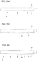
Fig. 4(a) shows abonded body 5 of the supportingsubstrate 1 andpiezoelectric material substrate 3,Fig. 4(b) shows the state that apiezoelectric material substrate 3A of a bondedbody 5A is thinned, andFig. 4(c) shows anacoustic wave device 6. -
Fig. 5(a) shows thepiezoelectric material substrate 3, andFig. 5(b) shows the state that abonding surface 12a of anintermediate layer 12 on thepiezoelectric material substrate 3 is activated. -
Fig. 6(a) shows abonded body 15 of the supportingsubstrate 1 andpiezoelectric material substrate 3,Fig. 6(b) shows the state that thepiezoelectric material substrate 3A of a bondedbody 15A is thinned by processing, andFig. 6(c) shows anacoustic wave device 16. -
Fig. 7 is a chart showing reflection characteristics of a surface acoustic wave device of the inventive example. -
Fig. 8 is a chart showing reflection characteristics of a surface acoustic wave device according to a comparative example. - Embodiments of the present invention will be described in detail below, appropriately referring to the drawings.
- First, as shown in
Fig. 2(a) , it is prepared a supportingsubstrate 1 having a pair ofmain surfaces Fig. 2(b) , abonding layer 2 is film-formed on themain surface 1a of the supportingsubstrate 1. Thesurface 2a of thebonding layer 2 is subjected to CMP polishing for obtaining a mirror surface. Then, as shown inFig.2(c) , plasma is irradiated onto thesurface 2a of thebonding layer 2 to obtain a surface-activatedbonding surface 2b. - Further, as shown in
Fig. 3(a) , it is prepared apiezoelectric material substrate 3 having amain surface 3a. Plasma is then irradiated onto the main surface of thepiezoelectric material substrate 3 as arrows C to activate the surface to form a surface-activatedbonding surface 3b. - The activated
bonding surface 2b of thebonding layer 2 on the supporting substrate and the activatedbonding surface 3b of thepiezoelectric material substrate 3 are contacted with each other and subjected to direct bonding, to obtain a bondedbody 5 shown inFig. 4(a) . - At this stage, electrodes may be provided on the
piezoelectric material substrate 3. However, preferably, as shown inFig. 4(b) , themain surface 3c of thepiezoelectric material substrate 3 is processed to thin thesubstrate 3A to form a thinnedpiezoelectric material substrate 3A so that a bondedbody 5A is provided. 9 represents a processed surface. Then, as shown inFig. 4(c) ,predetermined electrodes 10 may be formed on the processedsurface 9 of thepiezoelectric material substrate 3A of the bondedbody 5A to obtain anacoustic wave device 6. - Further, an intermediate layer may be provided between the
bonding layer 2 andpiezoelectric material substrate 3.Figs. 5 and6 relate to this embodiment. - According to the present example, as shown in
Fig. 2(a) , it is prepared a supportingsubstrate 1 having a pair ofmain surfaces Fig. 2(b) , abonding layer 2 is film-formed on themain surface 1a of the supportingsubstrate 1. The surface of thebonding layer 2 is subjected to CMP polishing for obtaining a mirror surface. Then, as shown inFig. 2(c) , plasma is irradiated onto the bonding surface of thebonding layer 2 as arrows B to obtain a surface-activatedbonding surface 2b. - Further, as shown in
Fig. 5(a) , it is prepared apiezoelectric material substrate 3 having amain surface 3a. Then, as shown inFig. 5(b) , anintermediate layer 12 is formed on the main surface (bonding surface) 3a of thepiezoelectric material substrate 3, and plasma is irradiated onto the surface of theintermediate layer 12 as arrows C to perform the surface activation to form a surface-activatedbonding surface 12a. - Then, the activated
surface 2b of thebonding layer 2 on the supporting substrate and the activatedbonding surface 12a of theintermediate layer 12 on thepiezoelectric material substrate 3 are contacted with and directly bonded with each other, to obtain a bondedbody 15 shown inFig. 6(a) . - At this stage, electrodes may be provided on the
piezoelectric material substrate 3. However, preferably, as shown inFig. 6(b) , themain surface 3c of thepiezoelectric material substrate 3 is processed to thin thesubstrate 3 to form a thinnedpiezoelectric material substrate 3A so that a bondedbody 15A is provided. 9 represents a processed surface. Then, as shown inFig. 6(c) ,predetermined electrodes 10 may be formed on the processedsurface 9 of thepiezoelectric material substrate 3A of the bondedbody 15A to obtain anacoustic wave device 16. - Alternatively, after the
bonding layer 2 is film-formed, theintermediate layer 12 may be subsequently film-formed on thebonding layer 2. In this case, CMP processing is performed on the surface of theintermediate layer 12 to obtain a bonding surface (mirror surface). Plasma is irradiated onto the thus obtained bonding surface to activate the surface. The surface of the supporting substrate is then subjected to plasma activation and directly bonded with the bonding surface of the intermediate layer. - According to the present invention, b is made 5.0 or larger. Further, b is 9.0 or smaller and may preferably be 7.0 or smaller. Further, according to the present invention, a is made 1.0×10⁻⁵ or larger, and may preferably be 1.0×10⁻⁴ or larger. Further, a is 2.0×10⁻³ or smaller and may preferably be 1.0×10⁻³ or smaller.
- According to a preferred embodiment, a and b satisfy the following formula (2).

- According to a still preferred embodiment, a and b satisfy the following formula (3).

- The measurement condition for the X-ray reflectivity method is as follows.
Measurement system: "SmartLab" supplied by Rigaku Corporation Measurement condition: X-ray generating part: Anti-cathode; Cu : Output power; 5kV 200mA Detecting part : Semiconductor detector Incident optical system : Ge(111) Unsymmetrical beam condensationcrystal Solar slit: incident side; - Reception side : 5.0 ° Slit : Reception side: IS=0.05 (mm) : Longitudinal limit: 5 (mm) : Reception side: RS1=0.1 RS2=0.1 (mm) Scanning condition : Scanning axis; 2θ/ω Scanning mode : continuous scanning Scanning speed: 0.2 ° /min Step width : 0.002 ° Analysis range : 0.3~3.0 ° - It is preferred to apply the following processing method for controlling the measurement results by the X-ray reflectivity method of the bonding surfaces of the piezoelectric material substrate and supporting substrate as described above.
- As to the method for roughening the surfaces, it is listed a mechanical processing method such as grinding process by grinding stones or blast processing by micro media such as alumina or silicon nitride, and ion beam processing of colliding ions at a high speed.
- Respective constituents of the present invention will be described further in detail below.
- Although the material of the supporting
substrate 1 is not particularly limited, the material is preferably selected from the group consisting of silicon, quartz, sialon, mullite, sapphire and translucent alumina. It is thus possible to further improve the temperature characteristics on frequency of theacoustic wave device - Although the film-forming method of the bonding layer or intermediate layer is not particularly limited, sputtering method, chemical vapor deposition (CVD) method and vapor deposition method may be listed.
- Although the material of the
bonding layer 2 is not particularly limited as far as the surface activation process is possible, a metal oxide film is preferred, and the material may preferably be selected from the group consisting of silicon oxide, silicon nitride, aluminum nitride, alumina, tantalum pentoxide, mullite, niobium pentoxide and titanium oxide. Further, as the surface activation method, an appropriate method may be selected depending on the material used for the bonding layer. Such surface activation method includes plasma activation and FAB (Ar atomic beam). - Although the material of the
intermediate layer 12 is not particularly limited as far as the surface activation processing is possible, a metal oxide film is preferred, and it is particularly preferred a material selected from the group consisting of silicon oxide, silicon nitride, aluminum nitride, alumina, tantalum pentoxide, mullite, niobium pentoxide and titanium oxide. Further, it is preferred to select the material of the intermediate layer different from that of the bonding layer. - The thickness of the
bonding layer 2 may preferably be 0.05 µm or larger, more preferably be 0.1 µm or larger and most preferably be 0.2 pm or larger on the viewpoint of the present invention. Further, the thickness of thebonding layer 2 may preferably be 3 µm or smaller, more preferably be 2 pm or smaller and further preferably be 1 pm or smaller. - The
piezoelectric material substrate 3 used in the present invention is composed of lithium tantalate (LT) single crystal, lithium niobate (LN) single crystal, or lithium niobate-lithium tantalate solid solution. As the materials have high propagation speed of an acoustic wave and large electromechanical coupling factor, they are suitable for a surface acoustic wave device of a high frequency and wide-band frequency application. - Further, although the normal line direction of the
main surface 3a of thepiezoelectric material substrate 3 is not particularly limited, for example, in the case that thepiezoelectric material substrate 3 is made of LT, it is preferred to use the substrate rotated from Y-axis toward Z-axis by 32 to 55°, (180°, 58 to 35°, 180°) on Euler angle representation, around X-axis, which is a direction of propagation of a surface acoustic wave, because of a low propagation loss. In the case that thepiezoelectric material substrate 1 is made of LN, (i) it is preferred to use the substrate rotated from Z axis toward -Y-axis by 37.8°, (0°, 37.8°, 0°) on Euler angle representation, around X-axis, which is the direction of propagation of the surface acoustic wave, because of a larger electromechanical coupling factor. Alternatively, (ii) it is preferred to use the substrate rotated from Y axis toward Z axis by 40 to 65°, (180°, 50 to 25°, 180°) on Euler angle representation, around X-axis, which is the direction of propagation of the surface acoustic wave, because of a high sound velocity. Further, although the size of thepiezoelectric material substrate 3 is not particularly limited, for example, the diameter may be 100 to 200 mm and thickness may be 0.15 to 1µm. - Plasma is then irradiated onto the bonding surfaces of the
bonding layer 2 on the supportingsubstrate 1,piezoelectric material substrate 3 andintermediate layer 12 on thepiezoelectric material substrate 3 at a temperature of 150°C or lower, to activate the bonding surfaces. On the viewpoint of the present invention, although it is preferred to irradiate nitrogen plasma, it is possible to obtain the inventive bonded body even in the case that oxygen plasma is irradiated. - The pressure during the surface activation may preferably be 100Pa or lower and more preferably be 80Pa or lower. Further, the atmosphere may be composed of nitrogen only, oxygen only or mixture of nitrogen and oxygen.
- The temperature during plasma irradiation is made 150°C or lower. It is thus possible to obtain a bonded body having a high bonding strength and without deterioration of crystallinity. On the viewpoint, the temperature during the plasma irradiation is made 150°C or lower, and may preferably be made 100°C or lower.
- Further, the energy of the plasma irradiation may preferably be 30 to 150W. Further, the product of the energy and irradiation time duration of the irradiated plasma may preferably be 0.12 to 1.0 Wh.
- The plasma-treated bonding surfaces of the piezoelectric material substrate and bonding layer are contacted with each other at room temperature. The treatment may be performed in vacuum and the contact may preferably be performed in atmosphere.
- When the activation of the surfaces is performed using the argon atomic beam, it is preferred to use a system described in
Japanese patent publication No. 2014-086400A - According to a preferred embodiment, before the surface activation treatment, the bonding surfaces of the bonding layer on the supporting substrate, of the piezoelectric material substrate and of the intermediate layer on the piezoelectric material substrate are subjected to flattening process. The method of flattening the respective surfaces includes lapping, chemical mechanical polishing (CMP) and the like. Further, the flattened surfaces may preferably have Ra of 1nm or lower and more preferably be 0.3nm or lower.
- Then, the bonding surface of the bonding layer on the supporting substrate and the bonding surface of the
piezoelectric material substrate 3 or bonding surface of the intermediate layer are contacted and bonded with each other. Thereafter, it is preferred to improve the bonding strength by performing annealing treatment. The temperature for the annealing treatment may preferably be 100°C or higher and 300°C or lower. - The bonded
bodies acoustic wave devices - Specifically, as the
acoustic wave devices - The material forming the
electrodes 10 on thepiezoelectric material substrate 3A may preferably be aluminum, aluminum alloy, copper or gold and more preferably be aluminum or aluminum alloy. The aluminum alloy used may preferably be Al doped with 0.3 to 5 weight percent of Cu. In this case, Ti, Mg, Ni, Mo, or Ta may be used instead of Cu. - It was produced an
acoustic wave device 6 shown inFig. 4(c) , according to the method described referring toFigs. 2 to 4 . - Specifically, one
main surface 3c of a 42Y-cut X-propagation LiTaO3 substrate (piezoelectric material substrate) 3 having a thickness of 250µm was polished into mirror surface and the othermain surface 3a was subjected to lapping with GC#1000. Further, it was prepared a Si(100) substrate (supporting substrate ) 1 having a thickness of 0.23mm and high resistance (>2kΩ • cm). The sizes of the respective substrates were 150mm. - The bonding surface of the supporting substrate was then subjected to processing into a roughened surface. According to the present example, it was performed grinding process using grinding stones of number of # 6000. The amount of the processing was made about 3p m.
- It was obtained the spectrum by X-ray reflectivity method of the bonding surface of the supporting substrate and the relative signal intensity was approximated based on the formula (1), to obtain values of a of 9.2×10⁻⁴ and b of 5.55.
- A
silicon oxide film 2 was the film-formed in 0.7µm on thebonding surface 1a of the supportingsubstrate 1, and the surface was polished by CMP (chemical mechanical polishing) in about 0.2um for the flattening. Then, thebonding surface 3b of thepiezoelectric material substrate 3 and bonding surface of thesilicon oxide film 2 were activated by N2 plasma, respectively, and then bonded with each other in atmosphere. Specifically, as the surface roughness of the bonding layer after the polishing was measured by AFM (Atomic force Microscope), it was confirmed that a mirror surface having Ra of 0.4nm could be obtained sufficient for the bonding. - Then, the
bonding surface 3b of thepiezoelectric material substrate 3 andbonding surface 2b of thebonding layer 2 were subjected to cleaning and surface activation, respectively. Specifically, ultrasonic cleaning by pure water was performed and the substrate surface was dried by spin drying. Then, the supporting substrate after the cleaning was introduced into a plasma activation chamber and the bonding surface of the bonding layer was activated at 30°C by nitrogen plasma. Thepiezoelectric material substrate 3 was similarly introduced in the plasma activation chamber and subjected to surface activation by nitrogen plasma at 30°C. The time period of the surface activation was made 40 seconds, and the energy was made 100W. The ultrasonic cleaning and spin drying were performed again as described above, for removing particles adhered during the surface activation. - The positions of the respective substrates were then adjusted so that the bonding surfaces of the respective activated substrates were contacted with each other at room temperature. The
piezoelectric material substrate 3 was positioned on the upper side when the substrates were contacted. As a result, it was observed the state (so-called bonding wave) that the adhesion of the substrates was spreading to prove that good preliminary bonding was accomplished. The bonded body was then charged into an oven filled with nitrogen atmosphere and held at 130°C for 40 hours, for improving the bonding strength. - The
surface 3c of thepiezoelectric material substrate 3 of the bonded body after the heating was subjected to grinding, lapping and CMP processing so that the thickness of thepiezoelectric material substrate 3A reached 7pm. - Then, for confirming the effects of the present invention, a comb-shaped electrode made of aluminum metal was formed on the piezoelectric material substrate of the bonded body, to produce a resonator of a surface acoustic wave device. The specification was shown as follows.
IDT period: 6µm IDT opening length: 300um Number of IDT lines: 80 lines Number of lines of reflector: 40 lines - As the reflection characteristics of the resonator was measured by a network analyzer, spurious was hardly observed in a range higher than an anti-resonance frequency, as shown in
Fig. 7 . The value of the spurious wave was proved to be 2.7dB. - The results were shown in table 1.
- It was produced the resonator of the surface acoustic wave device according to the same procedure as that in the inventive example 1, and the reflection characteristics of the resonator was measured by the network analyzer. However, the processing of the bonding surface of the supporting substrate was performed by grinding the bonding surface by grinding stones of # 8000.
- As spectrum of the bonding surface of the supporting substrate was obtained by X-ray reflectivity method and the relative signal intensity was approximated by the formula (1), it was obtained a of 7.1×10⁻⁴ and b of 5.80. The magnitude of the spurious wave was proved to be 3.2dB.
- It was produced the resonator of the surface acoustic wave device according to the same procedure as the inventive example 1, and the reflection characteristics of the resonator was measured by the network analyzer. However, the processing of the bonding layer of the supporting substrate was performed by blasting of the whole surface of the substrate by silicon nitride particles. The amount of the processing was evaluated and proved to be as small as 10nm.
- As spectrum of the bonding surface of the supporting substrate was obtained by X-ray reflectivity method and the relative signal intensity was approximated by the formula (1), it was obtained a of 2.2×10⁻⁵ and b of 8.84. The magnitude of the spurious wave was proved to be 4.8dB.
- The resonator of the surface acoustic wave device was produced according to the same procedure as that of the inventive example 1, and the reflection characteristics of the resonator was measured by the network analyzer. However, the processing of the bonding surface of the supporting substrate was performed by charging the supporting substrate in an ion processing machine and by colliding Ar ions accelerated at 0.5keV.
- As spectrum of the bonding surface of the supporting substrate was obtained by X-ray reflectivity method and the relative signal intensity was approximated by the formula (1), it was obtained a of 5.6×10⁻⁵ and b of 7.63. The magnitude of the spurious wave was proved to be 3.3dB.
- The resonator of the surface acoustic wave device was produced according to the same procedure as that of the inventive example 1, and the reflection characteristics of the resonator was measured by the network analyzer. However, the processing of the bonding surface was performed by charging the supporting substrate in an ion processing machine and by colliding Ar ions accelerated at 1.0keV.
- As spectrum of the bonding surface of the supporting substrate was obtained by X-ray reflectivity method and the relative signal intensity was approximated by the formula (1), it was obtained a of 1.8×10⁻³ and b of 5.12. The magnitude of the spurious wave was proved to be 3.5dB.
- The resonator of the surface acoustic wave device was produced according to the same procedure as that of the inventive example 1, and the reflection characteristics of the resonator was measured by the network analyzer. However, as the bonding surface of the supporting substrate was made a mirror surface, Ra was 0.02nm and the approximation by the formula (1) could not be made. Spurious was observed in the reflection characteristics, as shown in
Fig. 8 . The magnitude of the spurious wave was 12dB.Table 1 a b Spurious (dB) Inventive Example 1 9.2×10⁻⁴ 5.55 2.7 Inventive Example 2 7.1×10⁻⁴ 5.80 3.2 Inventive Example 3 2.2×10⁻⁵ 8.84 4.8 Inventive Example 4 5.6×10⁻⁵ 7.63 3.3 Inventive Example 5 1.8×10⁻³ 5.12 3.5 Comparative Example 1 --- --- 12
Claims (2)
- A bonded body comprising:a supporting substrate;a piezoelectric material substrate comprising a material selected from the group consisting of lithium niobate, lithium tantalate and lithium niobate-lithium tantalate; anda bonding layer bonding said supporting substrate and said piezoelectric material substrate,provided that at least one of a bonding surface of said supporting substrate and a bonding surface of said piezoelectric material substrate is measured by X-ray reflectivity method and that 1 is assigned to a signal intensity in the case of total reflection, a relative intensity I of a reflected light from said bonding surface is approximated by the following formula (1) in a range of 1.0×10⁻⁴ or larger and 1.0×10⁻¹ or smaller.
 θ represents an incident angle of an X-ray with respect to said bonding surface,a is 1.0×10⁻⁵ or larger and 2.0×10⁻³ or smaller, andb is 5.0 or larger and 9.0 or smaller.)
 - The bonded body of claim 1, wherein said bonding layer comprises a material selected from the group consisting of silicon oxide, silicon nitride, aluminum nitride, alumina, tantalum pentoxide, mullite, niobium pentoxide and titanium oxide.
Applications Claiming Priority (2)
| Application Number | Priority Date | Filing Date | Title |
|---|---|---|---|
| JP2019216520 | 2019-11-29 | ||
| PCT/JP2020/042099 WO2021106572A1 (en) | 2019-11-29 | 2020-11-11 | Joined body of piezoelectric material substrate and support substrate |
Publications (3)
| Publication Number | Publication Date |
|---|---|
| EP4068625A1 true EP4068625A1 (en) | 2022-10-05 |
| EP4068625A4 EP4068625A4 (en) | 2023-05-24 |
| EP4068625B1 EP4068625B1 (en) | 2025-01-29 |
Family
ID=76130103
Family Applications (1)
| Application Number | Title | Priority Date | Filing Date |
|---|---|---|---|
| EP20893072.7A Active EP4068625B1 (en) | 2019-11-29 | 2020-11-11 | Bonded body comprising piezoelectric material substrate and support substrate |
Country Status (7)
| Country | Link |
|---|---|
| US (1) | US11791795B2 (en) |
| EP (1) | EP4068625B1 (en) |
| JP (1) | JP6951607B1 (en) |
| KR (1) | KR102402296B1 (en) |
| CN (1) | CN114731150B (en) |
| TW (1) | TWI812902B (en) |
| WO (1) | WO2021106572A1 (en) |
Family Cites Families (14)
| Publication number | Priority date | Publication date | Assignee | Title |
|---|---|---|---|---|
| US4348724A (en) | 1980-04-15 | 1982-09-07 | Honeywell Information Systems Inc. | Address pairing apparatus for a control store of a data processing system |
| JP2003121133A (en) | 2001-10-17 | 2003-04-23 | Acbtec:Kk | Method and apparatus for forming multilayer thin film |
| WO2011046117A1 (en) * | 2009-10-13 | 2011-04-21 | 株式会社村田製作所 | Elastic surface-wave device |
| JP2014086400A (en) | 2012-10-26 | 2014-05-12 | Mitsubishi Heavy Ind Ltd | High speed atom beam source and normal temperature bonding device including the same |
| US10523178B2 (en) | 2015-08-25 | 2019-12-31 | Avago Technologies International Sales Pte. Limited | Surface acoustic wave (SAW) resonator |
| KR20170063333A (en) | 2015-11-27 | 2017-06-08 | 한국전자통신연구원 | photo-acoustic probe and photo-acoustic measurement apparatus including the same |
| CN105420674A (en) * | 2015-12-04 | 2016-03-23 | 济南晶正电子科技有限公司 | Single-crystal film bonding body and manufacturing method thereof |
| KR20180107212A (en) * | 2016-03-25 | 2018-10-01 | 엔지케이 인슐레이터 엘티디 | Joining method |
| WO2017163723A1 (en) * | 2016-03-25 | 2017-09-28 | 日本碍子株式会社 | Bonding method |
| JP6250856B1 (en) * | 2016-07-20 | 2017-12-20 | 信越化学工業株式会社 | Composite substrate for surface acoustic wave device, manufacturing method thereof, and surface acoustic wave device using the composite substrate |
| JP6621384B2 (en) * | 2016-07-20 | 2019-12-18 | 信越化学工業株式会社 | Method for manufacturing composite substrate for surface acoustic wave device |
| CN110945787B (en) * | 2017-08-25 | 2023-06-02 | 日本碍子株式会社 | Bonded body and elastic wave element |
| GB201714646D0 (en) | 2017-09-12 | 2017-10-25 | Spts Technologies Ltd | Saw device and method of manufacture |
| EP3771099B1 (en) * | 2018-03-20 | 2024-04-03 | NGK Insulators, Ltd. | Bonded body of piezoelectric material substrate and supporting substrate |
-
2020
- 2020-11-11 CN CN202080005724.9A patent/CN114731150B/en active Active
- 2020-11-11 EP EP20893072.7A patent/EP4068625B1/en active Active
- 2020-11-11 KR KR1020217019298A patent/KR102402296B1/en active Active
- 2020-11-11 WO PCT/JP2020/042099 patent/WO2021106572A1/en not_active Ceased
- 2020-11-11 JP JP2021504324A patent/JP6951607B1/en active Active
- 2020-11-27 TW TW109141741A patent/TWI812902B/en active
-
2021
- 2021-06-25 US US17/358,121 patent/US11791795B2/en active Active
Also Published As
| Publication number | Publication date |
|---|---|
| EP4068625B1 (en) | 2025-01-29 |
| CN114731150A (en) | 2022-07-08 |
| EP4068625A4 (en) | 2023-05-24 |
| CN114731150B (en) | 2025-09-30 |
| JP6951607B1 (en) | 2021-10-20 |
| JPWO2021106572A1 (en) | 2021-12-02 |
| US20210328569A1 (en) | 2021-10-21 |
| TW202127016A (en) | 2021-07-16 |
| WO2021106572A1 (en) | 2021-06-03 |
| TWI812902B (en) | 2023-08-21 |
| US11791795B2 (en) | 2023-10-17 |
| KR102402296B1 (en) | 2022-05-26 |
| KR20210084645A (en) | 2021-07-07 |
Similar Documents
| Publication | Publication Date | Title |
|---|---|---|
| US12101079B2 (en) | Method of producing a bonded body of piezoelectric material substrate | |
| US12323127B2 (en) | Composite substrate, elastic wave element, and production method for composite substrate | |
| US11632093B2 (en) | Acoustic wave devices and a method of producing the same | |
| US11133788B2 (en) | Bonded body and elastic wave element | |
| US12237824B2 (en) | Composite substrate, elastic wave element, and production method for composite substrate | |
| KR20200144148A (en) | Assembly of piezoelectric material substrate and support substrate | |
| WO2019220713A1 (en) | Joined body of piezoelectric single-crystal substrate and support substrate | |
| EP4117180B1 (en) | Joined structure | |
| US20220399873A1 (en) | Composite substrate and method of producing composite substrate | |
| EP4068624B1 (en) | Bonded body comprising piezoelectric material substrate and support substrate | |
| US11700771B2 (en) | Assembly of piezoelectric material substrate and support substrate, and method for manufacturing said assembly | |
| US12395146B2 (en) | Composite substrate for acoustic wave device | |
| EP4068625B1 (en) | Bonded body comprising piezoelectric material substrate and support substrate | |
| KR20220156894A (en) | Conjugate and manufacturing method thereof |
Legal Events
| Date | Code | Title | Description |
|---|---|---|---|
| STAA | Information on the status of an ep patent application or granted ep patent |
Free format text: STATUS: THE INTERNATIONAL PUBLICATION HAS BEEN MADE |
|
| PUAI | Public reference made under article 153(3) epc to a published international application that has entered the european phase |
Free format text: ORIGINAL CODE: 0009012 |
|
| STAA | Information on the status of an ep patent application or granted ep patent |
Free format text: STATUS: REQUEST FOR EXAMINATION WAS MADE |
|
| 17P | Request for examination filed |
Effective date: 20220623 |
|
| AK | Designated contracting states |
Kind code of ref document: A1 Designated state(s): AL AT BE BG CH CY CZ DE DK EE ES FI FR GB GR HR HU IE IS IT LI LT LU LV MC MK MT NL NO PL PT RO RS SE SI SK SM TR |
|
| DAV | Request for validation of the european patent (deleted) | ||
| DAX | Request for extension of the european patent (deleted) | ||
| REG | Reference to a national code |
Ref legal event code: R079 Free format text: PREVIOUS MAIN CLASS: H03H0003080000 Ipc: H10N0030073000 Ref country code: DE Ref legal event code: R079 Ref document number: 602020045645 Country of ref document: DE Free format text: PREVIOUS MAIN CLASS: H03H0003080000 Ipc: H10N0030073000 |
|
| A4 | Supplementary search report drawn up and despatched |
Effective date: 20230426 |
|
| RIC1 | Information provided on ipc code assigned before grant |
Ipc: G01N 23/20 20180101ALN20230420BHEP Ipc: H03H 9/02 20060101ALI20230420BHEP Ipc: H03H 3/08 20060101ALI20230420BHEP Ipc: H10N 30/073 20230101AFI20230420BHEP |
|
| STAA | Information on the status of an ep patent application or granted ep patent |
Free format text: STATUS: EXAMINATION IS IN PROGRESS |
|
| 17Q | First examination report despatched |
Effective date: 20240222 |
|
| GRAP | Despatch of communication of intention to grant a patent |
Free format text: ORIGINAL CODE: EPIDOSNIGR1 |
|
| STAA | Information on the status of an ep patent application or granted ep patent |
Free format text: STATUS: GRANT OF PATENT IS INTENDED |
|
| INTG | Intention to grant announced |
Effective date: 20240930 |
|
| GRAS | Grant fee paid |
Free format text: ORIGINAL CODE: EPIDOSNIGR3 |
|
| GRAA | (expected) grant |
Free format text: ORIGINAL CODE: 0009210 |
|
| STAA | Information on the status of an ep patent application or granted ep patent |
Free format text: STATUS: THE PATENT HAS BEEN GRANTED |
|
| AK | Designated contracting states |
Kind code of ref document: B1 Designated state(s): AL AT BE BG CH CY CZ DE DK EE ES FI FR GB GR HR HU IE IS IT LI LT LU LV MC MK MT NL NO PL PT RO RS SE SI SK SM TR |
|
| REG | Reference to a national code |
Ref country code: GB Ref legal event code: FG4D |
|
| REG | Reference to a national code |
Ref country code: CH Ref legal event code: EP |
|
| REG | Reference to a national code |
Ref country code: DE Ref legal event code: R096 Ref document number: 602020045645 Country of ref document: DE |
|
| REG | Reference to a national code |
Ref country code: IE Ref legal event code: FG4D |
|
| REG | Reference to a national code |
Ref country code: NL Ref legal event code: MP Effective date: 20250129 |
|
| PG25 | Lapsed in a contracting state [announced via postgrant information from national office to epo] |
Ref country code: NL Free format text: LAPSE BECAUSE OF FAILURE TO SUBMIT A TRANSLATION OF THE DESCRIPTION OR TO PAY THE FEE WITHIN THE PRESCRIBED TIME-LIMIT Effective date: 20250129 |
|
| PG25 | Lapsed in a contracting state [announced via postgrant information from national office to epo] |
Ref country code: RS Free format text: LAPSE BECAUSE OF FAILURE TO SUBMIT A TRANSLATION OF THE DESCRIPTION OR TO PAY THE FEE WITHIN THE PRESCRIBED TIME-LIMIT Effective date: 20250429 |
|
| PG25 | Lapsed in a contracting state [announced via postgrant information from national office to epo] |
Ref country code: FI Free format text: LAPSE BECAUSE OF FAILURE TO SUBMIT A TRANSLATION OF THE DESCRIPTION OR TO PAY THE FEE WITHIN THE PRESCRIBED TIME-LIMIT Effective date: 20250129 |
|
| PG25 | Lapsed in a contracting state [announced via postgrant information from national office to epo] |
Ref country code: PL Free format text: LAPSE BECAUSE OF FAILURE TO SUBMIT A TRANSLATION OF THE DESCRIPTION OR TO PAY THE FEE WITHIN THE PRESCRIBED TIME-LIMIT Effective date: 20250129 |
|
| PG25 | Lapsed in a contracting state [announced via postgrant information from national office to epo] |
Ref country code: ES Free format text: LAPSE BECAUSE OF FAILURE TO SUBMIT A TRANSLATION OF THE DESCRIPTION OR TO PAY THE FEE WITHIN THE PRESCRIBED TIME-LIMIT Effective date: 20250129 |
|
| REG | Reference to a national code |
Ref country code: LT Ref legal event code: MG9D |
|
| PG25 | Lapsed in a contracting state [announced via postgrant information from national office to epo] |
Ref country code: IS Free format text: LAPSE BECAUSE OF FAILURE TO SUBMIT A TRANSLATION OF THE DESCRIPTION OR TO PAY THE FEE WITHIN THE PRESCRIBED TIME-LIMIT Effective date: 20250529 Ref country code: NO Free format text: LAPSE BECAUSE OF FAILURE TO SUBMIT A TRANSLATION OF THE DESCRIPTION OR TO PAY THE FEE WITHIN THE PRESCRIBED TIME-LIMIT Effective date: 20250429 |
|
| REG | Reference to a national code |
Ref country code: AT Ref legal event code: MK05 Ref document number: 1764711 Country of ref document: AT Kind code of ref document: T Effective date: 20250129 |
|
| PG25 | Lapsed in a contracting state [announced via postgrant information from national office to epo] |
Ref country code: HR Free format text: LAPSE BECAUSE OF FAILURE TO SUBMIT A TRANSLATION OF THE DESCRIPTION OR TO PAY THE FEE WITHIN THE PRESCRIBED TIME-LIMIT Effective date: 20250129 |
|
| PG25 | Lapsed in a contracting state [announced via postgrant information from national office to epo] |
Ref country code: LV Free format text: LAPSE BECAUSE OF FAILURE TO SUBMIT A TRANSLATION OF THE DESCRIPTION OR TO PAY THE FEE WITHIN THE PRESCRIBED TIME-LIMIT Effective date: 20250129 Ref country code: PT Free format text: LAPSE BECAUSE OF FAILURE TO SUBMIT A TRANSLATION OF THE DESCRIPTION OR TO PAY THE FEE WITHIN THE PRESCRIBED TIME-LIMIT Effective date: 20250529 |
|
| PG25 | Lapsed in a contracting state [announced via postgrant information from national office to epo] |
Ref country code: GR Free format text: LAPSE BECAUSE OF FAILURE TO SUBMIT A TRANSLATION OF THE DESCRIPTION OR TO PAY THE FEE WITHIN THE PRESCRIBED TIME-LIMIT Effective date: 20250430 Ref country code: BG Free format text: LAPSE BECAUSE OF FAILURE TO SUBMIT A TRANSLATION OF THE DESCRIPTION OR TO PAY THE FEE WITHIN THE PRESCRIBED TIME-LIMIT Effective date: 20250129 |
|
| PG25 | Lapsed in a contracting state [announced via postgrant information from national office to epo] |
Ref country code: AT Free format text: LAPSE BECAUSE OF FAILURE TO SUBMIT A TRANSLATION OF THE DESCRIPTION OR TO PAY THE FEE WITHIN THE PRESCRIBED TIME-LIMIT Effective date: 20250129 |
|
| PG25 | Lapsed in a contracting state [announced via postgrant information from national office to epo] |
Ref country code: SE Free format text: LAPSE BECAUSE OF FAILURE TO SUBMIT A TRANSLATION OF THE DESCRIPTION OR TO PAY THE FEE WITHIN THE PRESCRIBED TIME-LIMIT Effective date: 20250129 |
|
| PG25 | Lapsed in a contracting state [announced via postgrant information from national office to epo] |
Ref country code: SM Free format text: LAPSE BECAUSE OF FAILURE TO SUBMIT A TRANSLATION OF THE DESCRIPTION OR TO PAY THE FEE WITHIN THE PRESCRIBED TIME-LIMIT Effective date: 20250129 |
|
| PG25 | Lapsed in a contracting state [announced via postgrant information from national office to epo] |
Ref country code: DK Free format text: LAPSE BECAUSE OF FAILURE TO SUBMIT A TRANSLATION OF THE DESCRIPTION OR TO PAY THE FEE WITHIN THE PRESCRIBED TIME-LIMIT Effective date: 20250129 |
|
| PG25 | Lapsed in a contracting state [announced via postgrant information from national office to epo] |
Ref country code: IT Free format text: LAPSE BECAUSE OF FAILURE TO SUBMIT A TRANSLATION OF THE DESCRIPTION OR TO PAY THE FEE WITHIN THE PRESCRIBED TIME-LIMIT Effective date: 20250129 |
|
| PG25 | Lapsed in a contracting state [announced via postgrant information from national office to epo] |
Ref country code: CZ Free format text: LAPSE BECAUSE OF FAILURE TO SUBMIT A TRANSLATION OF THE DESCRIPTION OR TO PAY THE FEE WITHIN THE PRESCRIBED TIME-LIMIT Effective date: 20250129 Ref country code: EE Free format text: LAPSE BECAUSE OF FAILURE TO SUBMIT A TRANSLATION OF THE DESCRIPTION OR TO PAY THE FEE WITHIN THE PRESCRIBED TIME-LIMIT Effective date: 20250129 |
|
| PG25 | Lapsed in a contracting state [announced via postgrant information from national office to epo] |
Ref country code: RO Free format text: LAPSE BECAUSE OF FAILURE TO SUBMIT A TRANSLATION OF THE DESCRIPTION OR TO PAY THE FEE WITHIN THE PRESCRIBED TIME-LIMIT Effective date: 20250129 |
|
| PG25 | Lapsed in a contracting state [announced via postgrant information from national office to epo] |
Ref country code: SK Free format text: LAPSE BECAUSE OF FAILURE TO SUBMIT A TRANSLATION OF THE DESCRIPTION OR TO PAY THE FEE WITHIN THE PRESCRIBED TIME-LIMIT Effective date: 20250129 |
|
| REG | Reference to a national code |
Ref country code: DE Ref legal event code: R097 Ref document number: 602020045645 Country of ref document: DE |
|
| PLBE | No opposition filed within time limit |
Free format text: ORIGINAL CODE: 0009261 |
|
| STAA | Information on the status of an ep patent application or granted ep patent |
Free format text: STATUS: NO OPPOSITION FILED WITHIN TIME LIMIT |
|
| REG | Reference to a national code |
Ref country code: CH Ref legal event code: L10 Free format text: ST27 STATUS EVENT CODE: U-0-0-L10-L00 (AS PROVIDED BY THE NATIONAL OFFICE) Effective date: 20251210 |
|
| 26N | No opposition filed |
Effective date: 20251030 |
|
| PGFP | Annual fee paid to national office [announced via postgrant information from national office to epo] |
Ref country code: DE Payment date: 20250930 Year of fee payment: 6 |
|
| REG | Reference to a national code |
Ref country code: CH Ref legal event code: H13 Free format text: ST27 STATUS EVENT CODE: U-0-0-H10-H13 (AS PROVIDED BY THE NATIONAL OFFICE) Effective date: 20260623 |
|
| PG25 | Lapsed in a contracting state [announced via postgrant information from national office to epo] |
Ref country code: LT Free format text: LAPSE BECAUSE OF FAILURE TO SUBMIT A TRANSLATION OF THE DESCRIPTION OR TO PAY THE FEE WITHIN THE PRESCRIBED TIME-LIMIT Effective date: 20250129 |
|
| PG25 | Lapsed in a contracting state [announced via postgrant information from national office to epo] |
Ref country code: MC Free format text: LAPSE BECAUSE OF FAILURE TO SUBMIT A TRANSLATION OF THE DESCRIPTION OR TO PAY THE FEE WITHIN THE PRESCRIBED TIME-LIMIT Effective date: 20250129 |
|
| PG25 | Lapsed in a contracting state [announced via postgrant information from national office to epo] |
Ref country code: LU Free format text: LAPSE BECAUSE OF NON-PAYMENT OF DUE FEES Effective date: 20251111 Ref country code: CH Free format text: LAPSE BECAUSE OF NON-PAYMENT OF DUE FEES Effective date: 20251130 |