EP4068525A1 - Connector and electronic device - Google Patents
Connector and electronic device Download PDFInfo
- Publication number
- EP4068525A1 EP4068525A1 EP20893508.0A EP20893508A EP4068525A1 EP 4068525 A1 EP4068525 A1 EP 4068525A1 EP 20893508 A EP20893508 A EP 20893508A EP 4068525 A1 EP4068525 A1 EP 4068525A1
- Authority
- EP
- European Patent Office
- Prior art keywords
- insulator
- movable insulator
- movable
- contact
- connector
- Prior art date
- Legal status (The legal status is an assumption and is not a legal conclusion. Google has not performed a legal analysis and makes no representation as to the accuracy of the status listed.)
- Granted
Links
Images





Classifications
-
- H—ELECTRICITY
- H01—ELECTRIC ELEMENTS
- H01R—ELECTRICALLY-CONDUCTIVE CONNECTIONS; STRUCTURAL ASSOCIATIONS OF A PLURALITY OF MUTUALLY-INSULATED ELECTRICAL CONNECTING ELEMENTS; COUPLING DEVICES; CURRENT COLLECTORS
- H01R12/00—Structural associations of a plurality of mutually-insulated electrical connecting elements, specially adapted for printed circuits, e.g. printed circuit boards [PCB], flat or ribbon cables, or like generally planar structures, e.g. terminal strips, terminal blocks; Coupling devices specially adapted for printed circuits, flat or ribbon cables, or like generally planar structures; Terminals specially adapted for contact with, or insertion into, printed circuits, flat or ribbon cables, or like generally planar structures
- H01R12/70—Coupling devices
- H01R12/71—Coupling devices for rigid printing circuits or like structures
- H01R12/72—Coupling devices for rigid printing circuits or like structures coupling with the edge of the rigid printed circuits or like structures
- H01R12/722—Coupling devices for rigid printing circuits or like structures coupling with the edge of the rigid printed circuits or like structures coupling devices mounted on the edge of the printed circuits
- H01R12/728—Coupling devices without an insulating housing provided on the edge of the PCB
-
- H—ELECTRICITY
- H01—ELECTRIC ELEMENTS
- H01R—ELECTRICALLY-CONDUCTIVE CONNECTIONS; STRUCTURAL ASSOCIATIONS OF A PLURALITY OF MUTUALLY-INSULATED ELECTRICAL CONNECTING ELEMENTS; COUPLING DEVICES; CURRENT COLLECTORS
- H01R12/00—Structural associations of a plurality of mutually-insulated electrical connecting elements, specially adapted for printed circuits, e.g. printed circuit boards [PCB], flat or ribbon cables, or like generally planar structures, e.g. terminal strips, terminal blocks; Coupling devices specially adapted for printed circuits, flat or ribbon cables, or like generally planar structures; Terminals specially adapted for contact with, or insertion into, printed circuits, flat or ribbon cables, or like generally planar structures
- H01R12/70—Coupling devices
- H01R12/91—Coupling devices allowing relative movement between coupling parts, e.g. floating or self aligning
-
- H—ELECTRICITY
- H01—ELECTRIC ELEMENTS
- H01R—ELECTRICALLY-CONDUCTIVE CONNECTIONS; STRUCTURAL ASSOCIATIONS OF A PLURALITY OF MUTUALLY-INSULATED ELECTRICAL CONNECTING ELEMENTS; COUPLING DEVICES; CURRENT COLLECTORS
- H01R12/00—Structural associations of a plurality of mutually-insulated electrical connecting elements, specially adapted for printed circuits, e.g. printed circuit boards [PCB], flat or ribbon cables, or like generally planar structures, e.g. terminal strips, terminal blocks; Coupling devices specially adapted for printed circuits, flat or ribbon cables, or like generally planar structures; Terminals specially adapted for contact with, or insertion into, printed circuits, flat or ribbon cables, or like generally planar structures
- H01R12/70—Coupling devices
- H01R12/71—Coupling devices for rigid printing circuits or like structures
- H01R12/712—Coupling devices for rigid printing circuits or like structures co-operating with the surface of the printed circuit or with a coupling device exclusively provided on the surface of the printed circuit
- H01R12/716—Coupling device provided on the PCB
-
- H—ELECTRICITY
- H01—ELECTRIC ELEMENTS
- H01R—ELECTRICALLY-CONDUCTIVE CONNECTIONS; STRUCTURAL ASSOCIATIONS OF A PLURALITY OF MUTUALLY-INSULATED ELECTRICAL CONNECTING ELEMENTS; COUPLING DEVICES; CURRENT COLLECTORS
- H01R13/00—Details of coupling devices of the kinds covered by groups H01R12/70 or H01R24/00 - H01R33/00
- H01R13/46—Bases; Cases
- H01R13/502—Bases; Cases composed of different pieces
-
- H—ELECTRICITY
- H01—ELECTRIC ELEMENTS
- H01R—ELECTRICALLY-CONDUCTIVE CONNECTIONS; STRUCTURAL ASSOCIATIONS OF A PLURALITY OF MUTUALLY-INSULATED ELECTRICAL CONNECTING ELEMENTS; COUPLING DEVICES; CURRENT COLLECTORS
- H01R12/00—Structural associations of a plurality of mutually-insulated electrical connecting elements, specially adapted for printed circuits, e.g. printed circuit boards [PCB], flat or ribbon cables, or like generally planar structures, e.g. terminal strips, terminal blocks; Coupling devices specially adapted for printed circuits, flat or ribbon cables, or like generally planar structures; Terminals specially adapted for contact with, or insertion into, printed circuits, flat or ribbon cables, or like generally planar structures
- H01R12/70—Coupling devices
- H01R12/71—Coupling devices for rigid printing circuits or like structures
- H01R12/72—Coupling devices for rigid printing circuits or like structures coupling with the edge of the rigid printed circuits or like structures
- H01R12/73—Coupling devices for rigid printing circuits or like structures coupling with the edge of the rigid printed circuits or like structures connecting to other rigid printed circuits or like structures
-
- H—ELECTRICITY
- H01—ELECTRIC ELEMENTS
- H01R—ELECTRICALLY-CONDUCTIVE CONNECTIONS; STRUCTURAL ASSOCIATIONS OF A PLURALITY OF MUTUALLY-INSULATED ELECTRICAL CONNECTING ELEMENTS; COUPLING DEVICES; CURRENT COLLECTORS
- H01R13/00—Details of coupling devices of the kinds covered by groups H01R12/70 or H01R24/00 - H01R33/00
- H01R13/46—Bases; Cases
- H01R13/514—Bases; Cases composed as a modular blocks or assembly, i.e. composed of co-operating parts provided with contact members or holding contact members between them
Definitions
- the present disclosure relates to a connector, and an electronic apparatus.
- Connectors with a floating structure are known in the art as an exemplary technique for improving the reliability of connection with a connection object, which is an object to be connected.
- the floating structure allows a part of such a connector to move even during and after mating to thereby absorb misalignment between the connection object and the connector.
- PTL 1 discloses an electrical connector that contributes to miniaturization while preventing or reducing poor conduction caused by rising of flux.
- the movable insulator includes a first movable insulator and a second movable insulator that are disposed inside the fixed insulator while being separated from each other.
- the first movable insulator and the second movable insulator are capable of moving independently of each other.
- An electronic apparatus includes the connector described above.
- connection object moves when the connection object and the connector are in their mated condition, a load such as stress is exerted on a movable insulator and a fixed insulator that are in mating engagement with the connection object.
- a load such as stress is exerted on a movable insulator and a fixed insulator that are in mating engagement with the connection object.
- Such load increases as, for example, the connector increases in length due to an increase in the number of poles. Accordingly, such a connector with a floating structure needs to be designed to mitigate this load.
- the design of the electrical connector described in PTL 1 does not give adequate consideration to a structure that allows for mitigation of the above-mentioned load.
- a connector and an electronic apparatus make it possible to mitigate the load that is exerted on a movable insulator and a fixed insulator of the connector having a floating structure when these insulators are in mating engagement with the connection object.
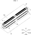
- Fig. 1 is a top exterior perspective view of a connector 10 according to an embodiment with a connection object 60 connected to the connector 10.
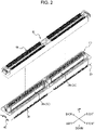
- Fig. 2 is a top exterior perspective view of the connector 10 according to the embodiment when separated from the connection object 60.
- the connector 10 includes a fixed insulator 20, a first movable insulator 30a, a second movable insulator 30b, a metal fitting 40, and contacts 50.
- the first movable insulator 30a and the second movable insulator 30b will be collectively referred to as "movable insulator 30" or "movable insulators 30" when no distinction is made between these individual movable insulators.
- the connector 10 according to the embodiment will be described as being a receptacle connector.
- the connection object 60 will be described as being a plug connector.
- the connector 10 whose contacts 50 undergo elastic deformation will be described as a receptacle connector
- the connection object 60 whose contacts 90 described later do not undergo elastic deformation will be described as a plug connector.
- the types of the connector 10 and the connection object 60 are not limited to those mentioned above.
- the connector 10 may serve as a plug connector
- the connection object 60 may serve as a receptacle connector.
- the connector 10 and the connection object 60 will be described below as being respectively mounted to a circuit board CB1 and a circuit board CB2.
- the connector 10 provides electrical connection between the connection object 60 mated with the connector 10, and the circuit board CB1.
- the connector 10 provides electrical connection between the circuit board CB2 on which the connection object 60 is mounted, and the circuit board CB1.
- the circuit boards CB1 and CB2 may be rigid boards or any other circuit boards.
- at least one of the circuit board CB1 and the circuit board CB2 may be a flexible printed circuit board (FPC) .
- the connector 10 and the connection object 60 will be described below as being connected to each other in a direction perpendicular to the circuit boards CB1 and CB2.
- the connector 10 and the connection object 60 are connected to each other in the up-down direction.
- the connector 10 and the connection object 60 may not necessarily be connected as described above.
- the connector 10 and the connection object 60 may be connected to each other in a direction parallel to the circuit boards CB1 and CB2.
- the connector 10 and the connection object 60 may be connected to each other such that one of the connector 10 and the connection object 60 is perpendicular to the circuit board on which the one of the connector 10 and the connection object 60 is mounted, and the other one of the connector 10 and the connection object 60 is parallel to the circuit board on which the other one of the connector 10 and the connection object 60 is mounted.
- the term “mating direction” means, for example, the up-down or vertical direction.
- the term “mating side” refers to, for example, the upper side.
- the term “protruding direction” refers to, for example, the left-right direction.
- the term “direction of arrangement of the contacts 50" refers to, for example, the left-right direction.
- the connector 10 according to an embodiment has a floating structure.
- the connector 10 allows the connection object 60 connected with the connector 10 to move relative to the circuit board CB1.
- the connection object 60 is capable of moving within a predetermined range relative to the circuit board CB1 even when the connection object 60 is being connected with the connector 10.
- Fig. 3 is a top exterior perspective view of the connector 10 illustrated in in Fig. 1 with the connector 10 shown alone.
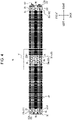
- Fig. 4 is a bottom view of the connector 10 illustrated in Fig. 1 with the connector 10 shown alone.
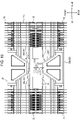
- Fig. 5 is an enlarged view of a portion V bounded by dashed lines illustrated in Fig. 4 .
- Fig. 6 is a top exploded perspective view of the connector 10 illustrated in Fig. 3 .
- Fig. 7 is a cross-sectional perspective view taken along an arrow line VII-VII illustrated in Fig. 3 .
- Fig. 8 is an enlarged view of a portion VIII bounded by dashed lines illustrated in Fig. 7 .
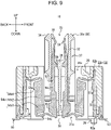
- FIG. 9 is a cross-sectional view taken along the arrow line VII-VII illustrated in Fig. 3 .
- Fig. 10 is a front view of a pair of contacts 50 illustrated in Fig. 6 .
- Fig. 11 is an enlarged view of a portion XI bounded by dashed lines illustrated in Fig. 10 .
- the arrow line VII-VII is depicted in Fig. 3 as being positioned over, for example, the first movable insulator 30a of the movable insulator 30, the same cross-sections as those illustrated in Figs. 7 to 9 are obtained also for the second movable insulator 30b. Accordingly, the description given below with respect to the first movable insulator 30a similarly applies to the second movable insulator 30b.
- the connector 10 is assembled as described below.
- the metal fitting 40 is press-fit into the fixed insulator 20 from below, and the movable insulator 30 is disposed inside the fixed insulator 20 into which the metal fitting 40 has been press-fit.
- Each contact 50 is press-fit into the fixed insulator 20 and the movable insulator 30 from below.
- the fixed insulator 20 is a rectangular tubular component that is injection molded from a synthetic resin material having insulating and heat-resistant properties.
- the fixed insulator 20 is in the shape of a hollow frame.
- the fixed insulator 20 has, on the top side, a first opening 21a and a second opening 21b.
- the fixed insulator 20 has a third opening 21c on the bottom side.
- the fixed insulator 20 has an outer periphery wall 22.
- the outer periphery wall 22 includes four side walls on the front, back, left, and right sides, and surrounds the space inside the fixed insulator 20.
- the outer periphery wall 22 includes a pair of lateral walls 22a on the left and right sides, and a pair of longitudinal walls 22b on the front and back sides.
- Each longitudinal wall 22b has a protruding wall 22b1 provided at the left and right ends and in the middle of the longitudinal wall 22b.
- the protruding wall 22b1 protrudes inward in the front-back direction.
- the fixed insulator 20 has a metal-fitting attachment groove 23.
- the metal-fitting attachment groove 23 is defined in the lateral wall 22a so as to extend vertically, and provided inside the fixed insulator 20.
- the metal fitting 40 is attached to the metal-fitting attachment groove 23.
- the fixed insulator 20 has multiple contact attachment grooves 24 defined on the inner side of the longitudinal wall 22b such that the contact attachment grooves 24 extend from the lower edge to the bottom and inner surfaces.
- the contact attachment grooves 24 are spaced from each other at predetermined intervals in the left-right direction.
- Each contact attachment groove 24 extends vertically on the longitudinal wall 22b of the fixed insulator 20.
- the contact 50 is attached to the contact attachment groove 24.
- the fixed insulator 20 has a division wall 25 in the middle part of the longitudinal wall 22b.
- the division wall 25 extends in the front-back direction so as to couple the longitudinal wall 22b on the front side and the longitudinal wall 22b on the back side to each other.
- the division wall 25 divides, in the middle part of the longitudinal wall 22b, the first opening 21a and the second opening 21b from each other.
- the division wall 25 is provided inside the fixed insulator 20 so as to extend vertically from the top surface of the fixed insulator 20 to the vertically middle part of the fixed insulator 20.
- the fixed insulator 20 has a pair of bosses 26.
- bosses 26 protrudes from the bottom surface at the left end of the longitudinal wall 22b on the back side of the fixed insulator 20.
- the other boss 26 protrudes from the bottom surface at the right end of the longitudinal wall 22b on the front side of the fixed insulator 20.
- the movable insulator 30 is disposed inside the fixed insulator 20, and capable of moving relative to the fixed insulator 20.
- the movable insulator 30 mates with the connection object 60.
- the movable insulator 30 includes the first movable insulator 30a, and the second movable insulator 30b.
- the first movable insulator 30a and the second movable insulator 30b are disposed inside the fixed insulator 20 while being separated from each other, and are capable of moving independently of each other.
- the connector 10 is designed such that the first movable insulator 30a and the second movable insulator 30b are identical to each other in shape.
- the first movable insulator 30a and the second movable insulator 30b are disposed linearly in the direction of arrangement of the contacts 50 in an inverted relationship relative to each other.
- the first movable insulator 30a is disposed in the left side of the movable insulator 30.
- the second movable insulator 30b is disposed in the right side of the movable insulator 30.
- the configuration of the first movable insulator 30a is mainly described below.
- the description given below with respect to the first movable insulator 30a similarly applies to the second movable insulator 30b.
- the first movable insulator 30a is a component extending in the left-right direction and injection molded from a synthetic resin material having insulating and heat-resistant properties.
- the first movable insulator 30a is in the form of a step-shaped projection in front elevation view.
- the first movable insulator 30a has a bottom portion 31, and a mating projection 32.
- the bottom portion 31 defines a lower part of the first movable insulator 30a.
- the mating projection 32 projects upward from the bottom portion 31, and mates with the connection object 60.
- the bottom portion 31 is longer than the mating projection 32 in the left-right direction.
- the bottom portion 31 has a protrusion 31a, which protrudes toward the second movable insulator 30b from a side of the bottom portion 31 near the second movable insulator 30b, that is, from the right side of the bottom portion 31.
- the protrusion 31a has an opposing surface 31b inclined obliquely with respect to the left-right direction.
- the first movable insulator 30a has a mating recess 33 defined at the top of the mating projection 32.
- the first movable insulator 30a has a guide portion 34 provided along the entire upper edge of the mating projection 32 so as to surround the mating recess 33.
- the guide portion 34 is an inclined surface defined at the upper edge of the mating projection 32 and inclined obliquely inward in the upward direction.
- the first movable insulator 30a has multiple contact attachment grooves 35 that are spaced from each other at predetermined intervals in the left-right direction. Each contact attachment groove 35 extends vertically across the first movable insulator 30a.
- the lower part of the contact attachment groove 35 is formed by recessing the respective lower parts of the front and back surfaces of the first movable insulator 30a.
- the middle part of the contact attachment groove 35 is located inside the first movable insulator 30a.
- the upper part of the contact attachment groove 35 is formed by recessing the respective inner surfaces of the front and back sides of the mating recess 33.
- the contact 50 is attached to the contact attachment groove 35.
- the first movable insulator 30a has a wall 36 that extends inside the first movable insulator 30a downward from the bottom surface of the mating recess 33.
- the wall 36 is located between a pair of contacts 50 attached to the first movable insulator 30a with the contacts 50 being arranged in the front-back direction.
- the wall 36 faces the pair of contacts 50.
- the wall 36 is widest in its upper part.
- the wall 36 is narrower in the middle part than in the upper part.
- the wall 36 is even narrower in the lower part than in the middle part.
- the front and back surfaces of the wall 36 define a part of the contact attachment groove 35.
- the middle part of the contact attachment groove 35 defined inside the first movable insulator 30a has a width that, in accordance with changes in width in the middle and upper parts of the wall 36, decreases in the front-back direction from the lower portion toward the upper portion.
- the first movable insulator 30a has a recess 37 defined in an upper part of the mating projection 32 so as to extend across substantially the entire upper part in the left-right direction.
- the recess 37 is defined on the front and back sides in the upper part of the mating projection 32.
- the first movable insulator 30a has a pair of projections 38. The projections 38 project downward from the lower surface at the left and right ends of the bottom portion 31.
- the protrusion 31a (first protrusion) of the first movable insulator 30a protrudes toward the second movable insulator 30b from a side of the first movable insulator 30a near the second movable insulator 30b.
- the protrusion 31a (second protrusion) of the second movable insulator 30b is spaced apart from the protrusion 31a of the first movable insulator 30a, and protrudes toward the first movable insulator 30a from a side of the second movable insulator 30b near the first movable insulator 30a.
- the distal end of the protrusion 31a of the first movable insulator 30a is positioned further toward the second movable insulator 30b relative to the distal end of the protrusion 31a of the second movable insulator 30b.
- the protrusion 31a of the first movable insulator 30a, and the protrusion 31a of the second movable insulator 30b at least partially overlap each other in the protruding direction.
- the opposing surface 31b of the first protrusion, and the opposing surface 31b of the second protrusion face each other in the front-back direction.
- the two opposing surfaces 31b are positioned substantially parallel to each other with the opposing surfaces 31b being inclined obliquely with respect to the left-right direction.
- a separation L1 which is the distance between the two opposing surfaces 31b in the front-back direction, is smaller than a separation L2, which is the distance between the protrusion 31a and the protruding wall 22b1 of the fixed insulator 20.
- the division wall 25 of the fixed insulator 20 overlaps the first protrusion and the second protrusion from the mating side from which the connection object 60 is mated to the movable insulator 30. More specifically, the division wall 25 of the fixed insulator 20 overlaps, from above, the location where the first protrusion and the second protrusion overlap each other in the protruding direction.
- the metal fitting 40 is obtained by forming a thin plate made of any desired metallic material into the shape illustrated in Fig. 6 by use of a progressive die (stamping).
- the metal fitting 40 is formed by a process including blanking followed by bending in the direction of plate thickness.
- the metal fitting 40 is press-fit into the metal-fitting attachment groove 23 of the fixed insulator 20, and disposed at the left and right ends of the fixed insulator 20.
- the metal fitting 40 has an H-shape when viewed in elevation in the left-right direction.
- the metal fitting 40 has a mounting portion 41 provided at the lower end on the front and back sides of the metal fitting 40 and extending outward in a U-shape.
- the metal fitting 40 has a coupling portion 42 in the vertically middle part of the metal fitting 40.
- the coupling portion 42 extends in the front-back direction.
- the metal fitting 40 has a retaining portion 43 in the coupling portion 42.
- the retaining portion 43 protrudes inward in the left-right direction from the lower edge of the middle part of the coupling portion 42 in the front-back direction.
- the retaining portion 43 prevents or reduces upward disengagement of the movable insulator 30 from the fixed insulator 20.
- the metal fitting 40 has a locking portion 44 at the front and back upper ends of the metal fitting 40.
- the locking portion 44 is capable of locking engagement with the metal-fitting attachment groove 23 of the fixed insulator 20.
- the contact 50 is obtained by, for example, forming a thin plate made of a copper alloy having spring elasticity, such as phosphor bronze, beryllium copper, or titanium copper, or a Corson copper alloy into the shape illustrated in Figs. 9 to 11 by use of a progressive die (stamping).
- the contact 50 is formed by blanking alone. However, this is not intended to limit the method for forming the contact 50. Alternatively, the contact 50 may be formed by a process including blanking followed by bending in the direction of plate thickness.
- the contact 50 is made of, for example, a metallic material with a small elastic modulus so that the contact 50 undergoes a large change in shape when subjected to elastic deformation.
- the surface of the contact 50 is applied with an undercoat of nickel plating, and then plated with gold, tin, or other metal.
- each contact 50 is attached to the fixed insulator 20 and the movable insulator 30.
- a pair of contacts 50 arranged at the same position in the left-right direction are formed and positioned symmetrically in the front-back direction.
- the pair of contacts 50 are formed and arranged so as to be line symmetric to each other with respect to a vertical axis passing through the center of the space between the contacts 50.
- the contact 50 has a base 51.
- the base 51 extends vertically, and is supported by the fixed insulator 20.
- the contact 50 has a first locking portion 52a.
- the first locking portion 52a is contiguous with the lower end of the base 51, and capable of locking engagement with the contact attachment groove 24 of the fixed insulator 20.
- the contact 50 has a second locking portion 52b.
- the second locking portion 52b is contiguous with the upper end of the base 51, and capable of locking engagement with the contact attachment groove 24 of the fixed insulator 20.
- the second locking portion 52b is located closer to the mating side than is a first wide portion 51a described later.
- the base 51, the first locking portion 52a, and the second locking portion 52b are received in the contact attachment groove 24 of the fixed insulator 20.
- the contact 50 has a mounting portion 53.
- the mounting portion 53 extends outward in an L-shape from the outer side of the lower end of the first locking portion 52a.
- the contact 50 has the first wide portion 51a defining a part of the base 51 and located in the fixed insulator 20.
- the first wide portion 51a is located inside the fixed insulator 20 and along the inner surface of the longitudinal wall 22b.
- the first wide portion 51a is not in direct locking engagement with the fixed insulator 20 but is supported in place by means of locking engagement of the first locking portion 52a and the second locking portion 52b with the fixed insulator 20.
- the first wide portion 51a is contiguous with a first elastic portion 54a described later.
- the first wide portion 51a is provided near the outer end of the first elastic portion 54a such that the first wide portion 51a is adjacent to the first elastic portion 54a.
- the first wide portion 51a protrudes further toward the movable insulator 30 in the front-back direction, relative to other parts of the contact 50 that extend along the fixed insulator 20.
- the first wide portion 51a protrudes one step further inward in the front-back direction relative to other parts of the base 51.
- the first wide portion 51a is wider in the front-back direction than are other parts of the base 51.
- the first wide portion 51a is wider than the first elastic portion 54a.
- the first wide portion 51a is thus generally larger in cross-sectional area than other parts of the base 51 and than the first elastic portion 54a. Consequently, the first wide portion 51a has a higher electrical conductivity than other parts of the base 51 and than the first elastic portion 54a. More specifically, the first wide portion 51a has a lower characteristic impedance than other parts of the base 51 and than the first elastic portion 54a.
- the contact 50 has a projecting and recessed portion 51b on the surface of the first wide portion 51a.
- the projecting and recessed portion 51b defines a projection on one outer surface of the contact 50 in the left-right direction.
- the projecting and recessed portion 51b defines a recess on the other outer surface of the contact 50 in the left-right direction.
- the above-mentioned configuration thus allows the contact 50 to be securely attached to the fixed insulator 20 even if the contact 50 has a narrow width in the left-right direction. Further, even if the movable insulator 30 moves relative to the fixed insulator 20 when the connector 10 and the connection object 60 are in their mated condition, the above-mentioned configuration prevents or reduces torsion applied to the contact 50 in the left-right direction.
- the contact 50 has the first elastic portion 54a capable of elastic deformation and extending inward in the front-back direction from the base 51.
- the first elastic portion 54a extends from the base 51 inward in an obliquely downward direction, and then bends obliquely upward and continues to extend linearly in that direction.
- the first elastic portion 54a bends again downward at its inner end, and connects to the upper end of an intermediate portion 54b described later.
- the first elastic portion 54a is narrower than the base 51 and the first wide portion 51a.
- the contact 50 has the intermediate portion 54b contiguous with the first elastic portion 54a.
- the intermediate portion 54b generally has a greater width, that is, a larger cross-sectional area than the first elastic portion 54a. Consequently, the intermediate portion 54b has a higher electrical conductivity than the first elastic portion 54a.
- the intermediate portion 54b extends in the mating direction when the contact 50 is not under elastic deformation.
- the intermediate portion 54b has a first adjustment portion 54b1, a second adjustment portion 54b2, and a third adjustment portion 54b3.
- the first adjustment portion 54b1 defines an upper part of the intermediate portion 54b.
- the second adjustment portion 54b2 defines a middle part of the intermediate portion 54b.
- the third adjustment portion 54b3 defines a lower part of the intermediate portion 54b.
- the first adjustment portion 54b1 is connected at the upper end to the first elastic portion 54a.
- the first adjustment portion 54b1 has a larger cross-sectional area than the first elastic portion 54a.
- the first adjustment portion 54b1 protrudes one step further outward in the front-back direction relative to the second adjustment portion 54b2.
- the second adjustment portion 54b2 is smaller in cross-sectional area than the first adjustment portion 54b1, and larger in cross-sectional area than the first elastic portion 54a.
- the second adjustment portion 54b2 is narrower than the first adjustment portion 54b1 in the front-back direction, and wider than the first elastic portion 54a in the front-back direction.
- the third adjustment portion 54b3 is larger in cross-sectional area than the second adjustment portion 54b2. The third adjustment portion 54b3 protrudes one step further inward in the front-back direction relative to the second adjustment portion 54b2.
- the intermediate portion 54b thus has a comparatively high electrical conductivity in the first adjustment portion 54b1 and the third adjustment portion 54b3, and has a lower electrical conductivity in the second adjustment portion 54b2 than in the first adjustment portion 54b1 and the third adjustment portion 54b3.
- the first adjustment portion 54b1 and the third adjustment portion 54b3 are symmetric to each other. More specifically, the first adjustment portion 54b1 and the third adjustment portion 54b3 are point-symmetric to each other with respect to the center of the intermediate portion 54b.
- the contact 50 has a second elastic portion 54c.
- the second elastic portion 54c is capable of elastic deformation, and extends from the lower end of the third adjustment portion 54b3 to the movable insulator 30.
- the second elastic portion 54c bends obliquely upward from the lower end of the third adjustment portion 54b3, and continues to extend linearly in that direction.
- the second elastic portion 54c then bends again obliquely downward, and connects to the outer end of a second wide portion 55 described later.
- the second elastic portion 54c is narrower than the intermediate portion 54b.
- the first elastic portion 54a, the intermediate portion 54b, and the second elastic portion 54c are formed integrally in the shape of a crank.
- the first elastic portion 54a, the intermediate portion 54b, and the second elastic portion 54c are positioned in this order in the mating direction from the mating side.
- the first elastic portion 54a and the second elastic portion 54c are symmetric to each other with respect to the intermediate portion 54b. More specifically, the first elastic portion 54a and the second elastic portion 54c are point-symmetric to each other with respect to the center of the intermediate portion 54b.
- the first elastic portion 54a and the second elastic portion 54c extend from opposite ends of the intermediate portion 54b in the mating direction. More specifically, the first elastic portion 54a extends from the inner end of the upper edge part of the first adjustment portion 54b1. The second elastic portion 54c extends from the outer end of the lower edge part of the third adjustment portion 54b3. Thus, the connection point between the first elastic portion 54a and the intermediate portion 54b, and the connection point between the second elastic portion 54c and the intermediate portion 54b are positioned symmetrically to each other with respect to the center of the intermediate portion 54b.
- the first elastic portion 54a is contiguous with the intermediate portion 54b at its end opposite to an end that is contiguous with the first wide portion 51a.
- the second elastic portion 54c is contiguous with the intermediate portion 54b at its end opposite to an end that is contiguous with the second wide portion 55 described later. More specifically, the first elastic portion 54a is contiguous with the first wide portion 51a at its outer end, and contiguous with the intermediate portion 54b at its inner end. Likewise, the second elastic portion 54c is contiguous with the second wide portion 55 at its inner end, and contiguous with the intermediate portion 54b at its outer end.
- the contact 50 has the second wide portion 55 contiguous with the second elastic portion 54c.
- the second wide portion 55 is provided near the inner end of the second elastic portion 54c such that the second wide portion 55 is adjacent to the second elastic portion 54c.
- the second wide portion 55 is positioned toward the movable insulator 30.
- the second wide portion 55 is positioned in contact attachment groove 35 of the movable insulator 30.
- the second wide portion 55 is not in direct locking engagement with the movable insulator 30 but is supported in place by means of locking engagement of a third locking portion 58 described later with the movable insulator 30.
- the second wide portion 55 protrudes further toward the fixed insulator 20 in the front-back direction, relative to other parts of the contact 50 that extend along the movable insulator 30. More specifically, the second wide portion 55 protrudes one step further outward in the front-back direction, relative to a third elastic portion 56 described later, the third locking portion 58, and an elastic contacting portion 59.
- the second wide portion 55 further protrudes toward the movable insulator 30 in the front-back direction, relative to other parts of the contact 50 that extend along the movable insulator 30. More specifically, over a wide region in the vertical direction, the second wide portion 55 protrudes one step further inward in the front-back direction relative to the third elastic portion 56 described later.
- the second wide portion 55 is wider in the front-back direction than the third elastic portion 56, the third locking portion 58, and the elastic contacting portion 59. Likewise, the second wide portion 55 is wider than the second elastic portion 54c. The second wide portion 55 is thus generally larger in cross-sectional area than the second elastic portion 54c, the third elastic portion 56, the third locking portion 58, and the elastic contacting portion 59. Consequently, the second wide portion 55 has a higher electrical conductivity than the second elastic portion 54c, the third elastic portion 56, the third locking portion 58, and the elastic contacting portion 59. More specifically, the second wide portion 55 has a lower characteristic impedance than the second elastic portion 54c, the third elastic portion 56, the third locking portion 58, and the elastic contacting portion 59.
- the contact 50 has the third elastic portion 56 capable of elastic deformation.
- the third elastic portion 56 extends upward from the second wide portion 55, and is disposed along the inner wall of the movable insulator 30.
- the third elastic portion 56 extends in the mating direction when the third elastic portion 56 is not under elastic deformation.
- the third elastic portion 56 faces, in its entirety, the wall 36 of the movable insulator 30, which is a wall located inside the third elastic portion 56.
- the contact 50 has a notch 57 defined in the surface of the third elastic portion 56 such that the notch 57 serves as an inflection point at which the third elastic portion 56 undergoes elastic deformation.
- the notch 57 is formed by cutting away the surface of the third elastic portion 56 in the middle part of the outer side of the third elastic portion 56 in the front-back direction.
- the contact 50 has the third locking portion 58 located contiguously above the third elastic portion 56 and capable of locking engagement with the movable insulator 30.
- the third locking portion 58 is wider than the third elastic portion 56.
- the contact 50 has the elastic contacting portion 59 located contiguously above the third locking portion 58.
- the elastic contacting portion 59 comes into contact with the contact 90 of the connection object 60 during mating.
- the elastic contacting portion 59 is provided, for example, at the distal end of a portion of the contact 50, the portion extending contiguously from the second adjustment portion 54b2 in a direction opposite to the direction in which the first adjustment portion 54b1 extends from the second adjustment portion 54b2.
- the second wide portion 55, the third elastic portion 56, the notch 57, and the third locking portion 58 are received in the contact attachment groove 35 of the movable insulator 30.
- the second wide portion 55, the third elastic portion 56, and the third locking portion 58 face, substantially in their entirety, the wall 36 of the movable insulator 30, which is a wall located inside these portions.
- the second wide portion 55, which connects the second elastic portion 54c and the third elastic portion 56, is positioned to face the lower end of the wall 36.
- the second wide portion 55, and the lower half part of the third elastic portion 56 are received in a lower part of the contact attachment groove 35 that is defined as a recessed portion on the front and back surfaces of the movable insulator 30.
- the upper half part of the third elastic portion 56, and the third locking portion 58 are received in the middle part of the contact attachment groove 35 that is defined by the interior of the movable insulator 30.
- the notch 57 is defined in the surface of the third elastic portion 56 such that the notch 57 is located near the boundary between the lower part of the contact attachment groove 35 and the middle part of the contact attachment groove 35.
- the elastic contacting portion 59 is located in an upper part of the contact attachment groove 35 that is defined as a recessed portion on the inner surface of the mating recess 33 of the movable insulator 30. The distal end of the elastic contacting portion 59 is exposed from the contact attachment groove 35 into the mating recess 33.
- the connector 10 having the above-mentioned structure is positioned with respect to the circuit board CB1 by, for example, engagement of the boss 26 of the fixed insulator 20 with a given recess on the circuit board CB1.
- the mounting portion 53 of the contact 50 is soldered to a circuit pattern formed on the mounting surface of the circuit board CB1.
- the mounting portion 41 of the metal fitting 40 is soldered to the pattern formed on the mounting surface.
- the connector 10 is mounted onto the circuit board CB1.
- an electronic component other than the connector 10 such as a central processing unit (CPU), a controller, or a memory, is mounted on the mounting surface of the circuit board CB1.
- multiple contacts 50 attached to one movable insulator 30 may be allocated for any combination of the following purposes: signal transmission, power supply, and grounding.
- the multiple contacts 50 may include one or more contacts 50 whose mounting portions 53 are allocated for signal transmission, one or more contacts 50 whose mounting portions 53 are allocated for power supply, and one or more contacts 50 whose mounting portions 53 are allocated for grounding.
- connection object 60 The structure of the connection object 60 is now described with reference to mainly Figs. 12 and 13 .
- Fig. 12 is a top exterior perspective view of the connection object 60 that is to be connected with the connector 10 illustrated in Fig. 3 .
- Fig. 13 is a top exploded perspective view of the connection object 60 illustrated in Fig. 12 .
- connection object 60 includes the following major components: an insulator 70, a metal fitting 80, and the contacts 90.
- the connection object 60 is assembled by press-fitting the metal fitting 80 into the insulator 70 from above, and press-fitting each contact 90 into the insulator 70 from below.
- the insulator 70 is a component in the shape of a quadrangular prism that is injection molded from a synthetic resin material having insulating and heat-resistant properties.
- the insulator 70 has a first mating recess 71 and a second mating recess 72, which are provided on the top side and arranged linearly in the left-right direction.
- the insulator 70 has a first mating projection 73 provided inside the first mating recess 71.
- the insulator 70 has a second mating projection 74 provided inside the second mating recess 72.
- the insulator 70 has a guide portion 75 provided along the entire upper edge of each of the first mating recess 71 and the second mating recess 72 so as to surround the first mating recess 71 and the second mating recess 72.
- the guide portion 75 is an inclined surface defined at the upper edge of each of the first mating recess 71 and the second mating recess 72 and inclined obliquely outward in the upward direction.
- the insulator 70 has a metal-fitting attachment groove 76 that protrudes outward in the left-right direction from the left and right sides of the insulator 70.
- the metal fitting 80 is attached to the metal-fitting attachment groove 76.
- the insulator 70 has multiple contact attachment grooves 77 provided on the front and back sides of the bottom portion and on the respective front and back surfaces of the first mating projection 73 and the second mating projection 74. Multiple contacts 90 are each attached to the corresponding one of the contact attachment grooves 77.
- the contact attachment grooves 77 are spaced from each other at predetermined intervals in the left-right direction.
- the metal fitting 80 is obtained by forming a thin plate made of any desired metallic material into the shape illustrated in Fig. 13 by use of a progressive die (stamping).
- the metal fitting 80 is disposed at the left and right ends of the insulator 70.
- the metal fitting 80 has a mounting portion 81 provided at its lower end and extending outward in an L-shape.
- the metal fitting 80 has a locking portion 82 located contiguously above the mounting portion 81.
- the locking portion 82 is capable of locking engagement with the metal-fitting attachment groove 76 of the insulator 70.
- the contact 90 is obtained by, for example, forming a thin plate made of a copper alloy having spring elasticity, such as phosphor bronze, beryllium copper, or titanium copper, or a Corson copper alloy into the shape illustrated in Fig. 13 by use of a progressive die (stamping).
- the surface of the contact 90 is applied with an undercoat of nickel plating, and then plated with gold, tin, or other metal.
- Each contact 90 has a mounting portion 91 extending outward in an L-shape.
- the contact 90 has a contacting portion 92 at its upper end. The contacting portion 92 comes into contact with the elastic contacting portion 59 of the contact 50 when the connection object 60 and the connector 10 are mated together.
- connection object 60 having the above-mentioned structure is designed such that the mounting portion 91 of the contact 90 is soldered to a circuit pattern formed on the mounting surface of the circuit board CB2.
- the mounting portion 81 of the metal fitting 80 is soldered to the pattern formed on the mounting surface.
- the connection object 60 is mounted onto the circuit board CB2.
- electronic components other than the connection object 60 such as a camera module and a sensor, are mounted on the mounting surface of the circuit board CB2.
- multiple contacts 90 may be allocated for any combination of the following purposes: signal transmission, power supply, and grounding.
- the multiple contacts 90 may include one or more contacts 90 whose mounting portions 91 are allocated for signal transmission, one or more contacts 90 whose mounting portions 91 are allocated for power supply, and one or more contacts 90 whose mounting portions 91 are allocated for grounding.
- Fig. 14 is a cross-sectional view taken along an arrow line XIV-XIV illustrated in Fig. 1 .
- the arrow line XIV-XIV is depicted in Fig. 1 as being positioned over the first movable insulator 30a of the movable insulator 30 by way of example, the same cross-section as that illustrated in Fig. 14 is obtained also for the second movable insulator 30b. Accordingly, the description given below with respect to the first movable insulator 30a similarly applies to the second movable insulator 30b.
- the contact 50 of the connector 10 supports the first movable insulator 30a inside the fixed insulator 20, with the first movable insulator 30a being spaced apart from the fixed insulator 20 and in a floating condition. At this time, a lower part of the first movable insulator 30a is surrounded by the outer periphery wall 22 of the fixed insulator 20. An upper part of the first movable insulator 30a that includes the mating recess 33 projects upward from the first opening 21a of the fixed insulator 20.
- the fixed insulator 20 is fixed to the circuit board CB1.
- the first movable insulator 30a is allowed to move relative to the fixed insulator 20 fixed to the circuit board CB1, by virtue of elastic deformation of the first elastic portion 54a, the second elastic portion 54c, and the third elastic portion 56 of the contact 50.
- the protruding wall 22b1 of the longitudinal wall 22b of the fixed insulator 20 restricts excessive movement of the first movable insulator 30a relative to the fixed insulator 20 in the front-back direction. If, for instance, the first movable insulator 30a moves in the front-back direction by a large amount exceeding a designed value as the contact 50 elastically deforms, the bottom portion 31 or the protrusion 31a of the first movable insulator 30a comes into contact with the protruding wall 22b1. More specifically, the left end of the bottom portion 31 of the first movable insulator 30a comes into contact with the protruding wall 22b1 located at the left end of the longitudinal wall 22b.
- the protrusion 31a of the first movable insulator 30a comes into contact with the protruding wall 22b1 located in the middle of the longitudinal wall 22b. As a result, the first movable insulator 30a does not move further outward in the front-back direction.
- the lateral wall 22a and the division wall 25 of the fixed insulator 20 restrict excessive movement of the first movable insulator 30a relative to the fixed insulator 20 in the left-right direction. If, for instance, the first movable insulator 30a moves in the left-right direction by a large amount exceeding a designed value as the contact 50 elastically deforms, the mating projection 32 of the first movable insulator 30a comes into contact with the lateral wall 22a or the division wall 25. As a result, the first movable insulator 30a does not move further outward in the left-right direction.
- the projection 38 of the first movable insulator 30a restricts excessive downward movement of the first movable insulator 30a relative to the fixed insulator 20. If, for instance, the first movable insulator 30a moves downward by a large amount exceeding a designed value as the contact 50 elastically deforms, the projection 38 of the first movable insulator 30a comes into contact with the surface of the circuit board CB1. As a result, the first movable insulator 30a does not move further downward.
- connection object 60 With the connection object 60 in an inverted orientation relative to the connector 10 having the floating structure mentioned above, the connector 10 and the connection object 60 are placed facing each other such that the connector 10 and the connection object 60 are substantially aligned with each other at their front and back positions and at their left and right positions. The connection object 60 is then moved downward. At this time, even if the connector 10 and the connection object 60 are slightly misaligned relative to each other in, for example, the front-back and left-right directions, the guide portion 34 of the connector 10, and the guide portion 75 of the connection object 60 come into contact with each other. As a result, due to the floating structure of the connector 10, the first movable insulator 30a and the second movable insulator 30b move relative to the fixed insulator 20.
- the mating projection 32 of the first movable insulator 30a is guided into the first mating recess 71 of the insulator 70.
- the mating projection 32 of the second movable insulator 30b is guided into the second mating recess 72 of the insulator 70.
- the mating projection 32 of the first movable insulator 30a, and the first mating recess 71 of the insulator 70 come into mating engagement with each other.
- the mating projection 32 of the second movable insulator 30b, and the second mating recess 72 of the insulator 70 come into mating engagement with each other.
- the mating recess 33 of the first movable insulator 30a, and the first mating projection 73 of the insulator 70 come into mating engagement with each other.
- the mating recess 33 of the second movable insulator 30b, and the second mating projection 74 of the insulator 70 come into mating engagement with each other.
- the contact 50 of the connector 10, and the contact 90 of the connection object 60 are in contact each other. More specifically, the elastic contacting portion 59 of the contact 50, and the contacting portion 92 of the contact 90 are in contact with each other. At this time, the distal end of the elastic contacting portion 59 of the contact 50 undergoes slight outward elastic deformation, and undergoes elastic displacement toward the inner part of the contact attachment groove 35.
- the connector 10 and the connection object 60 are fully connected.
- the circuit board CB1 and the circuit board CB2 are electrically connected to each other via the contact 50 and the contact 90.
- a pair of elastic contacting portions 59 of the contacts 50 clamp a pair of contacts 90 of the connection object 60 from the front and back sides by means of an elastic force exerted inward in the front-back direction. Due to the reaction to the resulting pressing force exerted on the contact 90 of the connection object 60, in withdrawing the connection object 60 from the connector 10, the movable insulator 30 is subjected to a force exerted via the contact 50 in the direction of withdrawal, that is, in the upward direction. Even if the movable insulator 30 moves upward as a result, the division wall 25 of the fixed insulator 20, and the retaining portion 43 of the metal fitting 40 press-fit into the fixed insulator 20 prevent or reduce upward disengagement of the movable insulator 30.
- the division wall 25 of the fixed insulator 20 is located directly above the protrusion 31a of the movable insulator 30 disposed inside the fixed insulator 20.
- the retaining portion 43 of the metal fitting 40 press-fit into the fixed insulator 20 is located at a position inside the fixed insulator 20 that is directly above the left and right ends of the bottom portion 31 of the movable insulator 30. Accordingly, when the movable insulator 30 is about to move upward, the protrusion 31a comes into contact with the division wall 25, and the outwardly protruding left and right ends of the bottom portion 31 come into contact with the retaining portion 43. As a result, the movable insulator 30 does not move further upward.
- Fig. 15 schematically illustrates a first example of elastic deformation of a pair of contacts 50 illustrated in Fig. 6 .
- Fig. 16 schematically illustrates a second example of elastic deformation of a pair of contacts 50 illustrated in Fig. 6 .
- Figs. 15 and 16 describe in detail how individual structural features operate during elastic deformation of a pair of contacts 50.
- the contact 50 on the right side of Figs. 15 and 16 will be hereinafter referred to as a contact 50a
- the contact 50 on the left side of Figs. 15 and 16 will be hereinafter referred to as a contact 50b.
- the two-dot chain lines in Figs. 15 and 16 represent the contacts 50a and 50b when these contacts are not undergoing elastic deformation.
- the third locking portion 58 of the contact 50a is pushed to the right by the wall 36 of the movable insulator 30.
- the third elastic portion 56 of the contact 50a begins to deflect inward at a location near the notch 57.
- the third elastic portion 56 of the contact 50a undergoes greater inward elastic deformation in a part of the third elastic portion 56 below the vicinity of the notch 57, than in a part of the third elastic portion 56 above the vicinity of the notch 57.
- the third locking portion 58 of the contact 50a that is in contact with the wall 36 of the movable insulator 30 the position of the third locking portion 58 relative to the movable insulator 30 hardly changes. Meanwhile, the relative position of the second wide portion 55 of the contact 50a changes inward.
- the second elastic portion 54c elastically deforms, and the connection point between the second elastic portion 54c and the intermediate portion 54b also moves to the right. Meanwhile, the position of the connection point between the first elastic portion 54a and the intermediate portion 54b changes only slightly in the left-right direction. Accordingly, the first elastic portion 54a elastically deforms, and the bent portion at the inner end of the first elastic portion 54a bends outward. This causes the intermediate portion 54b to tilt obliquely to the right from its upper part toward the lower part.
- the third locking portion 58 of the contact 50b is pushed to the right by the inner wall of the movable insulator 30.
- the third elastic portion 56 of the contact 50b begins to deflect outward at a location near the notch 57.
- the third elastic portion 56 of the contact 50b undergoes greater outward elastic deformation in a part of the third elastic portion 56 below the vicinity of the notch 57, than in a part of the third elastic portion 56 above the vicinity of the notch 57.
- the third locking portion 58 of the contact 50b that is in contact with the inner wall of the contact attachment groove 35, the position of the third locking portion 58 relative to the movable insulator 30 hardly changes. Meanwhile, the relative position of the second wide portion 55 of the contact 50b changes outward.
- the second elastic portion 54c elastically deforms, and the connection point between the second elastic portion 54c and the intermediate portion 54b also moves to the right. Meanwhile, the position of the connection point between the first elastic portion 54a and the intermediate portion 54b changes only slightly in the left-right direction. Accordingly, the first elastic portion 54a elastically deforms, and the bent portion at the inner end of the first elastic portion 54a deflects inward. This causes the intermediate portion 54b to tilt obliquely to the right from its upper part toward the lower part.
- the third locking portion 58 of the contact 50a is pushed to the left by the inner wall of the movable insulator 30.
- the third elastic portion 56 of the contact 50a begins to deflect outward at a location near the notch 57.
- the third elastic portion 56 of the contact 50a undergoes greater outward elastic deformation in a part of the third elastic portion 56 below the vicinity of the notch 57, than in a part of the third elastic portion 56 above the vicinity of the notch 57.
- the third locking portion 58 of the contact 50a that is in contact with the inner wall of the contact attachment groove 35, the position of the third locking portion 58 relative to the movable insulator 30 hardly changes. Meanwhile, the relative position of the second wide portion 55 of the contact 50a changes outward.
- the second elastic portion 54c elastically deforms, and the connection point between the second elastic portion 54c and the intermediate portion 54b also moves to the left. Meanwhile, the position of the connection point between the first elastic portion 54a and the intermediate portion 54b changes only slightly in the left-right direction. Accordingly, the first elastic portion 54a elastically deforms, and the bent portion at the inner end of the first elastic portion 54a deflects inward. This causes the intermediate portion 54b to tilt obliquely to the left from its upper part toward the lower part.
- the third locking portion 58 of the contact 50b is pushed to the left by the wall 36 of the movable insulator 30.
- the third elastic portion 56 of the contact 50b begins to deflect inward at a location near the notch 57.
- the third elastic portion 56 of the contact 50b undergoes greater inward elastic deformation in a part of the third elastic portion 56 below the vicinity of the notch 57, than in a part of the third elastic portion 56 above the vicinity of the notch 57.
- the third locking portion 58 of the contact 50b that is in contact with the wall 36 of the movable insulator 30 the position of the third locking portion 58 relative to the movable insulator 30 hardly changes. Meanwhile, the relative position of the second wide portion 55 of the contact 50b changes inward.
- the second elastic portion 54c elastically deforms, and the connection point between the second elastic portion 54c and the intermediate portion 54b also moves to the left. Meanwhile, the position of the connection point between the first elastic portion 54a and the intermediate portion 54b changes only slightly in the left-right direction. Accordingly, the first elastic portion 54a elastically deforms, and the bent portion at the inner end of the first elastic portion 54a bends outward. This causes the intermediate portion 54b to tilt obliquely to the left from its upper part toward the lower part.
- the connector 10 has a floating structure, and capable of mitigating the load exerted on the movable insulator 30 and the fixed insulator 20 that are in mating engagement with the connection object 60. This helps to prevent or reduce damage to these insulators such as breakage or deformation.
- the movable insulator 30 includes the first movable insulator 30a and the second movable insulator 30b that are separate from each other. This helps to ensure that even if the connection object 60 moves when the connection object 60 and the connector 10 are in their mated condition, the load such as stress exerted on the movable insulator 30 that is in mating engagement with the connection object 60 is mitigated.
- the movable insulator 30 includes the first movable insulator 30a and the second movable insulator 30b that are separate from each other. This helps to mitigate the load that is exerted on the fixed insulator 20 due to, for example, collision of one movable insulator 30 as the connection object 60 moves when in the mated condition.
- the load mitigation effect becomes greater as, for example, the connector 10 becomes longer due to an increase in the number of poles.
- the movable insulator 30 is divided into two separate parts, which means that the first movable insulator 30a and the second movable insulator 30b are able to move individually. This allows for improved movability of the movable insulator 30 in comparison to a case where these movable insulators are integrated with each other. Therefore, the first mating recess 71 and the second mating recess 72 of the connection object 60, and the movable insulator 30 are easily guided toward each other. This makes it possible to achieve an improved floating structure for the connector 10.
- the division wall 25 of the fixed insulator 20 overlaps the protrusion 31a of the movable insulator 30 from the mating side. Accordingly, when the movable insulator 30 is about to move upward, the protrusion 31a comes into contact with the division wall 25. As a result, the movable insulator 30 does not move further upward. This prevents or reduces upward disengagement of the movable insulator 30 from the fixed insulator 20.
- the distal end of the first protrusion of the first movable insulator 30a is positioned further toward the second movable insulator 30b relative to the distal end of the second protrusion of the second movable insulator 30b. This ensures that even if the division wall 25 is reduced in width in the left-right direction, the width of overlap, as viewed from the mating side, between the division wall 25 and the protrusion 31a in the left-right direction is maintained. Therefore, even if the division wall 25 is reduced in width in the left-right direction to allow for increased amount of movement of the movable insulator 30, upward disengagement of the movable insulator 30 from the fixed insulator 20 is effectively prevented or reduced.
- the first movable insulator 30a and the second movable insulator 30b are arranged linearly in the direction of arrangement of the contacts 50. This makes it possible to increase the width of the connector 10 in one direction, that is, the left-right direction, and reduce the width of the connector 10 in another direction, that is, the front-back direction.
- the first movable insulator 30a and the second movable insulator 30b are identical to each other in shape. This facilitates manufacture of the movable insulator 30. This leads to improved efficiency of production of the connector 10, and consequently reduced manufacturing cost of the connector 10.
- the connector 10 is designed to allow for improved signal transmission characteristics.
- the presence of the intermediate portion 54b in the contact 50 of the connector 10 makes it possible to adjust the characteristic impedance in the corresponding part of the contact 50 toward an ideal value.
- the first elastic portion 54a and the second elastic portion 54c of the contact 50 are designed to have a reduced width (reduced cross-sectional area) to allow for increased amount of elastic deformation. Accordingly, the characteristic impedance adjusted to an ideal value increases in the first elastic portion 54a and the second elastic portion 54c.
- the presence of the intermediate portion 54b makes it possible to intentionally reduce the amount of such increase in characteristic impedance.
- the intermediate portion 54b serves to reduce the amount of increase in characteristic impedance in the first elastic portion 54a and the second elastic portion 54c to thereby make the overall characteristic impedance closer to an ideal value. This makes it easier for the connector 10 to achieve desired transmission characteristics even in large-volume, highspeed transmissions.
- the connector 10 allows for improved transmission characteristics in comparison to conventional electrical connectors that do not have the adjustment portions provided in the intermediate portion 54b.
- the contact 50 has the first wide portion 51a, and the second wide portion 55. Accordingly, the characteristic impedance is adjusted in accordance with the width of each of these transmission paths, that is, the cross-sectional area of each of these transmission paths.
- the first wide portion 51a and the second wide portion 55 protrude in the front-back direction so as to have an increased width. This makes the characteristic impedance in the corresponding parts of the contact 50 closer to an ideal value.
- the presence of the first wide portion 51a and the second wide portion 55 makes it possible to intentionally reduce the amount of increase in characteristic impedance in the first elastic portion 54a and the second elastic portion 54c. In this way, the characteristic impedance is adjusted by means of the first wide portion 51a and the second wide portion 55. Accordingly, these structural portions make it possible to reduce the amount of increase in characteristic impedance in the first elastic portion 54a and the second elastic portion 54c to thereby make the characteristic impedance closer to an ideal value.
- the contact 50 is designed such that the wide portions of the contact 50 protrude in the front-back direction.
- the entire shape of the contact 50 can be thus formed by blanking alone. This leads to improved efficiency of production of the contact 50.
- the contact 50 can be easily manufactured even if the contact 50 is designed to have a complex shape. Therefore, the contact 50 can be manufactured while maintaining its precise shape that is optimized for desired transmission characteristics. This leads to improved efficiency of production of the contact 50, and consequently improved efficiency of production of the connector 10.
- the first wide portion 51a and the second wide portion 55 are respectively contiguous with the first elastic portion 54a and the second elastic portion 54c. This configuration helps to increase the effect of each wide portion on the corresponding elastic portion having a comparatively small width. As a result, the characteristic impedance of each elastic portion is reduced more effectively. This effectively reduces the amount of increase in characteristic impedance in each elastic portion.
- the connector 10 makes it possible to achieve an improved floating structure, in addition to the improved signal transmission characteristics mentioned above.
- the contact 50 of the connector 10 has the second elastic portion 54c. This allows for increased amount of movement of the movable insulator 30 relative to the fixed insulator 20. More specifically, due to the elastic deformation of the second elastic portion 54c in addition to the elastic deformation of the first elastic portion 54a, the amount of possible movement of the movable insulator 30 relative to the fixed insulator 20 increases.
- the contact 50 of the connector 10 further has the third elastic portion 56. This allows for increased amount of movement of the movable insulator 30 relative to the fixed insulator 20. More specifically, due to the elastic deformation of the third elastic portion 56 in addition to the elastic deformation of each of the first elastic portion 54a and the second elastic portion 54c, the amount of possible movement of the movable insulator 30 relative to the fixed insulator 20 increases.
- the movable insulator 30 has the wall 36 positioned to face the second wide portion 55. This prevents or reduces contact between the pair of contacts 50 illustrated in Fig. 9 that are arranged symmetrically to each other in the front-back direction. As described above, the second wide portion 55, which connects the second elastic portion 54c and the third elastic portion 56, moves in, for example, the front-back direction in Fig. 9 as the second elastic portion 54c and the third elastic portion 56 deform elastically. At this time, if the movable insulator 30 does not have the wall 36, the respective second wide portions 55 of the pair of contacts 50 at the front and back may come into contact with each other depending on the respective elastic deformation states of the above-mentioned elastic portions.
- the presence of the wall 36 prevents or reduces such contact between the second wide portions 55, and consequently prevents or reduces electrically-induced failures such as short-circuiting and mechanically induced failures such as breakage.
- the presence of the wall 36 in the connector 10 helps to restrict excessive elastic deformation of the third elastic portion 56. This allows the connector 10 to maintain its reliability as a product, even in situations where the second wide portion 55 moves as the second elastic portion 54c and the third elastic portion 56 deform elastically.
- the connector 10 is designed such that the first adjustment portion 54b1 protrudes one step further outward in the front-back direction relative to the second adjustment portion 54b2, and the third adjustment portion 54b3 protrudes one step further inward in the front-back direction relative to the second adjustment portion 54b2.
- This design ensures that, as illustrated in Figs. 15 and 16 , even if the contact 50 elastically deforms, neither the first adjustment portion 54b1 nor the third adjustment portion 54b3 comes into contact with other parts of the contact 50 or with the movable insulator 30.
- the above configuration of the connector 10 ensures that the respective protrusions of the first adjustment portion 54b1 and the third adjustment portion 54b3 do not hinder elastic deformation of the contact 50. This allows for smooth movement of the movable insulator 30, which contributes to an improved floating structure.
- the connector 10 is designed such that the first elastic portion 54a and the second elastic portion 54c extend from opposite ends of the intermediate portion 54b in the mating direction. This allows the intermediate portion 54b to be able to move by a required amount. Therefore, the connector 10 allows the movable insulator 30 to move by a required amount.
- the connector 10 is designed such that the first elastic portion 54a, the intermediate portion 54b, and the second elastic portion 54c are formed integrally in the shape of a crank. In addition to providing the above-mentioned effect, this configuration also contributes to reducing the width of the connector 10 in the front-back direction illustrated in Fig. 9 .
- the first elastic portion 54a extends from the inner end at the upper edge of the intermediate portion 54b
- the second elastic portion 54c extends from the outer end at the lower edge of the intermediate portion 54b.
- the first elastic portion 54a, the intermediate portion 54b, and the second elastic portion 54c are positioned in this order in the mating direction from the mating side. Accordingly, the second wide portion 55 connected to the second elastic portion 54c is located at the lowermost position. This configuration allows the third elastic portion 56 to be extended for increased elastic deformation. This allows for increased amount of movement of the movable insulator 30 relative to the fixed insulator 20.
- the connector 10 is designed such that the contact 50 has the notch 57. This helps to mitigate the force that, in response to movement of the movable insulator 30, acts on the third locking portion 58 that is in contact with the inner wall of the movable insulator 30. Likewise, the connector 10 is designed to mitigate the force that acts on the elastic contacting portion 59 located in an upper part of the contact attachment groove 35. The connector 10 is designed to allow the third elastic portion 56 to deflect in a part of the third elastic portion 56 below the vicinity of the notch 57.
- the connector 10 is designed such that the third elastic portion 56 undergoes a greater amount of elastic deformation in the lower half part than in the upper half part that extends from the lower end of the third locking portion 58 to the vicinity of the notch 57.
- the third elastic portion 56 can contribute to the movement of the movable insulator 30 relative to the fixed insulator 20.
- the contact 50 is made of a metallic material with a small elastic modulus.
- the connector 10 thus ensures that the movable insulator 30 is able to move by a required amount with the application of even a small amount of force to the movable insulator 30.
- the movable insulator 30 is capable of smooth movement relative to the fixed insulator 20. This allows the connector 10 to easily absorb misalignment that may occur during mating of the connector 10 with the connection object 60.
- the connector 10 is designed such that the elastic portions of the contact 50 absorb potential vibrations caused by some external factor. This reduces the risk of a large force being applied to the mounting portion 53. Consequently, damage to the connecting part between the mounting portion 53 and the circuit board CB1 is prevented or reduced. This helps to prevent or reduce cracking of the solder at the connecting part between the circuit board CB1 and the mounting portion 53. Therefore, when the connector 10 and the connection object 60 are in their connected state, the reliability of the connection improves.
- the contact 50 has the second wide portion 55 with an increased width. This helps to facilitate the assembly of the connector 10. More specifically, the increased width of the second wide portion 55 leads to increased rigidity of the second wide portion 55. This allows the contact 50 to be inserted from below the fixed insulator 20 and the movable insulator 30 by means of an assembling device or other device, with the second wide portion 55 serving as the point of support.
- the metal fitting 40 is press-fit into the fixed insulator 20, and the mounting portion 41 is soldered to the circuit board CB1. This configuration allows the metal fitting 40 to securely fix the fixed insulator 20 to the circuit board CB1. The metal fitting 40 helps to improve the strength with which the fixed insulator 20 is mounted to the circuit board CB1.
- the shapes, the arrangements, the orientations, and the numbers of individual structural features described above are not limited to those described above and illustrated in the drawings.
- the shapes, the arrangements, the orientations, and the numbers of the individual structural features may be determined as desired as long as the intended functions of such structural features can be achieved.
- the connector 10 and the connection object 60 may not necessarily be assembled by the method described above.
- the connector 10 and the connection object 60 may be assembled by any method that allows the respective functions of the connector 10 and the connection object 60 to be achieved.
- at least one of the metal fitting 40 and the contact 50 may be formed integrally with at least one of the fixed insulator 20 and the movable insulator 30 by insert molding, rather than press-fitting.
- the connector 10 has been described above as having two movable insulators 30 including the first movable insulator 30a and the second movable insulator 30b, the number of movable insulators 30 is not limited to two. Alternatively, the connector 10 may have three or more movable insulators 30.
- the protrusion 31a of the first movable insulator 30a protrudes toward the second movable insulator 30b from a side near the second movable insulator 30b
- the protrusion 31a of the second movable insulator 30b protrudes toward the first movable insulator 30a from a side near the first movable insulator 30a
- the protrusion 31a of the movable insulator 30 may protrude outward from at least one of the front and back surfaces of the bottom portion 31 of the movable insulator 30.
- the division wall 25 of the fixed insulator 20 overlaps the first protrusion and the second protrusion from the mating side
- the metal fitting 40 may be attached to the division wall 25, and the metal fitting 40, rather than the fixed insulator 20, may overlap the first protrusion and the second protrusion from the mating side.
- the retaining portion 43 of the metal fitting 40 may overlap the first protrusion and the second protrusion from the mating side. This allows the retaining portion 43 to prevent or reduce upward disengagement of the movable insulator 30 from the fixed insulator 20.
- the division wall 25 of the fixed insulator 20, and the retaining portion 43 of the metal fitting 40 may both overlap the first protrusion and the second protrusion from the mating side.
- the distal end of the first protrusion is positioned further toward the second movable insulator 30b relative to the distal end of the second protrusion, this is not intended to be limiting.
- the distal end of the first protrusion may be positioned further toward the first movable insulator 30a relative to the distal end of the second protrusion.
- the bottom portion 31 of the first movable insulator 30a that is, the right side of the protrusion 31a
- the bottom portion 31 of the second movable insulator 30b that is, the left side of the protrusion 31a may face each other.
- first movable insulator 30a and the second movable insulator 30b are disposed linearly in the direction of arrangement of the contacts 50, this is not intended to be limiting.
- the first movable insulator 30a and the second movable insulator 30b may be disposed inside the fixed insulator 20 in any desired positional relationship.
- the first movable insulator 30a and the second movable insulator 30b may be disposed in the front-back direction such that the front and back surfaces of the movable insulators 30 face each other.
- the protrusion 31a of the movable insulator 30 may protrude from at least one of the front and back surfaces of the bottom portion 31 of the movable insulator 30.
- this is not intended to be limiting.
- the protrusion 31a of the movable insulator 30 may protrude outward from at least one of the left and right sides of the bottom portion 31 of the movable insulator 30.
- the first movable insulator 30a and the second movable insulator 30b may be disposed in an L-shape.
- Fig. 17 is a front view of a first modification of the connector 10 illustrated in Fig. 3 .
- the first movable insulator 30a and the second movable insulator 30b are identical to each other in shape, this is not intended to be limiting.
- the first movable insulator 30a and the second movable insulator 30b may be different from each other in shape.
- the first movable insulator 30a and the second movable insulator 30b may have different lengths in the mating direction in which the connection object 60 and the movable insulator 30 are mated to each other.
- the connector 10 illustrated in Fig. 17 is designed such that the first movable insulator 30a has a greater height than the second movable insulator 30b.
- connection object 60 and the circuit board CB2 are connected to two movable insulators 30, this is not intended to be limiting.
- two different sets of the connection object 60 and the circuit board CB2 may be each connected to the corresponding one of the two movable insulators 30 of the connector 10.
- first movable insulator 30a and the second movable insulator 30b are designed to have different heights as illustrated in Fig. 17 . This allows each of the two different sets of the connection object 60 and the circuit board CB2 to be easily connected to the corresponding one of the two movable insulators 30.
- first movable insulator 30a and the second movable insulator 30b may have different lengths in the direction of arrangement of the contacts 50. At this time, the number of contacts 50 attached to the first movable insulator 30a, and the number of contacts 50 attached to the second movable insulator 30b may differ from each other.
- Fig. 18 is an enlarged view, corresponding to Fig. 5 , of a second modification of the connector 10 illustrated in Fig. 3 .
- Fig. 19 is an enlarged view, corresponding to Fig. 5 , of a third modification of the connector 10 illustrated in Fig. 3 .
- the separation L1 which is the distance between two opposing surfaces 31b in the front-back direction
- the separation L2 which is the distance between the protrusion 31a and the protruding wall 22b1 of the fixed insulator 20.
- the amount of possible movement of the movable insulator 30 is greater than the separation L1 between two opposing surfaces 31b in the front-back direction, this is not intended to be limiting.
- the separation L1 between two opposing surfaces 31b in the front-back direction may be equal to the separation L2 between the protrusion 31a and the protruding wall 22b1 of the fixed insulator 20.
- the separation L1 between two opposing surfaces 31b in the front-back direction may be larger than the separation L2 between the protrusion 31a and the protruding wall 22b1 of the fixed insulator 20.
- first wide portion 51a and the second wide portion 55 are respectively provided along the fixed insulator 20 and the movable insulator 30, this is not intended to be limiting. As long as the transmission characteristics of the connector 10 are maintained, it suffices that the corresponding wide portion be provided along at least one of the fixed insulator 20 and the movable insulator 30.
- the configuration of the intermediate portion 54b for improving electrical conductivity is not limited to the above-mentioned configuration.
- the intermediate portion 54b may have any configuration for improving electrical conductivity.
- the intermediate portion 54b may be made thicker than the first elastic portion 54a while maintaining the same width.
- the intermediate portion 54b may be made of a material with a higher electrical conductivity than the first elastic portion 54a while maintaining the same cross-sectional area.
- the intermediate portion 54b may have a coat of plating on its surface for improving electrical conductivity while maintaining the same cross-sectional area as that of the first elastic portion 54a.
- the first adjustment portion 54b1, the second adjustment portion 54b2, and the third adjustment portion 54b3 are varied in cross-sectional area in this order from the mating side to allow for adjustment of electrical conductivity.
- the configuration of the intermediate portion 54b is not limited to this configuration.
- the intermediate portion 54b may have any desired configuration that includes a structural portion with high electrical conductivity, a structural portion with low electrical conductivity, and a structural portion with high electrical conductivity in this order from the mating side.
- the intermediate portion 54b may be varied in at least one of width, thickness, cross-sectional area, material, and the kind of plating to allow for adjustment of electrical conductivity.
- the intermediate portion 54b extends in the direction of mating with the connection object 60, and that the first elastic portion 54a and the second elastic portion 54c extend from opposite ends of the intermediate portion 54b in the mating direction.
- the first elastic portion 54a, the intermediate portion 54b, and the second elastic portion 54c may as a whole have any shape that allows the movable insulator 30 to move by a required amount.
- the intermediate portion 54b may extend in a direction that deviates from the mating direction.
- first elastic portion 54a and the second elastic portion 54c may extend from opposite ends of the intermediate portion 54b in the front-back direction illustrated in Fig. 9 .
- first elastic portion 54a and the second elastic portion 54c may have any shape, and may each have a greater number of bent portions.
- first elastic portion 54a, the intermediate portion 54b, and the second elastic portion 54c may as a whole have a U-shape, rather than a crank shape.
- first elastic portion 54a, the intermediate portion 54b, and the second elastic portion 54c are arranged in this order in the mating direction from the mating side as illustrated in Fig. 10 , this is not intended to be limiting.
- first elastic portion 54a, the intermediate portion 54b, and the second elastic portion 54c may be arranged in this order from the opposite side, as long as such arrangement allows the movable insulator 30 to move by a required amount.
- first elastic portion 54a and the second elastic portion 54c are narrower than the base 51, this is not intended to be limiting.
- the first elastic portion 54a and the second elastic portion 54c may have any configuration that allows for required amount of elastic deformation.
- the first elastic portion 54a or the second elastic portion 54c may be made of a metallic material with a smaller elastic modulus than other parts of the contact 50.
- the connector 10 may not have the second elastic portion 54c and the third elastic portion 56, as long as the movable insulator 30 is allowed to move by a required amount.
- the wall 36 extends inside the movable insulator 30 downward from the bottom surface of the mating recess 33, this is not intended to be limiting. As long as the wall 36 is able to prevent or reduce contact between a pair of contacts 50, the wall 36 may be provided, for example, only at a location where the wall 36 faces the second wide portion 55.
- the connector 10 may not have the notch 57, as long as the third elastic portion 56 is able to, with the third locking portion 58 in secure locking engagement and the elastic contacting portion 59 in secure contact, contribute to movement of the movable insulator 30.
- the contact 50 is made of a metallic material with a small elastic modulus, this is not intended to be limiting.
- the contact 50 may be made of a metallic material with any desired elastic modulus that allows for required amount of elastic deformation.
- the contact 50 has the projecting and recessed portion 51b including a projection and a recess, this is not intended to be limiting. Alternatively, the contact 50 may have only a projection, rather than the projecting and recessed portion 51b.
- connection object 60 is a plug connector to be connected to the circuit board CB2
- the connection object 60 may be any object other than a connector.
- the connection object 60 may be an FPC, a flexible flat cable, a rigid board, or the card edge of any circuit board.
- Exemplary electronic apparatuses include any vehicle-installed apparatus such as a camera, a radar, a drive recorder, or an engine control unit. Exemplary electronic apparatuses include any vehicle-installed apparatus used in a vehicle-installed system such as a GPS navigation system, an advanced driver-assistance system, or a security system. Exemplary electronic apparatuses include any information apparatus such as a personal computer, a copy machine, a printer, a facsimile, or a multifunction machine. Other exemplary electronic apparatuses include any industrial apparatus.
- the connector 10 having a floating structure is capable of mitigating the load exerted on the movable insulator 30 that is in mating engagement with the connection object 60.
- Such electronic apparatus has improved signal transmission characteristics.
- the improved floating structure of the connector 10 helps to absorb misalignment between the circuit boards. This facilitates assembly of the electronic apparatus. Manufacture of the electronic apparatus is thus facilitated.
- the connector 10 helps to prevent or reduce damage at the location of connection with the circuit board CB1. This leads to improved reliability of the electronic apparatus as a product.
Landscapes
- Coupling Device And Connection With Printed Circuit (AREA)
- Details Of Connecting Devices For Male And Female Coupling (AREA)
Abstract
Description
- The present application claims priority to
Japanese Patent Application No. 2019-214699, filed November 27, 2019 - The present disclosure relates to a connector, and an electronic apparatus.
- Connectors with a floating structure are known in the art as an exemplary technique for improving the reliability of connection with a connection object, which is an object to be connected. The floating structure allows a part of such a connector to move even during and after mating to thereby absorb misalignment between the connection object and the connector.
- PTL 1 discloses an electrical connector that contributes to miniaturization while preventing or reducing poor conduction caused by rising of flux.
- Recent years have seen rapid diversification of modules in the field of electronics. Further, a growing need exists for multipolar connectors capable of collecting and connecting electrical signals generated in various modules.
- PTL 1:
Japanese Patent No. 5568677 - A connector according to an embodiment of the present disclosure includes:
- a fixed insulator in a shape of a frame;
- a movable insulator that is disposed inside the fixed insulator, capable of moving relative to the fixed insulator, and mates with a connection object, the connection object being an object to be connected; and
- a plurality of contacts attached to the fixed insulator and the movable insulator.
- The movable insulator includes a first movable insulator and a second movable insulator that are disposed inside the fixed insulator while being separated from each other. The first movable insulator and the second movable insulator are capable of moving independently of each other.
- An electronic apparatus according to an embodiment of the present disclosure includes the connector described above.
-
- [
Fig. 1] Fig. 1 is a top exterior perspective view of a connector according to an embodiment with a connection object connected to the connector. - [
Fig. 2] Fig. 2 is a top exterior perspective view of the connector according to the embodiment when separated from the connection object. - [
Fig. 3] Fig. 3 is a top exterior perspective view of the connector illustrated in inFig. 1 with the connector shown alone. - [
Fig. 4] Fig. 4 is a bottom view of the connector illustrated inFig. 1 with the connector shown alone. - [
Fig. 5] Fig. 5 is an enlarged view of a portion V bounded by dashed lines illustrated inFig. 4 . - [
Fig. 6] Fig. 6 is a top exploded perspective view of the connector illustrated inFig. 3 . - [
Fig. 7] Fig. 7 is a cross-sectional perspective view taken along an arrow line VII-VII illustrated inFig. 3 . - [
Fig. 8] Fig. 8 is an enlarged view of a portion VIII bounded by dashed lines illustrated inFig. 7 . - [
Fig. 9] Fig. 9 is a cross-sectional view taken along the arrow line VII-VII illustrated inFig. 3 . - [
Fig. 10] Fig. 10 is a front view of a pair of contacts illustrated inFig. 6 . - [
Fig. 11] Fig. 11 is an enlarged view of a portion XI bounded by dashed lines illustrated inFig. 10 . - [
Fig. 12] Fig. 12 is a top exterior perspective view of the connection object to be connected with the connector illustrated inFig. 3 . - [
Fig. 13] Fig. 13 is a top exploded perspective view of the connection object illustrated inFig. 12 . - [
Fig. 14] Fig. 14 is a cross-sectional view taken along an arrow line XIV-XIV illustrated inFig. 1 . - [
Fig. 15] Fig. 15 schematically illustrates a first example of elastic deformation of a pair of contacts illustrated inFig. 6 . - [
Fig. 16] Fig. 16 schematically illustrates a second example of elastic deformation of a pair of contacts illustrated inFig. 6 . - [
Fig. 17] Fig. 17 is a front view of a first modification of the connector illustrated inFig. 3 . - [
Fig. 18] Fig. 18 is an enlarged view, corresponding toFig. 5 , of a second modification of the connector illustrated inFig. 3 . - [
Fig. 19] Fig. 19 is an enlarged view, corresponding toFig. 5 , of a third modification of the connector illustrated inFig. 3 . - For instance, if the connection object moves when the connection object and the connector are in their mated condition, a load such as stress is exerted on a movable insulator and a fixed insulator that are in mating engagement with the connection object. This makes these insulators susceptible to breakage, deformation, or other damage. Such load increases as, for example, the connector increases in length due to an increase in the number of poles. Accordingly, such a connector with a floating structure needs to be designed to mitigate this load. The design of the electrical connector described in PTL 1, however, does not give adequate consideration to a structure that allows for mitigation of the above-mentioned load.
- A connector and an electronic apparatus according to an embodiment of the present disclosure make it possible to mitigate the load that is exerted on a movable insulator and a fixed insulator of the connector having a floating structure when these insulators are in mating engagement with the connection object.
- An embodiment of the present disclosure will be described below in detail with reference to the accompanying drawings. As used herein, directional terms such as "front", "back", "left", "right", "upper", "lower", and "vertical" are used with reference to the directions indicated by arrows in the drawings. The directions indicated by arrows in
Figs. 1 to 11 ,Fig. 14 , andFigs. 17 to 19 are consistent between different figures. The directions indicated by arrows are consistent betweenFigs. 12 and13 . The directions indicated by arrows are consistent betweenFigs. 15 and 16 . In some figures, circuit boards CB1 and CB2 described later are omitted for the simplicity of illustration. -
Fig. 1 is a top exterior perspective view of aconnector 10 according to an embodiment with aconnection object 60 connected to theconnector 10.Fig. 2 is a top exterior perspective view of theconnector 10 according to the embodiment when separated from theconnection object 60. As illustrated in, for example,Fig. 2 , theconnector 10 includes afixed insulator 20, a firstmovable insulator 30a, a secondmovable insulator 30b, ametal fitting 40, andcontacts 50. In the following description, the firstmovable insulator 30a and the secondmovable insulator 30b will be collectively referred to as "movable insulator 30" or "movable insulators 30" when no distinction is made between these individual movable insulators. - Hereinafter, for example, the
connector 10 according to the embodiment will be described as being a receptacle connector. Theconnection object 60 will be described as being a plug connector. With theconnector 10 and theconnection object 60 in their mated condition, theconnector 10 whosecontacts 50 undergo elastic deformation will be described as a receptacle connector, and theconnection object 60 whosecontacts 90 described later do not undergo elastic deformation will be described as a plug connector. The types of theconnector 10 and theconnection object 60 are not limited to those mentioned above. Alternatively, for example, theconnector 10 may serve as a plug connector, and theconnection object 60 may serve as a receptacle connector. - The
connector 10 and theconnection object 60 will be described below as being respectively mounted to a circuit board CB1 and a circuit board CB2. Theconnector 10 provides electrical connection between theconnection object 60 mated with theconnector 10, and the circuit board CB1. Theconnector 10 provides electrical connection between the circuit board CB2 on which theconnection object 60 is mounted, and the circuit board CB1. The circuit boards CB1 and CB2 may be rigid boards or any other circuit boards. For example, at least one of the circuit board CB1 and the circuit board CB2 may be a flexible printed circuit board (FPC) . - The
connector 10 and theconnection object 60 will be described below as being connected to each other in a direction perpendicular to the circuit boards CB1 and CB2. In one example, theconnector 10 and theconnection object 60 are connected to each other in the up-down direction. However, theconnector 10 and theconnection object 60 may not necessarily be connected as described above. In one alternative example, theconnector 10 and theconnection object 60 may be connected to each other in a direction parallel to the circuit boards CB1 and CB2. In another alternative example, theconnector 10 and theconnection object 60 may be connected to each other such that one of theconnector 10 and theconnection object 60 is perpendicular to the circuit board on which the one of theconnector 10 and theconnection object 60 is mounted, and the other one of theconnector 10 and theconnection object 60 is parallel to the circuit board on which the other one of theconnector 10 and theconnection object 60 is mounted. - As used herein, the term "mating direction" means, for example, the up-down or vertical direction. The term "mating side" refers to, for example, the upper side. The term "protruding direction" refers to, for example, the left-right direction. The term "direction of arrangement of the
contacts 50" refers to, for example, the left-right direction. - The
connector 10 according to an embodiment has a floating structure. Theconnector 10 allows theconnection object 60 connected with theconnector 10 to move relative to the circuit board CB1. Theconnection object 60 is capable of moving within a predetermined range relative to the circuit board CB1 even when theconnection object 60 is being connected with theconnector 10. -
Fig. 3 is a top exterior perspective view of theconnector 10 illustrated in inFig. 1 with theconnector 10 shown alone.Fig. 4 is a bottom view of theconnector 10 illustrated inFig. 1 with theconnector 10 shown alone.Fig. 5 is an enlarged view of a portion V bounded by dashed lines illustrated inFig. 4 .Fig. 6 is a top exploded perspective view of theconnector 10 illustrated inFig. 3 .Fig. 7 is a cross-sectional perspective view taken along an arrow line VII-VII illustrated inFig. 3 .Fig. 8 is an enlarged view of a portion VIII bounded by dashed lines illustrated inFig. 7 .Fig. 9 is a cross-sectional view taken along the arrow line VII-VII illustrated inFig. 3 .Fig. 10 is a front view of a pair ofcontacts 50 illustrated inFig. 6 .Fig. 11 is an enlarged view of a portion XI bounded by dashed lines illustrated inFig. 10 . Although the arrow line VII-VII is depicted inFig. 3 as being positioned over, for example, the firstmovable insulator 30a of themovable insulator 30, the same cross-sections as those illustrated inFigs. 7 to 9 are obtained also for the secondmovable insulator 30b. Accordingly, the description given below with respect to the firstmovable insulator 30a similarly applies to the secondmovable insulator 30b. - As illustrated in
Fig. 6 , in one example, theconnector 10 is assembled as described below. Themetal fitting 40 is press-fit into the fixedinsulator 20 from below, and themovable insulator 30 is disposed inside the fixedinsulator 20 into which themetal fitting 40 has been press-fit. Eachcontact 50 is press-fit into the fixedinsulator 20 and themovable insulator 30 from below. - Reference is made below mainly to the configurations of individual components of the
connector 10 when thecontact 50 is not being elastically deformed. The configuration of the fixedinsulator 20 is mainly described below with reference toFigs. 3 to 9 . - As illustrated in
Figs. 6 and7 , the fixedinsulator 20 is a rectangular tubular component that is injection molded from a synthetic resin material having insulating and heat-resistant properties. The fixedinsulator 20 is in the shape of a hollow frame. The fixedinsulator 20 has, on the top side, afirst opening 21a and asecond opening 21b. The fixedinsulator 20 has athird opening 21c on the bottom side. The fixedinsulator 20 has anouter periphery wall 22. Theouter periphery wall 22 includes four side walls on the front, back, left, and right sides, and surrounds the space inside the fixedinsulator 20. More specifically, theouter periphery wall 22 includes a pair oflateral walls 22a on the left and right sides, and a pair oflongitudinal walls 22b on the front and back sides. Eachlongitudinal wall 22b has a protruding wall 22b1 provided at the left and right ends and in the middle of thelongitudinal wall 22b. The protruding wall 22b1 protrudes inward in the front-back direction. - The fixed
insulator 20 has a metal-fittingattachment groove 23. The metal-fittingattachment groove 23 is defined in thelateral wall 22a so as to extend vertically, and provided inside the fixedinsulator 20. Themetal fitting 40 is attached to the metal-fittingattachment groove 23. - The fixed
insulator 20 has multiplecontact attachment grooves 24 defined on the inner side of thelongitudinal wall 22b such that thecontact attachment grooves 24 extend from the lower edge to the bottom and inner surfaces. Thecontact attachment grooves 24 are spaced from each other at predetermined intervals in the left-right direction. Eachcontact attachment groove 24 extends vertically on thelongitudinal wall 22b of the fixedinsulator 20. Thecontact 50 is attached to thecontact attachment groove 24. - The fixed
insulator 20 has adivision wall 25 in the middle part of thelongitudinal wall 22b. Thedivision wall 25 extends in the front-back direction so as to couple thelongitudinal wall 22b on the front side and thelongitudinal wall 22b on the back side to each other. Thedivision wall 25 divides, in the middle part of thelongitudinal wall 22b, thefirst opening 21a and thesecond opening 21b from each other. Thedivision wall 25 is provided inside the fixedinsulator 20 so as to extend vertically from the top surface of the fixedinsulator 20 to the vertically middle part of the fixedinsulator 20. As illustrated inFig. 4 , the fixedinsulator 20 has a pair ofbosses 26. One of thebosses 26 protrudes from the bottom surface at the left end of thelongitudinal wall 22b on the back side of the fixedinsulator 20. Theother boss 26 protrudes from the bottom surface at the right end of thelongitudinal wall 22b on the front side of the fixedinsulator 20. - Reference is now made mainly to
Figs. 4 to 9 to describe the configuration of themovable insulator 30. - The
movable insulator 30 is disposed inside the fixedinsulator 20, and capable of moving relative to the fixedinsulator 20. Themovable insulator 30 mates with theconnection object 60. Themovable insulator 30 includes the firstmovable insulator 30a, and the secondmovable insulator 30b. The firstmovable insulator 30a and the secondmovable insulator 30b are disposed inside the fixedinsulator 20 while being separated from each other, and are capable of moving independently of each other. - For example, the
connector 10 is designed such that the firstmovable insulator 30a and the secondmovable insulator 30b are identical to each other in shape. For example, the firstmovable insulator 30a and the secondmovable insulator 30b are disposed linearly in the direction of arrangement of thecontacts 50 in an inverted relationship relative to each other. For example, the firstmovable insulator 30a is disposed in the left side of themovable insulator 30. The secondmovable insulator 30b is disposed in the right side of themovable insulator 30. - Now, with attention directed to only the first
movable insulator 30a disposed on the left side in the direction of arrangement of thecontacts 50, the configuration of the firstmovable insulator 30a is mainly described below. The description given below with respect to the firstmovable insulator 30a similarly applies to the secondmovable insulator 30b. - As illustrated in
Figs. 6 to 8 , the firstmovable insulator 30a is a component extending in the left-right direction and injection molded from a synthetic resin material having insulating and heat-resistant properties. The firstmovable insulator 30a is in the form of a step-shaped projection in front elevation view. The firstmovable insulator 30a has abottom portion 31, and amating projection 32. Thebottom portion 31 defines a lower part of the firstmovable insulator 30a. Themating projection 32 projects upward from thebottom portion 31, and mates with theconnection object 60. Thebottom portion 31 is longer than themating projection 32 in the left-right direction. Thebottom portion 31 has aprotrusion 31a, which protrudes toward the secondmovable insulator 30b from a side of thebottom portion 31 near the secondmovable insulator 30b, that is, from the right side of thebottom portion 31. Theprotrusion 31a has an opposingsurface 31b inclined obliquely with respect to the left-right direction. - The first
movable insulator 30a has amating recess 33 defined at the top of themating projection 32. The firstmovable insulator 30a has aguide portion 34 provided along the entire upper edge of themating projection 32 so as to surround themating recess 33. Theguide portion 34 is an inclined surface defined at the upper edge of themating projection 32 and inclined obliquely inward in the upward direction. - The first
movable insulator 30a has multiplecontact attachment grooves 35 that are spaced from each other at predetermined intervals in the left-right direction. Eachcontact attachment groove 35 extends vertically across the firstmovable insulator 30a. The lower part of thecontact attachment groove 35 is formed by recessing the respective lower parts of the front and back surfaces of the firstmovable insulator 30a. The middle part of thecontact attachment groove 35 is located inside the firstmovable insulator 30a. The upper part of thecontact attachment groove 35 is formed by recessing the respective inner surfaces of the front and back sides of themating recess 33. Thecontact 50 is attached to thecontact attachment groove 35. - The first
movable insulator 30a has awall 36 that extends inside the firstmovable insulator 30a downward from the bottom surface of themating recess 33. Thewall 36 is located between a pair ofcontacts 50 attached to the firstmovable insulator 30a with thecontacts 50 being arranged in the front-back direction. Thewall 36 faces the pair ofcontacts 50. Thewall 36 is widest in its upper part. Thewall 36 is narrower in the middle part than in the upper part. Thewall 36 is even narrower in the lower part than in the middle part. The front and back surfaces of thewall 36 define a part of thecontact attachment groove 35. The middle part of thecontact attachment groove 35 defined inside the firstmovable insulator 30a has a width that, in accordance with changes in width in the middle and upper parts of thewall 36, decreases in the front-back direction from the lower portion toward the upper portion. - The first
movable insulator 30a has arecess 37 defined in an upper part of themating projection 32 so as to extend across substantially the entire upper part in the left-right direction. Therecess 37 is defined on the front and back sides in the upper part of themating projection 32. As illustrated inFig. 4 , the firstmovable insulator 30a has a pair ofprojections 38. Theprojections 38 project downward from the lower surface at the left and right ends of thebottom portion 31. - As illustrated in
Fig. 5 , theprotrusion 31a (first protrusion) of the firstmovable insulator 30a protrudes toward the secondmovable insulator 30b from a side of the firstmovable insulator 30a near the secondmovable insulator 30b. Theprotrusion 31a (second protrusion) of the secondmovable insulator 30b is spaced apart from theprotrusion 31a of the firstmovable insulator 30a, and protrudes toward the firstmovable insulator 30a from a side of the secondmovable insulator 30b near the firstmovable insulator 30a. - The distal end of the
protrusion 31a of the firstmovable insulator 30a is positioned further toward the secondmovable insulator 30b relative to the distal end of theprotrusion 31a of the secondmovable insulator 30b. In other words, theprotrusion 31a of the firstmovable insulator 30a, and theprotrusion 31a of the secondmovable insulator 30b at least partially overlap each other in the protruding direction. For example, the opposingsurface 31b of the first protrusion, and the opposingsurface 31b of the second protrusion face each other in the front-back direction. The two opposingsurfaces 31b are positioned substantially parallel to each other with the opposingsurfaces 31b being inclined obliquely with respect to the left-right direction. A separation L1, which is the distance between the two opposingsurfaces 31b in the front-back direction, is smaller than a separation L2, which is the distance between theprotrusion 31a and the protruding wall 22b1 of the fixedinsulator 20. - The
division wall 25 of the fixedinsulator 20 overlaps the first protrusion and the second protrusion from the mating side from which theconnection object 60 is mated to themovable insulator 30. More specifically, thedivision wall 25 of the fixedinsulator 20 overlaps, from above, the location where the first protrusion and the second protrusion overlap each other in the protruding direction. - Reference is now made mainly to
Fig. 6 to describe the configuration of themetal fitting 40. - The
metal fitting 40 is obtained by forming a thin plate made of any desired metallic material into the shape illustrated inFig. 6 by use of a progressive die (stamping). Themetal fitting 40 is formed by a process including blanking followed by bending in the direction of plate thickness. Themetal fitting 40 is press-fit into the metal-fittingattachment groove 23 of the fixedinsulator 20, and disposed at the left and right ends of the fixedinsulator 20. Themetal fitting 40 has an H-shape when viewed in elevation in the left-right direction. - The
metal fitting 40 has a mountingportion 41 provided at the lower end on the front and back sides of themetal fitting 40 and extending outward in a U-shape. Themetal fitting 40 has acoupling portion 42 in the vertically middle part of themetal fitting 40. Thecoupling portion 42 extends in the front-back direction. Themetal fitting 40 has a retainingportion 43 in thecoupling portion 42. The retainingportion 43 protrudes inward in the left-right direction from the lower edge of the middle part of thecoupling portion 42 in the front-back direction. The retainingportion 43 prevents or reduces upward disengagement of themovable insulator 30 from the fixedinsulator 20. Themetal fitting 40 has a lockingportion 44 at the front and back upper ends of themetal fitting 40. The lockingportion 44 is capable of locking engagement with the metal-fittingattachment groove 23 of the fixedinsulator 20. - Reference is now made mainly to
Figs. 9 to 11 to describe the configuration of thecontact 50. - The
contact 50 is obtained by, for example, forming a thin plate made of a copper alloy having spring elasticity, such as phosphor bronze, beryllium copper, or titanium copper, or a Corson copper alloy into the shape illustrated inFigs. 9 to 11 by use of a progressive die (stamping). Thecontact 50 is formed by blanking alone. However, this is not intended to limit the method for forming thecontact 50. Alternatively, thecontact 50 may be formed by a process including blanking followed by bending in the direction of plate thickness. Thecontact 50 is made of, for example, a metallic material with a small elastic modulus so that thecontact 50 undergoes a large change in shape when subjected to elastic deformation. The surface of thecontact 50 is applied with an undercoat of nickel plating, and then plated with gold, tin, or other metal. - As illustrated in
Fig. 6 ,multiple contacts 50 are arranged in the left-right direction. As illustrated inFig. 9 , eachcontact 50 is attached to the fixedinsulator 20 and themovable insulator 30. As illustrated inFigs. 9 and10 , a pair ofcontacts 50 arranged at the same position in the left-right direction are formed and positioned symmetrically in the front-back direction. The pair ofcontacts 50 are formed and arranged so as to be line symmetric to each other with respect to a vertical axis passing through the center of the space between thecontacts 50. - The
contact 50 has abase 51. Thebase 51 extends vertically, and is supported by the fixedinsulator 20. Thecontact 50 has afirst locking portion 52a. Thefirst locking portion 52a is contiguous with the lower end of thebase 51, and capable of locking engagement with thecontact attachment groove 24 of the fixedinsulator 20. Thecontact 50 has asecond locking portion 52b. Thesecond locking portion 52b is contiguous with the upper end of thebase 51, and capable of locking engagement with thecontact attachment groove 24 of the fixedinsulator 20. Thesecond locking portion 52b is located closer to the mating side than is a firstwide portion 51a described later. Thebase 51, thefirst locking portion 52a, and thesecond locking portion 52b are received in thecontact attachment groove 24 of the fixedinsulator 20. Thecontact 50 has a mountingportion 53. The mountingportion 53 extends outward in an L-shape from the outer side of the lower end of thefirst locking portion 52a. - The
contact 50 has the firstwide portion 51a defining a part of thebase 51 and located in the fixedinsulator 20. The firstwide portion 51a is located inside the fixedinsulator 20 and along the inner surface of thelongitudinal wall 22b. The firstwide portion 51a is not in direct locking engagement with the fixedinsulator 20 but is supported in place by means of locking engagement of thefirst locking portion 52a and thesecond locking portion 52b with the fixedinsulator 20. The firstwide portion 51a is contiguous with a firstelastic portion 54a described later. The firstwide portion 51a is provided near the outer end of the firstelastic portion 54a such that the firstwide portion 51a is adjacent to the firstelastic portion 54a. - The first
wide portion 51a protrudes further toward themovable insulator 30 in the front-back direction, relative to other parts of thecontact 50 that extend along the fixedinsulator 20. The firstwide portion 51a protrudes one step further inward in the front-back direction relative to other parts of thebase 51. The firstwide portion 51a is wider in the front-back direction than are other parts of thebase 51. Likewise, the firstwide portion 51a is wider than the firstelastic portion 54a. The firstwide portion 51a is thus generally larger in cross-sectional area than other parts of thebase 51 and than the firstelastic portion 54a. Consequently, the firstwide portion 51a has a higher electrical conductivity than other parts of thebase 51 and than the firstelastic portion 54a. More specifically, the firstwide portion 51a has a lower characteristic impedance than other parts of thebase 51 and than the firstelastic portion 54a. - As illustrated in
Figs. 10 and11 , thecontact 50 has a projecting and recessedportion 51b on the surface of the firstwide portion 51a. The projecting and recessedportion 51b defines a projection on one outer surface of thecontact 50 in the left-right direction. Conversely, the projecting and recessedportion 51b defines a recess on the other outer surface of thecontact 50 in the left-right direction. With thecontact 50 attached on the fixedinsulator 20, the projecting and recessedportion 51b is in contact with the surface of thecontact attachment groove 24. This configuration prevents or reduces torsion applied in the left-right direction to thecontact 50, which is formed with a narrow width in the left-right direction by blanking. The above-mentioned configuration thus allows thecontact 50 to be securely attached to the fixedinsulator 20 even if thecontact 50 has a narrow width in the left-right direction. Further, even if themovable insulator 30 moves relative to the fixedinsulator 20 when theconnector 10 and theconnection object 60 are in their mated condition, the above-mentioned configuration prevents or reduces torsion applied to thecontact 50 in the left-right direction. - The
contact 50 has the firstelastic portion 54a capable of elastic deformation and extending inward in the front-back direction from thebase 51. The firstelastic portion 54a extends from the base 51 inward in an obliquely downward direction, and then bends obliquely upward and continues to extend linearly in that direction. The firstelastic portion 54a bends again downward at its inner end, and connects to the upper end of anintermediate portion 54b described later. The firstelastic portion 54a is narrower than the base 51 and the firstwide portion 51a. The above-mentioned configuration makes it possible to adjust which part of the firstelastic portion 54a is to undergo elastic displacement. - The
contact 50 has theintermediate portion 54b contiguous with the firstelastic portion 54a. Theintermediate portion 54b generally has a greater width, that is, a larger cross-sectional area than the firstelastic portion 54a. Consequently, theintermediate portion 54b has a higher electrical conductivity than the firstelastic portion 54a. Theintermediate portion 54b extends in the mating direction when thecontact 50 is not under elastic deformation. - The
intermediate portion 54b has a first adjustment portion 54b1, a second adjustment portion 54b2, and a third adjustment portion 54b3. The first adjustment portion 54b1 defines an upper part of theintermediate portion 54b. The second adjustment portion 54b2 defines a middle part of theintermediate portion 54b. The third adjustment portion 54b3 defines a lower part of theintermediate portion 54b. The first adjustment portion 54b1 is connected at the upper end to the firstelastic portion 54a. The first adjustment portion 54b1 has a larger cross-sectional area than the firstelastic portion 54a. The first adjustment portion 54b1 protrudes one step further outward in the front-back direction relative to the second adjustment portion 54b2. The second adjustment portion 54b2 is smaller in cross-sectional area than the first adjustment portion 54b1, and larger in cross-sectional area than the firstelastic portion 54a. For example, the second adjustment portion 54b2 is narrower than the first adjustment portion 54b1 in the front-back direction, and wider than the firstelastic portion 54a in the front-back direction. The third adjustment portion 54b3 is larger in cross-sectional area than the second adjustment portion 54b2. The third adjustment portion 54b3 protrudes one step further inward in the front-back direction relative to the second adjustment portion 54b2. Theintermediate portion 54b thus has a comparatively high electrical conductivity in the first adjustment portion 54b1 and the third adjustment portion 54b3, and has a lower electrical conductivity in the second adjustment portion 54b2 than in the first adjustment portion 54b1 and the third adjustment portion 54b3. The first adjustment portion 54b1 and the third adjustment portion 54b3 are symmetric to each other. More specifically, the first adjustment portion 54b1 and the third adjustment portion 54b3 are point-symmetric to each other with respect to the center of theintermediate portion 54b. - The
contact 50 has a secondelastic portion 54c. The secondelastic portion 54c is capable of elastic deformation, and extends from the lower end of the third adjustment portion 54b3 to themovable insulator 30. The secondelastic portion 54c bends obliquely upward from the lower end of the third adjustment portion 54b3, and continues to extend linearly in that direction. The secondelastic portion 54c then bends again obliquely downward, and connects to the outer end of a secondwide portion 55 described later. As with the firstelastic portion 54a, the secondelastic portion 54c is narrower than theintermediate portion 54b. The above-mentioned configuration makes it possible to adjust which part of the secondelastic portion 54c is to undergo elastic displacement. - The first
elastic portion 54a, theintermediate portion 54b, and the secondelastic portion 54c are formed integrally in the shape of a crank. The firstelastic portion 54a, theintermediate portion 54b, and the secondelastic portion 54c are positioned in this order in the mating direction from the mating side. The firstelastic portion 54a and the secondelastic portion 54c are symmetric to each other with respect to theintermediate portion 54b. More specifically, the firstelastic portion 54a and the secondelastic portion 54c are point-symmetric to each other with respect to the center of theintermediate portion 54b. - The first
elastic portion 54a and the secondelastic portion 54c extend from opposite ends of theintermediate portion 54b in the mating direction. More specifically, the firstelastic portion 54a extends from the inner end of the upper edge part of the first adjustment portion 54b1. The secondelastic portion 54c extends from the outer end of the lower edge part of the third adjustment portion 54b3. Thus, the connection point between the firstelastic portion 54a and theintermediate portion 54b, and the connection point between the secondelastic portion 54c and theintermediate portion 54b are positioned symmetrically to each other with respect to the center of theintermediate portion 54b. The firstelastic portion 54a is contiguous with theintermediate portion 54b at its end opposite to an end that is contiguous with the firstwide portion 51a. The secondelastic portion 54c is contiguous with theintermediate portion 54b at its end opposite to an end that is contiguous with the secondwide portion 55 described later. More specifically, the firstelastic portion 54a is contiguous with the firstwide portion 51a at its outer end, and contiguous with theintermediate portion 54b at its inner end. Likewise, the secondelastic portion 54c is contiguous with the secondwide portion 55 at its inner end, and contiguous with theintermediate portion 54b at its outer end. - The
contact 50 has the secondwide portion 55 contiguous with the secondelastic portion 54c. The secondwide portion 55 is provided near the inner end of the secondelastic portion 54c such that the secondwide portion 55 is adjacent to the secondelastic portion 54c. The secondwide portion 55 is positioned toward themovable insulator 30. The secondwide portion 55 is positioned incontact attachment groove 35 of themovable insulator 30. The secondwide portion 55 is not in direct locking engagement with themovable insulator 30 but is supported in place by means of locking engagement of athird locking portion 58 described later with themovable insulator 30. - The second
wide portion 55 protrudes further toward the fixedinsulator 20 in the front-back direction, relative to other parts of thecontact 50 that extend along themovable insulator 30. More specifically, the secondwide portion 55 protrudes one step further outward in the front-back direction, relative to a thirdelastic portion 56 described later, thethird locking portion 58, and an elastic contactingportion 59. - The second
wide portion 55 further protrudes toward themovable insulator 30 in the front-back direction, relative to other parts of thecontact 50 that extend along themovable insulator 30. More specifically, over a wide region in the vertical direction, the secondwide portion 55 protrudes one step further inward in the front-back direction relative to the thirdelastic portion 56 described later. - The second
wide portion 55 is wider in the front-back direction than the thirdelastic portion 56, thethird locking portion 58, and the elastic contactingportion 59. Likewise, the secondwide portion 55 is wider than the secondelastic portion 54c. The secondwide portion 55 is thus generally larger in cross-sectional area than the secondelastic portion 54c, the thirdelastic portion 56, thethird locking portion 58, and the elastic contactingportion 59. Consequently, the secondwide portion 55 has a higher electrical conductivity than the secondelastic portion 54c, the thirdelastic portion 56, thethird locking portion 58, and the elastic contactingportion 59. More specifically, the secondwide portion 55 has a lower characteristic impedance than the secondelastic portion 54c, the thirdelastic portion 56, thethird locking portion 58, and the elastic contactingportion 59. - The
contact 50 has the thirdelastic portion 56 capable of elastic deformation. The thirdelastic portion 56 extends upward from the secondwide portion 55, and is disposed along the inner wall of themovable insulator 30. The thirdelastic portion 56 extends in the mating direction when the thirdelastic portion 56 is not under elastic deformation. The thirdelastic portion 56 faces, in its entirety, thewall 36 of themovable insulator 30, which is a wall located inside the thirdelastic portion 56. Thecontact 50 has anotch 57 defined in the surface of the thirdelastic portion 56 such that thenotch 57 serves as an inflection point at which the thirdelastic portion 56 undergoes elastic deformation. Thenotch 57 is formed by cutting away the surface of the thirdelastic portion 56 in the middle part of the outer side of the thirdelastic portion 56 in the front-back direction. - The
contact 50 has thethird locking portion 58 located contiguously above the thirdelastic portion 56 and capable of locking engagement with themovable insulator 30. Thethird locking portion 58 is wider than the thirdelastic portion 56. Thecontact 50 has the elastic contactingportion 59 located contiguously above thethird locking portion 58. The elastic contactingportion 59 comes into contact with thecontact 90 of theconnection object 60 during mating. The elastic contactingportion 59 is provided, for example, at the distal end of a portion of thecontact 50, the portion extending contiguously from the second adjustment portion 54b2 in a direction opposite to the direction in which the first adjustment portion 54b1 extends from the second adjustment portion 54b2. - As illustrated in
Figs. 7 to 9 , the secondwide portion 55, the thirdelastic portion 56, thenotch 57, and thethird locking portion 58 are received in thecontact attachment groove 35 of themovable insulator 30. The secondwide portion 55, the thirdelastic portion 56, and thethird locking portion 58 face, substantially in their entirety, thewall 36 of themovable insulator 30, which is a wall located inside these portions. The secondwide portion 55, which connects the secondelastic portion 54c and the thirdelastic portion 56, is positioned to face the lower end of thewall 36. - The second
wide portion 55, and the lower half part of the thirdelastic portion 56 are received in a lower part of thecontact attachment groove 35 that is defined as a recessed portion on the front and back surfaces of themovable insulator 30. The upper half part of the thirdelastic portion 56, and thethird locking portion 58 are received in the middle part of thecontact attachment groove 35 that is defined by the interior of themovable insulator 30. Thenotch 57 is defined in the surface of the thirdelastic portion 56 such that thenotch 57 is located near the boundary between the lower part of thecontact attachment groove 35 and the middle part of thecontact attachment groove 35. - The elastic contacting
portion 59 is located in an upper part of thecontact attachment groove 35 that is defined as a recessed portion on the inner surface of themating recess 33 of themovable insulator 30. The distal end of the elastic contactingportion 59 is exposed from thecontact attachment groove 35 into themating recess 33. - The
connector 10 having the above-mentioned structure is positioned with respect to the circuit board CB1 by, for example, engagement of theboss 26 of the fixedinsulator 20 with a given recess on the circuit board CB1. In this state, the mountingportion 53 of thecontact 50 is soldered to a circuit pattern formed on the mounting surface of the circuit board CB1. The mountingportion 41 of themetal fitting 40 is soldered to the pattern formed on the mounting surface. In this way, theconnector 10 is mounted onto the circuit board CB1. For example, an electronic component other than theconnector 10, such as a central processing unit (CPU), a controller, or a memory, is mounted on the mounting surface of the circuit board CB1. - For example, with respect to the circuit pattern formed on the mounting surface of the circuit board CB1,
multiple contacts 50 attached to onemovable insulator 30 may be allocated for any combination of the following purposes: signal transmission, power supply, and grounding. For example, themultiple contacts 50 may include one ormore contacts 50 whose mountingportions 53 are allocated for signal transmission, one ormore contacts 50 whose mountingportions 53 are allocated for power supply, and one ormore contacts 50 whose mountingportions 53 are allocated for grounding. - The structure of the
connection object 60 is now described with reference to mainlyFigs. 12 and13 . -
Fig. 12 is a top exterior perspective view of theconnection object 60 that is to be connected with theconnector 10 illustrated inFig. 3 .Fig. 13 is a top exploded perspective view of theconnection object 60 illustrated inFig. 12 . - As illustrated in
Fig. 13 , theconnection object 60 includes the following major components: aninsulator 70, ametal fitting 80, and thecontacts 90. Theconnection object 60 is assembled by press-fitting the metal fitting 80 into theinsulator 70 from above, and press-fitting eachcontact 90 into theinsulator 70 from below. - The
insulator 70 is a component in the shape of a quadrangular prism that is injection molded from a synthetic resin material having insulating and heat-resistant properties. Theinsulator 70 has afirst mating recess 71 and asecond mating recess 72, which are provided on the top side and arranged linearly in the left-right direction. Theinsulator 70 has afirst mating projection 73 provided inside thefirst mating recess 71. Theinsulator 70 has asecond mating projection 74 provided inside thesecond mating recess 72. - The
insulator 70 has aguide portion 75 provided along the entire upper edge of each of thefirst mating recess 71 and thesecond mating recess 72 so as to surround thefirst mating recess 71 and thesecond mating recess 72. Theguide portion 75 is an inclined surface defined at the upper edge of each of thefirst mating recess 71 and thesecond mating recess 72 and inclined obliquely outward in the upward direction. Theinsulator 70 has a metal-fittingattachment groove 76 that protrudes outward in the left-right direction from the left and right sides of theinsulator 70. Themetal fitting 80 is attached to the metal-fittingattachment groove 76. - The
insulator 70 has multiplecontact attachment grooves 77 provided on the front and back sides of the bottom portion and on the respective front and back surfaces of thefirst mating projection 73 and thesecond mating projection 74.Multiple contacts 90 are each attached to the corresponding one of thecontact attachment grooves 77. Thecontact attachment grooves 77 are spaced from each other at predetermined intervals in the left-right direction. - The
metal fitting 80 is obtained by forming a thin plate made of any desired metallic material into the shape illustrated inFig. 13 by use of a progressive die (stamping). Themetal fitting 80 is disposed at the left and right ends of theinsulator 70. Themetal fitting 80 has a mountingportion 81 provided at its lower end and extending outward in an L-shape. Themetal fitting 80 has a lockingportion 82 located contiguously above the mountingportion 81. The lockingportion 82 is capable of locking engagement with the metal-fittingattachment groove 76 of theinsulator 70. - The
contact 90 is obtained by, for example, forming a thin plate made of a copper alloy having spring elasticity, such as phosphor bronze, beryllium copper, or titanium copper, or a Corson copper alloy into the shape illustrated inFig. 13 by use of a progressive die (stamping). The surface of thecontact 90 is applied with an undercoat of nickel plating, and then plated with gold, tin, or other metal. -
Multiple contacts 90 are arranged in the left-right direction. Eachcontact 90 has a mountingportion 91 extending outward in an L-shape. Thecontact 90 has a contactingportion 92 at its upper end. The contactingportion 92 comes into contact with the elastic contactingportion 59 of thecontact 50 when theconnection object 60 and theconnector 10 are mated together. - The
connection object 60 having the above-mentioned structure is designed such that the mountingportion 91 of thecontact 90 is soldered to a circuit pattern formed on the mounting surface of the circuit board CB2. The mountingportion 81 of themetal fitting 80 is soldered to the pattern formed on the mounting surface. In this way, theconnection object 60 is mounted onto the circuit board CB2. For example, electronic components other than theconnection object 60, such as a camera module and a sensor, are mounted on the mounting surface of the circuit board CB2. - For example, with respect to the circuit pattern formed on the mounting surface of the circuit board CB2,
multiple contacts 90 may be allocated for any combination of the following purposes: signal transmission, power supply, and grounding. For example, themultiple contacts 90 may include one ormore contacts 90 whose mountingportions 91 are allocated for signal transmission, one ormore contacts 90 whose mountingportions 91 are allocated for power supply, and one ormore contacts 90 whose mountingportions 91 are allocated for grounding. -
Fig. 14 is a cross-sectional view taken along an arrow line XIV-XIV illustrated inFig. 1 . Although the arrow line XIV-XIV is depicted inFig. 1 as being positioned over the firstmovable insulator 30a of themovable insulator 30 by way of example, the same cross-section as that illustrated inFig. 14 is obtained also for the secondmovable insulator 30b. Accordingly, the description given below with respect to the firstmovable insulator 30a similarly applies to the secondmovable insulator 30b. Reference is now made mainly toFig. 14 to describe operation of theconnector 10 having a floating structure. - The
contact 50 of theconnector 10 supports the firstmovable insulator 30a inside the fixedinsulator 20, with the firstmovable insulator 30a being spaced apart from the fixedinsulator 20 and in a floating condition. At this time, a lower part of the firstmovable insulator 30a is surrounded by theouter periphery wall 22 of the fixedinsulator 20. An upper part of the firstmovable insulator 30a that includes themating recess 33 projects upward from thefirst opening 21a of the fixedinsulator 20. - As the mounting
portion 53 of thecontact 50 is soldered to the circuit board CB1, the fixedinsulator 20 is fixed to the circuit board CB1. The firstmovable insulator 30a is allowed to move relative to the fixedinsulator 20 fixed to the circuit board CB1, by virtue of elastic deformation of the firstelastic portion 54a, the secondelastic portion 54c, and the thirdelastic portion 56 of thecontact 50. - As illustrated in
Figs. 4 and5 , the protruding wall 22b1 of thelongitudinal wall 22b of the fixedinsulator 20 restricts excessive movement of the firstmovable insulator 30a relative to the fixedinsulator 20 in the front-back direction. If, for instance, the firstmovable insulator 30a moves in the front-back direction by a large amount exceeding a designed value as thecontact 50 elastically deforms, thebottom portion 31 or theprotrusion 31a of the firstmovable insulator 30a comes into contact with the protruding wall 22b1. More specifically, the left end of thebottom portion 31 of the firstmovable insulator 30a comes into contact with the protruding wall 22b1 located at the left end of thelongitudinal wall 22b. Theprotrusion 31a of the firstmovable insulator 30a comes into contact with the protruding wall 22b1 located in the middle of thelongitudinal wall 22b. As a result, the firstmovable insulator 30a does not move further outward in the front-back direction. - The
lateral wall 22a and thedivision wall 25 of the fixedinsulator 20 restrict excessive movement of the firstmovable insulator 30a relative to the fixedinsulator 20 in the left-right direction. If, for instance, the firstmovable insulator 30a moves in the left-right direction by a large amount exceeding a designed value as thecontact 50 elastically deforms, themating projection 32 of the firstmovable insulator 30a comes into contact with thelateral wall 22a or thedivision wall 25. As a result, the firstmovable insulator 30a does not move further outward in the left-right direction. - The
projection 38 of the firstmovable insulator 30a restricts excessive downward movement of the firstmovable insulator 30a relative to the fixedinsulator 20. If, for instance, the firstmovable insulator 30a moves downward by a large amount exceeding a designed value as thecontact 50 elastically deforms, theprojection 38 of the firstmovable insulator 30a comes into contact with the surface of the circuit board CB1. As a result, the firstmovable insulator 30a does not move further downward. - With the
connection object 60 in an inverted orientation relative to theconnector 10 having the floating structure mentioned above, theconnector 10 and theconnection object 60 are placed facing each other such that theconnector 10 and theconnection object 60 are substantially aligned with each other at their front and back positions and at their left and right positions. Theconnection object 60 is then moved downward. At this time, even if theconnector 10 and theconnection object 60 are slightly misaligned relative to each other in, for example, the front-back and left-right directions, theguide portion 34 of theconnector 10, and theguide portion 75 of theconnection object 60 come into contact with each other. As a result, due to the floating structure of theconnector 10, the firstmovable insulator 30a and the secondmovable insulator 30b move relative to the fixedinsulator 20. More specifically, themating projection 32 of the firstmovable insulator 30a is guided into thefirst mating recess 71 of theinsulator 70. Themating projection 32 of the secondmovable insulator 30b is guided into thesecond mating recess 72 of theinsulator 70. - As the
connection object 60 is moved further downward, themating projection 32 of the firstmovable insulator 30a, and thefirst mating recess 71 of theinsulator 70 come into mating engagement with each other. Themating projection 32 of the secondmovable insulator 30b, and thesecond mating recess 72 of theinsulator 70 come into mating engagement with each other. At this time, themating recess 33 of the firstmovable insulator 30a, and thefirst mating projection 73 of theinsulator 70 come into mating engagement with each other. Themating recess 33 of the secondmovable insulator 30b, and thesecond mating projection 74 of theinsulator 70 come into mating engagement with each other. - When the
movable insulator 30 of theconnector 10, and theinsulator 70 of theconnection object 60 are in their mated condition, thecontact 50 of theconnector 10, and thecontact 90 of theconnection object 60 are in contact each other. More specifically, the elastic contactingportion 59 of thecontact 50, and the contactingportion 92 of thecontact 90 are in contact with each other. At this time, the distal end of the elastic contactingportion 59 of thecontact 50 undergoes slight outward elastic deformation, and undergoes elastic displacement toward the inner part of thecontact attachment groove 35. - In this way, the
connector 10 and theconnection object 60 are fully connected. At this time, the circuit board CB1 and the circuit board CB2 are electrically connected to each other via thecontact 50 and thecontact 90. - In this state, a pair of elastic contacting
portions 59 of thecontacts 50 clamp a pair ofcontacts 90 of theconnection object 60 from the front and back sides by means of an elastic force exerted inward in the front-back direction. Due to the reaction to the resulting pressing force exerted on thecontact 90 of theconnection object 60, in withdrawing theconnection object 60 from theconnector 10, themovable insulator 30 is subjected to a force exerted via thecontact 50 in the direction of withdrawal, that is, in the upward direction. Even if themovable insulator 30 moves upward as a result, thedivision wall 25 of the fixedinsulator 20, and the retainingportion 43 of the metal fitting 40 press-fit into the fixedinsulator 20 prevent or reduce upward disengagement of themovable insulator 30. - For example, the
division wall 25 of the fixedinsulator 20 is located directly above theprotrusion 31a of themovable insulator 30 disposed inside the fixedinsulator 20. Likewise, the retainingportion 43 of the metal fitting 40 press-fit into the fixedinsulator 20 is located at a position inside the fixedinsulator 20 that is directly above the left and right ends of thebottom portion 31 of themovable insulator 30. Accordingly, when themovable insulator 30 is about to move upward, theprotrusion 31a comes into contact with thedivision wall 25, and the outwardly protruding left and right ends of thebottom portion 31 come into contact with the retainingportion 43. As a result, themovable insulator 30 does not move further upward. -
Fig. 15 schematically illustrates a first example of elastic deformation of a pair ofcontacts 50 illustrated inFig. 6 .Fig. 16 schematically illustrates a second example of elastic deformation of a pair ofcontacts 50 illustrated inFig. 6 . - Reference is now made to
Figs. 15 and 16 to describe in detail how individual structural features operate during elastic deformation of a pair ofcontacts 50. For the convenience of explanation, thecontact 50 on the right side ofFigs. 15 and 16 will be hereinafter referred to as acontact 50a, and thecontact 50 on the left side ofFigs. 15 and 16 will be hereinafter referred to as acontact 50b. The two-dot chain lines inFigs. 15 and 16 represent thecontacts - It is assumed in
Fig. 15 by way of example that themovable insulator 30 has moved to the right due to some external factor. - When the
movable insulator 30 moves to the right, thethird locking portion 58 of thecontact 50a is pushed to the right by thewall 36 of themovable insulator 30. At this time, the thirdelastic portion 56 of thecontact 50a begins to deflect inward at a location near thenotch 57. The thirdelastic portion 56 of thecontact 50a undergoes greater inward elastic deformation in a part of the thirdelastic portion 56 below the vicinity of thenotch 57, than in a part of the thirdelastic portion 56 above the vicinity of thenotch 57. As for thethird locking portion 58 of thecontact 50a that is in contact with thewall 36 of themovable insulator 30, the position of thethird locking portion 58 relative to themovable insulator 30 hardly changes. Meanwhile, the relative position of the secondwide portion 55 of thecontact 50a changes inward. - When the third
elastic portion 56 of thecontact 50a moves to the right, the secondelastic portion 54c elastically deforms, and the connection point between the secondelastic portion 54c and theintermediate portion 54b also moves to the right. Meanwhile, the position of the connection point between the firstelastic portion 54a and theintermediate portion 54b changes only slightly in the left-right direction. Accordingly, the firstelastic portion 54a elastically deforms, and the bent portion at the inner end of the firstelastic portion 54a bends outward. This causes theintermediate portion 54b to tilt obliquely to the right from its upper part toward the lower part. - When the
movable insulator 30 moves to the right, thethird locking portion 58 of thecontact 50b is pushed to the right by the inner wall of themovable insulator 30. At this time, the thirdelastic portion 56 of thecontact 50b begins to deflect outward at a location near thenotch 57. The thirdelastic portion 56 of thecontact 50b undergoes greater outward elastic deformation in a part of the thirdelastic portion 56 below the vicinity of thenotch 57, than in a part of the thirdelastic portion 56 above the vicinity of thenotch 57. As for thethird locking portion 58 of thecontact 50b that is in contact with the inner wall of thecontact attachment groove 35, the position of thethird locking portion 58 relative to themovable insulator 30 hardly changes. Meanwhile, the relative position of the secondwide portion 55 of thecontact 50b changes outward. - When the third
elastic portion 56 of thecontact 50b moves to the right, the secondelastic portion 54c elastically deforms, and the connection point between the secondelastic portion 54c and theintermediate portion 54b also moves to the right. Meanwhile, the position of the connection point between the firstelastic portion 54a and theintermediate portion 54b changes only slightly in the left-right direction. Accordingly, the firstelastic portion 54a elastically deforms, and the bent portion at the inner end of the firstelastic portion 54a deflects inward. This causes theintermediate portion 54b to tilt obliquely to the right from its upper part toward the lower part. - It is assumed in
Fig. 16 by way of example that themovable insulator 30 has moved to the left due to some external factor. - When the
movable insulator 30 moves to the left, thethird locking portion 58 of thecontact 50a is pushed to the left by the inner wall of themovable insulator 30. At this time, the thirdelastic portion 56 of thecontact 50a begins to deflect outward at a location near thenotch 57. The thirdelastic portion 56 of thecontact 50a undergoes greater outward elastic deformation in a part of the thirdelastic portion 56 below the vicinity of thenotch 57, than in a part of the thirdelastic portion 56 above the vicinity of thenotch 57. As for thethird locking portion 58 of thecontact 50a that is in contact with the inner wall of thecontact attachment groove 35, the position of thethird locking portion 58 relative to themovable insulator 30 hardly changes. Meanwhile, the relative position of the secondwide portion 55 of thecontact 50a changes outward. - When the third
elastic portion 56 of thecontact 50a moves to the left, the secondelastic portion 54c elastically deforms, and the connection point between the secondelastic portion 54c and theintermediate portion 54b also moves to the left. Meanwhile, the position of the connection point between the firstelastic portion 54a and theintermediate portion 54b changes only slightly in the left-right direction. Accordingly, the firstelastic portion 54a elastically deforms, and the bent portion at the inner end of the firstelastic portion 54a deflects inward. This causes theintermediate portion 54b to tilt obliquely to the left from its upper part toward the lower part. - When the
movable insulator 30 is moved to the left, thethird locking portion 58 of thecontact 50b is pushed to the left by thewall 36 of themovable insulator 30. At this time, the thirdelastic portion 56 of thecontact 50b begins to deflect inward at a location near thenotch 57. The thirdelastic portion 56 of thecontact 50b undergoes greater inward elastic deformation in a part of the thirdelastic portion 56 below the vicinity of thenotch 57, than in a part of the thirdelastic portion 56 above the vicinity of thenotch 57. As for thethird locking portion 58 of thecontact 50b that is in contact with thewall 36 of themovable insulator 30, the position of thethird locking portion 58 relative to themovable insulator 30 hardly changes. Meanwhile, the relative position of the secondwide portion 55 of thecontact 50b changes inward. - When the third
elastic portion 56 of thecontact 50b moves to the left, the secondelastic portion 54c elastically deforms, and the connection point between the secondelastic portion 54c and theintermediate portion 54b also moves to the left. Meanwhile, the position of the connection point between the firstelastic portion 54a and theintermediate portion 54b changes only slightly in the left-right direction. Accordingly, the firstelastic portion 54a elastically deforms, and the bent portion at the inner end of the firstelastic portion 54a bends outward. This causes theintermediate portion 54b to tilt obliquely to the left from its upper part toward the lower part. - The
connector 10 according to the embodiment described above has a floating structure, and capable of mitigating the load exerted on themovable insulator 30 and the fixedinsulator 20 that are in mating engagement with theconnection object 60. This helps to prevent or reduce damage to these insulators such as breakage or deformation. For example, themovable insulator 30 includes the firstmovable insulator 30a and the secondmovable insulator 30b that are separate from each other. This helps to ensure that even if theconnection object 60 moves when theconnection object 60 and theconnector 10 are in their mated condition, the load such as stress exerted on themovable insulator 30 that is in mating engagement with theconnection object 60 is mitigated. For example, themovable insulator 30 includes the firstmovable insulator 30a and the secondmovable insulator 30b that are separate from each other. This helps to mitigate the load that is exerted on the fixedinsulator 20 due to, for example, collision of onemovable insulator 30 as theconnection object 60 moves when in the mated condition. The load mitigation effect becomes greater as, for example, theconnector 10 becomes longer due to an increase in the number of poles. - Moreover, the
movable insulator 30 is divided into two separate parts, which means that the firstmovable insulator 30a and the secondmovable insulator 30b are able to move individually. This allows for improved movability of themovable insulator 30 in comparison to a case where these movable insulators are integrated with each other. Therefore, thefirst mating recess 71 and thesecond mating recess 72 of theconnection object 60, and themovable insulator 30 are easily guided toward each other. This makes it possible to achieve an improved floating structure for theconnector 10. - The
division wall 25 of the fixedinsulator 20 overlaps theprotrusion 31a of themovable insulator 30 from the mating side. Accordingly, when themovable insulator 30 is about to move upward, theprotrusion 31a comes into contact with thedivision wall 25. As a result, themovable insulator 30 does not move further upward. This prevents or reduces upward disengagement of themovable insulator 30 from the fixedinsulator 20. - The distal end of the first protrusion of the first
movable insulator 30a is positioned further toward the secondmovable insulator 30b relative to the distal end of the second protrusion of the secondmovable insulator 30b. This ensures that even if thedivision wall 25 is reduced in width in the left-right direction, the width of overlap, as viewed from the mating side, between thedivision wall 25 and theprotrusion 31a in the left-right direction is maintained. Therefore, even if thedivision wall 25 is reduced in width in the left-right direction to allow for increased amount of movement of themovable insulator 30, upward disengagement of themovable insulator 30 from the fixedinsulator 20 is effectively prevented or reduced. - The first
movable insulator 30a and the secondmovable insulator 30b are arranged linearly in the direction of arrangement of thecontacts 50. This makes it possible to increase the width of theconnector 10 in one direction, that is, the left-right direction, and reduce the width of theconnector 10 in another direction, that is, the front-back direction. - The first
movable insulator 30a and the secondmovable insulator 30b are identical to each other in shape. This facilitates manufacture of themovable insulator 30. This leads to improved efficiency of production of theconnector 10, and consequently reduced manufacturing cost of theconnector 10. - The
connector 10 is designed to allow for improved signal transmission characteristics. The presence of theintermediate portion 54b in thecontact 50 of theconnector 10 makes it possible to adjust the characteristic impedance in the corresponding part of thecontact 50 toward an ideal value. More specifically, the firstelastic portion 54a and the secondelastic portion 54c of thecontact 50 are designed to have a reduced width (reduced cross-sectional area) to allow for increased amount of elastic deformation. Accordingly, the characteristic impedance adjusted to an ideal value increases in the firstelastic portion 54a and the secondelastic portion 54c. The presence of theintermediate portion 54b makes it possible to intentionally reduce the amount of such increase in characteristic impedance. As described above, theintermediate portion 54b serves to reduce the amount of increase in characteristic impedance in the firstelastic portion 54a and the secondelastic portion 54c to thereby make the overall characteristic impedance closer to an ideal value. This makes it easier for theconnector 10 to achieve desired transmission characteristics even in large-volume, highspeed transmissions. Theconnector 10 allows for improved transmission characteristics in comparison to conventional electrical connectors that do not have the adjustment portions provided in theintermediate portion 54b. - As described above, the
contact 50 has the firstwide portion 51a, and the secondwide portion 55. Accordingly, the characteristic impedance is adjusted in accordance with the width of each of these transmission paths, that is, the cross-sectional area of each of these transmission paths. For example, the firstwide portion 51a and the secondwide portion 55 protrude in the front-back direction so as to have an increased width. This makes the characteristic impedance in the corresponding parts of thecontact 50 closer to an ideal value. More specifically, the presence of the firstwide portion 51a and the secondwide portion 55 makes it possible to intentionally reduce the amount of increase in characteristic impedance in the firstelastic portion 54a and the secondelastic portion 54c. In this way, the characteristic impedance is adjusted by means of the firstwide portion 51a and the secondwide portion 55. Accordingly, these structural portions make it possible to reduce the amount of increase in characteristic impedance in the firstelastic portion 54a and the secondelastic portion 54c to thereby make the characteristic impedance closer to an ideal value. - The
contact 50 is designed such that the wide portions of thecontact 50 protrude in the front-back direction. The entire shape of thecontact 50 can be thus formed by blanking alone. This leads to improved efficiency of production of thecontact 50. Further, thecontact 50 can be easily manufactured even if thecontact 50 is designed to have a complex shape. Therefore, thecontact 50 can be manufactured while maintaining its precise shape that is optimized for desired transmission characteristics. This leads to improved efficiency of production of thecontact 50, and consequently improved efficiency of production of theconnector 10. - The first
wide portion 51a and the secondwide portion 55 are respectively contiguous with the firstelastic portion 54a and the secondelastic portion 54c. This configuration helps to increase the effect of each wide portion on the corresponding elastic portion having a comparatively small width. As a result, the characteristic impedance of each elastic portion is reduced more effectively. This effectively reduces the amount of increase in characteristic impedance in each elastic portion. - As described below, the
connector 10 makes it possible to achieve an improved floating structure, in addition to the improved signal transmission characteristics mentioned above. - The
contact 50 of theconnector 10 has the secondelastic portion 54c. This allows for increased amount of movement of themovable insulator 30 relative to the fixedinsulator 20. More specifically, due to the elastic deformation of the secondelastic portion 54c in addition to the elastic deformation of the firstelastic portion 54a, the amount of possible movement of themovable insulator 30 relative to the fixedinsulator 20 increases. - The
contact 50 of theconnector 10 further has the thirdelastic portion 56. This allows for increased amount of movement of themovable insulator 30 relative to the fixedinsulator 20. More specifically, due to the elastic deformation of the thirdelastic portion 56 in addition to the elastic deformation of each of the firstelastic portion 54a and the secondelastic portion 54c, the amount of possible movement of themovable insulator 30 relative to the fixedinsulator 20 increases. - The
movable insulator 30 has thewall 36 positioned to face the secondwide portion 55. This prevents or reduces contact between the pair ofcontacts 50 illustrated inFig. 9 that are arranged symmetrically to each other in the front-back direction. As described above, the secondwide portion 55, which connects the secondelastic portion 54c and the thirdelastic portion 56, moves in, for example, the front-back direction inFig. 9 as the secondelastic portion 54c and the thirdelastic portion 56 deform elastically. At this time, if themovable insulator 30 does not have thewall 36, the respective secondwide portions 55 of the pair ofcontacts 50 at the front and back may come into contact with each other depending on the respective elastic deformation states of the above-mentioned elastic portions. - The presence of the
wall 36 prevents or reduces such contact between the secondwide portions 55, and consequently prevents or reduces electrically-induced failures such as short-circuiting and mechanically induced failures such as breakage. In other words, the presence of thewall 36 in theconnector 10 helps to restrict excessive elastic deformation of the thirdelastic portion 56. This allows theconnector 10 to maintain its reliability as a product, even in situations where the secondwide portion 55 moves as the secondelastic portion 54c and the thirdelastic portion 56 deform elastically. - The
connector 10 is designed such that the first adjustment portion 54b1 protrudes one step further outward in the front-back direction relative to the second adjustment portion 54b2, and the third adjustment portion 54b3 protrudes one step further inward in the front-back direction relative to the second adjustment portion 54b2. This design ensures that, as illustrated inFigs. 15 and 16 , even if thecontact 50 elastically deforms, neither the first adjustment portion 54b1 nor the third adjustment portion 54b3 comes into contact with other parts of thecontact 50 or with themovable insulator 30. The above configuration of theconnector 10 ensures that the respective protrusions of the first adjustment portion 54b1 and the third adjustment portion 54b3 do not hinder elastic deformation of thecontact 50. This allows for smooth movement of themovable insulator 30, which contributes to an improved floating structure. - The
connector 10 is designed such that the firstelastic portion 54a and the secondelastic portion 54c extend from opposite ends of theintermediate portion 54b in the mating direction. This allows theintermediate portion 54b to be able to move by a required amount. Therefore, theconnector 10 allows themovable insulator 30 to move by a required amount. Theconnector 10 is designed such that the firstelastic portion 54a, theintermediate portion 54b, and the secondelastic portion 54c are formed integrally in the shape of a crank. In addition to providing the above-mentioned effect, this configuration also contributes to reducing the width of theconnector 10 in the front-back direction illustrated inFig. 9 . For example, the firstelastic portion 54a extends from the inner end at the upper edge of theintermediate portion 54b, and the secondelastic portion 54c extends from the outer end at the lower edge of theintermediate portion 54b. The above configuration leads to reduced overall width of theconnector 10 in the front-back direction. Additionally, the above configuration makes it possible to, within the limited area inside the fixedinsulator 20, increase the length of the elastically deformable part of each of the firstelastic portion 54a and the secondelastic portion 54c. This leads to an improved floating structure. - The first
elastic portion 54a, theintermediate portion 54b, and the secondelastic portion 54c are positioned in this order in the mating direction from the mating side. Accordingly, the secondwide portion 55 connected to the secondelastic portion 54c is located at the lowermost position. This configuration allows the thirdelastic portion 56 to be extended for increased elastic deformation. This allows for increased amount of movement of themovable insulator 30 relative to the fixedinsulator 20. - The
connector 10 is designed such that thecontact 50 has thenotch 57. This helps to mitigate the force that, in response to movement of themovable insulator 30, acts on thethird locking portion 58 that is in contact with the inner wall of themovable insulator 30. Likewise, theconnector 10 is designed to mitigate the force that acts on the elastic contactingportion 59 located in an upper part of thecontact attachment groove 35. Theconnector 10 is designed to allow the thirdelastic portion 56 to deflect in a part of the thirdelastic portion 56 below the vicinity of thenotch 57. More specifically, theconnector 10 is designed such that the thirdelastic portion 56 undergoes a greater amount of elastic deformation in the lower half part than in the upper half part that extends from the lower end of thethird locking portion 58 to the vicinity of thenotch 57. In this way, with thethird locking portion 58 in secure locking engagement with themovable insulator 30 and with the elastic contactingportion 59 in secure contact with the contactingportion 92, the thirdelastic portion 56 can contribute to the movement of themovable insulator 30 relative to the fixedinsulator 20. - The
contact 50 is made of a metallic material with a small elastic modulus. Theconnector 10 thus ensures that themovable insulator 30 is able to move by a required amount with the application of even a small amount of force to themovable insulator 30. Themovable insulator 30 is capable of smooth movement relative to the fixedinsulator 20. This allows theconnector 10 to easily absorb misalignment that may occur during mating of theconnector 10 with theconnection object 60. - The
connector 10 is designed such that the elastic portions of thecontact 50 absorb potential vibrations caused by some external factor. This reduces the risk of a large force being applied to the mountingportion 53. Consequently, damage to the connecting part between the mountingportion 53 and the circuit board CB1 is prevented or reduced. This helps to prevent or reduce cracking of the solder at the connecting part between the circuit board CB1 and the mountingportion 53. Therefore, when theconnector 10 and theconnection object 60 are in their connected state, the reliability of the connection improves. - The
contact 50 has the secondwide portion 55 with an increased width. This helps to facilitate the assembly of theconnector 10. More specifically, the increased width of the secondwide portion 55 leads to increased rigidity of the secondwide portion 55. This allows thecontact 50 to be inserted from below the fixedinsulator 20 and themovable insulator 30 by means of an assembling device or other device, with the secondwide portion 55 serving as the point of support. - The
metal fitting 40 is press-fit into the fixedinsulator 20, and the mountingportion 41 is soldered to the circuit board CB1. This configuration allows the metal fitting 40 to securely fix the fixedinsulator 20 to the circuit board CB1. Themetal fitting 40 helps to improve the strength with which the fixedinsulator 20 is mounted to the circuit board CB1. - It will be apparent to those skilled in the art that the present disclosure may be implemented in predetermined manners other than the embodiment described above, without departing from the spirit and essential features of the present disclosure. The foregoing description, therefore, is intended to be illustrative rather than limiting. The scope of the present disclosure is defined not by the foregoing description but by the appended claims. The scope of the present disclosure is to be construed to cover all such modifications that may fall within the scope of its equivalents.
- For example, the shapes, the arrangements, the orientations, and the numbers of individual structural features described above are not limited to those described above and illustrated in the drawings. The shapes, the arrangements, the orientations, and the numbers of the individual structural features may be determined as desired as long as the intended functions of such structural features can be achieved.
- The
connector 10 and theconnection object 60 may not necessarily be assembled by the method described above. Theconnector 10 and theconnection object 60 may be assembled by any method that allows the respective functions of theconnector 10 and theconnection object 60 to be achieved. For example, at least one of themetal fitting 40 and thecontact 50 may be formed integrally with at least one of the fixedinsulator 20 and themovable insulator 30 by insert molding, rather than press-fitting. - Although the
connector 10 has been described above as having twomovable insulators 30 including the firstmovable insulator 30a and the secondmovable insulator 30b, the number ofmovable insulators 30 is not limited to two. Alternatively, theconnector 10 may have three or moremovable insulators 30. - Although it has been described above that the
protrusion 31a of the firstmovable insulator 30a protrudes toward the secondmovable insulator 30b from a side near the secondmovable insulator 30b, and that theprotrusion 31a of the secondmovable insulator 30b protrudes toward the firstmovable insulator 30a from a side near the firstmovable insulator 30a, this is not intended to be limiting. Alternatively, for example, theprotrusion 31a of themovable insulator 30 may protrude outward from at least one of the front and back surfaces of thebottom portion 31 of themovable insulator 30. - Although it has been described above that the
division wall 25 of the fixedinsulator 20 overlaps the first protrusion and the second protrusion from the mating side, this is not intended to be limiting. Alternatively, for example, themetal fitting 40 may be attached to thedivision wall 25, and themetal fitting 40, rather than the fixedinsulator 20, may overlap the first protrusion and the second protrusion from the mating side. More specifically, the retainingportion 43 of themetal fitting 40 may overlap the first protrusion and the second protrusion from the mating side. This allows the retainingportion 43 to prevent or reduce upward disengagement of themovable insulator 30 from the fixedinsulator 20. Similarly, thedivision wall 25 of the fixedinsulator 20, and the retainingportion 43 of themetal fitting 40 may both overlap the first protrusion and the second protrusion from the mating side. - Although it has been described above that the distal end of the first protrusion is positioned further toward the second
movable insulator 30b relative to the distal end of the second protrusion, this is not intended to be limiting. Alternatively, for example, the distal end of the first protrusion may be positioned further toward the firstmovable insulator 30a relative to the distal end of the second protrusion. At this time, thebottom portion 31 of the firstmovable insulator 30a, that is, the right side of theprotrusion 31a, and thebottom portion 31 of the secondmovable insulator 30b, that is, the left side of theprotrusion 31a may face each other. - Although it has been described above that the first
movable insulator 30a and the secondmovable insulator 30b are disposed linearly in the direction of arrangement of thecontacts 50, this is not intended to be limiting. The firstmovable insulator 30a and the secondmovable insulator 30b may be disposed inside the fixedinsulator 20 in any desired positional relationship. For example, the firstmovable insulator 30a and the secondmovable insulator 30b may be disposed in the front-back direction such that the front and back surfaces of themovable insulators 30 face each other. At this time, theprotrusion 31a of themovable insulator 30 may protrude from at least one of the front and back surfaces of thebottom portion 31 of themovable insulator 30. However, this is not intended to be limiting. Alternatively, theprotrusion 31a of themovable insulator 30 may protrude outward from at least one of the left and right sides of thebottom portion 31 of themovable insulator 30. For example, the firstmovable insulator 30a and the secondmovable insulator 30b may be disposed in an L-shape. -
Fig. 17 is a front view of a first modification of theconnector 10 illustrated inFig. 3 . Although it has been described above that the firstmovable insulator 30a and the secondmovable insulator 30b are identical to each other in shape, this is not intended to be limiting. Alternatively, the firstmovable insulator 30a and the secondmovable insulator 30b may be different from each other in shape. For example, the firstmovable insulator 30a and the secondmovable insulator 30b may have different lengths in the mating direction in which theconnection object 60 and themovable insulator 30 are mated to each other. In one example, theconnector 10 illustrated inFig. 17 is designed such that the firstmovable insulator 30a has a greater height than the secondmovable insulator 30b. - Although it has been described above that a set of the
connection object 60 and the circuit board CB2 is connected to twomovable insulators 30, this is not intended to be limiting. Alternatively, for example, two different sets of theconnection object 60 and the circuit board CB2 may be each connected to the corresponding one of the twomovable insulators 30 of theconnector 10. - For example, the first
movable insulator 30a and the secondmovable insulator 30b are designed to have different heights as illustrated inFig. 17 . This allows each of the two different sets of theconnection object 60 and the circuit board CB2 to be easily connected to the corresponding one of the twomovable insulators 30. - Likewise, the first
movable insulator 30a and the secondmovable insulator 30b may have different lengths in the direction of arrangement of thecontacts 50. At this time, the number ofcontacts 50 attached to the firstmovable insulator 30a, and the number ofcontacts 50 attached to the secondmovable insulator 30b may differ from each other. -
Fig. 18 is an enlarged view, corresponding toFig. 5 , of a second modification of theconnector 10 illustrated inFig. 3 .Fig. 19 is an enlarged view, corresponding toFig. 5 , of a third modification of theconnector 10 illustrated inFig. 3 . It has been described above that the separation L1, which is the distance between two opposingsurfaces 31b in the front-back direction, is smaller than the separation L2, which is the distance between theprotrusion 31a and the protruding wall 22b1 of the fixedinsulator 20. Although it has been described above that the amount of possible movement of themovable insulator 30 is greater than the separation L1 between two opposingsurfaces 31b in the front-back direction, this is not intended to be limiting. In one example, as illustrated inFig. 18 , the separation L1 between two opposingsurfaces 31b in the front-back direction may be equal to the separation L2 between theprotrusion 31a and the protruding wall 22b1 of the fixedinsulator 20. In another example, as illustrated inFig. 19 , the separation L1 between two opposingsurfaces 31b in the front-back direction may be larger than the separation L2 between theprotrusion 31a and the protruding wall 22b1 of the fixedinsulator 20. - Although it has been described above that the first
wide portion 51a and the secondwide portion 55 are respectively provided along the fixedinsulator 20 and themovable insulator 30, this is not intended to be limiting. As long as the transmission characteristics of theconnector 10 are maintained, it suffices that the corresponding wide portion be provided along at least one of the fixedinsulator 20 and themovable insulator 30. - It has been described above that, in the
intermediate portion 54b, electrical conductivity improves as the characteristic impedance decreases due to the increased width of the transmission path, that is, the increased cross-sectional area of the transmission path. However, the configuration of theintermediate portion 54b for improving electrical conductivity is not limited to the above-mentioned configuration. Theintermediate portion 54b may have any configuration for improving electrical conductivity. For example, theintermediate portion 54b may be made thicker than the firstelastic portion 54a while maintaining the same width. For example, theintermediate portion 54b may be made of a material with a higher electrical conductivity than the firstelastic portion 54a while maintaining the same cross-sectional area. For example, theintermediate portion 54b may have a coat of plating on its surface for improving electrical conductivity while maintaining the same cross-sectional area as that of the firstelastic portion 54a. - It has been described above that, in the
intermediate portion 54b, the first adjustment portion 54b1, the second adjustment portion 54b2, and the third adjustment portion 54b3 are varied in cross-sectional area in this order from the mating side to allow for adjustment of electrical conductivity. However, the configuration of theintermediate portion 54b is not limited to this configuration. Alternatively, theintermediate portion 54b may have any desired configuration that includes a structural portion with high electrical conductivity, a structural portion with low electrical conductivity, and a structural portion with high electrical conductivity in this order from the mating side. For example, theintermediate portion 54b may be varied in at least one of width, thickness, cross-sectional area, material, and the kind of plating to allow for adjustment of electrical conductivity. - It has been described above that, when the first
elastic portion 54a and the secondelastic portion 54c are not undergoing elastic deformation, theintermediate portion 54b extends in the direction of mating with theconnection object 60, and that the firstelastic portion 54a and the secondelastic portion 54c extend from opposite ends of theintermediate portion 54b in the mating direction. However, this is not intended to be limiting. The firstelastic portion 54a, theintermediate portion 54b, and the secondelastic portion 54c may as a whole have any shape that allows themovable insulator 30 to move by a required amount. For example, theintermediate portion 54b may extend in a direction that deviates from the mating direction. For example, the firstelastic portion 54a and the secondelastic portion 54c may extend from opposite ends of theintermediate portion 54b in the front-back direction illustrated inFig. 9 . For example, the firstelastic portion 54a and the secondelastic portion 54c may have any shape, and may each have a greater number of bent portions. For example, the firstelastic portion 54a, theintermediate portion 54b, and the secondelastic portion 54c may as a whole have a U-shape, rather than a crank shape. - Although it has been described above that the first
elastic portion 54a, theintermediate portion 54b, and the secondelastic portion 54c are arranged in this order in the mating direction from the mating side as illustrated inFig. 10 , this is not intended to be limiting. Alternatively, the firstelastic portion 54a, theintermediate portion 54b, and the secondelastic portion 54c may be arranged in this order from the opposite side, as long as such arrangement allows themovable insulator 30 to move by a required amount. - Although it has been described above that the first
elastic portion 54a and the secondelastic portion 54c are narrower than the base 51, this is not intended to be limiting. The firstelastic portion 54a and the secondelastic portion 54c may have any configuration that allows for required amount of elastic deformation. For example, the firstelastic portion 54a or the secondelastic portion 54c may be made of a metallic material with a smaller elastic modulus than other parts of thecontact 50. - The
connector 10 may not have the secondelastic portion 54c and the thirdelastic portion 56, as long as themovable insulator 30 is allowed to move by a required amount. - Although it has been described above that the
wall 36 extends inside themovable insulator 30 downward from the bottom surface of themating recess 33, this is not intended to be limiting. As long as thewall 36 is able to prevent or reduce contact between a pair ofcontacts 50, thewall 36 may be provided, for example, only at a location where thewall 36 faces the secondwide portion 55. - The
connector 10 may not have thenotch 57, as long as the thirdelastic portion 56 is able to, with thethird locking portion 58 in secure locking engagement and the elastic contactingportion 59 in secure contact, contribute to movement of themovable insulator 30. - Although it has been described above that the
contact 50 is made of a metallic material with a small elastic modulus, this is not intended to be limiting. Thecontact 50 may be made of a metallic material with any desired elastic modulus that allows for required amount of elastic deformation. - Although it has been described above that the
contact 50 has the projecting and recessedportion 51b including a projection and a recess, this is not intended to be limiting. Alternatively, thecontact 50 may have only a projection, rather than the projecting and recessedportion 51b. - Although it has been described above that the
connection object 60 is a plug connector to be connected to the circuit board CB2, this is not intended to be limiting. Theconnection object 60 may be any object other than a connector. For example, theconnection object 60 may be an FPC, a flexible flat cable, a rigid board, or the card edge of any circuit board. - The
connector 10 described above is mounted to an electronic apparatus. Exemplary electronic apparatuses include any vehicle-installed apparatus such as a camera, a radar, a drive recorder, or an engine control unit. Exemplary electronic apparatuses include any vehicle-installed apparatus used in a vehicle-installed system such as a GPS navigation system, an advanced driver-assistance system, or a security system. Exemplary electronic apparatuses include any information apparatus such as a personal computer, a copy machine, a printer, a facsimile, or a multifunction machine. Other exemplary electronic apparatuses include any industrial apparatus. - For the electronic apparatus described above, the
connector 10 having a floating structure is capable of mitigating the load exerted on themovable insulator 30 that is in mating engagement with theconnection object 60. Such electronic apparatus has improved signal transmission characteristics. Further, the improved floating structure of theconnector 10 helps to absorb misalignment between the circuit boards. This facilitates assembly of the electronic apparatus. Manufacture of the electronic apparatus is thus facilitated. Theconnector 10 helps to prevent or reduce damage at the location of connection with the circuit board CB1. This leads to improved reliability of the electronic apparatus as a product. -
- 10 connector
- 20 fixed insulator
- 21a first opening
- 21b second opening
- 21c third opening
- 22 outer periphery wall
- 22a lateral wall
- 22b longitudinal wall
- 22b1 protruding wall
- 23 metal-fitting attachment groove
- 24 contact attachment groove
- 25 division wall
- 26 boss
- 30 movable insulator
- 30a first movable insulator
- 30b second movable insulator
- 31 bottom portion
- 31a protrusion (first protrusion, second protrusion)
- 31b opposing surface
- 32 mating projection
- 33 mating recess
- 34 guide portion
- 35 contact attachment groove
- 36 wall
- 37 recess
- 38 projection
- 40 metal fitting
- 41 mounting portion
- 42 coupling portion
- 43 retaining portion
- 44 locking portion
- 50, 50a, 50b contact
- 51 base
- 51a first wide portion
- 51b projecting and recessed portion
- 52a first locking portion
- 52b second locking portion
- 53 mounting portion
- 54a first elastic portion
- 54b intermediate portion
- 54b1 first adjustment portion
- 54b2 second adjustment portion
- 54b3 third adjustment portion
- 54c second elastic portion
- 55 second wide portion
- 56 third elastic portion
- 57 notch
- 58 third locking portion
- 59 elastic contacting portion
- 60 connection object
- 70 insulator
- 71 first mating recess
- 72 second mating recess
- 73 first mating projection
- 74 second mating projection
- 75 guide portion
- 76 metal-fitting attachment groove
- 77 contact attachment groove
- 80 metal fitting
- 81 mounting portion
- 82 locking portion
- 90 contact
- 91 mounting portion
- 92 contacting portion
- CB1, CB2 circuit board
- L1, L2 separation
Claims (9)
- A connector comprising:a fixed insulator in a shape of a frame;a movable insulator that is disposed inside the fixed insulator, capable of moving relative to the fixed insulator, and mates with a connection object, the connection object being an object to be connected; anda plurality of contacts attached to the fixed insulator and the movable insulator,wherein the movable insulator includes a first movable insulator and a second movable insulator, the first movable insulator and the second movable insulator being disposed inside the fixed insulator while being separated from each other, the first movable insulator and the second movable insulator being capable of moving independently of each other.
- The connector according to Claim 1, comprisinga metal fitting attached to the fixed insulator,wherein the first movable insulator has a first protrusion that protrudes from a side of the first movable insulator,wherein the second movable insulator has a second protrusion, the second protrusion being spaced apart from the first protrusion and protruding from a side of the second movable insulator, andwherein at least one of the fixed insulator and the metal fitting overlaps the first protrusion and the second protrusion from a mating side from which the connection object is mated to the movable insulator.
- The connector according to Claim 2,
wherein the fixed insulator has a division wall that overlaps the first protrusion and the second protrusion from the mating side. - The connector according to Claim 2 or 3,
wherein a distal end of the first protrusion is positioned further toward the second movable insulator relative to a distal end of the second protrusion. - The connector according to any one of Claims 1 to 4,
wherein the first movable insulator and the second movable insulator are disposed linearly in a direction of arrangement of the contacts. - The connector according to any one of Claims 1 to 5,
wherein the first movable insulator and the second movable insulator are identical to each other in shape. - The connector according to any one of Claims 1 to 5,
wherein the first movable insulator and the second movable insulator are different from each other in shape. - The connector according to Claim 7,
wherein the first movable insulator and the second movable insulator are different from each other in length in a mating direction, the mating direction being a direction of mating between the connection object and the movable insulator. - An electronic apparatus comprising the connector according to any one of Claims 1 to 8.
Applications Claiming Priority (2)
| Application Number | Priority Date | Filing Date | Title |
|---|---|---|---|
| JP2019214699A JP6911091B2 (en) | 2019-11-27 | 2019-11-27 | Connector and electronics |
| PCT/JP2020/044109 WO2021107052A1 (en) | 2019-11-27 | 2020-11-26 | Connector and electronic device |
Publications (3)
| Publication Number | Publication Date |
|---|---|
| EP4068525A1 true EP4068525A1 (en) | 2022-10-05 |
| EP4068525A4 EP4068525A4 (en) | 2023-12-27 |
| EP4068525B1 EP4068525B1 (en) | 2026-04-22 |
Family
ID=76088034
Family Applications (1)
| Application Number | Title | Priority Date | Filing Date |
|---|---|---|---|
| EP20893508.0A Active EP4068525B1 (en) | 2019-11-27 | 2020-11-26 | Connector and electronic device |
Country Status (6)
| Country | Link |
|---|---|
| US (1) | US12347955B2 (en) |
| EP (1) | EP4068525B1 (en) |
| JP (2) | JP6911091B2 (en) |
| KR (1) | KR102829928B1 (en) |
| CN (1) | CN114830453B (en) |
| WO (1) | WO2021107052A1 (en) |
Cited By (2)
| Publication number | Priority date | Publication date | Assignee | Title |
|---|---|---|---|---|
| EP4102649A4 (en) * | 2020-02-06 | 2024-02-28 | Iriso Electronics Co., Ltd. | INTERCONNECTS |
| EP4383467A1 (en) * | 2022-12-06 | 2024-06-12 | Tyco Electronics Japan G.K. | Connector and connector assembly |
Families Citing this family (2)
| Publication number | Priority date | Publication date | Assignee | Title |
|---|---|---|---|---|
| JP1719683S (en) * | 2021-09-30 | 2022-07-13 | electrical connector | |
| JP1719731S (en) * | 2021-09-30 | 2022-07-13 | electrical connector |
Citations (1)
| Publication number | Priority date | Publication date | Assignee | Title |
|---|---|---|---|---|
| JP5568677B1 (en) | 2013-11-13 | 2014-08-06 | イリソ電子工業株式会社 | Electrical connector |
Family Cites Families (17)
| Publication number | Priority date | Publication date | Assignee | Title |
|---|---|---|---|---|
| JP2000133342A (en) * | 1998-10-20 | 2000-05-12 | Hirose Electric Co Ltd | Floating electrical connectors |
| JP2001155813A (en) * | 1999-11-30 | 2001-06-08 | Sumitomo Wiring Syst Ltd | Connector |
| JP4431674B2 (en) * | 2004-09-14 | 2010-03-17 | 大宏電機株式会社 | Board to board connector |
| JP2007018785A (en) * | 2005-07-06 | 2007-01-25 | D D K Ltd | Connector |
| JP5571539B2 (en) * | 2010-07-23 | 2014-08-13 | 京セラコネクタプロダクツ株式会社 | Connector and LED lighting apparatus using the connector |
| JP2013125624A (en) * | 2011-12-14 | 2013-06-24 | Kyocera Connector Products Corp | Connector |
| JP5606588B1 (en) | 2013-05-20 | 2014-10-15 | イリソ電子工業株式会社 | connector |
| JP5481594B1 (en) * | 2013-08-09 | 2014-04-23 | イリソ電子工業株式会社 | Connector terminals and electrical connectors |
| JP6023255B1 (en) | 2015-04-17 | 2016-11-09 | イリソ電子工業株式会社 | connector |
| JP6069541B2 (en) * | 2016-01-08 | 2017-02-01 | ヒロセ電機株式会社 | connector |
| JP6342931B2 (en) * | 2016-03-08 | 2018-06-13 | トヨタ自動車株式会社 | connector |
| JP6305452B2 (en) * | 2016-03-08 | 2018-04-04 | トヨタ自動車株式会社 | connector |
| JP6795370B2 (en) * | 2016-10-13 | 2020-12-02 | イリソ電子工業株式会社 | Movable connector |
| JP6727103B2 (en) * | 2016-11-11 | 2020-07-22 | ヒロセ電機株式会社 | Electrical connector for circuit board and manufacturing method thereof |
| JP7242012B2 (en) * | 2017-11-29 | 2023-03-20 | 日本圧着端子製造株式会社 | connector structure |
| JP6598912B2 (en) | 2018-03-26 | 2019-10-30 | 京セラ株式会社 | Connectors and electronic devices |
| CN208444982U (en) * | 2018-07-17 | 2019-01-29 | 乔讯电子(上海)有限公司 | A kind of self-aligning electrical connector |
-
2019
- 2019-11-27 JP JP2019214699A patent/JP6911091B2/en active Active
-
2020
- 2020-11-26 KR KR1020227017421A patent/KR102829928B1/en active Active
- 2020-11-26 US US17/779,800 patent/US12347955B2/en active Active
- 2020-11-26 WO PCT/JP2020/044109 patent/WO2021107052A1/en not_active Ceased
- 2020-11-26 EP EP20893508.0A patent/EP4068525B1/en active Active
- 2020-11-26 CN CN202080082384.XA patent/CN114830453B/en active Active
-
2021
- 2021-04-02 JP JP2021063697A patent/JP7379408B2/en active Active
Patent Citations (1)
| Publication number | Priority date | Publication date | Assignee | Title |
|---|---|---|---|---|
| JP5568677B1 (en) | 2013-11-13 | 2014-08-06 | イリソ電子工業株式会社 | Electrical connector |
Cited By (3)
| Publication number | Priority date | Publication date | Assignee | Title |
|---|---|---|---|---|
| EP4102649A4 (en) * | 2020-02-06 | 2024-02-28 | Iriso Electronics Co., Ltd. | INTERCONNECTS |
| US12362519B2 (en) | 2020-02-06 | 2025-07-15 | Iriso Electronics Co., Ltd. | Connector |
| EP4383467A1 (en) * | 2022-12-06 | 2024-06-12 | Tyco Electronics Japan G.K. | Connector and connector assembly |
Also Published As
| Publication number | Publication date |
|---|---|
| WO2021107052A1 (en) | 2021-06-03 |
| JP6911091B2 (en) | 2021-07-28 |
| JP2021103695A (en) | 2021-07-15 |
| CN114830453A (en) | 2022-07-29 |
| KR20220084172A (en) | 2022-06-21 |
| US12347955B2 (en) | 2025-07-01 |
| JP7379408B2 (en) | 2023-11-14 |
| EP4068525A4 (en) | 2023-12-27 |
| US20230006384A1 (en) | 2023-01-05 |
| EP4068525B1 (en) | 2026-04-22 |
| CN114830453B (en) | 2025-05-23 |
| JP2021086727A (en) | 2021-06-03 |
| KR102829928B1 (en) | 2025-07-04 |
Similar Documents
| Publication | Publication Date | Title |
|---|---|---|
| JP7583754B2 (en) | Connectors and Electronic Devices | |
| US11381019B2 (en) | Connector and electronic device | |
| US10680386B2 (en) | Connector and electronic device | |
| EP3764483B1 (en) | Connector and electronic device | |
| EP4068525B1 (en) | Connector and electronic device | |
| US11552421B2 (en) | Electrical connector with floating contacts each with multiple impedances | |
| US11322870B2 (en) | Connector and electronic device | |
| JP6979380B2 (en) | Connectors and electronics | |
| JP6941131B2 (en) | Connector and electronics | |
| JP7562457B2 (en) | Connectors and Electronic Devices | |
| JP2025074374A (en) | Connector and electronic apparatus | |
| JP6450496B1 (en) | Connectors and electronic devices | |
| JP2024156930A (en) | Connectors and Electronic Devices | |
| CN121753204A (en) | Connectors and electronic devices |
Legal Events
| Date | Code | Title | Description |
|---|---|---|---|
| STAA | Information on the status of an ep patent application or granted ep patent |
Free format text: STATUS: THE INTERNATIONAL PUBLICATION HAS BEEN MADE |
|
| PUAI | Public reference made under article 153(3) epc to a published international application that has entered the european phase |
Free format text: ORIGINAL CODE: 0009012 |
|
| STAA | Information on the status of an ep patent application or granted ep patent |
Free format text: STATUS: REQUEST FOR EXAMINATION WAS MADE |
|
| 17P | Request for examination filed |
Effective date: 20220523 |
|
| AK | Designated contracting states |
Kind code of ref document: A1 Designated state(s): AL AT BE BG CH CY CZ DE DK EE ES FI FR GB GR HR HU IE IS IT LI LT LU LV MC MK MT NL NO PL PT RO RS SE SI SK SM TR |
|
| DAV | Request for validation of the european patent (deleted) | ||
| DAX | Request for extension of the european patent (deleted) | ||
| P01 | Opt-out of the competence of the unified patent court (upc) registered |
Effective date: 20230505 |
|
| A4 | Supplementary search report drawn up and despatched |
Effective date: 20231128 |
|
| RIC1 | Information provided on ipc code assigned before grant |
Ipc: H01R 12/73 20110101ALI20231122BHEP Ipc: H01R 12/91 20110101ALI20231122BHEP Ipc: H01R 12/71 20110101AFI20231122BHEP |
|
| REG | Reference to a national code |
Ref legal event code: R079 Free format text: PREVIOUS MAIN CLASS: H01R0012710000 Ipc: H01R0013514000 Ref country code: DE Ref legal event code: R079 Ref document number: 602020070928 Country of ref document: DE Free format text: PREVIOUS MAIN CLASS: H01R0012710000 Ipc: H01R0013514000 |
|
| GRAP | Despatch of communication of intention to grant a patent |
Free format text: ORIGINAL CODE: EPIDOSNIGR1 |
|
| STAA | Information on the status of an ep patent application or granted ep patent |
Free format text: STATUS: GRANT OF PATENT IS INTENDED |
|
| RIC1 | Information provided on ipc code assigned before grant |
Ipc: H01R 13/514 20060101AFI20251014BHEP Ipc: H01R 12/71 20110101ALI20251014BHEP Ipc: H01R 12/73 20110101ALI20251014BHEP Ipc: H01R 12/91 20110101ALI20251014BHEP |
|
| INTG | Intention to grant announced |
Effective date: 20251117 |
|
| GRAS | Grant fee paid |
Free format text: ORIGINAL CODE: EPIDOSNIGR3 |
|
| GRAA | (expected) grant |
Free format text: ORIGINAL CODE: 0009210 |
|
| STAA | Information on the status of an ep patent application or granted ep patent |
Free format text: STATUS: THE PATENT HAS BEEN GRANTED |
|
| AK | Designated contracting states |
Kind code of ref document: B1 Designated state(s): AL AT BE BG CH CY CZ DE DK EE ES FI FR GB GR HR HU IE IS IT LI LT LU LV MC MK MT NL NO PL PT RO RS SE SI SK SM TR |
|
| REG | Reference to a national code |
Ref country code: CH Ref legal event code: F10 Free format text: ST27 STATUS EVENT CODE: U-0-0-F10-F00 (AS PROVIDED BY THE NATIONAL OFFICE) Effective date: 20260422 Ref country code: GB Ref legal event code: FG4D |