EP4068505A1 - Single die design for different polarizations - Google Patents
Single die design for different polarizations Download PDFInfo
- Publication number
- EP4068505A1 EP4068505A1 EP21165473.6A EP21165473A EP4068505A1 EP 4068505 A1 EP4068505 A1 EP 4068505A1 EP 21165473 A EP21165473 A EP 21165473A EP 4068505 A1 EP4068505 A1 EP 4068505A1
- Authority
- EP
- European Patent Office
- Prior art keywords
- quadrant
- transmitter
- receiver
- axis
- package
- Prior art date
- Legal status (The legal status is an assumption and is not a legal conclusion. Google has not performed a legal analysis and makes no representation as to the accuracy of the status listed.)
- Granted
Links
Images




Classifications
-
- H—ELECTRICITY
- H01—ELECTRIC ELEMENTS
- H01Q—ANTENNAS, i.e. RADIO AERIALS
- H01Q3/00—Arrangements for changing or varying the orientation or the shape of the directional pattern of the waves radiated from an antenna or antenna system
- H01Q3/26—Arrangements for changing or varying the orientation or the shape of the directional pattern of the waves radiated from an antenna or antenna system varying the relative phase or relative amplitude of energisation between two or more active radiating elements; varying the distribution of energy across a radiating aperture
- H01Q3/30—Arrangements for changing or varying the orientation or the shape of the directional pattern of the waves radiated from an antenna or antenna system varying the relative phase or relative amplitude of energisation between two or more active radiating elements; varying the distribution of energy across a radiating aperture varying the relative phase between the radiating elements of an array
- H01Q3/34—Arrangements for changing or varying the orientation or the shape of the directional pattern of the waves radiated from an antenna or antenna system varying the relative phase or relative amplitude of energisation between two or more active radiating elements; varying the distribution of energy across a radiating aperture varying the relative phase between the radiating elements of an array by electrical means
-
- H—ELECTRICITY
- H01—ELECTRIC ELEMENTS
- H01Q—ANTENNAS, i.e. RADIO AERIALS
- H01Q1/00—Details of, or arrangements associated with, antennas
- H01Q1/12—Supports; Mounting means
- H01Q1/22—Supports; Mounting means by structural association with other equipment or articles
- H01Q1/2283—Supports; Mounting means by structural association with other equipment or articles mounted in or on the surface of a semiconductor substrate as a chip-type antenna or integrated with other components into an IC package
-
- H—ELECTRICITY
- H01—ELECTRIC ELEMENTS
- H01Q—ANTENNAS, i.e. RADIO AERIALS
- H01Q21/00—Antenna arrays or systems
- H01Q21/24—Combinations of antenna units polarised in different directions for transmitting or receiving circularly and elliptically polarised waves or waves linearly polarised in any direction
-
- H—ELECTRICITY
- H01—ELECTRIC ELEMENTS
- H01Q—ANTENNAS, i.e. RADIO AERIALS
- H01Q1/00—Details of, or arrangements associated with, antennas
- H01Q1/36—Structural form of radiating elements, e.g. cone, spiral, umbrella; Particular materials used therewith
- H01Q1/38—Structural form of radiating elements, e.g. cone, spiral, umbrella; Particular materials used therewith formed by a conductive layer on an insulating support
-
- H—ELECTRICITY
- H01—ELECTRIC ELEMENTS
- H01Q—ANTENNAS, i.e. RADIO AERIALS
- H01Q1/00—Details of, or arrangements associated with, antennas
- H01Q1/50—Structural association of antennas with earthing switches, lead-in devices or lightning protectors
-
- H—ELECTRICITY
- H01—ELECTRIC ELEMENTS
- H01Q—ANTENNAS, i.e. RADIO AERIALS
- H01Q3/00—Arrangements for changing or varying the orientation or the shape of the directional pattern of the waves radiated from an antenna or antenna system
- H01Q3/26—Arrangements for changing or varying the orientation or the shape of the directional pattern of the waves radiated from an antenna or antenna system varying the relative phase or relative amplitude of energisation between two or more active radiating elements; varying the distribution of energy across a radiating aperture
- H01Q3/30—Arrangements for changing or varying the orientation or the shape of the directional pattern of the waves radiated from an antenna or antenna system varying the relative phase or relative amplitude of energisation between two or more active radiating elements; varying the distribution of energy across a radiating aperture varying the relative phase between the radiating elements of an array
- H01Q3/34—Arrangements for changing or varying the orientation or the shape of the directional pattern of the waves radiated from an antenna or antenna system varying the relative phase or relative amplitude of energisation between two or more active radiating elements; varying the distribution of energy across a radiating aperture varying the relative phase between the radiating elements of an array by electrical means
- H01Q3/36—Arrangements for changing or varying the orientation or the shape of the directional pattern of the waves radiated from an antenna or antenna system varying the relative phase or relative amplitude of energisation between two or more active radiating elements; varying the distribution of energy across a radiating aperture varying the relative phase between the radiating elements of an array by electrical means with variable phase-shifters
- H01Q3/38—Arrangements for changing or varying the orientation or the shape of the directional pattern of the waves radiated from an antenna or antenna system varying the relative phase or relative amplitude of energisation between two or more active radiating elements; varying the distribution of energy across a radiating aperture varying the relative phase between the radiating elements of an array by electrical means with variable phase-shifters the phase-shifters being digital
-
- H—ELECTRICITY
- H10—SEMICONDUCTOR DEVICES; ELECTRIC SOLID-STATE DEVICES NOT OTHERWISE PROVIDED FOR
- H10W—GENERIC PACKAGES, INTERCONNECTIONS, CONNECTORS OR OTHER CONSTRUCTIONAL DETAILS OF DEVICES COVERED BY CLASS H10
- H10W44/00—Electrical arrangements for controlling or matching impedance
- H10W44/20—Electrical arrangements for controlling or matching impedance at high-frequency [HF] or radio frequency [RF]
-
- H—ELECTRICITY
- H01—ELECTRIC ELEMENTS
- H01Q—ANTENNAS, i.e. RADIO AERIALS
- H01Q21/00—Antenna arrays or systems
- H01Q21/06—Arrays of individually energised antenna units similarly polarised and spaced apart
- H01Q21/061—Two dimensional planar arrays
- H01Q21/065—Patch antenna array
-
- H—ELECTRICITY
- H01—ELECTRIC ELEMENTS
- H01Q—ANTENNAS, i.e. RADIO AERIALS
- H01Q9/00—Electrically-short antennas having dimensions not more than twice the operating wavelength and consisting of conductive active radiating elements
- H01Q9/04—Resonant antennas
- H01Q9/0407—Substantially flat resonant element parallel to ground plane, e.g. patch antenna
- H01Q9/0428—Substantially flat resonant element parallel to ground plane, e.g. patch antenna radiating a circular polarised wave
- H01Q9/0435—Substantially flat resonant element parallel to ground plane, e.g. patch antenna radiating a circular polarised wave using two feed points
-
- H—ELECTRICITY
- H01—ELECTRIC ELEMENTS
- H01Q—ANTENNAS, i.e. RADIO AERIALS
- H01Q9/00—Electrically-short antennas having dimensions not more than twice the operating wavelength and consisting of conductive active radiating elements
- H01Q9/04—Resonant antennas
- H01Q9/0407—Substantially flat resonant element parallel to ground plane, e.g. patch antenna
- H01Q9/045—Substantially flat resonant element parallel to ground plane, e.g. patch antenna with particular feeding means
- H01Q9/0457—Substantially flat resonant element parallel to ground plane, e.g. patch antenna with particular feeding means electromagnetically coupled to the feed line
-
- H—ELECTRICITY
- H10—SEMICONDUCTOR DEVICES; ELECTRIC SOLID-STATE DEVICES NOT OTHERWISE PROVIDED FOR
- H10W—GENERIC PACKAGES, INTERCONNECTIONS, CONNECTORS OR OTHER CONSTRUCTIONAL DETAILS OF DEVICES COVERED BY CLASS H10
- H10W44/00—Electrical arrangements for controlling or matching impedance
- H10W44/20—Electrical arrangements for controlling or matching impedance at high-frequency [HF] or radio frequency [RF]
- H10W44/241—Electrical arrangements for controlling or matching impedance at high-frequency [HF] or radio frequency [RF] for passive devices or passive elements
- H10W44/248—Electrical arrangements for controlling or matching impedance at high-frequency [HF] or radio frequency [RF] for passive devices or passive elements for antennas
-
- H—ELECTRICITY
- H10—SEMICONDUCTOR DEVICES; ELECTRIC SOLID-STATE DEVICES NOT OTHERWISE PROVIDED FOR
- H10W—GENERIC PACKAGES, INTERCONNECTIONS, CONNECTORS OR OTHER CONSTRUCTIONAL DETAILS OF DEVICES COVERED BY CLASS H10
- H10W70/00—Package substrates; Interposers; Redistribution layers [RDL]
- H10W70/60—Insulating or insulated package substrates; Interposers; Redistribution layers
- H10W70/67—Insulating or insulated package substrates; Interposers; Redistribution layers characterised by their insulating layers or insulating parts
- H10W70/68—Shapes or dispositions thereof
- H10W70/685—Shapes or dispositions thereof comprising multiple insulating layers
Definitions
- the present specification relates to integrated circuits comprising a package, a phased antenna array and a die, wherein the same die can be used with different antenna polarizations.
- the antenna array required can become too large to be covered by one die. Therefore, it is known for a package to contain multiple dies to control an antenna array. It is also known to place two or more packages close together on a printed circuit board, each package comprising an antenna sub-array, to form a larger antenna array. To increase the capacity some of the antenna sub-arrays may operate in a horizontal polarization, and other antenna sub-arrays may operate in a vertical polarization.
- antenna arrays or sub-arrays operating in a vertical polarization require a different die to the antenna arrays or sub-arrays operating in a horizontal polarization. This is because the layout of the connections in the package, such as the antenna feed lines and transmission lines, have a different layout depending on the antenna polarization, which then requires a different layout for the die terminals.
- any asymmetry or irregularities between dies or between packages in the array can result in RF loses and reduced performance of the array.
- differences between the dies or packages required for different polarizations increases manufacturing time and costs.
- an integrated circuit comprising a package, a phased antenna array comprising a plurality of antenna elements, and a die contained within the package.
- the die comprises a plurality of unit cells, wherein each unit cell is divided into quadrants, and each quadrant comprises a receiver terminal located on a first axis of the quadrant, and a transmitter terminal located on a second axis of the quadrant, wherein the first axis is orthogonal to the second axis, and wherein the location of the receiver terminal and the transmitter terminal in the nearest neighbour quadrants in a given unit cell has mirror symmetry.
- the package comprises a plurality of pairs of feed lines, each pair of feed lines comprising a receiver feed line and a transmitter feed line, wherein the receiver feed line is connected to one of the receiver terminals and the transmitter feed line is connected to the transmitter terminal in the same quadrant of the die, wherein the receiver feed line is orthogonal to the transmitter feed line.
- Each antenna element of the phased antenna array is coupled to a respective pair of feed lines to drive a receiver channel and a transmitter channel.
- quadrants of each unit cell of the die could be any shape. They are not limited to being square or rectangular.
- the nearest neighbour quadrants to a given quadrant are the quadrants that are adjacent to the quadrant, not including those quadrants that are diagonally adjacent.
- the first axis and the second axis in the nearest neighbour quadrants in a given unit cell may have mirror symmetry.
- 'package' may be used interchangeably with 'integrated circuit package' throughout this disclosure.
- the phased antenna array may be contained within the package, thus the package may be an antenna-in-package (AiP) package or a launcher-in-package (LiP) package. In other embodiments, the phased antenna array may be provided externally to the package.
- the package may be an antenna-on-package (AoP) package, or the antenna array may be attached to the package as a package-on-package (PoP).
- the phased antenna array may comprise a patch antenna array, such that each antenna element may comprise a patch antenna.
- any type of phased antenna array may be used.
- each antenna element is aligned with a respective one of the quadrants of the die.
- Each receiver feed line may be connected to the respective receiver terminal on the die by a strip line connection, or other electrical connection.
- Each transmitter feed line may be connected to the respective transmitter terminal on the die by a strip line connection, or other electrical connection.
- the plurality of pairs of feed lines may have a first configuration and a second configuration.
- the configuration of the feed lines may be fixed during manufacture of the package, such that the feed lines are not reconfigurable during use of the integrated circuit.
- the receiver channel in the first configuration, may have a horizontal polarization and the transmitter channel may have a vertical polarization.
- the receiver channel in the second configuration, the receiver channel may have a vertical polarization and the transmitter channel may have a horizontal polarization.
- the die terminals remain in the same fixed position regardless of whether the antenna feed lines in the package are in the first configuration or the second configuration.
- each pair of feed lines is rotated relative to the second configuration.
- each pair of feed lines may be rotated by 90° between the first and second configurations.
- each receiver feed line may be rotated 90° about the respective receiver die terminal relative to the position of the receiver feed line in the second configuration.
- each transmitter feed line may be rotated 90° about the respective transmitter die terminal relative to the position of the transmitter feed line in the second configuration.
- each receiver feed line may have a horizontal orientation and each transmitter feed line may have a vertical orientation.
- each receiver feed line may have a vertical orientation and each transmitter feed line may have a horizontal orientation.
- the package comprises a plurality of unit cells and each unit cell is divided into quadrants.
- Each quadrant may comprise one of the pairs of feed lines, and each unit cell of the package may overlay a respective unit cell of the die.
- the orientation of the pair of feed lines in the nearest neighbour quadrants in each unit cell of the package may have mirror symmetry.
- Each pair of feed lines may be rotated about a centre of the quadrant between the first configuration and the second configuration.
- each pair of feed lines may be rotated 90° in the opposite direction to the nearest neighbour quadrant in the unit cell of the package, relative to the second configuration.
- the pair of feed lines in the first quadrant and the third quadrant of a given unit cell of the package may be rotated 90° anti-clockwise in the second configuration relative to the first configuration.
- the pair of feed lines in the second quadrant and the fourth quadrant of the same unit cell may be rotated 90° clockwise in the second configuration relative to the first configuration.
- first axis and the second axis are each axes of symmetry of the die quadrant.
- first axis and the second axis are each diagonal axes.
- the receiver terminal and the transmitter terminal are aligned along a third axis.
- the third axis may be at an angle of 45° relative to the first axis and the second axis.
- Each unit cell of the die may comprise a first quadrant, a second quadrant, a third quadrant and a fourth quadrant.
- the layout (or numbering) of the quadrants follows standard mathematical convention, as shown in Figure 1 of the drawings.
- each unit cell there may be mirror symmetry between: the first quadrant and the second quadrant; the second quadrant and the third quadrant; the third quadrant and the fourth quadrant; and the fourth quadrant and the first quadrant.
- the die is configured to apply a phase shift, such as a 180 degree phase shift, to a signal processed by the receiver channel and/or the transmitter channel of the antenna array.
- the die may comprise a phase shifter circuit.
- a plurality of dies may be contained or mounted in the package.
- Each die comprises at least one unit cell, wherein each unit cell is divided into quadrants, and each quadrant comprises a receiver terminal located on a first axis of the quadrant, and a transmitter terminal located on a second axis of the quadrant, wherein the first axis is orthogonal to the second axis, and wherein the location of the receiver terminal and the transmitter terminal in the nearest neighbour quadrants in the unit cell has mirror symmetry.
- the plurality of dies may be identical.
- Each of the dies may be as described above in any embodiment of the disclosure.
- the receiver feed line has the same dimensions as the transmitter feed line.
- each receiver feed line has the same dimensions as each transmitter feed line.
- the integrated circuit may comprise a plurality of packages, wherein the packages are as described in any embodiment of the disclosure.
- the present disclosure provides a semiconductor device, comprising a plurality of integrated circuits arranged to form an array, wherein each integrated circuit is as defined in any embodiment or example of the first aspect of the invention.
- each integrated circuit may be referred to as a multi-package module, wherein each multi-package module comprises a plurality of packages.
- the array of integrated circuits may comprise a plurality of columns and a plurality of rows.
- each pair of antenna feed lines in each integrated circuit in a first column of the array, may be in the first configuration, such that the antenna arrays have a first polarization. In each integrated circuit in a second column of the array adjacent to the first column, each pair of antenna feed lines may be in the second configuration, such that the antenna arrays have a second polarization.
- each pair of antenna feed lines in each integrated circuit in a first row of the array may be in the first configuration, such that the antenna arrays have a first polarization.
- each pair of antenna feed lines in each integrated circuit in a second row of the array adjacent to the first row, may be in the second configuration, such that the antenna arrays have a second polarization.
- the present disclosure provides a method of manufacturing an integrated circuit.
- the method comprises providing a die, wherein the die comprises a plurality of unit cells, wherein each unit cell is divided into quadrants, and each quadrant comprises a receiver terminal located on a first axis of the quadrant, and a transmitter terminal located on a second axis of the quadrant, wherein the first axis is orthogonal to the second axis, wherein the location of the receiver terminal and the transmitter terminal in the nearest neighbour quadrants in the unit cell has mirror symmetry.
- the method further includes providing a phased antenna array comprising a plurality of antenna elements, and assembling a package, wherein assembling the package comprises: encasing the die in the package, providing a plurality of pairs of feed lines, each pair of feed lines comprising a receiver feed line and a transmitter feed line, connecting the receiver feed line to one of the receiver terminals and connecting the transmitter feed line to the transmitter terminal in the same quadrant of the die, wherein the receiver feed line is orthogonal to the transmitter feed line; and coupling each antenna element of the phased antenna array to a respective pair of feed lines to drive a receiver channel and a transmitter channel.
- the method may include providing a plurality of dies and encasing the plurality of dies in the package, wherein each of the dies are as described above.
- the plurality of dies may be identical.
- the method may be a method of manufacturing an integrated circuit according to any embodiment of the present disclosure.
- the present disclosure may provide a semiconductor die configured for beamforming a phased antenna array, the die comprising a plurality of unit cells, wherein each unit cell is divided into quadrants, and each quadrant comprises: a receiver terminal located on a first axis of the quadrant; and a transmitter terminal located on a second axis of the quadrant, wherein the first axis is orthogonal to the second axis, wherein the receiver terminal and the transmitter terminal are configured to be connected to an antenna element of a phased antenna array; and wherein the location of the receiver terminal and transmitter terminal in adjacent quadrants of the unit cell has mirror symmetry.
- 'nearest neighbour' may equivalently be used instead of 'adjacent'.
- first axis and the second axis are each axes of symmetry of the die quadrant.
- first axis and the second axis are each diagonal axes.
- the receiver terminal and the transmitter terminal are aligned along a third axis.
- the third axis may be at an angle of 45° relative to the first axis and the second axis.
- Each unit cell of the die may comprise a first quadrant, a second quadrant, a third quadrant and a fourth quadrant.
- the layout (or numbering) of the quadrants follows standard mathematical convention, as shown in Figure 1 of the drawings.
- each unit cell there may be mirror symmetry between: the first quadrant and the second quadrant; the second quadrant and the third quadrant; the third quadrant and the fourth quadrant; and the fourth quadrant and the first quadrant.
- the die is configured to apply a phase shift, such as a 180 degree phase shift, to a signal processed by the receiver channel and/or the transmitter channel of the antenna array.
- the die may comprise a phase shifter circuit.
- the die may be as defined in any above example or embodiment of the disclosure.
- Figure 1 is a diagram showing a circle and a square divided into quadrants by two orthogonal axes. Thus, as shown, quadrants do not have to be square in shape.
- This diagram is provided to show the standard numbering convention for quadrants. By convention, the top-right quadrant is the first quadrant, 1, the top-left quadrant is the second quadrant, 2, the bottom-left quadrant is the third quadrant, 3, and the bottom-right quadrant is the fourth quadrant, 4. This numbering convention will be adhered to throughout the present disclosure.
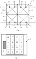
- Figure 2 is a schematic representation of a die 10 according to an embodiment of the present disclosure.
- the die 10 may be a beamforming chip.
- the die 10 is divided into a plurality of unit cells 15.
- Each unit cell 15 may be the same size and shape. It will be appreciated that although Figure 2 shows the die 10 comprising a 4 x 4 array of unit cells, this is not limiting.
- the die 10 may comprise any number of unit cells 15.
- Figure 3 is a close-up of one of the unit cells 15 of the die 10.
- the unit cell 15 may be considered to be divided into four quadrants, a first quadrant 11, a second quadrant 12, a third quadrant 13 and a fourth quadrant 14.
- the lines dividing the unit cell 15 into quadrants may be mathematical constructs, as no physical barrier or division may be present.
- the nearest neighbour quadrants in a unit cell are the quadrants that are immediately adjacent to a given quadrant. For example, for the first quadrant 11 the nearest neighbour quadrants are the second quadrant 12 and the fourth quadrant 14, but not the third quadrant 13.
- each quadrant comprises a receiver terminal 16 and a transmitter terminal 18.
- Each receiver terminal 16 is a coaxial input connection for the receiver channel of an antenna element
- each transmitter terminal 18 is a coaxial output connection for the transmitter channel of an antenna element.
- the receiver terminal 16 is located on a first axis A and the transmitter terminal 18 is located on a second axis B.
- the first axis A is orthogonal to the second axis B.
- the first axis A and the second axis B are diagonal axes.
- the receiver terminal 16 and the transmitter terminal 18 are also aligned along a third axis C of the quadrant, wherein the third axis C intersects the first axis A and the second axis B.
- the third axis C is at an angle of around 45° relative to the first axis A and the second axis B. It will be appreciated that the first axis A, the second axis B and the third axis C are mathematical constructs.
- the location of the receiver terminal 16 and transmitter terminal 18 is not the same in each quadrant 11-14 of the unit cell 15.
- the orientation of the first axis A and the second axis B is not the same in all quadrants of the unit cell 15.
- the orientation of the first axis A and the second axis B in the nearest neighbour quadrants of the unit cell 15 therefore has mirror symmetry.
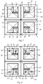
- FIG 4 is a schematic representation of a package 20.
- the package comprises a chip 27 such as an up-down-converter (UDC) and a plurality of unit cells 25.
- UDC up-down-converter
- the package 20 may include an antenna array, or an antenna array may be attached to the package 20.
- each unit cell 15 of the die may be aligned with a unit cell 25 of the package.
- the package 20 may be configured to contain multiple dies 10.
- Each die 10 may comprise a plurality of unit cells 15.
- the package may comprise an array of four dies 10 (e.g. a 2 x 2 array), each die 10 comprising four unit cells 15.
- Each unit cell 25 of the package may be aligned with one of the die unit cells 15.
- Figure 5 shows a close-up of one of the package unit cells 25 in a first configuration.
- the first axis A and second axis B of the die quadrants are shown in Figure 5 to clarify how the package unit cell 25 aligns with the corresponding die unit cell 15.
- the package unit cell 25 may be considered to be divided into four quadrants, a first quadrant 21, a second quadrant 22, a third quadrant 23 and a fourth quadrant 24. It will be appreciated that the lines dividing the unit cell 25 into quadrants may be mathematical constructs, as no physical barrier or division may be present between quadrants.
- Each quadrant 21-24 of the unit cell 25 comprises a pair of feed lines, wherein each pair of feed lines comprises a receiver feed line 26 and a transmitter feed line 28. In each pair, the receiver feed line 26 is orthogonal to the transmitter feed line 28.
- Each receiver feed line 26 is configured to be connected to one of the receiver terminals 16 of the die and each transmitter feed line 28 is configured to be connected to one of the transmitter terminals 18 of the die. As shown in Figure 5 , each feed line is coupled to a connector 29, for example a strip line connector 29. The connectors 29 connect the feed lines 26, 28 to the respective die terminal 16, 18.
- a phased antenna array comprising a plurality of antenna elements 32 is either embedded in, or connected to, the package 20.
- the phase antenna array may be a patch antenna array.
- each antenna element 32 such as a patch antenna, may be aligned with one of the quadrants of the package unit cell 25, and consequently also aligned with one of the quadrants of the die unit cells 15.
- FIG 5 an outline of the antenna elements 32 is illustrated, to show how the antenna array aligns overlays the package unit cells 25.
- Each pair of feed lines 26, 28 is arranged to be connected to a respective one of the antenna elements 32.
- the receiver feed lines 26 drive a receiver channel of the phased antenna array
- the transmitter feed lines 28 drive a transmitter channel of the phased antenna array.
- the feed lines 26, 28 are shown in a first configuration, wherein the receiver feed lines 26 are orientated for horizontal polarization of the antenna array receiver channel and the transmitter feed lines 28 are orientated for vertical polarization of the antenna array transmitter channel.
- receiver feed line 26, transmitter feed line 28, and connectors 29 may have the same dimensions in each quadrant 21-24 of the unit cell 25. This may provide symmetry and reduce irregularities, improving performance of the antenna array.
- Figure 5 is a schematic illustration and so the feed lines 26, 28 and the connectors 29 may not be contained in just a single layer of the package 20.
- FIG 6 shows the package unit cell 25 of Figure 5 overlaying a unit cell 15 of the (or a) die 10 (i.e. when the or each die 10 has been mounted in the package 20).
- each receiver feed line 26 is connected to a respective one of the receiver terminals 16 by a connector 29.
- Each transmitter feed line 28 is connected to a respective one of the transmitter terminals 18 by a connector 29.
- Figure 7 shows a package unit cell 25 in a second configuration.
- the receiver feed lines 26 are orientated for vertical polarization of the antenna array receiver channel and the transmitter feed lines 28 are orientated for horizontal polarization of the antenna array transmitter channel.
- each pair of feed lines 26, 28 has been rotated relative to the first configuration (shown in Figure 5 ).
- the pair of feed lines In the first quadrant 21 and the third quadrant 23 the pair of feed lines have been rotated 90° clockwise about the centre of the quadrant from the first configuration to arrive at the second configuration.
- the pair of feed lines In the second quadrant 22 and the fourth quadrant 24 the pair of feed lines have been rotated 90° anti-clockwise about the centre of the quadrant from the first configuration to arrive at the second configuration.
- the rotation of the feed lines 26, 28 can, in some embodiments, just require changes to the construction of a single layer in the package 20 during the package manufacturing process. This is quite a straightforward, and therefore efficient and relatively inexpensive modification to the package.
- FIG 8 shows the package unit cell 25 of Figure 7 overlaying a unit cell 15 of the (or a) die 10 (i.e. when the or each die 10 has been mounted in the package 20).
- each receiver feed line 26 is connected to a respective one of the receiver terminals 16 by the corresponding connector 29.
- Each transmitter feed line 28 is connected to a respective one of the transmitter terminals 18 by the corresponding connector 29.
- FIG. 6 A comparison between Figures 6 and 8 shows that the die terminals 16, 18 are in the same position, thus the same die(s) can be used when the package feed lines are in the first configuration or in the second configuration. This can improve the cost and efficiency of manufacturing integrated circuits or packages, as the same die can be used for different antenna polarizations.
- the die 10 comprises a phase shifter circuit (not shown).
- the phase shifter circuit may be configured to selectively apply a phase shift to a signal processed by the receiver channel (i.e. the receiver feed lines) and/or the transmitter channel (i.e. the transmitter feed lines) of the antenna array.
- the phase shifter circuit may only be activated in one of the first configuration or the second configuration. For example, in the second configuration as shown in Figure 8 the die 10 may apply a 180° phase shift to signals processed by the transmitter channel.
- Figure 9 shows a first package 20 comprising a plurality of unit cells 25 and a UDC 27 (as shown in Figure 4 ) and a second package 120 comprising a plurality of unit cells 125 and a UDC 127.
- the second package 125 may be identical to the first package 20.
- the first package 20 is mounted adjacent to the second package 120 to form a multi-package module 100.
- the second package 120 may be rotated 180° relative to the first package 20.
- the multi-package module may be referred to as an integrated circuit 100 comprising a first package 20 and a second package 120.
- the antenna array of the first package 20 and the second package 120 may be sub-arrays that together form a larger antenna array.
- the feed lines 26, 28 of the first package 20 and the second package 120 may be in the same configuration.
- both packages may be in the first configuration, or the second configuration.
- FIG 10 shows a schematic illustration of a semiconductor device 50 comprising a 4 x 2 array of integrated circuits 100-800.
- Each integrated circuit 100-800 may comprise a package 20, at least one die 10 and a phased antenna array as described above (not shown). It will be appreciated that the array may be of any size.
- each integrated circuit 100, 300, 500, 700 in the first column of the array may have a first polarization
- each integrated circuit 200, 400, 600, 800 in the second column of the array may have a second polarization.
- each integrated circuit 100, 300, 500, 700 in the first column the pairs of feed lines 26, 28 in the packages may be in the first configuration (as in Figure 5 ), and in each integrated circuit 200, 400, 600, 800 in the second column the pairs of feed lines 26, 28 in the packages may be in the second configuration (as in Figure 7 ), or vice versa. This may increase the capacity of the overall antenna array.
- the plurality of dies 10 in each integrated circuit may be identical.
- each integrated circuit 100-800 may be a multi-package module comprising at least a first and second package, as shown in Figure 9 .
- FIG 11 shows a schematic illustration of another embodiment of a semiconductor device 50.
- the semiconductor device 50 comprises a 2 x 3 array of integrated circuits or multi-pack modules 100-600.
- each integrated circuit 100, 200, 300 in the first row of the array may have a first polarization and each integrated circuit 400, 500, 600 in the second row of the array may have a second polarization.
- each integrated circuit 100, 200, 300 in the first row the pairs of feed lines 26, 28 in the packages may be in the first configuration (as in Figure 5 )
- each integrated circuit 400, 500, 600 in the second row the pairs of feed lines 26, 28 in the packages may be in the second configuration (as in Figure 7 ), or vice versa. This may increase the capacity of the overall antenna array.
- the plurality of dies 10 in each integrated circuit may be identical.
- the present disclosure may reduce irregularities and asymmetry in arrays formed of multiple integrated circuits, for example as shown in Figures 10 and 11 . This is because the same die can be used in the integrated circuits regardless of the polarization required by the antenna array. In addition, allowing the same die to be used in different package configurations reduces costs and improves efficiency of the manufacturing process.
- an integrated circuit comprising a package, a phased antenna array comprising a plurality of antenna elements and a die contained within the package.
- the die comprises a plurality of unit cells, wherein each unit cell is divided into quadrants, and each quadrant comprises a receiver terminal located on a first axis of the quadrant; and a transmitter terminal located on a second axis of the quadrant, wherein the first axis is orthogonal to the second axis, wherein there is mirror symmetry between the nearest neighbour quadrants in the unit cell.
- the package comprises a plurality of pairs of feed lines, each pair of feed lines comprising a receiver feed line and a transmitter feed line, wherein the receiver feed line is connected to one of the receiver terminals and the transmitter feed line is connected to the transmitter terminal in the same quadrant of the die, wherein the receiver feed line is orthogonal to the transmitter feed line.
- Each antenna element of the phased antenna array is coupled to a respective pair of feed lines to drive a receiver channel and a transmitter channel of the phased antenna array.
Landscapes
- Engineering & Computer Science (AREA)
- Microelectronics & Electronic Packaging (AREA)
- Variable-Direction Aerials And Aerial Arrays (AREA)
Abstract
Description
- The present specification relates to integrated circuits comprising a package, a phased antenna array and a die, wherein the same die can be used with different antenna polarizations.
- For beam-forming of mmWave signals, the antenna array required can become too large to be covered by one die. Therefore, it is known for a package to contain multiple dies to control an antenna array. It is also known to place two or more packages close together on a printed circuit board, each package comprising an antenna sub-array, to form a larger antenna array. To increase the capacity some of the antenna sub-arrays may operate in a horizontal polarization, and other antenna sub-arrays may operate in a vertical polarization.
- Typically, antenna arrays or sub-arrays operating in a vertical polarization require a different die to the antenna arrays or sub-arrays operating in a horizontal polarization. This is because the layout of the connections in the package, such as the antenna feed lines and transmission lines, have a different layout depending on the antenna polarization, which then requires a different layout for the die terminals.
- Any asymmetry or irregularities between dies or between packages in the array can result in RF loses and reduced performance of the array. In addition, differences between the dies or packages required for different polarizations increases manufacturing time and costs.
- Aspects of the present disclosure are set out in the accompanying independent and dependent claims. Combinations of features from the dependent claims may be combined with features of the independent claims as appropriate and not merely as explicitly set out in the claims.
- According to an aspect of the present disclosure, there is provided an integrated circuit comprising a package, a phased antenna array comprising a plurality of antenna elements, and a die contained within the package. The die comprises a plurality of unit cells, wherein each unit cell is divided into quadrants, and each quadrant comprises a receiver terminal located on a first axis of the quadrant, and a transmitter terminal located on a second axis of the quadrant, wherein the first axis is orthogonal to the second axis, and wherein the location of the receiver terminal and the transmitter terminal in the nearest neighbour quadrants in a given unit cell has mirror symmetry. The package comprises a plurality of pairs of feed lines, each pair of feed lines comprising a receiver feed line and a transmitter feed line, wherein the receiver feed line is connected to one of the receiver terminals and the transmitter feed line is connected to the transmitter terminal in the same quadrant of the die, wherein the receiver feed line is orthogonal to the transmitter feed line. Each antenna element of the phased antenna array is coupled to a respective pair of feed lines to drive a receiver channel and a transmitter channel.
- It will be appreciated that the quadrants of each unit cell of the die could be any shape. They are not limited to being square or rectangular.
- The nearest neighbour quadrants to a given quadrant are the quadrants that are adjacent to the quadrant, not including those quadrants that are diagonally adjacent.
- The first axis and the second axis in the nearest neighbour quadrants in a given unit cell may have mirror symmetry.
- The term 'package' may be used interchangeably with 'integrated circuit package' throughout this disclosure.
- The phased antenna array may be contained within the package, thus the package may be an antenna-in-package (AiP) package or a launcher-in-package (LiP) package. In other embodiments, the phased antenna array may be provided externally to the package. The package may be an antenna-on-package (AoP) package, or the antenna array may be attached to the package as a package-on-package (PoP).
- Optionally, the phased antenna array may comprise a patch antenna array, such that each antenna element may comprise a patch antenna. However, any type of phased antenna array may be used.
- Optionally, each antenna element is aligned with a respective one of the quadrants of the die.
- Each receiver feed line may be connected to the respective receiver terminal on the die by a strip line connection, or other electrical connection. Each transmitter feed line may be connected to the respective transmitter terminal on the die by a strip line connection, or other electrical connection.
- The plurality of pairs of feed lines may have a first configuration and a second configuration. The configuration of the feed lines may be fixed during manufacture of the package, such that the feed lines are not reconfigurable during use of the integrated circuit. Optionally, in the first configuration, the receiver channel may have a horizontal polarization and the transmitter channel may have a vertical polarization. In the second configuration, the receiver channel may have a vertical polarization and the transmitter channel may have a horizontal polarization.
- Thus, the die terminals remain in the same fixed position regardless of whether the antenna feed lines in the package are in the first configuration or the second configuration.
- Optionally, in the first configuration each pair of feed lines is rotated relative to the second configuration. In some embodiments each pair of feed lines may be rotated by 90° between the first and second configurations.
- In the first configuration, each receiver feed line may be rotated 90° about the respective receiver die terminal relative to the position of the receiver feed line in the second configuration. In the first configuration, each transmitter feed line may be rotated 90° about the respective transmitter die terminal relative to the position of the transmitter feed line in the second configuration.
- Optionally, in the first configuration each receiver feed line may have a horizontal orientation and each transmitter feed line may have a vertical orientation. Optionally, in the second configuration each receiver feed line may have a vertical orientation and each transmitter feed line may have a horizontal orientation.
- Optionally, the package comprises a plurality of unit cells and each unit cell is divided into quadrants. Each quadrant may comprise one of the pairs of feed lines, and each unit cell of the package may overlay a respective unit cell of the die.
- The orientation of the pair of feed lines in the nearest neighbour quadrants in each unit cell of the package may have mirror symmetry.
- Each pair of feed lines may be rotated about a centre of the quadrant between the first configuration and the second configuration.
- In the first configuration, each pair of feed lines may be rotated 90° in the opposite direction to the nearest neighbour quadrant in the unit cell of the package, relative to the second configuration.
- For example, the pair of feed lines in the first quadrant and the third quadrant of a given unit cell of the package may be rotated 90° anti-clockwise in the second configuration relative to the first configuration. The pair of feed lines in the second quadrant and the fourth quadrant of the same unit cell may be rotated 90° clockwise in the second configuration relative to the first configuration.
- Optionally, the first axis and the second axis are each axes of symmetry of the die quadrant. Optionally, the first axis and the second axis are each diagonal axes.
- Optionally, in each quadrant of the die the receiver terminal and the transmitter terminal are aligned along a third axis. In some embodiments, the third axis may be at an angle of 45° relative to the first axis and the second axis.
- Each unit cell of the die may comprise a first quadrant, a second quadrant, a third quadrant and a fourth quadrant. The layout (or numbering) of the quadrants follows standard mathematical convention, as shown in
Figure 1 of the drawings. In each unit cell there may be mirror symmetry between: the first quadrant and the second quadrant; the second quadrant and the third quadrant; the third quadrant and the fourth quadrant; and the fourth quadrant and the first quadrant. - Optionally, the die is configured to apply a phase shift, such as a 180 degree phase shift, to a signal processed by the receiver channel and/or the transmitter channel of the antenna array. The die may comprise a phase shifter circuit.
- In some embodiments, a plurality of dies may be contained or mounted in the package. Each die comprises at least one unit cell, wherein each unit cell is divided into quadrants, and each quadrant comprises a receiver terminal located on a first axis of the quadrant, and a transmitter terminal located on a second axis of the quadrant, wherein the first axis is orthogonal to the second axis, and wherein the location of the receiver terminal and the transmitter terminal in the nearest neighbour quadrants in the unit cell has mirror symmetry.
- Optionally, the plurality of dies may be identical. Each of the dies may be as described above in any embodiment of the disclosure.
- Optionally, in each pair of feed lines the receiver feed line has the same dimensions as the transmitter feed line.
- Optionally, each receiver feed line has the same dimensions as each transmitter feed line.
- Optionally, the integrated circuit may comprise a plurality of packages, wherein the packages are as described in any embodiment of the disclosure.
- In a second aspect, the present disclosure provides a semiconductor device, comprising a plurality of integrated circuits arranged to form an array, wherein each integrated circuit is as defined in any embodiment or example of the first aspect of the invention.
- Alternatively, each integrated circuit may be referred to as a multi-package module, wherein each multi-package module comprises a plurality of packages.
- The array of integrated circuits may comprise a plurality of columns and a plurality of rows.
- In some embodiments, in each integrated circuit in a first column of the array, each pair of antenna feed lines may be in the first configuration, such that the antenna arrays have a first polarization. In each integrated circuit in a second column of the array adjacent to the first column, each pair of antenna feed lines may be in the second configuration, such that the antenna arrays have a second polarization.
- In some embodiments, in each integrated circuit in a first row of the array each pair of antenna feed lines may be in the first configuration, such that the antenna arrays have a first polarization. In each integrated circuit in a second row of the array adjacent to the first row, each pair of antenna feed lines may be in the second configuration, such that the antenna arrays have a second polarization.
- In a third aspect, the present disclosure provides a method of manufacturing an integrated circuit. The method comprises providing a die, wherein the die comprises a plurality of unit cells, wherein each unit cell is divided into quadrants, and each quadrant comprises a receiver terminal located on a first axis of the quadrant, and a transmitter terminal located on a second axis of the quadrant, wherein the first axis is orthogonal to the second axis, wherein the location of the receiver terminal and the transmitter terminal in the nearest neighbour quadrants in the unit cell has mirror symmetry. The method further includes providing a phased antenna array comprising a plurality of antenna elements, and assembling a package, wherein assembling the package comprises: encasing the die in the package, providing a plurality of pairs of feed lines, each pair of feed lines comprising a receiver feed line and a transmitter feed line, connecting the receiver feed line to one of the receiver terminals and connecting the transmitter feed line to the transmitter terminal in the same quadrant of the die, wherein the receiver feed line is orthogonal to the transmitter feed line; and coupling each antenna element of the phased antenna array to a respective pair of feed lines to drive a receiver channel and a transmitter channel.
- Optionally, the method may include providing a plurality of dies and encasing the plurality of dies in the package, wherein each of the dies are as described above. The plurality of dies may be identical.
- Optionally, the method may be a method of manufacturing an integrated circuit according to any embodiment of the present disclosure.
- In a further aspect, the present disclosure may provide a semiconductor die configured for beamforming a phased antenna array, the die comprising a plurality of unit cells, wherein each unit cell is divided into quadrants, and each quadrant comprises: a receiver terminal located on a first axis of the quadrant; and a transmitter terminal located on a second axis of the quadrant, wherein the first axis is orthogonal to the second axis, wherein the receiver terminal and the transmitter terminal are configured to be connected to an antenna element of a phased antenna array; and wherein the location of the receiver terminal and transmitter terminal in adjacent quadrants of the unit cell has mirror symmetry.
- The term 'nearest neighbour' may equivalently be used instead of 'adjacent'.
- Optionally, the first axis and the second axis are each axes of symmetry of the die quadrant. Optionally, the first axis and the second axis are each diagonal axes.
- Optionally, in each quadrant of the die the receiver terminal and the transmitter terminal are aligned along a third axis. In some embodiments, the third axis may be at an angle of 45° relative to the first axis and the second axis.
- Each unit cell of the die may comprise a first quadrant, a second quadrant, a third quadrant and a fourth quadrant. The layout (or numbering) of the quadrants follows standard mathematical convention, as shown in
Figure 1 of the drawings. In each unit cell there may be mirror symmetry between: the first quadrant and the second quadrant; the second quadrant and the third quadrant; the third quadrant and the fourth quadrant; and the fourth quadrant and the first quadrant. - Optionally, the die is configured to apply a phase shift, such as a 180 degree phase shift, to a signal processed by the receiver channel and/or the transmitter channel of the antenna array. The die may comprise a phase shifter circuit.
- It will be appreciated that the die may be as defined in any above example or embodiment of the disclosure.
- Illustrative embodiments of this disclosure will be described hereinafter, by way of example only, with reference to the accompanying drawings in which like reference signs relate to like elements and in which:
-
Figure 1 - is a prior art diagram showing a circle and a square divided into quadrants, illustrating the standard convention for numbering quadrants; -
Figure 2 - shows a schematic illustration of a die divided into a plurality of unit cells according to an embodiment of the present disclosure; -
Figure 3 - shows a schematic illustration of one of the unit cells of the die inFigure 2 ; -
Figure 4 - shows a schematic illustration of a package comprising a plurality of unit cells according to an embodiment of the present disclosure; -
Figure 5 - shows one of the unit cells of the package inFigure 4 in a first configuration; -
Figure 6 - shows the package unit cell ofFigure 5 overlaying the die unit cell ofFigure 3 ; -
Figure 7 - shows one of the unit cells of the package inFigure 4 in a second configuration; -
Figure 8 - shows the package unit cell ofFigure 7 overlaying the die unit cell ofFigure 3 ; -
Figure 9 - is a schematic illustration of a first package and a second package according to an embodiment of the present disclosure; -
Figure 10 - is a schematic illustration of a 4 x 2 array of integrated circuits according to an embodiment of the present disclosure; and -
Figure 11 - is a schematic illustration of a 2 x 3 array of integrated circuits according to an embodiment of the present disclosure. - Embodiments of this disclosure are described in the following with reference to the accompanying drawings. It will be appreciated that the drawings are schematic illustrations and are not drawn to scale.
-
Figure 1 is a diagram showing a circle and a square divided into quadrants by two orthogonal axes. Thus, as shown, quadrants do not have to be square in shape. This diagram is provided to show the standard numbering convention for quadrants. By convention, the top-right quadrant is the first quadrant, 1, the top-left quadrant is the second quadrant, 2, the bottom-left quadrant is the third quadrant, 3, and the bottom-right quadrant is the fourth quadrant, 4. This numbering convention will be adhered to throughout the present disclosure. -
Figure 2 is a schematic representation of a die 10 according to an embodiment of the present disclosure. The die 10 may be a beamforming chip. Thedie 10 is divided into a plurality ofunit cells 15. Eachunit cell 15 may be the same size and shape. It will be appreciated that althoughFigure 2 shows the die 10 comprising a 4 x 4 array of unit cells, this is not limiting. The die 10 may comprise any number ofunit cells 15. -
Figure 3 is a close-up of one of theunit cells 15 of thedie 10. Theunit cell 15 may be considered to be divided into four quadrants, afirst quadrant 11, asecond quadrant 12, athird quadrant 13 and afourth quadrant 14. It will be appreciated that the lines dividing theunit cell 15 into quadrants may be mathematical constructs, as no physical barrier or division may be present. The nearest neighbour quadrants in a unit cell are the quadrants that are immediately adjacent to a given quadrant. For example, for thefirst quadrant 11 the nearest neighbour quadrants are thesecond quadrant 12 and thefourth quadrant 14, but not thethird quadrant 13. - As shown in
Figure 3 , each quadrant comprises areceiver terminal 16 and atransmitter terminal 18. Eachreceiver terminal 16 is a coaxial input connection for the receiver channel of an antenna element, and eachtransmitter terminal 18 is a coaxial output connection for the transmitter channel of an antenna element. - In each quadrant 11-14, the
receiver terminal 16 is located on a first axis A and thetransmitter terminal 18 is located on a second axis B. The first axis A is orthogonal to the second axis B. In this embodiment, the first axis A and the second axis B are diagonal axes. In each quadrant 11-14, thereceiver terminal 16 and thetransmitter terminal 18 are also aligned along a third axis C of the quadrant, wherein the third axis C intersects the first axis A and the second axis B. In this embodiment, the third axis C is at an angle of around 45° relative to the first axis A and the second axis B. It will be appreciated that the first axis A, the second axis B and the third axis C are mathematical constructs. - As shown in
Figure 3 , the location of thereceiver terminal 16 andtransmitter terminal 18 is not the same in each quadrant 11-14 of theunit cell 15. In other words, the orientation of the first axis A and the second axis B is not the same in all quadrants of theunit cell 15. - There is mirror symmetry between the position of the
receiver terminal 16 and thetransmitter terminal 18 in thefirst quadrant 11 and the nearest neighbour quadrants 12 and 14 of theunit cell 15. There is mirror symmetry between the position of thereceiver terminal 16 and thetransmitter terminal 18 in thesecond quadrant 12 and the nearest neighbour quadrants 13 and 11 of theunit cell 15. There is mirror symmetry between the position of thereceiver terminal 16 and thetransmitter terminal 18 in thethird quadrant 13 and the nearest neighbour quadrants 12 and 14 of theunit cell 15. There is mirror symmetry between the position of thereceiver terminal 16 and thetransmitter terminal 18 in thefourth quadrant 14 and the nearest neighbour quadrants 13 and 11 of theunit cell 15. - The orientation of the first axis A and the second axis B in the nearest neighbour quadrants of the
unit cell 15 therefore has mirror symmetry. -
Figure 4 is a schematic representation of apackage 20. In this embodiment the package comprises achip 27 such as an up-down-converter (UDC) and a plurality ofunit cells 25. To form an integrated circuit, at least one die 10 is mounted in thepackage 20. Thepackage 20 may include an antenna array, or an antenna array may be attached to thepackage 20. When the die 10 is mounted in thepackage 20 eachunit cell 15 of the die may be aligned with aunit cell 25 of the package. Alternatively, thepackage 20 may be configured to contain multiple dies 10. Each die 10 may comprise a plurality ofunit cells 15. For example, referring toFigure 2 , instead of asingle die 10 comprising sixteen unit cells, the package may comprise an array of four dies 10 (e.g. a 2 x 2 array), each die 10 comprising fourunit cells 15. Eachunit cell 25 of the package may be aligned with one of thedie unit cells 15. -
Figure 5 shows a close-up of one of thepackage unit cells 25 in a first configuration. The first axis A and second axis B of the die quadrants are shown inFigure 5 to clarify how thepackage unit cell 25 aligns with the correspondingdie unit cell 15. Thepackage unit cell 25 may be considered to be divided into four quadrants, afirst quadrant 21, asecond quadrant 22, athird quadrant 23 and afourth quadrant 24. It will be appreciated that the lines dividing theunit cell 25 into quadrants may be mathematical constructs, as no physical barrier or division may be present between quadrants. - Each quadrant 21-24 of the
unit cell 25 comprises a pair of feed lines, wherein each pair of feed lines comprises areceiver feed line 26 and atransmitter feed line 28. In each pair, thereceiver feed line 26 is orthogonal to thetransmitter feed line 28. - Each
receiver feed line 26 is configured to be connected to one of thereceiver terminals 16 of the die and eachtransmitter feed line 28 is configured to be connected to one of thetransmitter terminals 18 of the die. As shown inFigure 5 , each feed line is coupled to aconnector 29, for example astrip line connector 29. Theconnectors 29 connect the feed lines 26, 28 to therespective die terminal - In use, a phased antenna array comprising a plurality of
antenna elements 32 is either embedded in, or connected to, thepackage 20. The phase antenna array may be a patch antenna array. When the integrated circuit is fully assembled, eachantenna element 32, such as a patch antenna, may be aligned with one of the quadrants of thepackage unit cell 25, and consequently also aligned with one of the quadrants of thedie unit cells 15. InFigure 5 , an outline of theantenna elements 32 is illustrated, to show how the antenna array aligns overlays thepackage unit cells 25. Each pair offeed lines antenna elements 32. Thus, thereceiver feed lines 26 drive a receiver channel of the phased antenna array and thetransmitter feed lines 28 drive a transmitter channel of the phased antenna array. - In
Figure 5 the feed lines 26, 28 are shown in a first configuration, wherein thereceiver feed lines 26 are orientated for horizontal polarization of the antenna array receiver channel and thetransmitter feed lines 28 are orientated for vertical polarization of the antenna array transmitter channel. - There is mirror symmetry between the orientation of the pair of
feed lines unit cell 25. Thus, as shown inFigure 5 , there is mirror symmetry between: thefirst quadrant 21 and thesecond quadrant 22; thesecond quadrant 22 and thethird quadrant 23; thethird quadrant 23 and thefourth quadrant 24; and thefourth quadrant 24 and thefirst quadrant 21. - It may be preferable for the
receiver feed line 26,transmitter feed line 28, andconnectors 29 to have the same dimensions in each quadrant 21-24 of theunit cell 25. This may provide symmetry and reduce irregularities, improving performance of the antenna array. - It will be appreciated that
Figure 5 is a schematic illustration and so the feed lines 26, 28 and theconnectors 29 may not be contained in just a single layer of thepackage 20. -
Figure 6 shows thepackage unit cell 25 ofFigure 5 overlaying aunit cell 15 of the (or a) die 10 (i.e. when the or each die 10 has been mounted in the package 20). As shown, eachreceiver feed line 26 is connected to a respective one of thereceiver terminals 16 by aconnector 29. Eachtransmitter feed line 28 is connected to a respective one of thetransmitter terminals 18 by aconnector 29. -
Figure 7 shows apackage unit cell 25 in a second configuration. In the second configuration thereceiver feed lines 26 are orientated for vertical polarization of the antenna array receiver channel and thetransmitter feed lines 28 are orientated for horizontal polarization of the antenna array transmitter channel. - In the second configuration, the orientation of each pair of
feed lines Figure 5 ). In thefirst quadrant 21 and thethird quadrant 23 the pair of feed lines have been rotated 90° clockwise about the centre of the quadrant from the first configuration to arrive at the second configuration. In thesecond quadrant 22 and thefourth quadrant 24 the pair of feed lines have been rotated 90° anti-clockwise about the centre of the quadrant from the first configuration to arrive at the second configuration. However, there is still mirror symmetry between the nearest neighbour quadrants in the second configuration, as there is in the first configuration. - The rotation of the feed lines 26, 28 can, in some embodiments, just require changes to the construction of a single layer in the
package 20 during the package manufacturing process. This is quite a straightforward, and therefore efficient and relatively inexpensive modification to the package. -
Figure 8 shows thepackage unit cell 25 ofFigure 7 overlaying aunit cell 15 of the (or a) die 10 (i.e. when the or each die 10 has been mounted in the package 20). As shown, eachreceiver feed line 26 is connected to a respective one of thereceiver terminals 16 by the correspondingconnector 29. Eachtransmitter feed line 28 is connected to a respective one of thetransmitter terminals 18 by the correspondingconnector 29. - A comparison between
Figures 6 and8 shows that thedie terminals - Optionally, the
die 10 comprises a phase shifter circuit (not shown). The phase shifter circuit may be configured to selectively apply a phase shift to a signal processed by the receiver channel (i.e. the receiver feed lines) and/or the transmitter channel (i.e. the transmitter feed lines) of the antenna array. In some embodiments, the phase shifter circuit may only be activated in one of the first configuration or the second configuration. For example, in the second configuration as shown inFigure 8 thedie 10 may apply a 180° phase shift to signals processed by the transmitter channel. -
Figure 9 shows afirst package 20 comprising a plurality ofunit cells 25 and a UDC 27 (as shown inFigure 4 ) and asecond package 120 comprising a plurality ofunit cells 125 and aUDC 127. Thesecond package 125 may be identical to thefirst package 20. Thefirst package 20 is mounted adjacent to thesecond package 120 to form amulti-package module 100. Thesecond package 120 may be rotated 180° relative to thefirst package 20. Equivalently, the multi-package module may be referred to as anintegrated circuit 100 comprising afirst package 20 and asecond package 120. Thus, the antenna array of thefirst package 20 and the second package 120 (not shown) may be sub-arrays that together form a larger antenna array. - Methods of forming a
multi-package module 100 from at least a first package and a second package are described in detail in European patent application no.EP21157067.6 - The feed lines 26, 28 of the
first package 20 and thesecond package 120 may be in the same configuration. For example, both packages may be in the first configuration, or the second configuration. -
Figure 10 shows a schematic illustration of asemiconductor device 50 comprising a 4 x 2 array of integrated circuits 100-800. Each integrated circuit 100-800 may comprise apackage 20, at least onedie 10 and a phased antenna array as described above (not shown). It will be appreciated that the array may be of any size. In some embodiments, eachintegrated circuit integrated circuit integrated circuit feed lines Figure 5 ), and in eachintegrated circuit feed lines Figure 7 ), or vice versa. This may increase the capacity of the overall antenna array. The plurality of dies 10 in each integrated circuit may be identical. - Alternatively, each integrated circuit 100-800 may be a multi-package module comprising at least a first and second package, as shown in
Figure 9 . -
Figure 11 shows a schematic illustration of another embodiment of asemiconductor device 50. Thesemiconductor device 50 comprises a 2 x 3 array of integrated circuits or multi-pack modules 100-600. - In some embodiments, each
integrated circuit integrated circuit integrated circuit feed lines Figure 5 ), and in eachintegrated circuit feed lines Figure 7 ), or vice versa. This may increase the capacity of the overall antenna array. The plurality of dies 10 in each integrated circuit may be identical. - The present disclosure may reduce irregularities and asymmetry in arrays formed of multiple integrated circuits, for example as shown in
Figures 10 and11 . This is because the same die can be used in the integrated circuits regardless of the polarization required by the antenna array. In addition, allowing the same die to be used in different package configurations reduces costs and improves efficiency of the manufacturing process. - Accordingly, there has been described an integrated circuit comprising a package, a phased antenna array comprising a plurality of antenna elements and a die contained within the package. The die comprises a plurality of unit cells, wherein each unit cell is divided into quadrants, and each quadrant comprises a receiver terminal located on a first axis of the quadrant; and a transmitter terminal located on a second axis of the quadrant, wherein the first axis is orthogonal to the second axis, wherein there is mirror symmetry between the nearest neighbour quadrants in the unit cell. The package comprises a plurality of pairs of feed lines, each pair of feed lines comprising a receiver feed line and a transmitter feed line, wherein the receiver feed line is connected to one of the receiver terminals and the transmitter feed line is connected to the transmitter terminal in the same quadrant of the die, wherein the receiver feed line is orthogonal to the transmitter feed line. Each antenna element of the phased antenna array is coupled to a respective pair of feed lines to drive a receiver channel and a transmitter channel of the phased antenna array.
- Although particular embodiments of this disclosure have been described, it will be appreciated that many modifications/additions and/or substitutions may be made within the scope of the claims.
Claims (15)
- An integrated circuit comprising:a package;a phased antenna array comprising a plurality of antenna elements; anda die contained within the package;wherein the die comprises a plurality of unit cells, wherein each unit cell is divided into quadrants, and each quadrant comprises:a receiver terminal located on a first axis of the quadrant; anda transmitter terminal located on a second axis of the quadrant, wherein the first axis is orthogonal to the second axis,wherein there is mirror symmetry between the nearest neighbour quadrants in the unit cell;wherein the package comprises:a plurality of pairs of feed lines, each pair of feed lines comprising a receiver feed line and a transmitter feed line, wherein the receiver feed line is connected to one of the receiver terminals and the transmitter feed line is connected to the transmitter terminal in the same quadrant of the die, wherein the receiver feed line is orthogonal to the transmitter feed line; andwherein each antenna element of the phased antenna array is coupled to a respective pair of feed lines to drive a receiver channel and a transmitter channel.
- The integrated circuit of claim 1, wherein the plurality of pairs of feed lines have a first configuration and second configuration, wherein:in the first configuration the receiver channel has a horizontal polarization and the transmitter channel has a vertical polarization; andin the second configuration the receiver channel has a vertical polarization and the transmitter channel has a horizontal polarization.
- The integrated circuit of claim 2, wherein in the first configuration each pair of feed lines is rotated 90° relative to the second configuration.
- The integrated circuit of claim 2 or claim 3, wherein the package comprises a plurality of unit cells and each unit cell is divided into quadrants, wherein:each quadrant comprises one of the pairs of feed lines;each unit cell of the package overlays a respective unit cell of the die; andin the first configuration each pair of feed lines is rotated 90° in the opposite direction to the nearest neighbour quadrants in the unit cell, relative to the second configuration.
- The integrated circuit of any of claims 1 to 3, wherein the package comprises a plurality of unit cells and each unit cell is divided into quadrants, wherein:each quadrant comprises one of the pairs of feed lines; andeach unit cell of the package overlays a respective unit cell of the die.
- The integrated circuit of claim 5, wherein the orientation of the pair of feed lines in the nearest neighbour quadrants in each unit cell of the package has mirror symmetry.
- The integrated circuit of any preceding claim, wherein the die comprises a phase shifter circuit, wherein the phase shifter circuit is configured to apply a 180 degree phase shift to a signal processed the receiver channel and/or the transmitter channel.
- The integrated circuit of any preceding claim, further comprising a plurality of dies contained in the package, wherein each die comprises at least one unit cell, wherein each unit cell is divided into quadrants, and each quadrant comprises:a receiver terminal located on a first axis of the quadrant; anda transmitter terminal located on a second axis of the quadrant, wherein the first axis is orthogonal to the second axis,wherein the location of the receiver terminal and the transmitter terminal in the nearest neighbour quadrants in the unit cell has mirror symmetry.
- The integrated circuit of claim 8, wherein the plurality of dies are identical.
- The integrated circuit of any preceding claim, wherein the first axis and the second axis are each axes of symmetry of the quadrant, and/or wherein the first axis and the second axis are each diagonal axes.
- The integrated circuit of any preceding claim, wherein in each quadrant of the, or each, die the receiver terminal and the transmitter terminal are aligned along a third axis.
- The integrated circuit of any preceding claim, wherein each unit cell of the, or each, die comprises a first quadrant, a second quadrant, a third quadrant and a fourth quadrant, wherein in each unit cell there is mirror symmetry between:the first quadrant and the second quadrant;the second quadrant and the third quadrant;the third quadrant and the fourth quadrant; andthe fourth quadrant and the first quadrant.
- The integrated circuit of any preceding claim, wherein in each pair of feed lines the receiver feed line has the same dimensions as the transmitter feed line, or wherein each receiver feed line has the same dimensions as each transmitter feed line.
- A semiconductor device, comprising:
a plurality of integrated circuits arranged to form an array, wherein each integrated circuit is as defined in any preceding claim. - A method of manufacturing an integrated circuit, comprising:providing a die, wherein the die comprises a plurality of unit cells, wherein each unit cell is divided into quadrants, and each quadrant comprises:a receiver terminal located on a first axis of the quadrant; anda transmitter terminal located on a second axis of the quadrant, wherein the first axis is orthogonal to the second axis,wherein the location of the receiver terminal and the transmitter terminal in the nearest neighbour quadrants in the unit cell has mirror symmetry;providing a phased antenna array comprising a plurality of antenna elements; andassembling a package, wherein assembling the package comprises:encasing the die in the package;providing a plurality of pairs of feed lines, each pair of feed lines comprising a receiver feed line and a transmitter feed line,connecting the receiver feed line to one of the receiver terminals and connecting the transmitter feed line to the transmitter terminal in the same quadrant of the die, wherein the receiver feed line is orthogonal to the transmitter feed line; andcoupling each antenna element of the phased antenna array to a respective pair of feed lines to drive a receiver channel and a transmitter channel.
Priority Applications (3)
| Application Number | Priority Date | Filing Date | Title |
|---|---|---|---|
| EP21165473.6A EP4068505B1 (en) | 2021-03-29 | 2021-03-29 | Single die design for different polarizations |
| CN202210139573.7A CN115149281A (en) | 2021-03-29 | 2022-02-15 | Single die design for different polarizations |
| US17/651,832 US12212074B2 (en) | 2021-03-29 | 2022-02-21 | Single die design for different polarizations |
Applications Claiming Priority (1)
| Application Number | Priority Date | Filing Date | Title |
|---|---|---|---|
| EP21165473.6A EP4068505B1 (en) | 2021-03-29 | 2021-03-29 | Single die design for different polarizations |
Publications (2)
| Publication Number | Publication Date |
|---|---|
| EP4068505A1 true EP4068505A1 (en) | 2022-10-05 |
| EP4068505B1 EP4068505B1 (en) | 2024-11-20 |
Family
ID=75252559
Family Applications (1)
| Application Number | Title | Priority Date | Filing Date |
|---|---|---|---|
| EP21165473.6A Active EP4068505B1 (en) | 2021-03-29 | 2021-03-29 | Single die design for different polarizations |
Country Status (3)
| Country | Link |
|---|---|
| US (1) | US12212074B2 (en) |
| EP (1) | EP4068505B1 (en) |
| CN (1) | CN115149281A (en) |
Families Citing this family (1)
| Publication number | Priority date | Publication date | Assignee | Title |
|---|---|---|---|---|
| EP4044227B1 (en) | 2021-02-15 | 2025-07-30 | Nxp B.V. | Uniform multi-package antenna array |
Citations (3)
| Publication number | Priority date | Publication date | Assignee | Title |
|---|---|---|---|---|
| US20160197404A1 (en) * | 2015-01-06 | 2016-07-07 | Kabushiki Kaisha Toshiba | Dual-polarized antenna |
| CN107342458A (en) * | 2017-07-02 | 2017-11-10 | 中国航空工业集团公司雷华电子技术研究所 | A kind of corner-fed formula wide-band high-isolation dual-polarized antenna |
| US20190260138A1 (en) * | 2018-02-21 | 2019-08-22 | International Business Machines Corporation | Scalable phased array package |
Family Cites Families (8)
| Publication number | Priority date | Publication date | Assignee | Title |
|---|---|---|---|---|
| CN205900791U (en) * | 2016-06-21 | 2017-01-18 | 珠海纳睿达科技有限公司 | Planar phased array of low secondary lobe is listed as antenna |
| DE102016112581A1 (en) * | 2016-07-08 | 2018-01-11 | Lisa Dräxlmaier GmbH | Phased array antenna |
| US11171418B2 (en) * | 2017-09-18 | 2021-11-09 | Integrated Device Technology, Inc. | Method to utilize bias current control in vertical or horizontal channels for polarization rotation with less power consumption |
| US11063344B2 (en) * | 2018-02-20 | 2021-07-13 | Samsung Electronics Co., Ltd. | High gain and large bandwidth antenna incorporating a built-in differential feeding scheme |
| US10784563B2 (en) * | 2018-02-21 | 2020-09-22 | International Business Machines Corporation | Scalable phased array package |
| CN108417971B (en) * | 2018-03-26 | 2024-06-21 | 广东纳睿雷达科技股份有限公司 | Dual polarized antenna array and dual polarized phased array antenna |
| US11108165B2 (en) * | 2018-08-17 | 2021-08-31 | The Regents Of The University Of Michigan | Radio frequency front end for full duplex wireless communications |
| EP4044366B1 (en) * | 2021-02-12 | 2023-10-25 | Sivers Wireless AB | An integrated circuit package comprising a crossed dipole antenna |
-
2021
- 2021-03-29 EP EP21165473.6A patent/EP4068505B1/en active Active
-
2022
- 2022-02-15 CN CN202210139573.7A patent/CN115149281A/en active Pending
- 2022-02-21 US US17/651,832 patent/US12212074B2/en active Active
Patent Citations (3)
| Publication number | Priority date | Publication date | Assignee | Title |
|---|---|---|---|---|
| US20160197404A1 (en) * | 2015-01-06 | 2016-07-07 | Kabushiki Kaisha Toshiba | Dual-polarized antenna |
| CN107342458A (en) * | 2017-07-02 | 2017-11-10 | 中国航空工业集团公司雷华电子技术研究所 | A kind of corner-fed formula wide-band high-isolation dual-polarized antenna |
| US20190260138A1 (en) * | 2018-02-21 | 2019-08-22 | International Business Machines Corporation | Scalable phased array package |
Also Published As
| Publication number | Publication date |
|---|---|
| US20220311137A1 (en) | 2022-09-29 |
| EP4068505B1 (en) | 2024-11-20 |
| US12212074B2 (en) | 2025-01-28 |
| CN115149281A (en) | 2022-10-04 |
Similar Documents
| Publication | Publication Date | Title |
|---|---|---|
| US6366238B1 (en) | Phased array beamformer module driving two elements | |
| US9013361B1 (en) | Interlocking subarray configurations | |
| KR101112726B1 (en) | Mobile communication base station antenna | |
| US6686885B1 (en) | Phased array antenna for space based radar | |
| US5434575A (en) | Phased array antenna system using polarization phase shifting | |
| US7245938B2 (en) | Wireless antenna traffic matrix | |
| EP0523422A1 (en) | Directional scanning circular phased array antenna | |
| EP0523409A1 (en) | Electronically reconfigurable antenna | |
| US20070210959A1 (en) | Multi-beam tile array module for phased array systems | |
| WO2013038276A1 (en) | Phased-array transceiver | |
| US4761653A (en) | Microstrip antenna | |
| US20180138592A1 (en) | Multi-beam antenna arrangement | |
| US12562501B2 (en) | Dual-polarization antenna | |
| US12212074B2 (en) | Single die design for different polarizations | |
| EP3400630B1 (en) | Reconfigurable antennas and methods of operating the same | |
| CN113871900B (en) | A two-dimensional MIMO array antenna with high angular resolution and array formation method thereof | |
| US20190131707A1 (en) | Antenna array with abfn circuitry | |
| US11929555B2 (en) | Circular polarization array antenna device | |
| CN212323206U (en) | Base station antenna | |
| US6670931B2 (en) | Antenna having cross polarization improvement using rotated antenna elements | |
| CN112134033A (en) | Hybrid antenna | |
| US11909119B2 (en) | Circular polarization array antenna device | |
| WO2021262345A1 (en) | Base station antenna | |
| US20260031530A1 (en) | Array antenna for reducing grating lobe and cross polarization leakage | |
| CN115020980B (en) | Millimeter wave antenna module and preparation method thereof |
Legal Events
| Date | Code | Title | Description |
|---|---|---|---|
| PUAI | Public reference made under article 153(3) epc to a published international application that has entered the european phase |
Free format text: ORIGINAL CODE: 0009012 |
|
| STAA | Information on the status of an ep patent application or granted ep patent |
Free format text: STATUS: THE APPLICATION HAS BEEN PUBLISHED |
|
| AK | Designated contracting states |
Kind code of ref document: A1 Designated state(s): AL AT BE BG CH CY CZ DE DK EE ES FI FR GB GR HR HU IE IS IT LI LT LU LV MC MK MT NL NO PL PT RO RS SE SI SK SM TR |
|
| STAA | Information on the status of an ep patent application or granted ep patent |
Free format text: STATUS: REQUEST FOR EXAMINATION WAS MADE |
|
| 17P | Request for examination filed |
Effective date: 20230405 |
|
| RBV | Designated contracting states (corrected) |
Designated state(s): AL AT BE BG CH CY CZ DE DK EE ES FI FR GB GR HR HU IE IS IT LI LT LU LV MC MK MT NL NO PL PT RO RS SE SI SK SM TR |
|
| GRAP | Despatch of communication of intention to grant a patent |
Free format text: ORIGINAL CODE: EPIDOSNIGR1 |
|
| STAA | Information on the status of an ep patent application or granted ep patent |
Free format text: STATUS: GRANT OF PATENT IS INTENDED |
|
| RIC1 | Information provided on ipc code assigned before grant |
Ipc: H01L 23/498 20060101ALN20240610BHEP Ipc: H01Q 21/06 20060101ALN20240610BHEP Ipc: H01Q 9/04 20060101ALN20240610BHEP Ipc: H01Q 1/22 20060101AFI20240610BHEP |
|
| INTG | Intention to grant announced |
Effective date: 20240704 |
|
| GRAS | Grant fee paid |
Free format text: ORIGINAL CODE: EPIDOSNIGR3 |
|
| GRAA | (expected) grant |
Free format text: ORIGINAL CODE: 0009210 |
|
| STAA | Information on the status of an ep patent application or granted ep patent |
Free format text: STATUS: THE PATENT HAS BEEN GRANTED |
|
| AK | Designated contracting states |
Kind code of ref document: B1 Designated state(s): AL AT BE BG CH CY CZ DE DK EE ES FI FR GB GR HR HU IE IS IT LI LT LU LV MC MK MT NL NO PL PT RO RS SE SI SK SM TR |
|
| REG | Reference to a national code |
Ref country code: GB Ref legal event code: FG4D |
|
| REG | Reference to a national code |
Ref country code: CH Ref legal event code: EP |
|
| REG | Reference to a national code |
Ref country code: DE Ref legal event code: R096 Ref document number: 602021021968 Country of ref document: DE |
|
| REG | Reference to a national code |
Ref country code: IE Ref legal event code: FG4D |
|
| REG | Reference to a national code |
Ref country code: LT Ref legal event code: MG9D |
|
| REG | Reference to a national code |
Ref country code: NL Ref legal event code: MP Effective date: 20241120 |
|
| PG25 | Lapsed in a contracting state [announced via postgrant information from national office to epo] |
Ref country code: PT Free format text: LAPSE BECAUSE OF FAILURE TO SUBMIT A TRANSLATION OF THE DESCRIPTION OR TO PAY THE FEE WITHIN THE PRESCRIBED TIME-LIMIT Effective date: 20250320 Ref country code: IS Free format text: LAPSE BECAUSE OF FAILURE TO SUBMIT A TRANSLATION OF THE DESCRIPTION OR TO PAY THE FEE WITHIN THE PRESCRIBED TIME-LIMIT Effective date: 20250320 Ref country code: HR Free format text: LAPSE BECAUSE OF FAILURE TO SUBMIT A TRANSLATION OF THE DESCRIPTION OR TO PAY THE FEE WITHIN THE PRESCRIBED TIME-LIMIT Effective date: 20241120 |
|
| PG25 | Lapsed in a contracting state [announced via postgrant information from national office to epo] |
Ref country code: FI Free format text: LAPSE BECAUSE OF FAILURE TO SUBMIT A TRANSLATION OF THE DESCRIPTION OR TO PAY THE FEE WITHIN THE PRESCRIBED TIME-LIMIT Effective date: 20241120 Ref country code: NL Free format text: LAPSE BECAUSE OF FAILURE TO SUBMIT A TRANSLATION OF THE DESCRIPTION OR TO PAY THE FEE WITHIN THE PRESCRIBED TIME-LIMIT Effective date: 20241120 |
|
| REG | Reference to a national code |
Ref country code: AT Ref legal event code: MK05 Ref document number: 1744440 Country of ref document: AT Kind code of ref document: T Effective date: 20241120 |
|
| PG25 | Lapsed in a contracting state [announced via postgrant information from national office to epo] |
Ref country code: BG Free format text: LAPSE BECAUSE OF FAILURE TO SUBMIT A TRANSLATION OF THE DESCRIPTION OR TO PAY THE FEE WITHIN THE PRESCRIBED TIME-LIMIT Effective date: 20241120 |
|
| PG25 | Lapsed in a contracting state [announced via postgrant information from national office to epo] |
Ref country code: ES Free format text: LAPSE BECAUSE OF FAILURE TO SUBMIT A TRANSLATION OF THE DESCRIPTION OR TO PAY THE FEE WITHIN THE PRESCRIBED TIME-LIMIT Effective date: 20241120 |
|
| PG25 | Lapsed in a contracting state [announced via postgrant information from national office to epo] |
Ref country code: NO Free format text: LAPSE BECAUSE OF FAILURE TO SUBMIT A TRANSLATION OF THE DESCRIPTION OR TO PAY THE FEE WITHIN THE PRESCRIBED TIME-LIMIT Effective date: 20250220 |
|
| PG25 | Lapsed in a contracting state [announced via postgrant information from national office to epo] |
Ref country code: GR Free format text: LAPSE BECAUSE OF FAILURE TO SUBMIT A TRANSLATION OF THE DESCRIPTION OR TO PAY THE FEE WITHIN THE PRESCRIBED TIME-LIMIT Effective date: 20250221 Ref country code: AT Free format text: LAPSE BECAUSE OF FAILURE TO SUBMIT A TRANSLATION OF THE DESCRIPTION OR TO PAY THE FEE WITHIN THE PRESCRIBED TIME-LIMIT Effective date: 20241120 Ref country code: LV Free format text: LAPSE BECAUSE OF FAILURE TO SUBMIT A TRANSLATION OF THE DESCRIPTION OR TO PAY THE FEE WITHIN THE PRESCRIBED TIME-LIMIT Effective date: 20241120 |
|
| PG25 | Lapsed in a contracting state [announced via postgrant information from national office to epo] |
Ref country code: PL Free format text: LAPSE BECAUSE OF FAILURE TO SUBMIT A TRANSLATION OF THE DESCRIPTION OR TO PAY THE FEE WITHIN THE PRESCRIBED TIME-LIMIT Effective date: 20241120 |
|
| PG25 | Lapsed in a contracting state [announced via postgrant information from national office to epo] |
Ref country code: RS Free format text: LAPSE BECAUSE OF FAILURE TO SUBMIT A TRANSLATION OF THE DESCRIPTION OR TO PAY THE FEE WITHIN THE PRESCRIBED TIME-LIMIT Effective date: 20250220 |
|
| PG25 | Lapsed in a contracting state [announced via postgrant information from national office to epo] |
Ref country code: SM Free format text: LAPSE BECAUSE OF FAILURE TO SUBMIT A TRANSLATION OF THE DESCRIPTION OR TO PAY THE FEE WITHIN THE PRESCRIBED TIME-LIMIT Effective date: 20241120 |
|
| PG25 | Lapsed in a contracting state [announced via postgrant information from national office to epo] |
Ref country code: DK Free format text: LAPSE BECAUSE OF FAILURE TO SUBMIT A TRANSLATION OF THE DESCRIPTION OR TO PAY THE FEE WITHIN THE PRESCRIBED TIME-LIMIT Effective date: 20241120 |
|
| PG25 | Lapsed in a contracting state [announced via postgrant information from national office to epo] |
Ref country code: EE Free format text: LAPSE BECAUSE OF FAILURE TO SUBMIT A TRANSLATION OF THE DESCRIPTION OR TO PAY THE FEE WITHIN THE PRESCRIBED TIME-LIMIT Effective date: 20241120 |
|
| PG25 | Lapsed in a contracting state [announced via postgrant information from national office to epo] |
Ref country code: RO Free format text: LAPSE BECAUSE OF FAILURE TO SUBMIT A TRANSLATION OF THE DESCRIPTION OR TO PAY THE FEE WITHIN THE PRESCRIBED TIME-LIMIT Effective date: 20241120 |
|
| PG25 | Lapsed in a contracting state [announced via postgrant information from national office to epo] |
Ref country code: SK Free format text: LAPSE BECAUSE OF FAILURE TO SUBMIT A TRANSLATION OF THE DESCRIPTION OR TO PAY THE FEE WITHIN THE PRESCRIBED TIME-LIMIT Effective date: 20241120 |
|
| PG25 | Lapsed in a contracting state [announced via postgrant information from national office to epo] |
Ref country code: CZ Free format text: LAPSE BECAUSE OF FAILURE TO SUBMIT A TRANSLATION OF THE DESCRIPTION OR TO PAY THE FEE WITHIN THE PRESCRIBED TIME-LIMIT Effective date: 20241120 |
|
| PG25 | Lapsed in a contracting state [announced via postgrant information from national office to epo] |
Ref country code: IT Free format text: LAPSE BECAUSE OF FAILURE TO SUBMIT A TRANSLATION OF THE DESCRIPTION OR TO PAY THE FEE WITHIN THE PRESCRIBED TIME-LIMIT Effective date: 20241120 |
|
| P01 | Opt-out of the competence of the unified patent court (upc) registered |
Free format text: CASE NUMBER: APP_29955/2025 Effective date: 20250623 |
|
| REG | Reference to a national code |
Ref country code: DE Ref legal event code: R097 Ref document number: 602021021968 Country of ref document: DE |
|
| PG25 | Lapsed in a contracting state [announced via postgrant information from national office to epo] |
Ref country code: SE Free format text: LAPSE BECAUSE OF FAILURE TO SUBMIT A TRANSLATION OF THE DESCRIPTION OR TO PAY THE FEE WITHIN THE PRESCRIBED TIME-LIMIT Effective date: 20241120 |
|
| PLBE | No opposition filed within time limit |
Free format text: ORIGINAL CODE: 0009261 |
|
| STAA | Information on the status of an ep patent application or granted ep patent |
Free format text: STATUS: NO OPPOSITION FILED WITHIN TIME LIMIT |
|
| PG25 | Lapsed in a contracting state [announced via postgrant information from national office to epo] |
Ref country code: MC Free format text: LAPSE BECAUSE OF FAILURE TO SUBMIT A TRANSLATION OF THE DESCRIPTION OR TO PAY THE FEE WITHIN THE PRESCRIBED TIME-LIMIT Effective date: 20241120 |
|
| 26N | No opposition filed |
Effective date: 20250821 |
|
| REG | Reference to a national code |
Ref country code: CH Ref legal event code: H13 Free format text: ST27 STATUS EVENT CODE: U-0-0-H10-H13 (AS PROVIDED BY THE NATIONAL OFFICE) Effective date: 20251024 |
|
| PG25 | Lapsed in a contracting state [announced via postgrant information from national office to epo] |
Ref country code: LU Free format text: LAPSE BECAUSE OF NON-PAYMENT OF DUE FEES Effective date: 20250329 |
|
| GBPC | Gb: european patent ceased through non-payment of renewal fee |
Effective date: 20250329 |
|
| REG | Reference to a national code |
Ref country code: BE Ref legal event code: MM Effective date: 20250331 |
|
| PG25 | Lapsed in a contracting state [announced via postgrant information from national office to epo] |
Ref country code: GB Free format text: LAPSE BECAUSE OF NON-PAYMENT OF DUE FEES Effective date: 20250329 |
|
| PG25 | Lapsed in a contracting state [announced via postgrant information from national office to epo] |
Ref country code: BE Free format text: LAPSE BECAUSE OF NON-PAYMENT OF DUE FEES Effective date: 20250331 |
|
| PG25 | Lapsed in a contracting state [announced via postgrant information from national office to epo] |
Ref country code: CH Free format text: LAPSE BECAUSE OF NON-PAYMENT OF DUE FEES Effective date: 20250331 |
|
| PG25 | Lapsed in a contracting state [announced via postgrant information from national office to epo] |
Ref country code: IE Free format text: LAPSE BECAUSE OF NON-PAYMENT OF DUE FEES Effective date: 20250329 |
|
| PGFP | Annual fee paid to national office [announced via postgrant information from national office to epo] |
Ref country code: DE Payment date: 20260219 Year of fee payment: 6 |
|
| PGFP | Annual fee paid to national office [announced via postgrant information from national office to epo] |
Ref country code: FR Payment date: 20260219 Year of fee payment: 6 |