EP4068383A1 - Oled-based matrix light transmitter for high-speed optical communication - Google Patents
Oled-based matrix light transmitter for high-speed optical communication Download PDFInfo
- Publication number
- EP4068383A1 EP4068383A1 EP21305397.8A EP21305397A EP4068383A1 EP 4068383 A1 EP4068383 A1 EP 4068383A1 EP 21305397 A EP21305397 A EP 21305397A EP 4068383 A1 EP4068383 A1 EP 4068383A1
- Authority
- EP
- European Patent Office
- Prior art keywords
- anode
- anodes
- layer
- activated
- cathodes
- Prior art date
- Legal status (The legal status is an assumption and is not a legal conclusion. Google has not performed a legal analysis and makes no representation as to the accuracy of the status listed.)
- Pending
Links
- 230000003287 optical effect Effects 0.000 title claims abstract description 21
- 238000004891 communication Methods 0.000 title claims abstract description 8
- 239000011159 matrix material Substances 0.000 title claims description 55
- 239000010410 layer Substances 0.000 claims abstract description 141
- 230000004913 activation Effects 0.000 claims abstract description 61
- 238000000926 separation method Methods 0.000 claims abstract description 55
- 239000000758 substrate Substances 0.000 claims abstract description 41
- 230000005693 optoelectronics Effects 0.000 claims abstract description 39
- 239000012044 organic layer Substances 0.000 claims abstract description 32
- 238000009413 insulation Methods 0.000 claims abstract description 29
- 229910052751 metal Inorganic materials 0.000 claims abstract description 19
- 239000002184 metal Substances 0.000 claims abstract description 19
- 238000001994 activation Methods 0.000 claims description 60
- 239000011347 resin Substances 0.000 claims description 29
- 229920005989 resin Polymers 0.000 claims description 29
- 238000000151 deposition Methods 0.000 claims description 23
- 238000000206 photolithography Methods 0.000 claims description 22
- 230000008021 deposition Effects 0.000 claims description 17
- 238000000034 method Methods 0.000 claims description 11
- 238000004519 manufacturing process Methods 0.000 claims description 10
- 229920000642 polymer Polymers 0.000 claims description 9
- 230000008569 process Effects 0.000 claims description 9
- 239000010703 silicon Substances 0.000 claims description 9
- XUIMIQQOPSSXEZ-UHFFFAOYSA-N Silicon Chemical compound [Si] XUIMIQQOPSSXEZ-UHFFFAOYSA-N 0.000 claims description 8
- 238000011161 development Methods 0.000 claims description 8
- 229910052710 silicon Inorganic materials 0.000 claims description 8
- 238000004140 cleaning Methods 0.000 claims description 7
- 229910002601 GaN Inorganic materials 0.000 claims description 6
- VYPSYNLAJGMNEJ-UHFFFAOYSA-N Silicium dioxide Chemical compound O=[Si]=O VYPSYNLAJGMNEJ-UHFFFAOYSA-N 0.000 claims description 6
- 239000011521 glass Substances 0.000 claims description 6
- 229910052814 silicon oxide Inorganic materials 0.000 claims description 6
- 229910052782 aluminium Inorganic materials 0.000 claims description 5
- XAGFODPZIPBFFR-UHFFFAOYSA-N aluminium Chemical compound [Al] XAGFODPZIPBFFR-UHFFFAOYSA-N 0.000 claims description 5
- 238000001704 evaporation Methods 0.000 claims description 5
- 230000008020 evaporation Effects 0.000 claims description 5
- JMASRVWKEDWRBT-UHFFFAOYSA-N Gallium nitride Chemical compound [Ga]#N JMASRVWKEDWRBT-UHFFFAOYSA-N 0.000 claims description 4
- 239000004020 conductor Substances 0.000 claims description 4
- 239000000463 material Substances 0.000 claims description 4
- 150000003384 small molecules Chemical class 0.000 claims description 4
- 229920002120 photoresistant polymer Polymers 0.000 claims description 2
- 230000004044 response Effects 0.000 description 24
- 230000005284 excitation Effects 0.000 description 12
- 239000010931 gold Substances 0.000 description 7
- 230000003213 activating effect Effects 0.000 description 6
- 230000005540 biological transmission Effects 0.000 description 5
- 238000001465 metallisation Methods 0.000 description 5
- 230000003071 parasitic effect Effects 0.000 description 5
- 206010003497 Asphyxia Diseases 0.000 description 3
- RZVXOCDCIIFGGH-UHFFFAOYSA-N chromium gold Chemical compound [Cr].[Au] RZVXOCDCIIFGGH-UHFFFAOYSA-N 0.000 description 3
- 238000005516 engineering process Methods 0.000 description 3
- 238000005530 etching Methods 0.000 description 3
- 238000003491 array Methods 0.000 description 2
- 238000013461 design Methods 0.000 description 2
- 238000005192 partition Methods 0.000 description 2
- 239000004038 photonic crystal Substances 0.000 description 2
- VVQNEPGJFQJSBK-UHFFFAOYSA-N Methyl methacrylate Chemical compound COC(=O)C(C)=C VVQNEPGJFQJSBK-UHFFFAOYSA-N 0.000 description 1
- 229920005372 Plexiglas® Polymers 0.000 description 1
- 229910052581 Si3N4 Inorganic materials 0.000 description 1
- 238000004458 analytical method Methods 0.000 description 1
- 238000013459 approach Methods 0.000 description 1
- 238000013473 artificial intelligence Methods 0.000 description 1
- 238000012512 characterization method Methods 0.000 description 1
- 238000005520 cutting process Methods 0.000 description 1
- 238000000354 decomposition reaction Methods 0.000 description 1
- 230000007423 decrease Effects 0.000 description 1
- 230000007547 defect Effects 0.000 description 1
- 229910003460 diamond Inorganic materials 0.000 description 1
- 239000010432 diamond Substances 0.000 description 1
- 239000000975 dye Substances 0.000 description 1
- 238000005538 encapsulation Methods 0.000 description 1
- 229910052732 germanium Inorganic materials 0.000 description 1
- GNPVGFCGXDBREM-UHFFFAOYSA-N germanium atom Chemical compound [Ge] GNPVGFCGXDBREM-UHFFFAOYSA-N 0.000 description 1
- PCHJSUWPFVWCPO-UHFFFAOYSA-N gold Chemical compound [Au] PCHJSUWPFVWCPO-UHFFFAOYSA-N 0.000 description 1
- 229910052737 gold Inorganic materials 0.000 description 1
- 229910052738 indium Inorganic materials 0.000 description 1
- APFVFJFRJDLVQX-UHFFFAOYSA-N indium atom Chemical compound [In] APFVFJFRJDLVQX-UHFFFAOYSA-N 0.000 description 1
- AMGQUBHHOARCQH-UHFFFAOYSA-N indium;oxotin Chemical compound [In].[Sn]=O AMGQUBHHOARCQH-UHFFFAOYSA-N 0.000 description 1
- MRNHPUHPBOKKQT-UHFFFAOYSA-N indium;tin;hydrate Chemical compound O.[In].[Sn] MRNHPUHPBOKKQT-UHFFFAOYSA-N 0.000 description 1
- 230000001939 inductive effect Effects 0.000 description 1
- 238000002347 injection Methods 0.000 description 1
- 239000007924 injection Substances 0.000 description 1
- 229910000510 noble metal Inorganic materials 0.000 description 1
- 238000004806 packaging method and process Methods 0.000 description 1
- 239000002096 quantum dot Substances 0.000 description 1
- 230000009467 reduction Effects 0.000 description 1
- 229910052709 silver Inorganic materials 0.000 description 1
- 239000004332 silver Substances 0.000 description 1
- 238000002207 thermal evaporation Methods 0.000 description 1
- 229910001887 tin oxide Inorganic materials 0.000 description 1
- QHGNHLZPVBIIPX-UHFFFAOYSA-N tin(ii) oxide Chemical class [Sn]=O QHGNHLZPVBIIPX-UHFFFAOYSA-N 0.000 description 1
- 238000012546 transfer Methods 0.000 description 1
Images







Classifications
-
- H—ELECTRICITY
- H04—ELECTRIC COMMUNICATION TECHNIQUE
- H04B—TRANSMISSION
- H04B10/00—Transmission systems employing electromagnetic waves other than radio-waves, e.g. infrared, visible or ultraviolet light, or employing corpuscular radiation, e.g. quantum communication
- H04B10/11—Arrangements specific to free-space transmission, i.e. transmission through air or vacuum
- H04B10/114—Indoor or close-range type systems
- H04B10/116—Visible light communication
-
- H—ELECTRICITY
- H10—SEMICONDUCTOR DEVICES; ELECTRIC SOLID-STATE DEVICES NOT OTHERWISE PROVIDED FOR
- H10K—ORGANIC ELECTRIC SOLID-STATE DEVICES
- H10K59/00—Integrated devices, or assemblies of multiple devices, comprising at least one organic light-emitting element covered by group H10K50/00
- H10K59/80—Constructional details
- H10K59/805—Electrodes
- H10K59/8051—Anodes
- H10K59/80515—Anodes characterised by their shape
-
- H—ELECTRICITY
- H04—ELECTRIC COMMUNICATION TECHNIQUE
- H04B—TRANSMISSION
- H04B10/00—Transmission systems employing electromagnetic waves other than radio-waves, e.g. infrared, visible or ultraviolet light, or employing corpuscular radiation, e.g. quantum communication
- H04B10/50—Transmitters
- H04B10/501—Structural aspects
- H04B10/502—LED transmitters
-
- H—ELECTRICITY
- H04—ELECTRIC COMMUNICATION TECHNIQUE
- H04B—TRANSMISSION
- H04B10/00—Transmission systems employing electromagnetic waves other than radio-waves, e.g. infrared, visible or ultraviolet light, or employing corpuscular radiation, e.g. quantum communication
- H04B10/50—Transmitters
- H04B10/516—Details of coding or modulation
- H04B10/54—Intensity modulation
-
- H—ELECTRICITY
- H10—SEMICONDUCTOR DEVICES; ELECTRIC SOLID-STATE DEVICES NOT OTHERWISE PROVIDED FOR
- H10K—ORGANIC ELECTRIC SOLID-STATE DEVICES
- H10K50/00—Organic light-emitting devices
- H10K50/80—Constructional details
- H10K50/805—Electrodes
- H10K50/81—Anodes
- H10K50/813—Anodes characterised by their shape
-
- H—ELECTRICITY
- H10—SEMICONDUCTOR DEVICES; ELECTRIC SOLID-STATE DEVICES NOT OTHERWISE PROVIDED FOR
- H10K—ORGANIC ELECTRIC SOLID-STATE DEVICES
- H10K50/00—Organic light-emitting devices
- H10K50/80—Constructional details
- H10K50/805—Electrodes
- H10K50/82—Cathodes
- H10K50/822—Cathodes characterised by their shape
-
- H—ELECTRICITY
- H10—SEMICONDUCTOR DEVICES; ELECTRIC SOLID-STATE DEVICES NOT OTHERWISE PROVIDED FOR
- H10K—ORGANIC ELECTRIC SOLID-STATE DEVICES
- H10K59/00—Integrated devices, or assemblies of multiple devices, comprising at least one organic light-emitting element covered by group H10K50/00
- H10K59/10—OLED displays
- H10K59/12—Active-matrix OLED [AMOLED] displays
- H10K59/122—Pixel-defining structures or layers, e.g. banks
-
- H—ELECTRICITY
- H10—SEMICONDUCTOR DEVICES; ELECTRIC SOLID-STATE DEVICES NOT OTHERWISE PROVIDED FOR
- H10K—ORGANIC ELECTRIC SOLID-STATE DEVICES
- H10K59/00—Integrated devices, or assemblies of multiple devices, comprising at least one organic light-emitting element covered by group H10K50/00
- H10K59/10—OLED displays
- H10K59/17—Passive-matrix OLED displays
- H10K59/173—Passive-matrix OLED displays comprising banks or shadow masks
-
- H—ELECTRICITY
- H10—SEMICONDUCTOR DEVICES; ELECTRIC SOLID-STATE DEVICES NOT OTHERWISE PROVIDED FOR
- H10K—ORGANIC ELECTRIC SOLID-STATE DEVICES
- H10K59/00—Integrated devices, or assemblies of multiple devices, comprising at least one organic light-emitting element covered by group H10K50/00
- H10K59/80—Constructional details
- H10K59/805—Electrodes
- H10K59/8052—Cathodes
- H10K59/80521—Cathodes characterised by their shape
-
- H—ELECTRICITY
- H10—SEMICONDUCTOR DEVICES; ELECTRIC SOLID-STATE DEVICES NOT OTHERWISE PROVIDED FOR
- H10K—ORGANIC ELECTRIC SOLID-STATE DEVICES
- H10K71/00—Manufacture or treatment specially adapted for the organic devices covered by this subclass
-
- H—ELECTRICITY
- H10—SEMICONDUCTOR DEVICES; ELECTRIC SOLID-STATE DEVICES NOT OTHERWISE PROVIDED FOR
- H10K—ORGANIC ELECTRIC SOLID-STATE DEVICES
- H10K2102/00—Constructional details relating to the organic devices covered by this subclass
- H10K2102/10—Transparent electrodes, e.g. using graphene
- H10K2102/101—Transparent electrodes, e.g. using graphene comprising transparent conductive oxides [TCO]
- H10K2102/103—Transparent electrodes, e.g. using graphene comprising transparent conductive oxides [TCO] comprising indium oxides, e.g. ITO
-
- H—ELECTRICITY
- H10—SEMICONDUCTOR DEVICES; ELECTRIC SOLID-STATE DEVICES NOT OTHERWISE PROVIDED FOR
- H10K—ORGANIC ELECTRIC SOLID-STATE DEVICES
- H10K2102/00—Constructional details relating to the organic devices covered by this subclass
- H10K2102/301—Details of OLEDs
- H10K2102/302—Details of OLEDs of OLED structures
- H10K2102/3023—Direction of light emission
- H10K2102/3026—Top emission
-
- H—ELECTRICITY
- H10—SEMICONDUCTOR DEVICES; ELECTRIC SOLID-STATE DEVICES NOT OTHERWISE PROVIDED FOR
- H10K—ORGANIC ELECTRIC SOLID-STATE DEVICES
- H10K50/00—Organic light-emitting devices
- H10K50/80—Constructional details
- H10K50/805—Electrodes
- H10K50/81—Anodes
- H10K50/818—Reflective anodes, e.g. ITO combined with thick metallic layers
-
- H—ELECTRICITY
- H10—SEMICONDUCTOR DEVICES; ELECTRIC SOLID-STATE DEVICES NOT OTHERWISE PROVIDED FOR
- H10K—ORGANIC ELECTRIC SOLID-STATE DEVICES
- H10K77/00—Constructional details of devices covered by this subclass and not covered by groups H10K10/80, H10K30/80, H10K50/80 or H10K59/80
- H10K77/10—Substrates, e.g. flexible substrates
-
- H—ELECTRICITY
- H10—SEMICONDUCTOR DEVICES; ELECTRIC SOLID-STATE DEVICES NOT OTHERWISE PROVIDED FOR
- H10K—ORGANIC ELECTRIC SOLID-STATE DEVICES
- H10K77/00—Constructional details of devices covered by this subclass and not covered by groups H10K10/80, H10K30/80, H10K50/80 or H10K59/80
- H10K77/10—Substrates, e.g. flexible substrates
- H10K77/111—Flexible substrates
Definitions
- the present invention relates to the principle of design and production of matrix light emitters based on organic optoelectronics, such as organic light-emitting diodes (OLEDs), making it possible to emit variable light intensities for high-speed optical communication.
- organic optoelectronics such as organic light-emitting diodes (OLEDs)
- OLEDs organic light-emitting diodes
- LEDs light-emitting diodes
- OWC Optical Wireless Communications
- OnoC Optical Network-on-Chip
- A.I. artificial intelligence
- optical hardware accelerators optical hardware accelerators and rotary joints for space systems, industry and the Internet.
- GaN-LEDs Gallium Nitride based micro-LEDs
- the article also discusses ⁇ GaN-LEDs offering bandwidths up to 300 MHz and data rates up to 7.9 Gb/s.
- EP17306292.8 and EP17306293.6 on fast OLEDs for emitting a light impulse in response to an electrical impulse, showing data transmissions at 1.13 Gb/s achieved with fast OLEDs with a bandwidth of 245 MHz.
- One aim of the invention is to combine in a matrix form several fast OLEDs of different sizes to significantly increase the transmission rate to the level of what is practised in traditional telecommunications ( ⁇ 10Gbit/s and above).
- the invention presents a light emitting system intended for optical communication, having several OLEDs whose activation allows to obtain different levels of light intensity corresponding to different levels of light modulation, and which comprises :
- the cathodes Kj have specific geometrical patterns MKj different from the geometrical patterns MAi specific to the anodes.
- the cathodes Kj have specific geometrical patterns MKj different from each other, and/or the geometrical patterns MAi specific to the anodes have specific geometrical patterns MKj different from each other.
- the OLEDs are easy to integrate on silicon substrate or on III-V substrates for use in onboard optics or for organic photonic above IC.
- the system can present means for selective activation and displaying, which are configured to enable at least 3 levels of light intensity to be achieved with the actuatable zones :
- the OLEDs forming the organic Opto-Electronic device and emit a light impulse can have a time response below 10ns, in response to an electrical impulse having a pulse duration time below 10ns.
- the challenge solved by the inventors is to make a component consisting of several fast OLED emitters.
- the first obstacle is based on classical display techniques that use the decomposition of the display screen into pixels arranged at the intersections of rows and columns of a grid (or matrix) of horizontal and vertical interconnections. Note that in a display, the pixels all have the same size, therefore at similar current density they have the same luminous intensity, this does not allow to realize light sources of different light intensities corresponding to the different levels of modulation to be able to achieve a higher throughput.
- the second obstacle concerns the response time of these light emitters.
- the interconnection circuits of the pixel-based displays introduce serial resistors and parasitic capacitances that limit the bandwidth to several 100 Hz.
- the invention relates to a light emitting system 1 intended for optical communication, which presents several OLEDs 2 whose activation allows to obtain different levels of light intensity corresponding to different levels of light modulation.
- the light emitting system 1 is represented schematically on figure 17 .
- the light emitting system 1 comprises :
- the light emitting system 1 presents also:
- the power supply 13 can be a cell, a battery or a photovoltaic cell.
- the lateral separation profiles 11 are produced by photolithography and development and have a stack of two resins deposited on each other with a non-photosensitive resin 11a deposited in contact with the first layer 6 or the second layer 8, and a positive photosensitive resin 11b on the non-photosensitive resin 11a.
- the lateral separation profiles 11 are produced by photolithography and development, and the second layer 8 is a negative photosensitive resin 11a.
- the lateral separation profiles 11 have a thickness at least four times greater than the sum of the thicknesses e1+e2+e3. More precisely, the thickness of the lateral separation profiles 11 is one to several micrometers.
- the lateral separation profiles 11 have inverted profiles whose tip is in contact with the first layer 6 or the second layer 8 and whose base widened with respect to the tip is located above the fourth layer 10.
- the lateral separation profiles 11 have a long part 11a (composed of negative photosensitive) in contact with the layer for insulation 8 and a head 11b on the long part 11b, the head 11b is larger than the long part 11a, so as to create a space between the long part 11a and the cathodes 10a, 10b.
- the OLEDs 2 can be milli-OLEDs and/or micro-OLEDs.
- the OLEDs 2 are micro-OLEDs. They can form the organic optoelectronic device 3 emitting a light impulse which can have a time response below tens of ns, for instance10ns, in response to an electrical impulse having a pulse duration time below 10ns.
- the organic optoelectronic device 3 can have two different possible structure.
- the organic optoelectronic device 3 presents a CPW electrodes in GSG configuration (GSG shape: ground - signal - ground).
- the organic optoelectronic device 3 presents anode and cathode parts outside the actuatable zones 4, as represented on figure 7 .
- the actuatable zones are situated where the OLEDs 2 (anode layer 6, organic layer 9, cathode layer 10) are. These so-called outer parts allow the anode and the cathode to be connected to the means for selective activation and displaying 14, represented on figure 17 .
- the external parts of the cathodes are doubled to insure a 50 ohm characteristic impedance so as to maximize increase the speed of the response, for instance for one cathode 10a (respectively cathode 10b), there are two external parts K1 and K'1 (respectively K2 and K2').
- the lateral separation profiles 11 form a separation line allowing the fourth metal layer 10 to be separated in two and each part to be connected to the corresponding outer cathode parts.
- the cathodes 10a, 10b (and the outer parts of the cathodes K1, K1', K2, K2') have a rectangular shape
- the anodes 6a, 6b (A1 and A2) have a rectangular shape except at the intersection of the two anodes separated by step-shaped engravings 7.
- the width of the cathode planes (K1 with K1' or K2 with K2') is at least three times as large as the anode (A1 or A2).
- the widths of the engraving 7 separating the anode A1 from A2 are few micrometers to few hundred of micrometers.
- the organic optoelectronic device 3 presents a biplanar shape (microstrip).
- the anodes (A2, A3) have a "twin" anode (A2', A3') allowing a lower serial resistance, a better pulse delivery and therefore a faster response of the actuatable zones.
- a ground plane 15 is located below the substrate 5 on which is the organic optoelectronic device 3.
- the organic optoelectronic device 3 have different shape, more preferably a star shape (or a sun shape) and each branch is an electrode.
- the number of branches can be designed adequately, a greater number of branches allows to delimit a greater number of actuatable zones.
- the engravings 7 allow to separate the different anodes 6a, 6b, 6c between them, while the lateral separation profiles 11 separate the cathodes between them.
- the cathodes occupy a part of the branches of the star and the anodes the other part, for example, the cathodes are located on the left branches and the anodes on the right branches, more precisely, the anodes follow each other then the cathodes follow each other, there is no alternation between cathode and anode.
- the anodes and cathodes follow each other intermittently (Anode -cathode - anode - cathode - ).
- the organic optoelectronic device 3 is a matrix which is rectangular or square, and which presents OLED 2 with different forms configured to realize the matrix. More precisely, the cathodes 10a, 10b and anodes 6a, 6b, 6c are rectangular and/or L-shaped areas, and/or nested to form the matrix.
- the organic optoelectronic device 3 of the OLEDs 2 can have a metallic contour and/or metallic lines and/or metallic areas 12 to increase the conductivity of the anodes 6a, 6b, 6c of the first layer 6 and allowing to keep an actuatable zone 4a, 4b (anode not covered by the metallization) whether it is larger or smaller.
- the metallization will be more or less small until you have areas, lines or contours.
- the actuatable zones 4a, 4b are defined by the superposition of a part of anode and a part of cathode, each actuatable zone 4a, 4b is the surface of at least one OLED 2.
- the anodes 6a, 6b, 6c can be contiguous to one another and the cathodes 10a, 10b can be contiguous to one another.
- the distance between two anodes and two cathodes is a few micrometers ( ⁇ 3 to 10 ⁇ m).
- the anodes 6a, 6b, 6c are made of ITO (tin-indium oxide) for a downward emission and are made of copper-doped aluminum (AI:Cu) for an upward emission of the OLEDs 2.
- the second layer for insulation 8 can have dyes and/or quantum dots to absorb the light emitted from the separated actuatable zones 4a, 4b and re-emit light at another visible wavelength.
- the second layer for insulation 8 is on parts of the first layer 6 or parts of the stack of organic layers 9a, 9b, serving to electrically insulate the anodes 6a, 6b, 6c and to ensure the continuity of the individual layers subsequently deposited for organic and metallic layer deposition and having a thickness e1.
- the third layer 9 comprises: polymers, small molecules, phosphorescent materials, heat actuatable materials.
- the cathodes Kj can have specific geometrical patterns MKj different from the specific geometrical patterns MAj specific to the anodes.
- the cathodes Kj have specific geometrical patterns MKj different from each other and/or the geometrical patterns MAj specific to the anodes having specific geometrical patterns MKj different from each other.
- the patterns are geometrical because the patterns are chosen to have precise actuatable zones 4a, 4b defining levels of light intensity.
- the geometrical patterns MAi and MKj are circles or polygons, more preferably, the polygons have a mathematical ratio allowing the repetition of the pattern.
- cathodes and anodes can be sequential or parallel.
- the electrical wires are connected to the first layer 6 and to the fourth layer 10; and wherein the first layer 6, the fourth layer 10 and a ground plane 15 are separated by gaps without conductive material, the gaps having a size so as to adapt the speed of propagation of the electrical pulse in the system 1 for limiting the reflections due to the passage of the electrical impulse between electrical wire and the electrodes (anodes and cathodes).
- the gaps can have a size so that an effective dielectric permittivity of the organic optoelectronic device 3 equal to the dielectric permittivity of the electrical wires delivering the electrical impulse.
- the first layer 6, the fourth layer 10 and the ground plane 15 are structured to integrate an excitation or a characterization circuit, including at least a resistance, a capacitance and/or an inductance, which are disposed in series and/ or parallel.
- the substrate 5 comprises :
- the first layer 6 can extend between two ground planes 15 on the same side of the substrate 5, at equal distance of the two ground planes 15, and is separated from the two ground planes 15 with some gaps G without conductive material.
- ⁇ r is the dielectric permittivity of the dielectric substrate 5
- T represents the transversal dimension of the anode 6a, 6b, 6c.
- G is the distance between the anode 6a, 6
- ground planes 15 are present on either side of the anode 6a, 6b, 6c and are connected to each other either by the external circuit or by the geometry of the electrodes.
- the characteristic impedance of planar electrodes to produce fast opto-electronic components is given mainly by the form factor defined by the ratio ⁇ 1.
- T G T/(T+2G) 100 ⁇ m 30 ⁇ m 0.625 200 ⁇ m 60 ⁇ m 0,625 500 ⁇ m 146 ⁇ m 0,631 1mm 267 ⁇ m 0,651 2mm 433 ⁇ m 0,697 3mm 548 ⁇ m 0,732 4mm 640 ⁇ m 0,757 5mm 720 ⁇ m 0,776 10mm 1027 ⁇ m 0,829
- the dielectric substrate 5, can be a glass sample covered with a conductive layer 6, for example with ITO ( figure 2a ). Electrodes are structured by removing the conductive layer by at least two parallel continuous lines of transversal dimension G. This allows creating central electrodes of transversal dimension T separated by a distance G from two ground planes 15, (cathodes in the figure 2a ). This dimensioning makes it possible to ensure continuity of propagation with the excitation source and its connection (the same principle applies to other target frequencies above 1 GHz, for example). Indeed, the gaps G is dimensioned to adapt the speed of propagation of the electrical pulse in the device for limiting the reflections due to the passage of the electrical impulse between electrical wire and the planar electrode. Moreover, the gaps G have a size so that an effective dielectric permittivity of the Organic Opto-Electronic device 3 equal to the dielectric permittivity of the electrical wire delivering the electrical impulse (plus or minus 10%).
- the system 1 comprises :
- the ⁇ OLEDs are defined by cutting the anode into several zones electrically separated from each other. This separation is achieved, for example, by etching the transparent and conductive ITO layer.
- the anode is structured in three contacts A1, A2 and A3 obtained by etching, through which it is possible to switch on the ⁇ OLED of group 1, the 3 ⁇ OLEDs of group 2, or the 5 ⁇ OLEDs of group 3.
- a voltage must be applied between the contacts A1 and the common cathode K, and for the ⁇ OLEDs 2 it will be between the anodes A2 and the common cathode K and finally for the ⁇ OLEDs 3 between A3 and K.
- image a) represents level 0, i.e. a light emission of zero intensity (0 ⁇ OLED on).
- Image b) represents level 1, i.e. a low intensity light emission (1/9 ⁇ OLED on or 1 ⁇ OLED out of 9).
- Image c) represents level 2, which is a medium intensity light emission (4/9 ⁇ OLED on or 4 ⁇ OLED out of 9).
- image d) represents level 3 a high intensity light emission - 9/9 ⁇ OLED on or 9 ⁇ OLED on 9).
- the pixels In the classical display, the pixels have only two states: on or off, from a light point of view it is a 0 or a 1. In terms of information transmission, with pixels there are only two states, while with matrix OLEDs the number of states depends on the number of cathodes and anodes, for example with 3 anodes and 1 cathode, as shown in figure 6 , there are at least 4 possible states, as shown in figure 7 .
- the final patterns are not implemented by different areas at the transparent and conductive anode, but by different cathodes K1, K2, K3, as shown in Figure 8 .
- the difficulty in separation the cathodes is important because of the manufacturing process of the OLEDs themselves. In this case, the claims of inverted profiles apply.
- Figure 9.a illustrates an example of difficult nesting, creating two strangulation points. These choke points are likely to induce a high contact resistance in case of engraving, thus making the grip with A1 difficult or inefficient. This can result in differences in brightness of the areas A1 compared to A2 or A3.
- an alternative consists in redistributing the patterns by returning others to the cathode, as shown in figure 9 . For example, one can transfer the ⁇ OLEDs from level 2, by taking the contacts K1 and K2. Resin lines structured in undercut resin would then allow to partition the cathode.
- each actuatable zone can be turned on separately.
- image a) represents level 0, i.e. a light emission of zero intensity (0 ⁇ OLED on).
- Image b) represents level 1, i.e. a low intensity light emission (1/9 ⁇ OLED on or 1 ⁇ OLED out of 9), this level is obtained by activating the actuatable zone (1 ⁇ OLED) of the center by activating the anode A1 and the cathode K2.
- Image c) represents level 2, which is a medium intensity light emission (4/9 ⁇ OLED on or 4 ⁇ OLEDs out of 9), this level is obtained by activating the actuatable zones (4 ⁇ OLEDs) of the center and the bottom by activating the anode A1 and the cathodes K1 & K2.
- image d) represents level 3 a high intensity light emission (9/9 ⁇ OLED on or 9 ⁇ OLEDs on 9), this level is obtained by activating all the actuatable zones (9 ⁇ OLEDs) (center, bottom and top) by activating the anodes A1 & A2 and the cathodes K1 & K2.
- level 1 it is then possible to switch on level 1 by making contact between anode A1 and cathode K1; level 2 will be the combination of anode A1 and cathode K1 and K2; and to switch on level 3, all contacts A1, A2 and A3; K1, K2 and K3 must be made.
- Another alternative to the problem of strangulation or nested patterns would be to print very fine conductive tracks of noble metal such as gold, for example, on the anode patterns. This improves the injection of current and its flow both within the patterns and at the choke points.
- the system 1 for transmitting with several OLEDs 2 can be a matrix of organic light emitters, e.g. a 3 x 3 device (anodes x cathodes), as shown in figure 9.e .
- the OLEDs 2 are structured and combined to obtain four different light intensities corresponding to the four modulation levels.
- the structuring of this matrix is based on inverted profiles.
- the activation of the different parts of the matrix can be done by the activation of a combination of anode and cathode, in fact to switch on the different levels, a judicious combination of cathode / anode is activated.
- a judicious combination of cathode / anode is activated.
- the switching speed is limited by the series resistance and the parasitic capacitance of the largest OLED (64 ⁇ OLED).
- the series resistance decreases with the width of the electrodes and the parasitic capacitance increases with the surface of the OLED. So the capacitance increases faster than the resistance.
- the means for selective activation and displaying 14 can be a processor, a computer or a microcontroller.
- the means for selective activation and displaying 14 activate one couple (one pair) anode-cathode to turn on one actuatable zone.
- the means for selective activation and displaying 14 of the separated actuatable zones 4a, 4b are: a pulse circuit of the electrical clock or flip-flop type, with a positive and a negative output, switches controlled by the pulse circuit and connecting anodes and cathodes to the power source of the battery or accumulator or generator type (power supply 13).
- the means for selective activation and displaying 14 can be configured to enable at least 3 levels of light intensity to be achieved with the actuatable zones 4a, 4b, through four examples.
- the substrate 5 can be transparent for a Top Emission and not transparent for a Bottom Emission. More precisely, the substrate 5 is a flexible substrate or made of glass, silicon, silicon oxide, silicon oxide on silicon, polymer, gallium nitride, diamond.
- the fourth layer 10 is a metallic layer and depending on the thickness, the metallic layer 10 (the fourth layer) can be transparent (20nm thick) or opaque (> 100nm). More precisely, in the case of a Top Emission, a transparent cathode will be used and for a Bottom Emission, an opaque cathode will be used.
- the invention relates to also a process of manufacturing an organic optoelectronic device 3 of the OLED type comprising :
- the process can be use photolithography and engraving, and advantageously comprises the following steps:
- a non-photosensitive resin is deposited on this light-sensitive resin, in order to produce inverted lateral separation profiles 11 which have :
- the photosensitive resin R1 deposited on the first layer 6 is positive or negative
- the photosensitive resin R2 forming the second layer 8 is negative
- the photosensitive resin R3 for making the lateral separation profiles 11 is positive.
- the openings of the second mask T2 can be arranged on the second layer for insulation 8, so that photolithography and etching of the second layer for insulation 8 leave the spaces between the anodes filled by the second layer for insulation 8.
- the first layer 6 can be an ITO layer to make the anodes 6a, 6b, 6c and in which aluminum or chromium gold is deposited by evaporation to make the cathodes 10a, 10b.
- the gold-chromium is deposited just after the structuring (engraving) of the anode in order to improve the conductivity in the case of Bottom Emission. More precisely, in the case of Top Emission, the Gold-Chromium deposit is not necessary or even not useful and silver is used for the Top Emission and aluminum can be used in Bottom Emission.
- the organic optoelectronic device 3 can be fabricated on different types of rigid substrates such as Glass, Silicon or Gallium Nitride with top emission.
- the manufacturing process can follow the following steps:
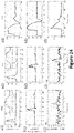
- figure 24 researchers have studied the electrical and optical responses of ⁇ OLEDs small molecules under pulsed excitation : the figure 24 show the excitation signal, the electrical response and the optical response for pulses of 800ps, 1ns and 20 ns.
- FIGS 25A & 25B researchers have studied the electrical and optical responses of ⁇ OLEDs polymers under pulsed excitation : the figures show the excitation signal, the electrical response and the optical response for pulses of 300ps up to 1ns. ⁇ Polymer-based ⁇ OLEDs respond at 300ps, a first in the world.
Landscapes
- Engineering & Computer Science (AREA)
- Physics & Mathematics (AREA)
- Electromagnetism (AREA)
- Computer Networks & Wireless Communication (AREA)
- Signal Processing (AREA)
- Optics & Photonics (AREA)
- Microelectronics & Electronic Packaging (AREA)
- Manufacturing & Machinery (AREA)
- Electroluminescent Light Sources (AREA)
Abstract
Description
- The present invention relates to the principle of design and production of matrix light emitters based on organic optoelectronics, such as organic light-emitting diodes (OLEDs), making it possible to emit variable light intensities for high-speed optical communication. These emitters require only limited technological complexity, making them suitable for use in signage and packaging on embedded objects, possibly on flexible substrates.
- Over the last few decades, light-emitting diodes (LEDs) have been widely studied in the field of Optical Wireless Communications (OWC) due to their predominance in high-end TVs and other display technologies. The field of short-range OWCs brings new applications requiring ultra-high data rates, such as Optical Network-on-Chip (OnoC), optical interconnects for artificial intelligence (A.I.), optical hardware accelerators and rotary joints for space systems, industry and the Internet.
- For these applications, increasingly higher data rates are desirable and requirements above 10 GB/s are beginning to appear. However, commercially available LEDs have limitations partly due to the high electrical response time of these components and more specifically their parasitic capacitance, so LEDs cannot achieve these objectives.
- The article "Towards 10 Gb/s orthogonal frequency division multiplexing-based visible light communication using a GaN violet micro-LED" by Mohamed S. Islim et al, demonstrates the interest of Gallium Nitride based micro-LEDs (GaN-LEDs) which offer smaller parasitic capacities and therefore higher bandwidths. The article also discusses µ GaN-LEDs offering bandwidths up to 300 MHz and data rates up to 7.9 Gb/s.
- Researchers and applicants have deposited two patents :
EP17306292.8 EP17306293.6 - One aim of the invention is to combine in a matrix form several fast OLEDs of different sizes to significantly increase the transmission rate to the level of what is practised in traditional telecommunications (∼10Gbit/s and above).
In order to integrate several micro-LEDs on the same substrate, it was necessary to adapt the cathode and anode stack to have light-emitting areas with different surfaces while maintaining a very fast response and analysis time. - Here, the invention presents a light emitting system intended for optical communication, having several OLEDs whose activation allows to obtain different levels of light intensity corresponding to different levels of light modulation, and which comprises :
- an organic optoelectronic device with OLEDs, the organic optoelectronic device having laterally separated actuatable zones on a substrate which supports :
- a first layer formed by several transparent and conductive anodes laterally separated by engravings, each anode Ai having a specific geometric pattern MAi ;
- a second layer for insulation on parts of the first layer, serving to electrically insulate the anodes so as to have separated anodes and the second layer for insulation having a thickness e1 ;
- a third layer having a thickness e2 and comprising at least one stack of organic layers ;
- a fourth layer in metal having a thickness e3, and composed of several cathodes laterally separated from each other and covering said stack of organic layers, each cathode Kj having a specific geometrical pattern MKj ;
- lateral separation profiles of the cathodes and of organic layers, to electrically insulate the cathodes, so as to have separated cathodes, the lateral separation profiles having a thickness e4 greater than e1+e2+e3, and being deposited on the first layer or on the second layer,
- the covering of the anodes, the stack of organic layer, and the cathodes, being realized so as to face each other:
- separated anodes and a common cathode ;

- separated anodes and separated cathodes ; and/or

- a common anode and separated cathodes ;

-
- a power supply, electrical wires and electrical contacts connected to the anodes and cathodes for their voltage supply so as to allow during an activation :
- a switching on of a combination of actuatable zones, the surface of which is less than or equal to the common surface of the facing activated anodes and activated cathodes ;
- connected to the electric wires, means for selective activation and displaying, to activate and display at each activation a total luminous surface which varies according to the number of actuatable zones turned on, so as to obtain different levels of luminous intensity of the system corresponding to different levels of light modulation, for different activations.
- Preferably, the cathodes Kj have specific geometrical patterns MKj different from the geometrical patterns MAi specific to the anodes.
- Preferably, the cathodes Kj have specific geometrical patterns MKj different from each other, and/or the geometrical patterns MAi specific to the anodes have specific geometrical patterns MKj different from each other.
- Advantageously, the OLEDs are easy to integrate on silicon substrate or on III-V substrates for use in onboard optics or for organic photonic above IC.
- The system can present means for selective activation and displaying, which are configured to enable at least 3 levels of light intensity to be achieved with the actuatable zones :
- a first level of light intensity, by the activation of one actuatable zone, by the combination of an activated anode, and an activated cathode facing the anode,
- a second level of light intensity by the activation of two actuatable zones :
- by a combination of at least two activated anodes facing at least one activated cathode, or
- by a combination of at least one activated anode facing at least two activated cathodes,
- a third level of light intensity by the activation of three actuatable zones :
- by a combination of at least three activated anodes facing at least one activated cathode, or
- by a combination of at least one activated anode facing least three activated cathodes, or
- by a combination of at least two activated anodes facing least two activated cathodes.
- The OLEDs forming the organic Opto-Electronic device and emit a light impulse can have a time response below 10ns, in response to an electrical impulse having a pulse duration time below 10ns.
- The challenge solved by the inventors is to make a component consisting of several fast OLED emitters.
- Two obstacles are overcome, the first obstacle is based on classical display techniques that use the decomposition of the display screen into pixels arranged at the intersections of rows and columns of a grid (or matrix) of horizontal and vertical interconnections. Note that in a display, the pixels all have the same size, therefore at similar current density they have the same luminous intensity, this does not allow to realize light sources of different light intensities corresponding to the different levels of modulation to be able to achieve a higher throughput.
- The second obstacle concerns the response time of these light emitters. The interconnection circuits of the pixel-based displays introduce serial resistors and parasitic capacitances that limit the bandwidth to several 100 Hz.
- In order to design ultra-fast OLED light arrays, researchers and applicants seek to combine microwave technologies (ultra-fast response) and OLED display technology (electrode stacking) by structuring them in the form of arrays. It is possible to structure patterns in OLEDs in different ways, either at the anode, at the cathode, or by a combination of both. (common anode - separate cathodes; separate anodes - common cathode; combination)
- Other advantages and characteristics of the disclosed devices and methods will become apparent from reading the description, illustrated by the following figures, where:
-
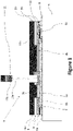
Figure 1 represents the organic optoelectronic device of the OLEDs type. -
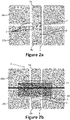
Figure 2a represents a top view of the organic optoelectronic device according to the invention with Co-Planar Waveguide electrodes (CPW)in Ground-Signal-Ground (GSG) configuration, without: the lateral separation profiles, the organic layer and the fourth layer of metal. -
Figure 2b represents a top view of the organic optoelectronic device according to the invention of CPW electrodes in GSG configuration {2x2 OLED matrix; 2 cathodes (one first cathode K1+K'1 with metal on the first side of the lateral separation profile; one second cathode: K2+K'2 with metal on the second side of the lateral separation profile) x 2 anodes OLED matrix}. -
Figure 3a represents a perspective view of the organic optoelectronic device offigure 2a and 2b , according to the invention of CPW electrodes in GSG configuration with two separated anodes, without : the lateral separation profiles, the organic layer and the fourth layer of metal. -
Figure 3b represents a perspective view of the organic optoelectronic device offigure 2a and 2b , according to the invention in CPW HP (GSG) configuration {2x2 OLED matrix; 2 cathodes (one first cathode K1+K'1 with metal on the first side of the lateral separation profile; one second cathode: K2+K'2 with metal on the second side of the lateral separation profile) x 2 anodes OLED matrix}. -
Figure 4a represents a top view of the organic optoelectronic device according to the invention in biplanar (microstrip) configuration, without: the lateral separation profiles, the organic layer and the fourth layer of metal, the numbers refer to the anode (A1, respectively A2+A'2, respectively A3+A'3) responsible for the activation of the zone (1, respectively 2, respectively 3),. -
Figure 4b represents a top view of the organic optoelectronic device according to the invention in biplanar (microstrip) configuration (3x3 OLED matrix; 3 cathodes (K1, K2, K3) x 3 anodes OLED matrix), the numbers refer to the anode (A1, respectively A2+A'2, respectively A3+A'3) responsible for the activation of the zone (1, respectively 2, respectively 3). -
Figure 5a represents a perspective view of the organic optoelectronic device offigure 4a and 4b , according to the invention in biplanar (microstrip) configuration with three separated anodes, without the lateral separation profiles, the organic layer and the fourth layer of metal. -
Figure 5b represents a perspective view of the organic optoelectronic device offigure 4a and 4b , according to the invention in biplanar (microstrip) configuration (3x3 OLED matrix; 3 cathodes x 3 anodes OLED matrix). -
Figure 6 represents a 1 x 3 OLED matrix (1 cathode x 3 anodes OLED matrix), and elements with the following configuration: Separated anodes - Common cathode. -
Figure 6a represents a 1 x 3 OLED matrix (1 cathode x 3 anodes OLED matrix) with 3 actuatable zones. -
Figure 6b represents a separation of the anode into three zones (A1, A2, A3). -
Figure 6c represents a common cathode (K1). -
Figure 6d represents a complete structure of OLED matrix by superposition of the cathode with the anodes. -
Figure 7 represents a 1 x 3 OLED matrix (1 cathode x 3 anodes OLED matrix) with 3 actuatable zones with different levels of light intensity for the biplanar configuration; a) no light emission; b) low intensity light emission; c) medium intensity light emission; d) high intensity light emission. -
Figure 8 represents a 3 x 1 OLED matrix (3 cathodes x 1 anode OLED matrix) and elements with the following configuration: Common anode - Separated cathodes -
Figure 8a represents a 3 x 1 OLED matrix (3 cathodes x 1 anode OLED matrix) with 3 actuatable zones. -
Figure 8b represents a common anode (A). -
Figure 8c represents a separation of the cathode into three zones (K1, K2, K3). -
Figure 8d represents a complete structure of OLED matrix by superimposing the cathodes with the anode. -
Figure 9 represents a 3 x 3 OLED matrix (3 cathodes x 3 anodes OLED matrix) and elements with the following configuration: Separated anodes - Separated cathodes. -
Figure 9a represents a possible separation of the anode into three zones, with points of strangulation. -
Figure 9b represents a 3 x 3 OLED matrix (3 cathodes x 3 anodes OLED matrix) with 6 actuatable zones. -
Figure 9c represents a separation of the anode into three zones (A1, A2, A3). -
Figure 9d represents a separation of the cathode into three zones (K1, K2, K3). -
Figure 9e represents a complete structure of OLED matrix by superimposing the cathodes with the anodes. -
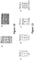
Figure 10 represents a 2 x 2 OLED matrix (2 cathodes x 2 anodes OLED matrix), and elements with the following configuration: Separated anodes - Separated cathodes. -
Figure 10a represents a separation of the anode into two zones (A1, A2). -
Figure 10b represents a separation of the cathode into two zones (K1, K2). -
Figure 11 represents a 2 x 2 OLED matrix (2 cathodes x 2 anodes OLED matrix) with 3 actuatable zones with different levels of light intensity for the CPW configuration; a) no light emission; b) low intensity light emission; c) medium intensity light emission; d) high intensity light emission. -
Figure 12 represents the electrical schematic equivalent to the 2x2 OLED matrix (2 cathodes x 2 anodes OLED matrix) of the CPW configuration. -
Figure 13 represents the total voltage as a function of time, varying on 4 different voltage levels, each level is associated to a combination of two bits. -
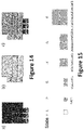
Figure 14 represents a represents a 3 x 3 OLED matrix (3 cathodes x 3 anodes OLED matrix) and elements with the following configuration: Separated anodes - Separated cathodes ; a) a separation of the anode into three zones (A1, A2, A3) ; b) a separation of the cathode into three zones (K1, K2, K3) ; c) a complete structure of OLED matrix by superimposing the cathodes with the anodes. -
Figure 15 represents 6 possible states of different light intensity levels. -
Figure 16 represents the electrical schematic equivalent to the 3x3 OLED matrix (3 cathodes x 3 anodes OLED matrix) of the biplanar configuration. -
Figure 17 represents the light emitting system with the organic optoelectronic device with OLEDs (3 cathodes x 3 anodes OLED matrix), the power supply and the means for selective activation and displaying. -
Figure 18 represents a represents a 4 x 4 OLED matrix (4 cathodes x 4 anodes OLED matrix), and elements with the following configuration: Separated anodes - Separated cathodes ; a) a separation of the anode into four zones (A1, A2, A3, A4) ; b) a separation of the cathode into four zones (K1, K2, K3, K4) ; c) a complete structure of OLED matrix by superimposing the cathodes with the anodes. -
Figure 19 represents 8 possible states of different light intensity levels. -
Figure 20 represents an anode structuring process by engraving. -
Figure 21 represents an anode structuring process by metallization. -
Figure 22 represents a process for the realization of undercut resin inducing cathode separation. -
Figure 23 represents a deposition of organic and metallic layers. -
Figure 24 represents the study of the electrical and optical responses of µOLEDS small molecules under pulsed excitation :the figures show the excitation signal (a1, a2, a3), the electrical response (b1, b2, b3) and the optical response (c1, c2, c3) for pulses of 800ps (a1, b1, c1), 1ns (a2, b2, c2) and 20 ns (a3, b3, c3). -
Figures 25A &25B represents the study of the electrical and optical responses of µOLEDS polymers under pulsed excitation : the figures show the excitation signal (a1, a2, a3, a4, a5), the electrical response (b1, b2, b3, b4, b5) and the optical response (c1, c2, c3, c4, c5) for 300ps pulses (a1, b1, c1), 0.4ns (a2, b2, c2), 600ps (a3, b3, c3), 800ps (a4, b4, c4) and 1ns (a5, b5, c5). - The invention relates to a
light emitting system 1 intended for optical communication, which presentsseveral OLEDs 2 whose activation allows to obtain different levels of light intensity corresponding to different levels of light modulation. - The
light emitting system 1 is represented schematically onfigure 17 . - The
light emitting system 1 comprises : - an organic
optoelectronic device 3 withOLEDs 2, as represented onfigure 1 , the organicoptoelectronic device 3 having laterally separatedactuatable zones substrate 5 which supports :- a
first layer 6 formed by several transparent andconductive anodes engravings 7, each anode Ai having a specific geometric pattern MAi ; - a second layer for
insulation 8 on parts of thefirst layer 6, serving to electrically insulate theanodes - a
third layer 9 with a thickness e2 comprising at least one stack oforganic layers organic layers anodes organic layers second layer 8 are inert) ; - a
fourth layer 10 in metal having a thickness e3, and composed ofseveral cathodes organic layers - lateral separation profiles 11 of the
cathodes organic layers cathodes first layer 6 or on thesecond layer 8, - the covering of the
anodes organic layer cathodes - separated anodes and a common cathode ;

- separated anodes and separated cathodes ; and/or

- a common anode and separated cathodes ;

-
zones zone - a
- As represented on
figure 17 , thelight emitting system 1 presents also: - a
power supply 13, electrical wires and electrical contacts connected to the anodes and cathodes for their voltage supply so as to allow during activation :- the switching on of a combination of
actuatable zones
- the switching on of a combination of
- connected to the electric wires, means for selective activation and displaying 14, to activate and display at each activation a total luminous surface which varies according to the number of the
actuatable zones system 1 corresponding to different levels of light modulation, for different activations. - The
power supply 13 can be a cell, a battery or a photovoltaic cell. - Advantageously, as represented on
figures 1 and22 , the lateral separation profiles 11 are produced by photolithography and development and have a stack of two resins deposited on each other with anon-photosensitive resin 11a deposited in contact with thefirst layer 6 or thesecond layer 8, and a positivephotosensitive resin 11b on thenon-photosensitive resin 11a. - In a possible embodiment, the lateral separation profiles 11 are produced by photolithography and development, and the
second layer 8 is a negativephotosensitive resin 11a. - Advantageously, the lateral separation profiles 11 have a thickness at least four times greater than the sum of the thicknesses e1+e2+e3. More precisely, the thickness of the lateral separation profiles 11 is one to several micrometers.
- Advantageously, the lateral separation profiles 11 have inverted profiles whose tip is in contact with the
first layer 6 or thesecond layer 8 and whose base widened with respect to the tip is located above thefourth layer 10. - Advantageously, the lateral separation profiles 11 have a
long part 11a (composed of negative photosensitive) in contact with the layer forinsulation 8 and ahead 11b on thelong part 11b, thehead 11b is larger than thelong part 11a, so as to create a space between thelong part 11a and thecathodes - The
OLEDs 2 can be milli-OLEDs and/or micro-OLEDs. - More preferably, the
OLEDs 2 are micro-OLEDs.
They can form the organicoptoelectronic device 3 emitting a light impulse which can have a time response below tens of ns, for instance10ns, in response to an electrical impulse having a pulse duration time below 10ns. - The organic
optoelectronic device 3 can have two different possible structure. - As shown in
figures 2a, 2b ,3a and 3b , the organicoptoelectronic device 3 presents a CPW electrodes in GSG configuration (GSG shape: ground - signal - ground). - The organic
optoelectronic device 3 presents anode and cathode parts outside theactuatable zones 4, as represented onfigure 7 . The actuatable zones are situated where the OLEDs 2 (anode layer 6,organic layer 9, cathode layer 10) are.
These so-called outer parts allow the anode and the cathode to be connected to the means for selective activation and displaying 14, represented onfigure 17 . - Advantageously in this configuration, the external parts of the cathodes are doubled to insure a 50 ohm characteristic impedance so as to maximize increase the speed of the response, for instance for one
cathode 10a (respectivelycathode 10b), there are two external parts K1 and K'1 (respectively K2 and K2'). - When the layers are deposited in this configuration, the lateral separation profiles 11 form a separation line allowing the
fourth metal layer 10 to be separated in two and each part to be connected to the corresponding outer cathode parts. - In this configuration, the
cathodes anodes engravings 7. - Advantageously, the width of the cathode planes (K1 with K1' or K2 with K2') is at least three times as large as the anode (A1 or A2). The widths of the
engraving 7 separating the anode A1 from A2 are few micrometers to few hundred of micrometers. - As shown in
figures 4a, 4b ,5a and 5b , the organicoptoelectronic device 3 presents a biplanar shape (microstrip). - Advantageously, the anodes (A2, A3) have a "twin" anode (A2', A3') allowing a lower serial resistance, a better pulse delivery and therefore a faster response of the actuatable zones.
- In this configuration, a
ground plane 15 is located below thesubstrate 5 on which is the organicoptoelectronic device 3. - Advantageously, the organic
optoelectronic device 3 have different shape, more preferably a star shape (or a sun shape) and each branch is an electrode. - Advantageously, the number of branches can be designed adequately, a greater number of branches allows to delimit a greater number of actuatable zones.
- The
engravings 7 allow to separate thedifferent anodes - Advantageously, the cathodes occupy a part of the branches of the star and the anodes the other part, for example, the cathodes are located on the left branches and the anodes on the right branches, more precisely, the anodes follow each other then the cathodes follow each other, there is no alternation between cathode and anode.
- In one possible embodiment, the anodes and cathodes follow each other intermittently (Anode -cathode - anode - cathode - ...).
- As represented on
figure 6 , advantageously, the organicoptoelectronic device 3 is a matrix which is rectangular or square, and which presentsOLED 2 with different forms configured to realize the matrix. More precisely, thecathodes anodes - As represented on
figure 1 , the organicoptoelectronic device 3 of theOLEDs 2 can have a metallic contour and/or metallic lines and/ormetallic areas 12 to increase the conductivity of theanodes first layer 6 and allowing to keep an actuatablezone
Depending on the dimensions of the zones you would like to have lit (actuatable zones - The
actuatable zones zone OLED 2. - The
anodes cathodes - For example, the
anodes OLEDs 2. - The second layer for
insulation 8 can have dyes and/or quantum dots to absorb the light emitted from the separatedactuatable zones
Advantageously, the second layer forinsulation 8 is on parts of thefirst layer 6 or parts of the stack oforganic layers anodes - Advantageously, the
third layer 9 comprises: polymers, small molecules, phosphorescent materials, heat actuatable materials. - As represented on the
figures 6-11 ,14-15 ,18-19 , the cathodes Kj can have specific geometrical patterns MKj different from the specific geometrical patterns MAj specific to the anodes. - In another embodiment, the cathodes Kj have specific geometrical patterns MKj different from each other and/or the geometrical patterns MAj specific to the anodes having specific geometrical patterns MKj different from each other.
- Preferably, the patterns are geometrical because the patterns are chosen to have precise
actuatable zones - Preferably, the geometrical patterns MAi and MKj are circles or polygons, more preferably, the polygons have a mathematical ratio allowing the repetition of the pattern. For example, in the case of parallel lines of the same size, the mathematical ratio is a proportionality coefficient equal to 1; in the case of an L shape composed of 3 micro-OLEDs, the mathematical ratio follows this sequence: (n+1)= (n) + 2, n representing the number of micro-OLEDs in the pattern, the following sequence means that the next pattern (n+1), adds 2 micro-OLEDs to the number of micro-OLEDs of the previous pattern (n).
- The activation of cathodes and anodes can be sequential or parallel.
- Advantageously, the electrical wires are connected to the
first layer 6 and to thefourth layer 10; and wherein thefirst layer 6, thefourth layer 10 and aground plane 15 are separated by gaps without conductive material, the gaps having a size so as to adapt the speed of propagation of the electrical pulse in thesystem 1 for limiting the reflections due to the passage of the electrical impulse between electrical wire and the electrodes (anodes and cathodes). - The gaps can have a size so that an effective dielectric permittivity of the organic
optoelectronic device 3 equal to the dielectric permittivity of the electrical wires delivering the electrical impulse. - Advantageously, the
first layer 6, thefourth layer 10 and theground plane 15 are structured to integrate an excitation or a characterization circuit, including at least a resistance, a capacitance and/or an inductance, which are disposed in series and/ or parallel. - Advantageously, as represented on
figures 5a and 5b , thesubstrate 5 comprises : - the
ground plane 15 is on one side of thesubstrate 5, and - the
first layer 6 and thefourth layer 10 are tracks on the other side of thesubstrate 5 and are electrically linked to theground plane 15 with vias. - The
first layer 6 can extend between twoground planes 15 on the same side of thesubstrate 5, at equal distance of the twoground planes 15, and is separated from the twoground planes 15 with some gaps G without conductive material.
The transversal dimension T of thefirst layer 6 and the transversal dimension of the gap G between saidfirst layer 6 and each of the twoground planes 15 can be such that the effective dielectric permittivity εr effective defined by εreffective = 1 +
ε r 0 the dielectric permittivity of the electrical wire. - Thus,
εr is the dielectric permittivity of thedielectric substrate 5, γ1, γ2 and γ3 are geometrical parameters,


interval 

interval 
dielectric substrate 5, and εr represents the relative dielectric permittivity of thedielectric substrate 5. T represents the transversal dimension of theanode anode cathode - These ground planes 15 are present on either side of the
anode
For a given dielectric, the characteristic impedance of planar electrodes to produce fast opto-electronic components is given mainly by the form factor defined by the ratio γ1. - For example, the condition for obtaining the same effective relative dielectric permittivity for the electrodes as for the cables, results in ε r effective = εr = 1,5.
- So, we obtained a relation between T, G and the ratio T / (T + 2G). To reduce or cancel these reflections, it is therefore possible to modify the geometry of the µ-OLED and in particular the ratio T / (T + 2G).
- Considering a glass substrate (εr = 7.75) of thickness H = 1000 µm, and tin oxides and indium (ITO) electrodes with a conductivity σ = 5.95e5 of 100 nm thickness.
- Given a predefined Transversal dimension T value, we calculate Gap G value such as εr effective = 1.5 to obtain the following table of dimensions:
T G T/(T+2G) 100µm 30µm 0.625 200µm 60µm 0,625 500µm 146µm 0,631 1mm 267µm 0,651 2mm 433µm 0,697 3mm 548µm 0,732 4mm 640µm 0,757 5mm 720µm 0,776 10mm 1027µm 0,829 - In reference to
figures 2a, 2b ,3a, 3b , different coplanar electrode structures are illustrated. - The
dielectric substrate 5, can be a glass sample covered with aconductive layer 6, for example with ITO (figure 2a ). Electrodes are structured by removing the conductive layer by at least two parallel continuous lines of transversal dimension G. This allows creating central electrodes of transversal dimension T separated by a distance G from twoground planes 15, (cathodes in thefigure 2a ). This dimensioning makes it possible to ensure continuity of propagation with the excitation source and its connection (the same principle applies to other target frequencies above 1 GHz, for example). Indeed, the gaps G is dimensioned to adapt the speed of propagation of the electrical pulse in the device for limiting the reflections due to the passage of the electrical impulse between electrical wire and the planar electrode. Moreover, the gaps G have a size so that an effective dielectric permittivity of the Organic Opto-Electronic device 3 equal to the dielectric permittivity of the electrical wire delivering the electrical impulse (plus or minus 10%). - The following table illustrates the different geometries allowing the reduction of the impulsions:
Co-planar electrodes Bi-planar electrodes Substrate h T G Z h t T Z Glass εr=7,75 1100µm 1000µm 550µm 50.0Ω 1100 µm 100nm(Au) 1325 µm 50.0Ω 1100µm 500µm 175µm 50.2Ω 1100µm 100µm 31µm 50.2Ω 900µm 100µm 31µm 50.2Ω Silicon εr= 11,9 275µm 250 µm 125µm 49.9Ω 275 µm 100nm(Au) 219 µm 50.0Ω 275µm 50 µm 195µm 50.0Ω 525µm 500µm 247 µm 50.0Ω 525 µm 100nm(Au) 418 µm 50.0Ω 72 5 µm 500µm 267 µm 50.0Ω 725 µm 100nm(Au) 577 µm 50.0Ω 72 5 µm 1000µm 437 µm 50.0Ω Germanium εr=16 500µm 1000µm 525µm 50.0Ω 500 µm 100nm(Au) 286 µm 50.0Ω GaN εr= 5,35 500µm 1000µm 130µm 50.0Ω 500 µm 100nm(Au) 822 µm Soft substrate (PET) εr=5 500µm 1000µm 118µm 50.0Ω 500µm 500µm 69µm 50.0Ω plexiglass εr= 3,5 500µm 242µm 20µm 50.0Ω - In a possible embodiment, the
system 1 comprises : - the
first layer 6 or thefourth layer 10 can be theground plane 15 ; and/or - the
ground plane 15 is on one side of thesubstrate 5, and thefirst layer 6 and thefourth layer 10 are tracks on the other side of thesubstrate 5 and are electrically linked to theground plane 15 with vias ; and/or - the geometry of the
first layer 6 and of theground plane 15 in regard to the geometry of thefourth layer 10 create an impedance of the device equal to 50 ohms or 75 ohms ; and/or - the
first layer 6 and/or thefourth layer 10 presents a conductive and transparent layer; and/or - the
fourth layer 10 is the cathode made of ITO (indium tin oxide), and thefirst layer 6 is the anode and is made with a metallic layer; and/or - the
dielectric substrate 5 is Glass, silicon, silicon oxide, silicon oxide on silicon, polymers or flexible substrate ; and/or - the Organic Opto-
Electronic device 3 is composed of OLEDs or Organic photodiodes; and/or - the
system 1 comprises superposed on thedielectric substrate 5, thefirst layer 6 with a first extremity; thefourth layer 10, with another extremity covering partially said first extremity and saidorganic layer stack actuatable zone Electronic device 3; and/or - the Micro Organic Opto-
Electronic device 3 being modeled with a resistance in series with a diode which is in series with a resistance, or by a resistance in series with a dynamic resistance, at least one junction capacitance in parallel with the diode and the resistance, or in parallel with the dynamic resistance, for modelling theactuatable zone - the
first layer 6 and/or thefourth layer 10 presents a transparent and conductive layer; and/or - the branch connecting the two arms comprises one or several photonic elements; and/or
- the photonic element is chosen among the list: a waveguide, a grating, a Distributed Feedback mirror, a laser cavity, a laser cavity made of distributed feedback mirrors, a photonic crystal, a laser cavity made of a defect in a photonic crystal.
- There are three different types of activation combinations:
- In this case, the µOLEDs are defined by cutting the anode into several zones electrically separated from each other. This separation is achieved, for example, by etching the transparent and conductive ITO layer.
- In the example of
Figure 6 , the anode is structured in three contacts A1, A2 and A3 obtained by etching, through which it is possible to switch on the µOLED ofgroup 1, the 3 µOLEDs ofgroup 2, or the 5 µOLEDs ofgroup 3. To activate theµOLED 1, a voltage must be applied between the contacts A1 and the common cathode K, and for theµOLEDs 2 it will be between the anodes A2 and the common cathode K and finally for theµOLEDs 3 between A3 and K. - In
figure 7 , image a) representslevel 0, i.e. a light emission of zero intensity (0 µOLED on). Image b) representslevel 1, i.e. a low intensity light emission (1/9 µOLED on or 1 µOLED out of 9). Image c) representslevel 2, which is a medium intensity light emission (4/9 µOLED on or 4 µOLED out of 9). And image d) represents level 3 a high intensity light emission - 9/9 µOLED on or 9 µOLED on 9). - In the classical display, the pixels have only two states: on or off, from a light point of view it is a 0 or a 1. In terms of information transmission, with pixels there are only two states, while with matrix OLEDs the number of states depends on the number of cathodes and anodes, for example with 3 anodes and 1 cathode, as shown in
figure 6 , there are at least 4 possible states, as shown infigure 7 . - In this configuration, the final patterns are not implemented by different areas at the transparent and conductive anode, but by different cathodes K1, K2, K3, as shown in
Figure 8 . The difficulty in separation the cathodes is important because of the manufacturing process of the OLEDs themselves. In this case, the claims of inverted profiles apply. -
Approach 2. (common anode, separate cathodes) may show limitations in some particular cases, especially when some patterns are almost nested in others, and when the electrical contacts to the excitation source are difficult to make. -
Figure 9.a illustrates an example of difficult nesting, creating two strangulation points. These choke points are likely to induce a high contact resistance in case of engraving, thus making the grip with A1 difficult or inefficient. This can result in differences in brightness of the areas A1 compared to A2 or A3. In such a case, an alternative consists in redistributing the patterns by returning others to the cathode, as shown infigure 9 . For example, one can transfer the µOLEDs fromlevel 2, by taking the contacts K1 and K2. Resin lines structured in undercut resin would then allow to partition the cathode. - Advantageously, each actuatable zone can be turned on separately.
- In
figure 11 , image a) representslevel 0, i.e. a light emission of zero intensity (0 µOLED on). Image b) representslevel 1, i.e. a low intensity light emission (1/9 µOLED on or 1 µOLED out of 9), this level is obtained by activating the actuatable zone (1 µOLED) of the center by activating the anode A1 and the cathode K2. Image c) representslevel 2, which is a medium intensity light emission (4/9 µOLED on or 4 µOLEDs out of 9), this level is obtained by activating the actuatable zones (4 µOLEDs) of the center and the bottom by activating the anode A1 and the cathodes K1 & K2. And image d) represents level 3 a high intensity light emission (9/9 µOLED on or 9 µOLEDs on 9), this level is obtained by activating all the actuatable zones (9 µOLEDs) (center, bottom and top) by activating the anodes A1 & A2 and the cathodes K1 & K2. - It is then possible to switch on
level 1 by making contact between anode A1 and cathode K1;level 2 will be the combination of anode A1 and cathode K1 and K2; and to switch onlevel 3, all contacts A1, A2 and A3; K1, K2 and K3 must be made. - Another alternative to the problem of strangulation or nested patterns would be to print very fine conductive tracks of noble metal such as gold, for example, on the anode patterns. This improves the injection of current and its flow both within the patterns and at the choke points.
- The
system 1 for transmitting withseveral OLEDs 2 can be a matrix of organic light emitters, e.g. a 3 x 3 device (anodes x cathodes), as shown infigure 9.e . TheOLEDs 2 are structured and combined to obtain four different light intensities corresponding to the four modulation levels. - In this example, the structuring of this matrix is based on inverted profiles. The activation of the different parts of the matrix can be done by the activation of a combination of anode and cathode, in fact to switch on the different levels, a judicious combination of cathode / anode is activated.
In an example of embodiment, as shown infigure 18 , it is possible to emit by combining the anode(s) and cathode(s) up to a minimum of 8 states of different levels, shown infigure 19 . - In the configuration shown, the switching speed is limited by the series resistance and the parasitic capacitance of the largest OLED (64 µOLED). The series resistance decreases with the width of the electrodes and the parasitic capacitance increases with the surface of the OLED. So the capacitance increases faster than the resistance.
- For example, as shown in
figure 13 , by using 4 levels, it is possible to assign 2 bits to each level as opposed to a 2-level transmission. The transmission will therefore be doubled for the same time and speed compared to a 2-bit signal. In this example : -
level 0 corresponds to bit 00 (all OLEDs are off), -
level 1 corresponds to bit 01 (OLED 1 is on), -
level 2 corresponds to bit 11 (OLEDs ofgroup -
level 3 corresponds to bit 10 (all OLEDs are on). - In this example, it is possible to assign 3 bits (and starting 4th bit) and to have more than 4 levels:
Level bit OLEDs 0 000 off 1 001 OLED 1 on2 010 OLED 2 on3 011 OLEDs 1 & 2 on4 100 OLED 3 on5 101 OLEDs 1 & 3 on6 111 OLEDs 2 & 3 on7 1000 OLEDs 1 & 2 & 3 on - The means for selective activation and displaying 14 can be a processor, a computer or a microcontroller.
- Preferably, the means for selective activation and displaying 14, activate one couple (one pair) anode-cathode to turn on one actuatable zone.
- Advantageously, the means for selective activation and displaying 14 of the separated
actuatable zones - The means for selective activation and displaying 14 can be configured to enable at least 3 levels of light intensity to be achieved with the
actuatable zones -
- a first level of light intensity, by the activation of one
actuatable zone - a second level of light intensity by the activation of two
actuatable zones - by a combination of at least two activated anodes facing at least one activated cathode, or
- by a combination of at least one anode facing at least two cathodes,
- a third level of light intensity by the activation of three
actuatable zones - by a combination of at least three anodes facing at least one cathode, or
- by a combination of at least one anode facing least three cathodes, or
- by a combination of at least two anodes facing least two cathodes.
-
- a first level of light intensity, by the activation of one
actuatable zone - a first activated anode, and
- a first common cathode activated facing the first anode,
- a second level of light intensity, by the activation of at least two separated
actuatable zones - a first activated anode, and a second activated anode, and
- a first common cathode activated facing the two anodes,
- a third level of light intensity, by the activation of at least three separated
actuatable zones - a first activated anode, a second activated anode and a third activated anode, and
- a first common cathode activated facing the three anodes.
-
- a first level of light intensity, by the activation of one
actuatable zone - a first common anode activated, and
- a first activated cathode facing the first anode,
- a second level of light intensity, by the activation of at least two separated
actuatable zones - a first common anode activated, and
- a first activated cathode and a second activated cathode facing the first common anode,
- a third level of light intensity, by the activation of at least three separated
actuatable zones - a first common anode activated, and
- a first activated cathode, a second activated cathode and a third activated cathode facing the first common anode.
-
- a first level of light intensity, by the activation of one
actuatable zone - a first activated anode, and
- a first cathode activated facing the first anode,
- a second level of light intensity, by the activation of at least two separated
actuatable zones - a first activated anode and a second activated anode,
- a first activated cathode facing the first anode and a second activated cathode facing the second anode,
- a third level of light intensity, by the activation of at least three separated
actuatable zones - a first activated anode, a second activated anode and a third activated anode ,
- a first activated cathode facing the first anode, a second activated cathode facing the second anode and a third activated cathode facing the third anode.
- The
substrate 5 can be transparent for a Top Emission and not transparent for a Bottom Emission. More precisely, thesubstrate 5 is a flexible substrate or made of glass, silicon, silicon oxide, silicon oxide on silicon, polymer, gallium nitride, diamond. - Advantageously, the
fourth layer 10 is a metallic layer and depending on the thickness, the metallic layer 10 (the fourth layer) can be transparent (20nm thick) or opaque (> 100nm). More precisely, in the case of a Top Emission, a transparent cathode will be used and for a Bottom Emission, an opaque cathode will be used. - As represented on
figures 20-23 , the invention relates to also a process of manufacturing an organicoptoelectronic device 3 of the OLED type comprising : - the manufacturing (realization) on a
substrate 5 of the anodes by :- depositing a first transparent and
conductive layer 6 on thesubstrate 5, formed by several transparent and conductive anodes separated laterally byengravings 7; - predefined structuring of a specific geometric pattern for each anode ;
- depositing a first transparent and
- the deposition of a second layer for
insulation 8 on parts of thefirst layer 6 and on theengravings 7, serving to electrically insulate theanodes - the realization of lateral separation profiles 11 of thickness e4 ;
- the deposition of the
third layer 9 oforganic layers anodes insulation 8, and the lateral separation profiles 11 ; - deposition of the fourth layer of
metal 10 with a thickness e3, by evaporation of a metal on theorganic layers cathodes
the thickness e4 being greater than e1+e2+e3,
the covering of theanodes organic layers cathodes - separated anodes and a common cathode ;
- separated anodes and separated cathodes ; and/or
- a common anode and separated cathodes ;
actuatable zones zone - The process can be use photolithography and engraving, and advantageously comprises the following steps:
- for structuring the
anodes - deposition of a photosensitive resin R1 on the
first layer 6 ; - positioning of a photolithography mask T1, whose openings allow the predefined structuring of a specific geometric pattern for each anode, on the photosensitive resin R1 ;
- photolithography by exposure of the photosensitive resin R1 through the first openings, development, engraving in the first layer to make the separated anodes and cleaning of the resin ;
- deposition of a photosensitive resin R1 on the
- for depositing the second layer for insulation 8 :
- deposition of a second layer for
insulation 8 comprising a photosensitive resin R2 with a thickness e1 on the separated anodes constituting thefirst layer 6 ; - positioning of a photolithography mask T2 ;
- exposure photolithography and development of the second layer for
insulation 8 ;
- deposition of a second layer for
- for the realization of lateral separation profiles 11 :
- deposition of at least one photosensitive resin R3 on the anodes and the second layer for
insulation 8 ; - positioning of a photolithography mask T3 whose openings make it possible to create the lateral separation profiles 11 ;
- UV exposure photolithography and development of the photoresist to produce the lateral separation profiles 11.
- deposition of at least one photosensitive resin R3 on the anodes and the second layer for
- Advantageously, before the second layer for
insulation 8 is applied to thefirst layer 6, the following steps are carried out : - deposition of a layer of photosensitive resin R2 on the
anodes - positioning of a photolithography mask T2 whose openings define the locations intended to receive a metallic layer to produce a metallic contour and/or metallic lines and/or
metallic area 12; - photolithography by exposing the positive photosensitive resin layer R2 through the openings and developing ;
- deposition of the
metal layer 12 in such a way that the areas of theanodes second layer 8 are covered by the metal layer in direct contact with the first layer; - cleaning the photosensitive resin layer R2 to remove it.
- Advantageously, before depositing the light-sensitive resin on the anodes and/or on the second layer for
insulation 8, a non-photosensitive resin is deposited on this light-sensitive resin, in order to produce inverted lateral separation profiles 11 which have : - a tip which is in contact with the layer formed by a plurality of separated anodes; and
- a base widened in relation to the tip and located above the layer formed by the separated cathodes.
- Advantageously, the photosensitive resin R1 deposited on the
first layer 6 is positive or negative, the photosensitive resin R2 forming thesecond layer 8 is negative, and the photosensitive resin R3 for making the lateral separation profiles 11 is positive. - The openings of the second mask T2 can be arranged on the second layer for
insulation 8, so that photolithography and etching of the second layer forinsulation 8 leave the spaces between the anodes filled by the second layer forinsulation 8. - The
first layer 6 can be an ITO layer to make theanodes cathodes - Advantageously, the gold-chromium is deposited just after the structuring (engraving) of the anode in order to improve the conductivity in the case of Bottom Emission. More precisely, in the case of Top Emission, the Gold-Chromium deposit is not necessary or even not useful and silver is used for the Top Emission and aluminum can be used in Bottom Emission.
- The organic
optoelectronic device 3 can be fabricated on different types of rigid substrates such as Glass, Silicon or Gallium Nitride with top emission. - In another possible embodiment, the manufacturing process can follow the following steps:
- Step 1 - the realization of the
anodes - ∘ Cleaning step
- ∘ Photolithography step
- ∘ Engraving step
- ∘ Cleaning step
- Step 2 - Metallization
- ∘ Cleaning step
- ∘ Photolithography step
- ∘ Metallization
- ∘ Lift-Off
- Step 3 - Structuring of the partition lines of the cathode in "cap profile"
- ∘ Cleaning step
- ∘ Photolithography on base plate of separation profile
- Step 4 - Organic layer and cathode deposition (Aluminum)
The last step in the OLED manufacturing process consists of depositing the organic and metallic layers.- ∘ Vacuum Thermal Evaporation
- ∘ Encapsulation
- In
figure 24 , researchers have studied the electrical and optical responses of µOLEDs small molecules under pulsed excitation :
thefigure 24 show the excitation signal, the electrical response and the optical response for pulses of 800ps, 1ns and 20 ns. - In
figures 25A &25B , researchers have studied the electrical and optical responses of µOLEDs polymers under pulsed excitation :
the figures show the excitation signal, the electrical response and the optical response for pulses of 300ps up to 1ns.
→ Polymer-based µOLEDs respond at 300ps, a first in the world. - The results of these matrix OLEDs reach world records, optical responses of less than 800ps have been recorded following an electrical excitation for ultra-short pulse durations on µOLEDs and 300ps for Polymer OLEDs. These worldwide results are a revolution for applications such as optical telecommunications, optical buses, Lifi, etc.
Claims (17)
- Light emitting system (1) intended for optical communication, having several OLEDs (2) whose activation allows to obtain different levels of light intensity corresponding to different levels of light modulation, and the system comprises:• an organic optoelectronic device (3) with OLEDs (2), the organic optoelectronic device (3) having laterally separated actuatable zones (4a, 4b) on a substrate (5) which supports:- a first layer (6) composed of several transparent and conductive anodes (6a, 6b, 6c), laterally separated by engravings (7), each anode Ai having a specific geometric pattern MAi;- a second layer for insulation (8) on parts of the first layer (6), serving to electrically insulate the anodes (6a, 6b, 6c) so as to have separated anodes, and the second layer for insulation having a thickness e1;- a third layer (9) having a thickness e2 and comprising at least one stack of organic layers (9a, 9b);- a fourth layer (10) in metal having a thickness e3, and composed of several cathodes (10a, 10b) laterally separated from each other and covering said stack of organic layers (9a, 9b), each cathode Kj having a specific geometrical pattern MKj;- lateral separation profiles (11) of the cathodes (10a, 10b) and of organic layers (9a, 9b), to electrically insulate the cathodes (10a, 10b) so as to have separated cathodes, the lateral separation profiles (11) having a thickness e4 greater than e1+e2+e3, and being deposited on the first layer (6) or on the second layer for insulation (8),- the covering of the anodes (6a, 6b, 6c), the stack of organic layers (9a, 9b), and the cathodes (10a, 10b), being realized so as to present facing each other:defining separated the actuatable zones (4a, 4b), each actuatable zone (4a, 4b) comprising at least one part of any cathode and at least one part of any anode facing each other,separated anodes and a common cathode;
 separated anodes and separated cathodes; and/or
 a common anode and separated cathodes;
 • a power supply (13), electrical wires and electrical contacts connected to the anodes and cathodes for their voltage supply so as to allow during an activation:a switching on of a combination of actuatable zones (4a, 4b),the surface of which is less than or equal to the common surface of the facing activated anodes and activated cathodes;• connected to the electric wires, means for selective activation and displaying (14), to activate and display at each activation a total luminous surface which varies according to the number of the actuatable zones (4a, 4b) turned on, so as to obtain different levels of luminous intensity of the system (1) corresponding to different levels of light modulation, for different activations.
 - The system (1) according to claim 1, wherein the cathodes Kj have specific geometrical patterns MKj different from the geometrical patterns MAj specific to the anodes.
- The system (1) according to claims 1-2, wherein the cathodes Kj have specific geometrical patterns MKj different from each other, and/or wherein the geometrical patterns MAi specific to the anodes have specific geometrical patterns MKj different from each other.
- The system (1) according to claims 1-3, wherein the organic optoelectronic device (3) is a matrix which is rectangular or square, and which presents OLED with different forms configured to create the matrix.
- The system (1) according to claims 1-4, wherein the cathodes (10a, 10b) and anodes (6a, 6b, 6c) being rectangular and/or L-shaped areas, and/or nested to form the matrix.
- The system (1) according to claims 1-5, wherein the OLEDs (2) are micro-OLEDs.
- The system (1) according to claims 1-6, wherein the first layer (6), the fourth layer (10) and a ground plane (15) are separated by gaps without conductive material, the gaps having a size so as to adapt the speed of propagation of the electrical pulse in the device for limiting the reflections due to the passage of the electrical impulse between electrical wire and the electrodes.
- The system (1) according to claim 7, wherein the gaps having a size so that an effective dielectric permittivity of the organic optoelectronic device (3) equal to the dielectric permittivity of the electrical wires delivering the electrical impulse.
- The system (1) according to claims 1-8, wherein:the anode (6a, 6b) extends between two cathodes (10a, 10b) on the same side of the substrate, at equal distance of the two cathodes (10a, 10b), and is separated from the two cathodes (10a, 10b) with some gaps (G) without conductive material;the transversal dimension T of the anode (6a, 6b) and the transversal dimension G of the gap (G) between said anode (6a, 6b) and each of the two cathodes (10a, 10b) are such that the effective dielectric permittivity εr effective defined by: 1+(εr- 1)/2*β(γ2)β(γ1) is equal to εr0 the dielectric permittivity of the electrical wire;where:
ε r is the dielectric permittivity of the dielectric substrate, γ1, γ2 and γ3 are geometrical parameters,


- The system (1) according to claims 1-9, wherein the ground plane (15) is on one side of the substrate, and the anode (6a, 6b) and the cathode (10a, 10b) are tracks on the other side of the substrate (5) and are electrically linked to the ground plane (15) with vias.
- The system (1) according to claims 1-10, wherein :- the anodes (6a, 6b, 6c) are made of ITO for a downward emission and are made of copper-doped aluminum for an upward emission of the OLEDs (2);- the stack of organic layers (9a, 9b) comprises: polymers, small molecules, phosphorescent materials, heat actuatable materials ;- the substrate (5) is a flexible substrate or made of glass, silicon, silicon oxide, silicon oxide on silicon, polymer, gallium nitride.
- The system (1) according to claims 1-11, wherein the means for selective activation and displaying (14) are configured to enable at least 3 levels of light intensity to be achieved with the actuatable zones (4a, 4b):- a first level of light intensity, by the activation of one actuatable zone (4a, 4b), by the combination of an activated anode, and an activated cathode facing the anode,- a second level of light intensity by the activation of two actuatable zones (4a, 4b) :• by a combination of at least two activated anodes facing at least one activated cathode, or• by a combination of at least one anode facing at least two cathodes,- a third level of light intensity by the activation of three actuatable zones (4a, 4b) :• by a combination of at least three anodes facing at least one cathode, or• by a combination of at least one anode facing least three cathodes, or• by a combination of at least two anodes facing least two cathodes.
- The system (1) according to claims 1-12, wherein the means for selective activation and displaying (14), are configured to allow at least 3 levels of light intensity to be achieved with the actuatable zones (4a, 4b) :• a first level of light intensity, by the activation of one actuatable zone (4a, 4b), by the combination :a first activated anode, anda first common cathode activated facing the first anode,• a second level of light intensity, by the activation of at least two separated actuatable zones (4a, 4b), by the combination :a first activated anode, and a second activated anode, anda first common cathode activated facing the two anodes,• a third level of light intensity, by the activation of at least three separated actuatable zones (4a, 4b), by the combination :a first activated anode, a second activated anode and a third activated anode, anda first common cathode activated facing the three anodes.
- The system (1) according to claims 1-13, wherein the means for selective activation and displaying (14), are configured to allow at least 3 levels of light intensity to be achieved with the actuatable zones (4a, 4b):• a first level of light intensity, by the activation of one actuatable zone (4a, 4b), by the combination :a first common anode activated, anda first activated cathode facing the first anode,• a second level of light intensity, by the activation of at least two separated actuatable zones (4a, 4b), by the combination :a first common anode activated, anda first activated cathode and a second activated cathode facing the first common anode,• a third level of light intensity, by the activation of at least three separated actuatable zones (4a, 4b), by the combination :a first common anode activated, anda first activated cathode, a second activated cathode and a third activated cathode facing the first common anode.
- The system (1) according to claims 1-14, wherein the means for selective activation and displaying (14), are configured to allow at least 3 levels of light intensity to be achieved with the actuatable zones (4a, 4b):• a first level of light intensity, by the activation of one actuatable zone (4a, 4b), by the combination :a first activated anode, anda first cathode activated facing the first anode,• a second level of light intensity, by the activation of at least two separated actuatable zones (4a, 4b), by the combination :a first activated anode and a second activated anode,a first activated cathode facing the first anode and a second activated cathode facing the second anode,• a third level of light intensity, by the activation of at least three separated actuatable zones (4a, 4b), by the combination :a first activated anode, a second activated anode and a third activated anode ,a first activated cathode facing the first anode, a second activated cathode facing the second anode and a third activated cathode facing the third anode.
- A process of manufacturing an organic optoelectronic device (3) of the OLED type according to one of claims 1 to 15, comprises the following steps :- manufacturing of anodes (6a, 6b, 6c), on a substrate (5), by :• depositing a first transparent and conductive layer (6) on the substrate (5), formed by several transparent and conductive anodes (6a, 6b, 6c), separated laterally by engravings (7);• predefined structuring of a specific geometric pattern for each anode;- deposition of a second layer for insulation (8) on parts of the first layer (6) and on the engravings (7), serving to electrically insulate the anodes (6a, 6b, 6c), and the second layer for insulation (8) having a thickness e1;- manufacturing of lateral separation profiles (11) of thickness e4;- deposition of the third layer (9) of organic layers (9a, 9b) with a thickness e2, by evaporation on: the separated anodes, the second layer for insulation, and the lateral separation profiles (11) ;- deposition of the fourth layer (10) of metal with a thickness e3, by evaporation of a metal on the organic layers (9a, 9b) and the lateral separation profiles (11), to form the cathodes (10a, 10b), which are separated laterally by the lateral separation profiles (11),
the thickness e4 being greater than e1+e2+e3,
the covering of the anodes (6a, 6b, 6c), of the stack of organic layers (9a, 9b), and of the cathodes (10a, 10b), so as to face each other:• separated anodes and a common cathode ;• separated anodes and separated cathodes; and/or• a common anode and separated cathodes ;defining different actuatable zones (4a, 4b), each actuatable zone (4a, 4b) comprising at least one cathode part and at least one anode part facing each other. - The process according to claim 16, wherein by photolithography and engraving, comprising the following steps:- for structuring the anodes (6a, 6b, 6c) :• deposition of a photosensitive resin (R1) on the first layer (6);• positioning of a photolithography mask (T1), whose openings allow the predefined structuring of a specific geometric pattern for each anode, on the photosensitive resin (R1);• photolithography by exposure of the photosensitive resin (R1) through the first openings, development, engraving in the first layer (6) to make the separated anodes and cleaning of the photosensitive resin (R1) ;- for depositing the second layer for insulation (8) :• deposition of a second layer for insulation (8) comprising a photosensitive resin (R2) with a thickness e1 on the separated anodes constituting the first layer (6) ;• positioning of a photolithography mask (T2);• exposure photolithography and development of the second layer for insulation (8);- for the realization of lateral separation profiles (11) :• deposition of at least one photosensitive resin on the anodes (6a, 6b, 6c) and the second layer for insulation (8);• positioning of a photolithography mask (T3) whose openings make it possible to create the lateral separation profiles (11);• UV exposure photolithography and development of the photoresist to produce the lateral separation profiles (11).
Priority Applications (3)
| Application Number | Priority Date | Filing Date | Title |
|---|---|---|---|
| EP21305397.8A EP4068383A1 (en) | 2021-03-29 | 2021-03-29 | Oled-based matrix light transmitter for high-speed optical communication |
| US17/705,638 US12527202B2 (en) | 2021-03-29 | 2022-03-28 | OLED—based matrix light transmitter for high-speed optical communication |
| CN202210320016.5A CN115148763A (en) | 2021-03-29 | 2022-03-29 | Organic Light Emitting Diode-Based Matrix Light Emitters for High-Speed Optical Communication |
Applications Claiming Priority (1)
| Application Number | Priority Date | Filing Date | Title |
|---|---|---|---|
| EP21305397.8A EP4068383A1 (en) | 2021-03-29 | 2021-03-29 | Oled-based matrix light transmitter for high-speed optical communication |
Publications (1)
| Publication Number | Publication Date |
|---|---|
| EP4068383A1 true EP4068383A1 (en) | 2022-10-05 |
Family
ID=75625515
Family Applications (1)
| Application Number | Title | Priority Date | Filing Date |
|---|---|---|---|
| EP21305397.8A Pending EP4068383A1 (en) | 2021-03-29 | 2021-03-29 | Oled-based matrix light transmitter for high-speed optical communication |
Country Status (3)
| Country | Link |
|---|---|
| US (1) | US12527202B2 (en) |
| EP (1) | EP4068383A1 (en) |
| CN (1) | CN115148763A (en) |
Citations (4)
| Publication number | Priority date | Publication date | Assignee | Title |
|---|---|---|---|---|
| US20020014836A1 (en) * | 1996-06-10 | 2002-02-07 | Mitsufumi Codama | Organic electroluminescence display device and producing method thereof |
| JP2007173525A (en) * | 2005-12-22 | 2007-07-05 | Matsushita Electric Works Ltd | Organic EL lighting panel and organic EL lighting device |
| JP2013089524A (en) * | 2011-10-20 | 2013-05-13 | Dainippon Printing Co Ltd | Organic electroluminescence panel |
| EP3462510A1 (en) * | 2017-09-28 | 2019-04-03 | Univ Paris XIII Paris-Nord Villetaneuse | Micro organic opto-electronic device configured for high current density |
Family Cites Families (4)
| Publication number | Priority date | Publication date | Assignee | Title |
|---|---|---|---|---|
| TWI562423B (en) * | 2011-03-02 | 2016-12-11 | Semiconductor Energy Lab Co Ltd | Light-emitting device and lighting device |
| US10194503B2 (en) * | 2014-04-02 | 2019-01-29 | Abl Ip Holding Llc | Composite light source systems and methods |
| EP3462511B1 (en) | 2017-09-28 | 2021-11-24 | Univ Paris XIII Paris-Nord Villetaneuse | Micro organic opto-electronic device configured for high current density |
| CN113811812B (en) * | 2020-03-25 | 2023-01-13 | 京东方科技集团股份有限公司 | Display substrate, manufacturing method thereof and display device |
-
2021
- 2021-03-29 EP EP21305397.8A patent/EP4068383A1/en active Pending
-
2022
- 2022-03-28 US US17/705,638 patent/US12527202B2/en active Active
- 2022-03-29 CN CN202210320016.5A patent/CN115148763A/en active Pending
Patent Citations (4)
| Publication number | Priority date | Publication date | Assignee | Title |
|---|---|---|---|---|
| US20020014836A1 (en) * | 1996-06-10 | 2002-02-07 | Mitsufumi Codama | Organic electroluminescence display device and producing method thereof |
| JP2007173525A (en) * | 2005-12-22 | 2007-07-05 | Matsushita Electric Works Ltd | Organic EL lighting panel and organic EL lighting device |
| JP2013089524A (en) * | 2011-10-20 | 2013-05-13 | Dainippon Printing Co Ltd | Organic electroluminescence panel |
| EP3462510A1 (en) * | 2017-09-28 | 2019-04-03 | Univ Paris XIII Paris-Nord Villetaneuse | Micro organic opto-electronic device configured for high current density |
Non-Patent Citations (1)
| Title |
|---|
| MOHAMED S. ISLIM, TOWARDS 10 GB/S ORTHOGONAL FREQUENCY DIVISION MULTIPLEXING-BASED VISIBLE LIGHT COMMUNICATION USING A GAN VIOLET MICRO-LED |
Also Published As
| Publication number | Publication date |
|---|---|
| US20220320207A1 (en) | 2022-10-06 |
| CN115148763A (en) | 2022-10-04 |
| US12527202B2 (en) | 2026-01-13 |
Similar Documents
| Publication | Publication Date | Title |
|---|---|---|
| KR102703109B1 (en) | LED unit for display and display device having the same | |
| US11282981B2 (en) | Passivation covered light emitting unit stack | |
| KR101434865B1 (en) | Serial Group of Organic Light Emitting Modules and Method of Manufacturing the Same | |
| ES2283057T3 (en) | MANUFACTURING PROCEDURE OF A SOLAR CELL. | |
| EP2183779B1 (en) | Semiconductor component | |
| KR101598547B1 (en) | Optical image modulator and method of manufacturing the same | |
| KR20200102607A (en) | Display device and manufacturing method thereof | |
| CN110140263A (en) | Surface-mountable semiconductor laser, the device with this semiconductor laser and its operation method | |
| KR101011551B1 (en) | Semiconductor device | |
| CN112542764B (en) | Optical modulator and beam steering system including the same | |
| US9379349B2 (en) | OLED device with spatially isolated light-emitting areas | |
| EP4068383A1 (en) | Oled-based matrix light transmitter for high-speed optical communication | |
| US10529943B2 (en) | Micro organic opto-electronic device configured for high current density | |
| CN100369292C (en) | display device | |
| US10547022B2 (en) | Micro organic opto-electronic device configured for high current density | |
| JP2000022274A (en) | Two-dimensional light emitting element array and image forming apparatus using the same | |
| US20160218245A1 (en) | Top and bottom electrode design for printed vertical leds | |
| KR20130119440A (en) | Multi-device oled | |
| US20250054922A1 (en) | Display screen having light-emitting diodes | |
| KR20230157157A (en) | Led display including stacked micro led device and method for manufacturing the same | |
| CN115332399A (en) | Method and apparatus for manufacturing display device | |
| CN111725374B (en) | Conductive substrate of display device | |
| EP4012794A1 (en) | Emission of electromagnetic radiation and control of properties of the emitted electromagnetic radiation | |
| EP3799126B1 (en) | Device for animation of analogue light surfaces, and method for manufacturing same | |
| EP4231366A1 (en) | An integrated circuit comprising a resistive switching section |
Legal Events
| Date | Code | Title | Description |
|---|---|---|---|
| PUAI | Public reference made under article 153(3) epc to a published international application that has entered the european phase |
Free format text: ORIGINAL CODE: 0009012 |
|
| STAA | Information on the status of an ep patent application or granted ep patent |
Free format text: STATUS: THE APPLICATION HAS BEEN PUBLISHED |
|
| AK | Designated contracting states |
Kind code of ref document: A1 Designated state(s): AL AT BE BG CH CY CZ DE DK EE ES FI FR GB GR HR HU IE IS IT LI LT LU LV MC MK MT NL NO PL PT RO RS SE SI SK SM TR |
|
| STAA | Information on the status of an ep patent application or granted ep patent |
Free format text: STATUS: REQUEST FOR EXAMINATION WAS MADE |
|
| 17P | Request for examination filed |
Effective date: 20230405 |
|
| RBV | Designated contracting states (corrected) |
Designated state(s): AL AT BE BG CH CY CZ DE DK EE ES FI FR GB GR HR HU IE IS IT LI LT LU LV MC MK MT NL NO PL PT RO RS SE SI SK SM TR |
|
| STAA | Information on the status of an ep patent application or granted ep patent |
Free format text: STATUS: EXAMINATION IS IN PROGRESS |
|
| 17Q | First examination report despatched |
Effective date: 20250107 |