EP4068348A1 - Metal substrate structure and method of manufacturing a metal substrate structure for a semiconductor power module and semiconductor module - Google Patents
Metal substrate structure and method of manufacturing a metal substrate structure for a semiconductor power module and semiconductor module Download PDFInfo
- Publication number
- EP4068348A1 EP4068348A1 EP21166412.3A EP21166412A EP4068348A1 EP 4068348 A1 EP4068348 A1 EP 4068348A1 EP 21166412 A EP21166412 A EP 21166412A EP 4068348 A1 EP4068348 A1 EP 4068348A1
- Authority
- EP
- European Patent Office
- Prior art keywords
- metal
- layer
- top layer
- metal top
- substrate structure
- Prior art date
- Legal status (The legal status is an assumption and is not a legal conclusion. Google has not performed a legal analysis and makes no representation as to the accuracy of the status listed.)
- Granted
Links
Images


Classifications
-
- H—ELECTRICITY
- H10—SEMICONDUCTOR DEVICES; ELECTRIC SOLID-STATE DEVICES NOT OTHERWISE PROVIDED FOR
- H10D—INORGANIC ELECTRIC SEMICONDUCTOR DEVICES
- H10D62/00—Semiconductor bodies, or regions thereof, of devices having potential barriers
- H10D62/10—Shapes, relative sizes or dispositions of the regions of the semiconductor bodies; Shapes of the semiconductor bodies
- H10D62/113—Isolations within a component, i.e. internal isolations
- H10D62/115—Dielectric isolations, e.g. air gaps
-
- H—ELECTRICITY
- H10—SEMICONDUCTOR DEVICES; ELECTRIC SOLID-STATE DEVICES NOT OTHERWISE PROVIDED FOR
- H10W—GENERIC PACKAGES, INTERCONNECTIONS, CONNECTORS OR OTHER CONSTRUCTIONAL DETAILS OF DEVICES COVERED BY CLASS H10
- H10W70/00—Package substrates; Interposers; Redistribution layers [RDL]
- H10W70/01—Manufacture or treatment
- H10W70/02—Manufacture or treatment of conductive package substrates serving as an interconnection, e.g. of metal plates
-
- H—ELECTRICITY
- H05—ELECTRIC TECHNIQUES NOT OTHERWISE PROVIDED FOR
- H05K—PRINTED CIRCUITS; CASINGS OR CONSTRUCTIONAL DETAILS OF ELECTRIC APPARATUS; MANUFACTURE OF ASSEMBLAGES OF ELECTRICAL COMPONENTS
- H05K1/00—Printed circuits
- H05K1/02—Details
- H05K1/03—Use of materials for the substrate
- H05K1/05—Insulated conductive substrates, e.g. insulated metal substrate
- H05K1/056—Insulated conductive substrates, e.g. insulated metal substrate the metal substrate being covered by an organic insulating layer
-
- H—ELECTRICITY
- H10—SEMICONDUCTOR DEVICES; ELECTRIC SOLID-STATE DEVICES NOT OTHERWISE PROVIDED FOR
- H10D—INORGANIC ELECTRIC SEMICONDUCTOR DEVICES
- H10D48/00—Individual devices not covered by groups H10D1/00 - H10D44/00
- H10D48/01—Manufacture or treatment
- H10D48/031—Manufacture or treatment of three-or-more electrode devices
-
- H—ELECTRICITY
- H10—SEMICONDUCTOR DEVICES; ELECTRIC SOLID-STATE DEVICES NOT OTHERWISE PROVIDED FOR
- H10D—INORGANIC ELECTRIC SEMICONDUCTOR DEVICES
- H10D62/00—Semiconductor bodies, or regions thereof, of devices having potential barriers
- H10D62/80—Semiconductor bodies, or regions thereof, of devices having potential barriers characterised by the materials
- H10D62/83—Semiconductor bodies, or regions thereof, of devices having potential barriers characterised by the materials being Group IV materials, e.g. B-doped Si or undoped Ge
- H10D62/8303—Diamond
-
- H—ELECTRICITY
- H10—SEMICONDUCTOR DEVICES; ELECTRIC SOLID-STATE DEVICES NOT OTHERWISE PROVIDED FOR
- H10W—GENERIC PACKAGES, INTERCONNECTIONS, CONNECTORS OR OTHER CONSTRUCTIONAL DETAILS OF DEVICES COVERED BY CLASS H10
- H10W70/00—Package substrates; Interposers; Redistribution layers [RDL]
- H10W70/01—Manufacture or treatment
- H10W70/05—Manufacture or treatment of insulating or insulated package substrates, or of interposers, or of redistribution layers
- H10W70/093—Connecting or disconnecting other interconnections thereto or therefrom, e.g. connecting bond wires or bumps
-
- H—ELECTRICITY
- H10—SEMICONDUCTOR DEVICES; ELECTRIC SOLID-STATE DEVICES NOT OTHERWISE PROVIDED FOR
- H10W—GENERIC PACKAGES, INTERCONNECTIONS, CONNECTORS OR OTHER CONSTRUCTIONAL DETAILS OF DEVICES COVERED BY CLASS H10
- H10W70/00—Package substrates; Interposers; Redistribution layers [RDL]
- H10W70/60—Insulating or insulated package substrates; Interposers; Redistribution layers
- H10W70/67—Insulating or insulated package substrates; Interposers; Redistribution layers characterised by their insulating layers or insulating parts
- H10W70/68—Shapes or dispositions thereof
- H10W70/6875—Shapes or dispositions thereof being on a metallic substrate, e.g. insulated metal substrates [IMS]
-
- H—ELECTRICITY
- H05—ELECTRIC TECHNIQUES NOT OTHERWISE PROVIDED FOR
- H05K—PRINTED CIRCUITS; CASINGS OR CONSTRUCTIONAL DETAILS OF ELECTRIC APPARATUS; MANUFACTURE OF ASSEMBLAGES OF ELECTRICAL COMPONENTS
- H05K2201/00—Indexing scheme relating to printed circuits covered by H05K1/00
- H05K2201/03—Conductive materials
- H05K2201/0332—Structure of the conductor
- H05K2201/0364—Conductor shape
- H05K2201/0376—Flush conductors, i.e. flush with the surface of the printed circuit
-
- H—ELECTRICITY
- H05—ELECTRIC TECHNIQUES NOT OTHERWISE PROVIDED FOR
- H05K—PRINTED CIRCUITS; CASINGS OR CONSTRUCTIONAL DETAILS OF ELECTRIC APPARATUS; MANUFACTURE OF ASSEMBLAGES OF ELECTRICAL COMPONENTS
- H05K2201/00—Indexing scheme relating to printed circuits covered by H05K1/00
- H05K2201/10—Details of components or other objects attached to or integrated in a printed circuit board
- H05K2201/10227—Other objects, e.g. metallic pieces
- H05K2201/1031—Surface mounted metallic connector elements
- H05K2201/10318—Surface mounted metallic pins
-
- H—ELECTRICITY
- H05—ELECTRIC TECHNIQUES NOT OTHERWISE PROVIDED FOR
- H05K—PRINTED CIRCUITS; CASINGS OR CONSTRUCTIONAL DETAILS OF ELECTRIC APPARATUS; MANUFACTURE OF ASSEMBLAGES OF ELECTRICAL COMPONENTS
- H05K2203/00—Indexing scheme relating to apparatus or processes for manufacturing printed circuits covered by H05K3/00
- H05K2203/02—Details related to mechanical or acoustic processing, e.g. drilling, punching, cutting, using ultrasound
- H05K2203/0285—Using ultrasound, e.g. for cleaning, soldering or wet treatment
-
- H—ELECTRICITY
- H05—ELECTRIC TECHNIQUES NOT OTHERWISE PROVIDED FOR
- H05K—PRINTED CIRCUITS; CASINGS OR CONSTRUCTIONAL DETAILS OF ELECTRIC APPARATUS; MANUFACTURE OF ASSEMBLAGES OF ELECTRICAL COMPONENTS
- H05K2203/00—Indexing scheme relating to apparatus or processes for manufacturing printed circuits covered by H05K3/00
- H05K2203/10—Using electric, magnetic and electromagnetic fields; Using laser light
- H05K2203/107—Using laser light
-
- H—ELECTRICITY
- H05—ELECTRIC TECHNIQUES NOT OTHERWISE PROVIDED FOR
- H05K—PRINTED CIRCUITS; CASINGS OR CONSTRUCTIONAL DETAILS OF ELECTRIC APPARATUS; MANUFACTURE OF ASSEMBLAGES OF ELECTRICAL COMPONENTS
- H05K3/00—Apparatus or processes for manufacturing printed circuits
- H05K3/0058—Laminating printed circuit boards onto other substrates, e.g. metallic substrates
- H05K3/0061—Laminating printed circuit boards onto other substrates, e.g. metallic substrates onto a metallic substrate, e.g. a heat sink
-
- H—ELECTRICITY
- H05—ELECTRIC TECHNIQUES NOT OTHERWISE PROVIDED FOR
- H05K—PRINTED CIRCUITS; CASINGS OR CONSTRUCTIONAL DETAILS OF ELECTRIC APPARATUS; MANUFACTURE OF ASSEMBLAGES OF ELECTRICAL COMPONENTS
- H05K3/00—Apparatus or processes for manufacturing printed circuits
- H05K3/02—Apparatus or processes for manufacturing printed circuits in which the conductive material is applied to the surface of the insulating support and is thereafter removed from such areas of the surface which are not intended for current conducting or shielding
- H05K3/04—Apparatus or processes for manufacturing printed circuits in which the conductive material is applied to the surface of the insulating support and is thereafter removed from such areas of the surface which are not intended for current conducting or shielding the conductive material being removed mechanically, e.g. by punching
- H05K3/043—Apparatus or processes for manufacturing printed circuits in which the conductive material is applied to the surface of the insulating support and is thereafter removed from such areas of the surface which are not intended for current conducting or shielding the conductive material being removed mechanically, e.g. by punching by using a moving tool for milling or cutting the conductive material
-
- H—ELECTRICITY
- H05—ELECTRIC TECHNIQUES NOT OTHERWISE PROVIDED FOR
- H05K—PRINTED CIRCUITS; CASINGS OR CONSTRUCTIONAL DETAILS OF ELECTRIC APPARATUS; MANUFACTURE OF ASSEMBLAGES OF ELECTRICAL COMPONENTS
- H05K3/00—Apparatus or processes for manufacturing printed circuits
- H05K3/02—Apparatus or processes for manufacturing printed circuits in which the conductive material is applied to the surface of the insulating support and is thereafter removed from such areas of the surface which are not intended for current conducting or shielding
- H05K3/06—Apparatus or processes for manufacturing printed circuits in which the conductive material is applied to the surface of the insulating support and is thereafter removed from such areas of the surface which are not intended for current conducting or shielding the conductive material being removed chemically or electrolytically, e.g. by photo-etch process
-
- H—ELECTRICITY
- H05—ELECTRIC TECHNIQUES NOT OTHERWISE PROVIDED FOR
- H05K—PRINTED CIRCUITS; CASINGS OR CONSTRUCTIONAL DETAILS OF ELECTRIC APPARATUS; MANUFACTURE OF ASSEMBLAGES OF ELECTRICAL COMPONENTS
- H05K3/00—Apparatus or processes for manufacturing printed circuits
- H05K3/30—Assembling printed circuits with electric components, e.g. with resistors
- H05K3/32—Assembling printed circuits with electric components, e.g. with resistors electrically connecting electric components or wires to printed circuits
- H05K3/328—Assembling printed circuits with electric components, e.g. with resistors electrically connecting electric components or wires to printed circuits by welding
Definitions
- the present disclosure is related to a metal substrate structure for a semiconductor power module and a semiconductor power module for a semiconductor device.
- the present disclosure is further related to a corresponding manufacturing method for a metal substrate structure.
- insulated metal substrates form technology for low and medium power semiconductor packages with low insulation requirements and low thermal resistance requirements simultaneously. Terminals are prepared on the insulated metal substrate.
- Embodiments of the present disclosure can provide a cost saving metal substrate structure for a semiconductor power module that enables reliable functioning even for high voltage power module applications. Further embodiments of the present disclosure can provide a corresponding semiconductor power module for a semiconductor device and a manufacturing method for such a metal substrate structure.
- the welding connection of the terminal and the metal top layer is done and then the metal top layer is coupled with the dielectric layer and/or the metal bottom layer.
- the coupling of the metal top layer with the dielectric layer and/or the metal bottom layer is processed afterwards to the coupling of the terminal with the metal top layer by means of welding.
- mechanical stress due to welding is kept away from the dielectric layer and contributes to avoid cracks or other damages of the dielectric layer.
- the one or more terminals can be welded directly onto a surface of the metal top layer to form a direct copper-to-copper contact, for example.
- solder or other materials such as a glue, a paint and/or varnish layer can be located between a bottom surface of the terminal and an upper surface of the metal top layer facing each other.
- the step of coupling the metal top layer with the dielectric layer and with the metal bottom layer comprises aligning the metal top layer, the dielectric layer and the metal bottom layer relative to each other.
- the method further comprises laminating the metal top layer, the dielectric layer and the metal bottom layer.
- the step of coupling the metal top layer with the dielectric layer and with the metal bottom layer comprises providing a molding substance, aligning the metal top layer and the metal bottom layer relative to each other with a predetermined distance in between, and then bringing in the provided molding substance between the aligned metal top layer and the metal bottom layer and thereby forming the dielectric layer by means of molding.
- the formation of the dielectric layer by means of molding can be done by injection molding, compression molding and/or transfer molding, for example.
- the dielectric layer can realize a pre-preg sheet which is assembled between two metal plates on top and the bottom forming the metal top layer and the metal bottom layer.
- Such metallization sheets or plates are bonded to the insulation of the dielectric layer by the lamination process, for example.
- a required metallization structure of the metal top layer can then be done by subsequent steps of masking and etching processes to locally remove conductive metal, creating the final metallization structure.
- the molding substance realizes a pumpable substance with predetermined material properties.
- the pumpable substance is a liquid or viscous raw material of the dielectric layer to be formed.
- the molding substance is an epoxy and/or ceramic based liquid.
- the raw material of the dielectric layer may be a thermosetting or a thermoplastic resin material such as polyamide, PBT, PET.
- the raw material of the dielectric layer may comprise inorganic filler for improved thermal conductivity and/or CTE adjustment with respect to the metal top layer and/or the metal bottom layer.
- the molded dielectric layer comprises a resin based dielectric material with ceramic filling material, e.g.
- the metal top layer can be provided with at least one recess by means of stamping.
- the coupling of the at least one terminal with the metal top layer by means of welding can done beforehand or subsequent to the stamping of the metal top layer.
- the metal top layer can be provided with at least one recess by means of etching and/or cutting, for example.
- the metal top layer is formed with a predetermined structure by means of laser cutting of a provided metal sheet, for example.
- the metallization of the metal top layer can be formed out of a film and/or a sheet comprising copper and/or aluminum and/or an alloy of copper and/or aluminum. This can also apply to the metal bottom layer which can be formed as a copper and/or aluminum plate, for example.
- the at least one recess can realize a penetrating opening through a coherent piece of metal forming the metallization of the metal top layer. Alternatively, the at least one recess forms a groove or a free volume between two separate metal paths, for example.
- the metal top layer can also comprise a plurality of recesses and/or grooves to form a predetermined metal pattern to prepare a desired metallization on the top of the metal substrate structure. This can also imply multiple separated metal pattern on a top surface of the metal substrate structure.
- the method of manufacturing the metal substrate structure can further comprise cleaning and/or levelling of the coupled terminal, the metal top layer, the dielectric layer and/or the metal bottom layer.
- a metal substrate structure for a semiconductor power module comprises a metal top layer having at least one recess and at least one terminal which is coupled with the metal top layer by means of welding.
- the metal substrate structure further comprises a metal bottom layer and a dielectric layer which is coupled with both the metal top layer and the metal bottom layer and which is formed by means of molding between the metal top layer and the metal bottom layer.
- the metal top layer including the at least one recess is formed by means of stamping and wherein the dielectric layer is molded such that it extends into the at least one recess.
- the dielectric layer can be molded such that it forms a ditch or trench in the at least one recess.
- the dielectric layer is molded such that it forms an elevated portion or a barrier extending through the at least one recess protruding above an outer surface of the metal top layer.
- a semiconductor power module for a semiconductor device comprises an embodiment of the described metal substrate structure and electronics which is coupled with the at least one terminal of the metal substrate structure.
- the semiconductor power module can further comprise a heat sink which is coupled with the metal bottom layer of the metal substrate structure to dissipate heat during operation of the semiconductor power module.
- the semiconductor power module can comprise a separate heat sink.
- the metal bottom layer of the metal substrate structure can act as a heat sink itself and can be configured to comprise ribs or protrusion, for example, to provide a beneficial heat dissipation.
- the metal bottom layer can further act as a baseplate of the semiconductor power module.
- the semiconductor power module including the metal substrate structure can be further partly or completely encapsulated by resin prepared by molding or potting or dielectric gel. Terminals may act as power terminals or as auxiliary terminals, e.g. used for signal wiring.
- the semiconductor power module can comprise two or more embodiments of the aforementioned metal substrate structure.
- the electronics may include chips, integrated circuits and/or other devices discrete devices.
- the described method enables the manufacturing of embodiments of the aforementioned metal substrate structure and the semiconductor power module, described features and characteristics of the manufacturing method are also disclosed with respect to the metal substrate structure and the semiconductor power module and vice versa.
- the present disclosure comprises several aspects, wherein every feature described with respect to one of the aspects is also disclosed herein with respect to the other aspect, even if the respective feature is not explicitly mentioned in the context of the specific aspect.
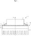
- Figure 1 illustrates a side view of an embodiment of a semiconductor power module 1 for a semiconductor device.
- the semiconductor power module 1 comprises a metal substrate structure 10, electronics 2 which is coupled with the metal substrate structure 10, and a heat sink 3 which is coupled with the metal substrate structure 10 as well.
- the electronics 2 can include chips, for example, and figure 1 is showing the semiconductor power module 1 with chips on the metal substrate structure 10.
- the electronics 2 are coupled with a metal top layer 11 and the heat sink 3 is coupled with a metal bottom layer 13 of the metal substrate structure 10.
- the metal substrate structure 10 further comprises a dielectric layer 12 formed between the metal top layer 11 and the metal bottom layer 13.
- Both, the metal top layer 11 and the metal bottom layer 13 consist of metal or at least comprise metal such as copper and/or aluminum, for example.
- Alternative thermally and/or electrically conductive materials or material combinations can be used instead.
- the dielectric layer 12 is pre-preg sheet or a molded epoxy with filler, for example.
- the filler can be ceramic like or realized by other inorganic filler like glass fibers.
- the dielectric layer 12 can comprise thermoplastic or thermosetting resin such as polyamide, PBT and/or PET.
- the dielectric layer 12 comprises a ceramic based insulation layer such as Al2O3, AlN, BN, Si3N4, SiO2.
- the dielectric layer 12 can also be based on other materials suitable for injection molding, transfer molding and/or compression molding such as bismaleimide, cyanate ester, polyimide and silicones, or might be even based on ceramic materials, such as hydroset materials.
- the metal substrate structure 10 realizes an insulated metal substrate with a structured topside metallization, a metal back side plate and a dielectric insulation layer in between. Pads of the metal top layer 11 are connected to components of the electronics 2 via leads 4 and/or via terminals 15 which are coupled with the metal top layer 11 by means of welding.
- the illustrated semiconductor power module 1 can realize a gel-filled power module, wherein the electronics 2 or even the whole top side or even more of the metal substrate structure 10 can be embedded in or covered by an epoxy and/or gel encapsulation. Such an encapsulation can be done by means of molding afterwards to the manufacturing of the metal substrate structure 10, for example.
- Options of preparation of the semiconductor power module 1 can comprise filling with a gel, filling with N epoxy resin like potting resin, transfer molding and/or other molding methods.
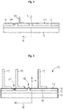
- FIG. 2-3 show two different embodiments of the metal substrate structure 10 in schematic side views.
- Figure 2 illustrates the metal substrate structure 10 comprising the metal top layer 11 including two penetrating recesses 14 which are filled with material of the dielectric layer 12 in a predetermined manner, formed by means of molding for example.
- the dielectric layer 12 is molded such that it extends into the recesses 14 and covers edges of the metal top layer 11 which limit the recesses 14, respectively.
- the one or more terminals 15 can be welded directly onto the metallization of the metal top layer 11 to form a direct conductive contact, for example.
- a respective contact surface 16 of a terminal 15 directly contacts the outer surface 111 of the metal top layer 11.
- a solder or another material such as a glue, a paint and/or a varnish layer can be located between the contact surface 16 of the terminal 15 and the outer surface 111 of the metal top layer 11 facing each other.
- soldering, sintering and/or gluing can be implemented in the manufacturing process.
- the terminals 15 are coupled with the metal top layer 11 by means of welding, for example by means of ultrasonic welding and/or laser welding. Other welding processes are possible as well.
- the coupling of the terminals 15 with the metal top layer 11 is done beforehand to a coupling of the metal top layer 11 with the dielectric layer 12 and/or the metal bottom layer 13.
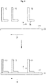
- the figures 4 to 6 illustrate different manufacturing states of a method for manufacturing an embodiment of the metal substrate structure 10 according to figure 3 , for example. Steps of the corresponding manufacturing method can follow the flow chart as shown in Figure 10 .
- a raw sheet 19 is provided to form the later metal top layer 11 (see upper part of figure 4 ).
- three terminals 15 are provided each comprising an L-shape with respect to a cross section spanned by the stacking direction A and a lateral direction B.
- different shapes of the terminals 15 are possible as well.
- a step S2 the terminals 15 are welded onto the outer surface 111 of the metal top layer 11 (see lower part of figure 4 ).
- the welding can be done in terms of ultrasonic welding and/or laser welding, for example.
- a step S3 the raw sheet 19 is stamped using a stamping tool with protrusions prepared to form recesses 14 and the metal top layer 11 with predetermined metallization structure, for example (see upper part of figure 5 ).
- separate metal pads can be stamped out beforehand to the welding of the terminals 15 onto the metal top layer 11 (see figure 7 ).
- Other methods of separation like etching, cutting or laser cutting are possible as well.
- the metal bottom layer 13 can be provided as well as a pumpable molding substance with predetermined material properties which realizes the liquid or viscous raw material to form the later dielectric layer 12. Moreover, in Step S4 the stamped metal top layer 11 with the welded terminals 15 on it and the provided metal bottom layer 13 are aligned relative to each other with a predetermined distance in between (see lower part of figure 5 ). This can be done by using a release film for fixation is a molding tool, for example, wherein the provided metallization structure of the metal top layer 11 is assembled onto. Afterwards, such a metal top layer release film unit can be positioned relatively to the provided metal bottom layer 13, for example, wherein the metal top layer 11 faces the metal bottom layer 13.
- a step S5 the provided molding substance is brought in into the free volume between the aligned metal top layer 11 and the metal bottom layer 13 and thereby molding of the dielectric layer 12 is processed.
- Formation of the dielectric layer 12 can be done by injection molding, transfer molding and/or compression molding and may include the formation of one or more ditches 17 and/or barriers 18 extending in and/or through a corresponding recess 14. For example, this is done by providing respective cavities limited by the molding tool and the metal top layer 11 in the region of the recesses 14. The provided substance is then brought into such cavities to form a trench, ditch 17, barrier 18 and/or rib.
- the molding tool has corresponding protrusions, for example.
- an embodiment of the metal substrate structure 10 for the semiconductor power module 1 can be manufactured consisting of a stamped metal plate topside realizing the metal top layer 11, an epoxy based molded insulation realizing the dielectric layer 12 and a metal plate bottom side realizing the metal bottom layer 13.
- etching of a homogeneous top metallization may be done after molding.
- Figure 7 illustrates an alternative step of providing the metal top layer 11 with predetermined penetrating recesses 14.
- the metal top layer 11 can be provided by means of stamping even before welding the terminals 15 to the metal top layer 11 (see upper part of figure 7 ). After welding the terminals 15 to the metal top layer 11 the manufacturing method can continue as illustrated in figure 5 and 6 .
- the figures 8 and 9 illustrate manufacturing states of a different method for manufacturing a further embodiment of the metal substrate structure 10.
- the metal substrate structure 10 can be formed by means of laminating, masking and etching.
- step S2 lamination is processed to couple the aforementioned layers 11, 12 and 13 together (see lower part of figure 8 ).
- a step S3 recesses 14 are formed in the metal top layer 11 due to masking and etching (see figure 9 ). Additionally, cleaning and/or levelling of the metal substrate structure 10 can be performed.
- the terminals 15 are joined to the metal top layer 11 before the coupling of the layers 11, 12, 13 of the metal substrate structure 10 is finished.
- the manufacturing of the metal substrate structure can realize a process within the manufacturing to the semiconductor power module 1.
- main and auxiliary terminals 15 are welded to a bare copper top side metallization plate realizing the metal top layer 11 beforehand to the manufacturing of the remaining metal substrate structure 10 itself. Consequently, no isolating resin sheet, which realizes the dielectric layer 12, is present and experiences mechanical and thermal stress during welding processing.
- the welding can be done by ultrasonic welding, laser welding, or any other type of applicable welding process.
- the welding process for the joining the terminals 15 is done before lamination or molding of the isolating material of the dielectric layer 12, respectively.
- a homogeneous copper top side plate with welded terminals 15, the pre-preg dielectric layer 12, and the bottom plate are coupled together.
- Circuit pattern are prepared by etching after the lamination process. Alternatively or additionally, a singulation of pattern can be done before lamination.
- the pattern of the circuit metallization can be prepared by stamping, etching and/or cutting before the injection, transfer or compression molding process is performed. Alternatively or additionally, a singulation of pattern can be done before lamination. Nevertheless, further process steps may be integrated into the manufacturing method as well, like cleaning processes or levelling processes for a top plate being deformed after the welding process before assembling of the complete insulated metal substrate structure 10.
- the terminals 15 can be made from copper or a copper alloy and can realize auxiliary or main terminals.
- a thickness of the terminals 15 can have a value of 0.2 mm up to 3.0 mm with respect to the lateral direction B and/or the stacking direction A. This may apply to both an upright body portion and/or a horizontal foot portion of the L-shaped terminal 15, respectively. Horizontal and vertical sections may have equal or different thicknesses.
Landscapes
- Engineering & Computer Science (AREA)
- Microelectronics & Electronic Packaging (AREA)
- Structures Or Materials For Encapsulating Or Coating Semiconductor Devices Or Solid State Devices (AREA)
- Cooling Or The Like Of Semiconductors Or Solid State Devices (AREA)
Abstract
Description
- The present disclosure is related to a metal substrate structure for a semiconductor power module and a semiconductor power module for a semiconductor device. The present disclosure is further related to a corresponding manufacturing method for a metal substrate structure.
- Conventional insulated metal substrates form technology for low and medium power semiconductor packages with low insulation requirements and low thermal resistance requirements simultaneously. Terminals are prepared on the insulated metal substrate.
- Embodiments of the present disclosure can provide a cost saving metal substrate structure for a semiconductor power module that enables reliable functioning even for high voltage power module applications. Further embodiments of the present disclosure can provide a corresponding semiconductor power module for a semiconductor device and a manufacturing method for such a metal substrate structure.
- According to an embodiment, a method for manufacturing a metal substrate structure for a semiconductor power module comprises providing at least one terminal, providing a metal top layer, providing a dielectric layer and providing a metal bottom layer. The method further comprises coupling the at least one terminal with the metal top layer by means of welding, for example by means of ultrasonic welding and/or laser welding. Other welding processes are possible as well. The method further comprises coupling the metal top layer with the dielectric layer and with the metal bottom layer such that the dielectric layer is coupled with both the metal top layer and the metal bottom layer in between, wherein the coupling of the at least one terminal with the metal top layer is done beforehand to the coupling of the metal top layer with the dielectric layer and the metal bottom layer.
- Due to the described manufacturing method realization of welded joining connections on an insulated metal substrate are possible which can contribute to a stable and reliable functioning of a semiconductor power module even for high voltage power module applications. The welding connection of the terminal and the metal top layer is done and then the metal top layer is coupled with the dielectric layer and/or the metal bottom layer. In other words, the coupling of the metal top layer with the dielectric layer and/or the metal bottom layer is processed afterwards to the coupling of the terminal with the metal top layer by means of welding. Thus, mechanical stress due to welding is kept away from the dielectric layer and contributes to avoid cracks or other damages of the dielectric layer.
- It is a recognition in connection with the present disclosure that conventional insulated metal substrates realize technologies for low and medium power semiconductor packages with low insulation requirements and low thermal resistance requirements simultaneously. For low reliability requirements, terminals can be e.g. soldered on substrate. Usually, welding provides better reliability, but a welding process can be critical for the substrate structure. In view of conventional setups of such insulated metal substrates corresponding terminals are connected to a top metallization using welding techniques to provide typically joining connections which can be critical with respect to a stable process on the substrates and a resin isolation sheet below the metallization. The welding process can lead to damages of the substrate structure and especially ultrasonic welding provides a strong impact of thermal and mechanical stress combined with heat on the substrate structure due to friction and pressure between a terminal foot and the substrate. Here a resin sheet is strongly endangered by deformation and crack formation. Corresponding failure modes must be considered when applying ultrasonic welding of terminal feet on a circuit metallization of an insulated metal substrate. Nevertheless, a high risk of a substrate damage is also available, if alternative welding methods would be used on such insulated metal substrates. Thus, a strong thermal impact must be considered as well, when joining terminal feet to substrates by laser welding, for example.
- Due to conventional manufacturing of such metal substrate structures, for example using ultrasonic welding, generation of severe damages in an isolating sheet of an insulating layer during the welding process can occur. After ultrasonic welding of main and/or auxiliary terminals on the circuit metallization of the top layer a complete delamination between the top layer and the isolating layer can occur. Deformation a resin sheet or isolating material can be further adhered to the delaminated metal sheet on the terminal positions resulting in the formation of conchoidal cracks also in the isolating sheet of an insulated metal substrate.
- By use of the described method for manufacturing a metal substrate structure it is possible to counteract the aforementioned adverse effects due to the separated welding process which is done beforehand and spaced apart from the coupling of the metal top layer and the dielectric layer. Thus, a risk of crack or damage formation can be completely suppressed and a stable semiconductor power module is feasible that enables reliable functioning even for high voltage power module applications in a voltage range of 0.5 kV up to 10.0 kV, for example. The one or more terminals can be welded directly onto a surface of the metal top layer to form a direct copper-to-copper contact, for example. Alternatively, solder or other materials such as a glue, a paint and/or varnish layer can be located between a bottom surface of the terminal and an upper surface of the metal top layer facing each other.
- According to an embodiment of the method the step of coupling the metal top layer with the dielectric layer and with the metal bottom layer comprises aligning the metal top layer, the dielectric layer and the metal bottom layer relative to each other. The method further comprises laminating the metal top layer, the dielectric layer and the metal bottom layer.
- Alternatively, the step of coupling the metal top layer with the dielectric layer and with the metal bottom layer comprises providing a molding substance, aligning the metal top layer and the metal bottom layer relative to each other with a predetermined distance in between, and then bringing in the provided molding substance between the aligned metal top layer and the metal bottom layer and thereby forming the dielectric layer by means of molding. The formation of the dielectric layer by means of molding can be done by injection molding, compression molding and/or transfer molding, for example.
- Thus, the dielectric layer can realize a pre-preg sheet which is assembled between two metal plates on top and the bottom forming the metal top layer and the metal bottom layer. Such metallization sheets or plates are bonded to the insulation of the dielectric layer by the lamination process, for example. A required metallization structure of the metal top layer can then be done by subsequent steps of masking and etching processes to locally remove conductive metal, creating the final metallization structure.
- With respect to a molded dielectric layer, the molding substance realizes a pumpable substance with predetermined material properties. The pumpable substance is a liquid or viscous raw material of the dielectric layer to be formed. For example, the molding substance is an epoxy and/or ceramic based liquid. Alternatively or additionally, the raw material of the dielectric layer may be a thermosetting or a thermoplastic resin material such as polyamide, PBT, PET. Alternatively or additionally, the raw material of the dielectric layer may comprise inorganic filler for improved thermal conductivity and/or CTE adjustment with respect to the metal top layer and/or the metal bottom layer. For example, the molded dielectric layer comprises a resin based dielectric material with ceramic filling material, e.g. epoxy, Al2O3, AlN, BN, Si3N4 or SiO2. For example, the dielectric layer is an epoxy with filler. The dielectric layer can be also based on other materials suitable for transfer, injection or compression molding such as bismaleimide, cyanate ester, polyimide and/or silicones. Alternatively or additionally, the dielectric layer can include a ceramic material and/or hydroset material or a material combination of two or more of the aforementioned components.
- The aligning of the metal top layer and the metal bottom layer relative to each other with a predetermined distance in between will substantially predetermine the later thickness of the molded dielectric layer. For example, the alignment can be realized by placing the metal top layer onto a release film or liner or another fixation, for example in a mold chase of a molding tool. This enables to precisely position the provided metallization structure of the metal top layer relative to the metal bottom layer and can be useful if the metal top layer comprises separate metal pads due to different potentials of operation, for example. In case of lamination, a thickness of a resin layer is given by the thickness and the behavior of the laminated layer.
- According to a further embodiment of the manufacturing method the metal top layer can be provided with at least one recess by means of stamping. In view of a stamped metal top layer, the coupling of the at least one terminal with the metal top layer by means of welding can done beforehand or subsequent to the stamping of the metal top layer.
- Alternatively or additionally, the metal top layer can be provided with at least one recess by means of etching and/or cutting, for example. Alternatively or additionally, the metal top layer is formed with a predetermined structure by means of laser cutting of a provided metal sheet, for example.
- The metallization of the metal top layer can be formed out of a film and/or a sheet comprising copper and/or aluminum and/or an alloy of copper and/or aluminum. This can also apply to the metal bottom layer which can be formed as a copper and/or aluminum plate, for example. The at least one recess can realize a penetrating opening through a coherent piece of metal forming the metallization of the metal top layer. Alternatively, the at least one recess forms a groove or a free volume between two separate metal paths, for example. The metal top layer can also comprise a plurality of recesses and/or grooves to form a predetermined metal pattern to prepare a desired metallization on the top of the metal substrate structure. This can also imply multiple separated metal pattern on a top surface of the metal substrate structure.
- The method of manufacturing the metal substrate structure can further comprise cleaning and/or levelling of the coupled terminal, the metal top layer, the dielectric layer and/or the metal bottom layer.
- Moreover, according to a further embodiment electronic is provided and coupled with the at least one terminal to form a semiconductor power module, for example.
- According to an embodiment, a metal substrate structure for a semiconductor power module comprises a metal top layer having at least one recess and at least one terminal which is coupled with the metal top layer by means of welding. The metal substrate structure further comprises a metal bottom layer and a dielectric layer which is coupled with both the metal top layer and the metal bottom layer and which is formed by means of molding between the metal top layer and the metal bottom layer. For example, the metal top layer including the at least one recess is formed by means of stamping and wherein the dielectric layer is molded such that it extends into the at least one recess. Additionally, the dielectric layer can be molded such that it forms a ditch or trench in the at least one recess. Alternatively, the dielectric layer is molded such that it forms an elevated portion or a barrier extending through the at least one recess protruding above an outer surface of the metal top layer.
- According to an embodiment, a semiconductor power module for a semiconductor device comprises an embodiment of the described metal substrate structure and electronics which is coupled with the at least one terminal of the metal substrate structure. The semiconductor power module can further comprise a heat sink which is coupled with the metal bottom layer of the metal substrate structure to dissipate heat during operation of the semiconductor power module. Thus, the semiconductor power module can comprise a separate heat sink. Alternatively or additionally, the metal bottom layer of the metal substrate structure can act as a heat sink itself and can be configured to comprise ribs or protrusion, for example, to provide a beneficial heat dissipation. The metal bottom layer can further act as a baseplate of the semiconductor power module. The semiconductor power module including the metal substrate structure can be further partly or completely encapsulated by resin prepared by molding or potting or dielectric gel. Terminals may act as power terminals or as auxiliary terminals, e.g. used for signal wiring.
- Moreover, the semiconductor power module can comprise two or more embodiments of the aforementioned metal substrate structure. The electronics may include chips, integrated circuits and/or other devices discrete devices.
- As a result of that the described method enables the manufacturing of embodiments of the aforementioned metal substrate structure and the semiconductor power module, described features and characteristics of the manufacturing method are also disclosed with respect to the metal substrate structure and the semiconductor power module and vice versa. Thus, the present disclosure comprises several aspects, wherein every feature described with respect to one of the aspects is also disclosed herein with respect to the other aspect, even if the respective feature is not explicitly mentioned in the context of the specific aspect.
- Exemplary embodiments are explained in the following with the aid of schematic drawings and reference numbers. The figures show:
- Figure 1
- embodiment of a semiconductor power module;
- Figures 2-3
- embodiments of a metal substrate structure for the semiconductor power module;
- Figures 4-7
- steps of manufacturing embodiments of the metal substrate structure for the semiconductor power module;
- Figures 8-9
- steps of manufacturing a further embodiment of the metal substrate structure for the semiconductor power module; and
- Figure 10
- flow chart for a method of manufacturing an embodiment of the metal substrate structure.
- The accompanying figures are included to provide a further understanding. It is to be understood that the embodiments shown in the figures are illustrative representations and are not necessarily drawn to scale. Identical reference numbers designate elements or components with identical functions. In so far as elements or components correspond to one another in terms of their function in different figures, the description thereof is not repeated for each of the following figures. For the sake of clarity elements might not appear with corresponding reference symbols in all figures possibly.
-
Figure 1 illustrates a side view of an embodiment of asemiconductor power module 1 for a semiconductor device. Thesemiconductor power module 1 comprises ametal substrate structure 10,electronics 2 which is coupled with themetal substrate structure 10, and aheat sink 3 which is coupled with themetal substrate structure 10 as well. Theelectronics 2 can include chips, for example, andfigure 1 is showing thesemiconductor power module 1 with chips on themetal substrate structure 10. With respect to an illustrated stacking direction A theelectronics 2 are coupled with ametal top layer 11 and theheat sink 3 is coupled with ametal bottom layer 13 of themetal substrate structure 10. Themetal substrate structure 10 further comprises adielectric layer 12 formed between themetal top layer 11 and themetal bottom layer 13. - Both, the
metal top layer 11 and themetal bottom layer 13 consist of metal or at least comprise metal such as copper and/or aluminum, for example. Alternative thermally and/or electrically conductive materials or material combinations can be used instead. Thedielectric layer 12 is pre-preg sheet or a molded epoxy with filler, for example. The filler can be ceramic like or realized by other inorganic filler like glass fibers. Alternatively or additionally, thedielectric layer 12 can comprise thermoplastic or thermosetting resin such as polyamide, PBT and/or PET. Alternatively or additionally, thedielectric layer 12 comprises a ceramic based insulation layer such as Al2O3, AlN, BN, Si3N4, SiO2. Thedielectric layer 12 can also be based on other materials suitable for injection molding, transfer molding and/or compression molding such as bismaleimide, cyanate ester, polyimide and silicones, or might be even based on ceramic materials, such as hydroset materials. Thus, themetal substrate structure 10 realizes an insulated metal substrate with a structured topside metallization, a metal back side plate and a dielectric insulation layer in between. Pads of themetal top layer 11 are connected to components of theelectronics 2 vialeads 4 and/or viaterminals 15 which are coupled with themetal top layer 11 by means of welding. - The illustrated
semiconductor power module 1 can realize a gel-filled power module, wherein theelectronics 2 or even the whole top side or even more of themetal substrate structure 10 can be embedded in or covered by an epoxy and/or gel encapsulation. Such an encapsulation can be done by means of molding afterwards to the manufacturing of themetal substrate structure 10, for example. Options of preparation of thesemiconductor power module 1 can comprise filling with a gel, filling with N epoxy resin like potting resin, transfer molding and/or other molding methods. - The
figures 2-3 show two different embodiments of themetal substrate structure 10 in schematic side views.Figure 2 illustrates themetal substrate structure 10 comprising themetal top layer 11 including two penetratingrecesses 14 which are filled with material of thedielectric layer 12 in a predetermined manner, formed by means of molding for example. Thus, thedielectric layer 12 is molded such that it extends into therecesses 14 and covers edges of themetal top layer 11 which limit therecesses 14, respectively. - According to the embodiment shown in
figure 3 , thedielectric layer 12 can be molded such that there is adielectric ditch 17 formed in onerecess 14 and adielectric barrier 18 formed in theother recess 14. Thebarrier 16 extends through the correspondingrecess 14 and protrudes above anouter surface 111 of themetal top layer 11. The protrusion of thebarrier 16 can be named as a rib. Theditch 15 and thebarrier 16 are integrally formed with thedielectric layer 12 in one molding process for example and their limiting dielectric material can cover edges of themetal top layer 11 which limit the corresponding recesses 14. - The one or
more terminals 15 can be welded directly onto the metallization of themetal top layer 11 to form a direct conductive contact, for example. Thus, arespective contact surface 16 of a terminal 15 directly contacts theouter surface 111 of themetal top layer 11. Alternatively, a solder or another material such as a glue, a paint and/or a varnish layer can be located between thecontact surface 16 of the terminal 15 and theouter surface 111 of themetal top layer 11 facing each other. In this respect, soldering, sintering and/or gluing can be implemented in the manufacturing process. - The
terminals 15 are coupled with themetal top layer 11 by means of welding, for example by means of ultrasonic welding and/or laser welding. Other welding processes are possible as well. The coupling of theterminals 15 with themetal top layer 11 is done beforehand to a coupling of themetal top layer 11 with thedielectric layer 12 and/or themetal bottom layer 13. - The
figures 4 to 6 illustrate different manufacturing states of a method for manufacturing an embodiment of themetal substrate structure 10 according tofigure 3 , for example. Steps of the corresponding manufacturing method can follow the flow chart as shown inFigure 10 . - In a step S1 a
raw sheet 19 is provided to form the later metal top layer 11 (see upper part offigure 4 ). Moreover, threeterminals 15 are provided each comprising an L-shape with respect to a cross section spanned by the stacking direction A and a lateral direction B. Of course, different shapes of theterminals 15 are possible as well. - In a step S2 the
terminals 15 are welded onto theouter surface 111 of the metal top layer 11 (see lower part offigure 4 ). The welding can be done in terms of ultrasonic welding and/or laser welding, for example. - In a step S3 the
raw sheet 19 is stamped using a stamping tool with protrusions prepared to formrecesses 14 and themetal top layer 11 with predetermined metallization structure, for example (see upper part offigure 5 ). - Alternatively, separate metal pads can be stamped out beforehand to the welding of the
terminals 15 onto the metal top layer 11 (seefigure 7 ). Other methods of separation like etching, cutting or laser cutting are possible as well. - In a step S4 the
metal bottom layer 13 can be provided as well as a pumpable molding substance with predetermined material properties which realizes the liquid or viscous raw material to form thelater dielectric layer 12. Moreover, in Step S4 the stampedmetal top layer 11 with the weldedterminals 15 on it and the providedmetal bottom layer 13 are aligned relative to each other with a predetermined distance in between (see lower part offigure 5 ). This can be done by using a release film for fixation is a molding tool, for example, wherein the provided metallization structure of themetal top layer 11 is assembled onto. Afterwards, such a metal top layer release film unit can be positioned relatively to the providedmetal bottom layer 13, for example, wherein themetal top layer 11 faces themetal bottom layer 13. - In a step S5 the provided molding substance is brought in into the free volume between the aligned
metal top layer 11 and themetal bottom layer 13 and thereby molding of thedielectric layer 12 is processed. Formation of thedielectric layer 12 can be done by injection molding, transfer molding and/or compression molding and may include the formation of one ormore ditches 17 and/orbarriers 18 extending in and/or through acorresponding recess 14. For example, this is done by providing respective cavities limited by the molding tool and themetal top layer 11 in the region of therecesses 14. The provided substance is then brought into such cavities to form a trench,ditch 17,barrier 18 and/or rib. For preparation of ditches, the molding tool has corresponding protrusions, for example. - Thus, an embodiment of the
metal substrate structure 10 for thesemiconductor power module 1 can be manufactured consisting of a stamped metal plate topside realizing themetal top layer 11, an epoxy based molded insulation realizing thedielectric layer 12 and a metal plate bottom side realizing themetal bottom layer 13. Alternatively, etching of a homogeneous top metallization may be done after molding. -
Figure 7 illustrates an alternative step of providing themetal top layer 11 with predetermined penetratingrecesses 14. Themetal top layer 11 can be provided by means of stamping even before welding theterminals 15 to the metal top layer 11 (see upper part offigure 7 ). After welding theterminals 15 to themetal top layer 11 the manufacturing method can continue as illustrated infigure 5 and6 . - The
figures 8 and9 illustrate manufacturing states of a different method for manufacturing a further embodiment of themetal substrate structure 10. According to such an embodiment themetal substrate structure 10 can be formed by means of laminating, masking and etching. - In a step S1 a
raw sheet 19 is provided to form the latermetal top layer 11 and theterminals 15 are welded to the outer surface 111 (see upper part offigure 8 ). Moreover, thedielectric layer 12 is provided in form of a pre-preg material sheet, for example. Moreover, themetal bottom layer 13 is provided and themetal top layer 11, thedielectric layer 12 and themetal bottom layer 13 are aligned with respect to each other. - In a step S2 lamination is processed to couple the
aforementioned layers figure 8 ). - In a step S3 recesses 14 are formed in the
metal top layer 11 due to masking and etching (seefigure 9 ). Additionally, cleaning and/or levelling of themetal substrate structure 10 can be performed. - According to the described embodiments the
terminals 15 are joined to themetal top layer 11 before the coupling of thelayers metal substrate structure 10 is finished. Here the manufacturing of the metal substrate structure can realize a process within the manufacturing to thesemiconductor power module 1. In contrast to conventional manufacturing processes for insulated metal substrates and subsequent module assembly processes, main andauxiliary terminals 15 are welded to a bare copper top side metallization plate realizing themetal top layer 11 beforehand to the manufacturing of the remainingmetal substrate structure 10 itself. Consequently, no isolating resin sheet, which realizes thedielectric layer 12, is present and experiences mechanical and thermal stress during welding processing. The welding can be done by ultrasonic welding, laser welding, or any other type of applicable welding process. - According to the illustrated process flows for the described possible setup types of the
metal substrate structure 10, the welding process for the joining theterminals 15 is done before lamination or molding of the isolating material of thedielectric layer 12, respectively. With respect of manufacturing themetal substrate structure 10 by means of a lamination process a homogeneous copper top side plate with weldedterminals 15, thepre-preg dielectric layer 12, and the bottom plate are coupled together. Circuit pattern are prepared by etching after the lamination process. Alternatively or additionally, a singulation of pattern can be done before lamination. - With respect of manufacturing the
metal substrate structure 10 by means of a molding process of the isolating material of thedielectric layer 12, the pattern of the circuit metallization can be prepared by stamping, etching and/or cutting before the injection, transfer or compression molding process is performed. Alternatively or additionally, a singulation of pattern can be done before lamination. Nevertheless, further process steps may be integrated into the manufacturing method as well, like cleaning processes or levelling processes for a top plate being deformed after the welding process before assembling of the complete insulatedmetal substrate structure 10. - The
terminals 15 can be made from copper or a copper alloy and can realize auxiliary or main terminals. A thickness of theterminals 15 can have a value of 0.2 mm up to 3.0 mm with respect to the lateral direction B and/or the stacking direction A. This may apply to both an upright body portion and/or a horizontal foot portion of the L-shapedterminal 15, respectively. Horizontal and vertical sections may have equal or different thicknesses. - Due to the described options of the manufacturing method it is possible to prevent a deformation of the comparably soft
resin dielectric layer 12 due to thermal and mechanical impact even when performing ultrasonic welding on the circuit metallization of themetal top layer 11. This further contributes to avoid at least local delamination between resin sheet and metal parts and/or crack formation inside the isolating sheet of the dielectric layer. Delamination or crack formation may also cause partial discharge and dielectric breakdown in high voltage power modules. Thus, there is no deformation of the resin sheet or modifications of the resin of thedielectric layer 12 visible caused by mechanical and/or thermal impact under the welded terminal feet. - Accordingly, a corresponding design of the
semiconductor power module 1 can comprise one or more of the following benefits: The proposed process flow circumvents the issue of possible damages on the mechanically and thermally sensitive resin isolating sheet of thedielectric layer 12 during the welding process. This opportunity makes the use of this comparably cost-effective substrate design interesting for large power modules and applicable for higher voltage classes, in view of novel joining methods like welding techniques (e.g. ultrasonic welding, laser welding) are used as well. Consequently, a significant cost-down may be possible, when replacing a conventional setup of substrates with ceramic isolating sheets soldered to a baseplate by an insulatedmetal substrate structure 10 according to the present disclosure. On one hand material costs may be reduced, and on the other hand several process steps like the joining process between themetal substrate structure 10 and a baseplate or cooler in thesemiconductor power module 1 can be removed from a corresponding process flow. - By use of the described method for manufacturing a metal substrate structure it is possible to counteract the formation of cracks or damages due to the separated welding process wherein the
terminals 15 are welded to circuit metallization of themetal top layer 11 before and space apart from the preparation of the insulatedmetal substrate structure 10 including the coupling of themetal top layer 11 and thedielectric layer 12. Thus, a risk of crack or damage formation is significantly reduced or even completely suppressed and a stablesemiconductor power module 1 is feasible that enables reliable functioning even for high voltage power module applications in a voltage range of 0.5 kV up to 10.0 kV, for example. - The embodiments shown in the
Figures 1 to 10 as stated represent exemplary embodiments of the improvedmetal substrate structure 10, thesemiconductor power module 1 and the manufacturing method for; therefore, they do not constitute a complete list of all embodiments. Actual arrangements and methods may vary from the embodiments shown in terms of metal substrate structures and power modules, for example. -
- 1
- semiconductor power module
- 2
- electronics
- 3
- heat sink
- 4
- leads
- 10
- metal substrate structure
- 11
- metal top layer
- 111
- outer surface
- 12
- dielectric layer
- 13
- metal bottom layer
- 14
- recess
- 15
- terminal
- 16
- contact surface
- 17
- molded ditch
- 18
- molded barrier
- 19
- raw sheet
- A
- stacking direction
- B
- lateral direction
- S(i)
- steps of a method for manufacturing a metal substrate structure for a semiconductor power module
Claims (15)
- A method for manufacturing a metal substrate structure (10) for a semiconductor power module (1), comprising:- providing at least one terminal (15),- providing a metal top layer (11),- providing a dielectric layer (12),- providing a metal bottom layer (13),- coupling the at least one terminal (15) with the metal top layer (11) by means of welding, and- coupling the metal top layer (11) with the dielectric layer (12) and with the metal bottom layer (13) such that the dielectric layer (12) is coupled with both the metal top layer (11) and the metal bottom layer (13) in between, wherein the coupling of the at least one terminal (15) with the metal top layer (11) is done beforehand to the coupling of the metal top layer (11) with the dielectric layer (12) and the metal bottom layer (13).
- The method according to claim 1, wherein the step of coupling the metal top layer (11) with the dielectric layer (12) and with the metal bottom layer (13) comprises:- aligning the metal top layer (11), the dielectric layer (12) and the metal bottom layer (13) relative to each other, and- laminating the metal top layer (11), the dielectric layer (12) and the metal bottom layer (13).
- The method according to claim 1, wherein the step of coupling the metal top layer (11) with the dielectric layer (12) and with the metal bottom layer (13) comprises:- providing a molding substance,- aligning the metal top layer (11) and the metal bottom layer (13) relative to each other with a predetermined distance in between, and- bringing in the provided molding substance between the aligned metal top layer (11) and the metal bottom layer (13) and thereby forming the dielectric layer (12) by means of molding.
- The method according to claim 3, wherein the dielectric layer (12) is formed by means of injection molding, compression molding and/or transfer molding.
- The method according to one of the preceding claims, wherein the step of providing the metal top layer (11) comprises:
Forming the metal top layer (11) with at least one recess (14) by means of masking and etching. - The method according to one of the preceding claims, wherein the step of providing the metal top layer (11) comprises:
Forming the metal top layer (11) with at least one recess (14) by means of stamping and/or cutting. - The method according to claim 6, wherein the coupling of the at least one terminal (15) with the metal top layer (11) by means of welding is done beforehand or subsequent to the stamping of the metal top layer (11).
- The method according one of the preceding claims, wherein the coupling of the at least one terminal (15) with the metal top layer (11) by means of welding is done by ultrasonic welding and/or laser welding.
- The method according to one of the preceding claims, further comprising:
Cleaning and/or levelling of the coupled at least one terminal (15), the metal top layer (11), the dielectric layer (12) and/or the metal bottom layer (13). - The method according to one of the preceding claims, further comprising:- providing electronics (2), and- coupling the electronics (2) with the metal top layer (11) .
- A metal substrate structure (10) for a semiconductor power module, comprising:- a metal top layer (11) having at least one recess (14),- at least one terminal (15) coupled with the metal top layer (11) by means of welding,- a metal bottom layer (13), and- a dielectric layer (12) which is coupled with both the metal top layer (11) and the metal bottom layer (13) and which is formed by means of molding between the metal top layer (11) and the metal bottom layer (13).
- The metal substrate structure (10) according to claim 11, wherein the metal top layer (11) including the at least one recess (14) is formed by means of stamping, etching and/or cutting and wherein the dielectric layer (12) is molded such that it extends into the at least one recess (14) .
- The metal substrate structure (10) according to claim 12, wherein the dielectric layer (12) is molded such that it forms at least one ditch (17) in the at least one recess (14) the metal top layer (11).
- The metal substrate structure (10) according to claim 12 or 13, wherein the dielectric layer (12) is molded such that it forms at least one barrier (18) extending through the at least one recess (14) protruding above an outer surface (111) of the metal top layer (11).
- A semiconductor power module (1) for a semiconductor device, comprising:- a metal substrate structure (10) according to one of the preceding claims, and- electronics (2) which is coupled with the metal top layer (11) of the metal substrate structure (10).
Priority Applications (4)
| Application Number | Priority Date | Filing Date | Title |
|---|---|---|---|
| EP21166412.3A EP4068348B1 (en) | 2021-03-31 | 2021-03-31 | Metal substrate structure and method of manufacturing a metal substrate structure for a semiconductor power module and semiconductor module |
| CN202210225822.4A CN115148607B (en) | 2021-03-31 | 2022-03-09 | Metal substrate structure for semiconductor power module and method for manufacturing the metal substrate structure and semiconductor power module |
| JP2022041548A JP7237214B2 (en) | 2021-03-31 | 2022-03-16 | METAL SUBSTRATE STRUCTURE FOR SEMICONDUCTOR POWER MODULE, METHOD FOR MANUFACTURING METAL SUBSTRATE STRUCTURE AND SEMICONDUCTOR POWER MODULE |
| US17/705,980 US12218192B2 (en) | 2021-03-31 | 2022-03-28 | Metal substrate structure for a semiconductor power module |
Applications Claiming Priority (1)
| Application Number | Priority Date | Filing Date | Title |
|---|---|---|---|
| EP21166412.3A EP4068348B1 (en) | 2021-03-31 | 2021-03-31 | Metal substrate structure and method of manufacturing a metal substrate structure for a semiconductor power module and semiconductor module |
Publications (2)
| Publication Number | Publication Date |
|---|---|
| EP4068348A1 true EP4068348A1 (en) | 2022-10-05 |
| EP4068348B1 EP4068348B1 (en) | 2023-11-29 |
Family
ID=75362350
Family Applications (1)
| Application Number | Title | Priority Date | Filing Date |
|---|---|---|---|
| EP21166412.3A Active EP4068348B1 (en) | 2021-03-31 | 2021-03-31 | Metal substrate structure and method of manufacturing a metal substrate structure for a semiconductor power module and semiconductor module |
Country Status (4)
| Country | Link |
|---|---|
| US (1) | US12218192B2 (en) |
| EP (1) | EP4068348B1 (en) |
| JP (1) | JP7237214B2 (en) |
| CN (1) | CN115148607B (en) |
Families Citing this family (1)
| Publication number | Priority date | Publication date | Assignee | Title |
|---|---|---|---|---|
| CN115885378B (en) * | 2020-09-17 | 2025-09-05 | 株式会社村田制作所 | High frequency module and communication device |
Citations (3)
| Publication number | Priority date | Publication date | Assignee | Title |
|---|---|---|---|---|
| EP1160861A2 (en) * | 2000-06-01 | 2001-12-05 | Matsushita Electric Industrial Co., Ltd. | Thermally conductive substrate with leadframe and heat radiation plate and manufacturing method thereof |
| EP1931183A2 (en) * | 2006-12-04 | 2008-06-11 | Hitachi, Ltd. | Electronic device |
| US20100201002A1 (en) * | 2007-07-17 | 2010-08-12 | Mitsubishi Electric Corporation | Semiconductor device and process for producing same |
Family Cites Families (21)
| Publication number | Priority date | Publication date | Assignee | Title |
|---|---|---|---|---|
| JP2003198077A (en) | 2001-12-26 | 2003-07-11 | Kyocera Corp | Ceramic circuit board |
| JP2003264354A (en) | 2002-03-11 | 2003-09-19 | Mitsubishi Electric Corp | Air conditioner control board |
| JP4057407B2 (en) | 2002-12-12 | 2008-03-05 | 三菱電機株式会社 | Semiconductor power module |
| JP5134582B2 (en) | 2009-02-13 | 2013-01-30 | 日立オートモティブシステムズ株式会社 | Connection structure and power module |
| KR20130051498A (en) * | 2010-10-13 | 2013-05-20 | 에이비비 리써치 리미티드 | Semiconductor module and method of manufacturing a semiconductor module |
| FR2969899B1 (en) | 2010-12-23 | 2012-12-21 | Valeo Sys Controle Moteur Sas | PRINTED CIRCUIT WITH INSULATED METAL SUBSTRATE |
| JP2012151198A (en) | 2011-01-18 | 2012-08-09 | Toyota Motor Corp | Structure for jointing bus bar and wiring |
| US8563364B2 (en) * | 2011-09-29 | 2013-10-22 | Infineon Technologies Ag | Method for producing a power semiconductor arrangement |
| WO2014080476A1 (en) * | 2012-11-21 | 2014-05-30 | 三菱電機株式会社 | Semiconductor device and method for producing same |
| JP6143884B2 (en) * | 2013-11-26 | 2017-06-07 | 三菱電機株式会社 | Power module |
| JP6091443B2 (en) * | 2014-01-31 | 2017-03-08 | 三菱電機株式会社 | Semiconductor module |
| CN104779220A (en) | 2015-03-27 | 2015-07-15 | 矽力杰半导体技术(杭州)有限公司 | Chip packaging structure and manufacture method thereof |
| JP6538513B2 (en) | 2015-10-02 | 2019-07-03 | 株式会社 日立パワーデバイス | Semiconductor power module and moving body |
| WO2017144599A1 (en) * | 2016-02-24 | 2017-08-31 | Abb Schweiz Ag | Power module based on multi-layer circuit board |
| JP6665664B2 (en) * | 2016-04-27 | 2020-03-13 | 富士電機株式会社 | Semiconductor device and manufacturing method thereof |
| JP7026451B2 (en) | 2017-05-11 | 2022-02-28 | 三菱電機株式会社 | Power semiconductor modules, their manufacturing methods, and power converters |
| JP7233407B2 (en) | 2017-07-10 | 2023-03-06 | ヒタチ・エナジー・スウィツァーランド・アクチェンゲゼルシャフト | Power semiconductor module containing dimples in the metallization layer below the legs of the terminals |
| JP6969471B2 (en) | 2018-03-23 | 2021-11-24 | 三菱マテリアル株式会社 | Insulated circuit board |
| EP3736854A1 (en) * | 2019-05-06 | 2020-11-11 | Infineon Technologies AG | Power semiconductor module arrangement |
| JP7001186B1 (en) | 2021-03-18 | 2022-01-19 | 富士電機株式会社 | Manufacturing methods for semiconductor devices, semiconductor modules, vehicles, and semiconductor devices |
| US20220310409A1 (en) * | 2021-03-24 | 2022-09-29 | Littelfuse, Inc. | Method to connect power terminal to substrate within semiconductor package |
-
2021
- 2021-03-31 EP EP21166412.3A patent/EP4068348B1/en active Active
-
2022
- 2022-03-09 CN CN202210225822.4A patent/CN115148607B/en active Active
- 2022-03-16 JP JP2022041548A patent/JP7237214B2/en active Active
- 2022-03-28 US US17/705,980 patent/US12218192B2/en active Active
Patent Citations (3)
| Publication number | Priority date | Publication date | Assignee | Title |
|---|---|---|---|---|
| EP1160861A2 (en) * | 2000-06-01 | 2001-12-05 | Matsushita Electric Industrial Co., Ltd. | Thermally conductive substrate with leadframe and heat radiation plate and manufacturing method thereof |
| EP1931183A2 (en) * | 2006-12-04 | 2008-06-11 | Hitachi, Ltd. | Electronic device |
| US20100201002A1 (en) * | 2007-07-17 | 2010-08-12 | Mitsubishi Electric Corporation | Semiconductor device and process for producing same |
Also Published As
| Publication number | Publication date |
|---|---|
| US20220344456A1 (en) | 2022-10-27 |
| EP4068348B1 (en) | 2023-11-29 |
| JP2022159012A (en) | 2022-10-17 |
| CN115148607B (en) | 2025-01-07 |
| JP7237214B2 (en) | 2023-03-10 |
| CN115148607A (en) | 2022-10-04 |
| US12218192B2 (en) | 2025-02-04 |
Similar Documents
| Publication | Publication Date | Title |
|---|---|---|
| US9978720B2 (en) | Insulated die | |
| CN110517991B (en) | Metal-ceramic module and manufacturing method thereof, circuit board module and manufacturing method thereof | |
| CN104900782B (en) | Manufacturing method of heat dissipation gain type circuit board with isolating piece | |
| EP2779230A2 (en) | Power overlay structure and method of making same | |
| KR20140113451A (en) | Power overlay structure and method of making same | |
| US10420204B2 (en) | Wiring board having electrical isolator and moisture inhibiting cap incorporated therein and method of making the same | |
| US20250174509A1 (en) | Encapsulated package with carrier, laminate body and component in between | |
| CN106571347A (en) | Insulated die | |
| EP2804209A1 (en) | Moulded electronics module | |
| US12218192B2 (en) | Metal substrate structure for a semiconductor power module | |
| EP4239660A1 (en) | Method of attaching a terminal to a metal substrate structure for a semiconductor power module and semiconductor power module | |
| JP7675197B2 (en) | Metal substrate structure, method for manufacturing metal substrate structure for semiconductor power module, and semiconductor power module | |
| CN108235559A (en) | Circuit board with spacer and bridge and its making process | |
| EP4283662A1 (en) | Method of attaching a terminal to a metal substrate structure for a semiconductor power module and semiconductor power module | |
| EP4292129B1 (en) | Semiconductor power module and method for manufacturing a semiconductor power module | |
| EP4080551A1 (en) | Semiconductor power module and method for manufacturing a semiconductor power module and semiconductor power device | |
| EP4057338B1 (en) | Metal substrate structure and method of manufacturing a metal substrate structure for a semiconductor power module and semiconductor power module | |
| JP7483595B2 (en) | Wiring board, electronic device, and method for manufacturing wiring board | |
| EP4187594A1 (en) | Metal substrate structure and method of attaching a terminal to a metal substrate structure for a semiconductor power module and semiconductor power module | |
| CN117352398A (en) | Multi-chip packaging method and multi-chip package |
Legal Events
| Date | Code | Title | Description |
|---|---|---|---|
| PUAI | Public reference made under article 153(3) epc to a published international application that has entered the european phase |
Free format text: ORIGINAL CODE: 0009012 |
|
| STAA | Information on the status of an ep patent application or granted ep patent |
Free format text: STATUS: REQUEST FOR EXAMINATION WAS MADE |
|
| 17P | Request for examination filed |
Effective date: 20220315 |
|
| AK | Designated contracting states |
Kind code of ref document: A1 Designated state(s): AL AT BE BG CH CY CZ DE DK EE ES FI FR GB GR HR HU IE IS IT LI LT LU LV MC MK MT NL NO PL PT RO RS SE SI SK SM TR |
|
| RIN1 | Information on inventor provided before grant (corrected) |
Inventor name: EHRBAR, ROMAN Inventor name: BEYER, HARALD Inventor name: GUILLON, DAVID |
|
| STAA | Information on the status of an ep patent application or granted ep patent |
Free format text: STATUS: EXAMINATION IS IN PROGRESS |
|
| 17Q | First examination report despatched |
Effective date: 20230316 |
|
| GRAP | Despatch of communication of intention to grant a patent |
Free format text: ORIGINAL CODE: EPIDOSNIGR1 |
|
| STAA | Information on the status of an ep patent application or granted ep patent |
Free format text: STATUS: GRANT OF PATENT IS INTENDED |
|
| P01 | Opt-out of the competence of the unified patent court (upc) registered |
Effective date: 20230527 |
|
| INTG | Intention to grant announced |
Effective date: 20230620 |
|
| GRAS | Grant fee paid |
Free format text: ORIGINAL CODE: EPIDOSNIGR3 |
|
| GRAA | (expected) grant |
Free format text: ORIGINAL CODE: 0009210 |
|
| STAA | Information on the status of an ep patent application or granted ep patent |
Free format text: STATUS: THE PATENT HAS BEEN GRANTED |
|
| AK | Designated contracting states |
Kind code of ref document: B1 Designated state(s): AL AT BE BG CH CY CZ DE DK EE ES FI FR GB GR HR HU IE IS IT LI LT LU LV MC MK MT NL NO PL PT RO RS SE SI SK SM TR |
|
| RAP1 | Party data changed (applicant data changed or rights of an application transferred) |
Owner name: HITACHI ENERGY LTD |
|
| REG | Reference to a national code |
Ref country code: GB Ref legal event code: FG4D |
|
| REG | Reference to a national code |
Ref country code: CH Ref legal event code: EP |
|
| REG | Reference to a national code |
Ref country code: DE Ref legal event code: R096 Ref document number: 602021007165 Country of ref document: DE |
|
| REG | Reference to a national code |
Ref country code: IE Ref legal event code: FG4D |
|
| REG | Reference to a national code |
Ref country code: LT Ref legal event code: MG9D |
|
| REG | Reference to a national code |
Ref country code: NL Ref legal event code: MP Effective date: 20231129 |
|
| PG25 | Lapsed in a contracting state [announced via postgrant information from national office to epo] |
Ref country code: GR Free format text: LAPSE BECAUSE OF FAILURE TO SUBMIT A TRANSLATION OF THE DESCRIPTION OR TO PAY THE FEE WITHIN THE PRESCRIBED TIME-LIMIT Effective date: 20240301 |
|
| PG25 | Lapsed in a contracting state [announced via postgrant information from national office to epo] |
Ref country code: IS Free format text: LAPSE BECAUSE OF FAILURE TO SUBMIT A TRANSLATION OF THE DESCRIPTION OR TO PAY THE FEE WITHIN THE PRESCRIBED TIME-LIMIT Effective date: 20240329 |
|
| PG25 | Lapsed in a contracting state [announced via postgrant information from national office to epo] |
Ref country code: LT Free format text: LAPSE BECAUSE OF FAILURE TO SUBMIT A TRANSLATION OF THE DESCRIPTION OR TO PAY THE FEE WITHIN THE PRESCRIBED TIME-LIMIT Effective date: 20231129 |
|
| PG25 | Lapsed in a contracting state [announced via postgrant information from national office to epo] |
Ref country code: ES Free format text: LAPSE BECAUSE OF FAILURE TO SUBMIT A TRANSLATION OF THE DESCRIPTION OR TO PAY THE FEE WITHIN THE PRESCRIBED TIME-LIMIT Effective date: 20231129 |
|
| PG25 | Lapsed in a contracting state [announced via postgrant information from national office to epo] |
Ref country code: LT Free format text: LAPSE BECAUSE OF FAILURE TO SUBMIT A TRANSLATION OF THE DESCRIPTION OR TO PAY THE FEE WITHIN THE PRESCRIBED TIME-LIMIT Effective date: 20231129 Ref country code: IS Free format text: LAPSE BECAUSE OF FAILURE TO SUBMIT A TRANSLATION OF THE DESCRIPTION OR TO PAY THE FEE WITHIN THE PRESCRIBED TIME-LIMIT Effective date: 20240329 Ref country code: GR Free format text: LAPSE BECAUSE OF FAILURE TO SUBMIT A TRANSLATION OF THE DESCRIPTION OR TO PAY THE FEE WITHIN THE PRESCRIBED TIME-LIMIT Effective date: 20240301 Ref country code: ES Free format text: LAPSE BECAUSE OF FAILURE TO SUBMIT A TRANSLATION OF THE DESCRIPTION OR TO PAY THE FEE WITHIN THE PRESCRIBED TIME-LIMIT Effective date: 20231129 Ref country code: BG Free format text: LAPSE BECAUSE OF FAILURE TO SUBMIT A TRANSLATION OF THE DESCRIPTION OR TO PAY THE FEE WITHIN THE PRESCRIBED TIME-LIMIT Effective date: 20240229 |
|
| REG | Reference to a national code |
Ref country code: AT Ref legal event code: MK05 Ref document number: 1637030 Country of ref document: AT Kind code of ref document: T Effective date: 20231129 |
|
| PG25 | Lapsed in a contracting state [announced via postgrant information from national office to epo] |
Ref country code: NL Free format text: LAPSE BECAUSE OF FAILURE TO SUBMIT A TRANSLATION OF THE DESCRIPTION OR TO PAY THE FEE WITHIN THE PRESCRIBED TIME-LIMIT Effective date: 20231129 |
|
| PG25 | Lapsed in a contracting state [announced via postgrant information from national office to epo] |
Ref country code: SE Free format text: LAPSE BECAUSE OF FAILURE TO SUBMIT A TRANSLATION OF THE DESCRIPTION OR TO PAY THE FEE WITHIN THE PRESCRIBED TIME-LIMIT Effective date: 20231129 Ref country code: RS Free format text: LAPSE BECAUSE OF FAILURE TO SUBMIT A TRANSLATION OF THE DESCRIPTION OR TO PAY THE FEE WITHIN THE PRESCRIBED TIME-LIMIT Effective date: 20231129 Ref country code: PL Free format text: LAPSE BECAUSE OF FAILURE TO SUBMIT A TRANSLATION OF THE DESCRIPTION OR TO PAY THE FEE WITHIN THE PRESCRIBED TIME-LIMIT Effective date: 20231129 Ref country code: NO Free format text: LAPSE BECAUSE OF FAILURE TO SUBMIT A TRANSLATION OF THE DESCRIPTION OR TO PAY THE FEE WITHIN THE PRESCRIBED TIME-LIMIT Effective date: 20240229 Ref country code: NL Free format text: LAPSE BECAUSE OF FAILURE TO SUBMIT A TRANSLATION OF THE DESCRIPTION OR TO PAY THE FEE WITHIN THE PRESCRIBED TIME-LIMIT Effective date: 20231129 Ref country code: LV Free format text: LAPSE BECAUSE OF FAILURE TO SUBMIT A TRANSLATION OF THE DESCRIPTION OR TO PAY THE FEE WITHIN THE PRESCRIBED TIME-LIMIT Effective date: 20231129 Ref country code: HR Free format text: LAPSE BECAUSE OF FAILURE TO SUBMIT A TRANSLATION OF THE DESCRIPTION OR TO PAY THE FEE WITHIN THE PRESCRIBED TIME-LIMIT Effective date: 20231129 |
|
| PG25 | Lapsed in a contracting state [announced via postgrant information from national office to epo] |
Ref country code: DK Free format text: LAPSE BECAUSE OF FAILURE TO SUBMIT A TRANSLATION OF THE DESCRIPTION OR TO PAY THE FEE WITHIN THE PRESCRIBED TIME-LIMIT Effective date: 20231129 |
|
| PG25 | Lapsed in a contracting state [announced via postgrant information from national office to epo] |
Ref country code: CZ Free format text: LAPSE BECAUSE OF FAILURE TO SUBMIT A TRANSLATION OF THE DESCRIPTION OR TO PAY THE FEE WITHIN THE PRESCRIBED TIME-LIMIT Effective date: 20231129 Ref country code: AT Free format text: LAPSE BECAUSE OF FAILURE TO SUBMIT A TRANSLATION OF THE DESCRIPTION OR TO PAY THE FEE WITHIN THE PRESCRIBED TIME-LIMIT Effective date: 20231129 |
|
| PG25 | Lapsed in a contracting state [announced via postgrant information from national office to epo] |
Ref country code: SK Free format text: LAPSE BECAUSE OF FAILURE TO SUBMIT A TRANSLATION OF THE DESCRIPTION OR TO PAY THE FEE WITHIN THE PRESCRIBED TIME-LIMIT Effective date: 20231129 |
|
| PG25 | Lapsed in a contracting state [announced via postgrant information from national office to epo] |
Ref country code: SM Free format text: LAPSE BECAUSE OF FAILURE TO SUBMIT A TRANSLATION OF THE DESCRIPTION OR TO PAY THE FEE WITHIN THE PRESCRIBED TIME-LIMIT Effective date: 20231129 Ref country code: SK Free format text: LAPSE BECAUSE OF FAILURE TO SUBMIT A TRANSLATION OF THE DESCRIPTION OR TO PAY THE FEE WITHIN THE PRESCRIBED TIME-LIMIT Effective date: 20231129 Ref country code: RO Free format text: LAPSE BECAUSE OF FAILURE TO SUBMIT A TRANSLATION OF THE DESCRIPTION OR TO PAY THE FEE WITHIN THE PRESCRIBED TIME-LIMIT Effective date: 20231129 Ref country code: IT Free format text: LAPSE BECAUSE OF FAILURE TO SUBMIT A TRANSLATION OF THE DESCRIPTION OR TO PAY THE FEE WITHIN THE PRESCRIBED TIME-LIMIT Effective date: 20231129 Ref country code: EE Free format text: LAPSE BECAUSE OF FAILURE TO SUBMIT A TRANSLATION OF THE DESCRIPTION OR TO PAY THE FEE WITHIN THE PRESCRIBED TIME-LIMIT Effective date: 20231129 Ref country code: DK Free format text: LAPSE BECAUSE OF FAILURE TO SUBMIT A TRANSLATION OF THE DESCRIPTION OR TO PAY THE FEE WITHIN THE PRESCRIBED TIME-LIMIT Effective date: 20231129 Ref country code: CZ Free format text: LAPSE BECAUSE OF FAILURE TO SUBMIT A TRANSLATION OF THE DESCRIPTION OR TO PAY THE FEE WITHIN THE PRESCRIBED TIME-LIMIT Effective date: 20231129 Ref country code: AT Free format text: LAPSE BECAUSE OF FAILURE TO SUBMIT A TRANSLATION OF THE DESCRIPTION OR TO PAY THE FEE WITHIN THE PRESCRIBED TIME-LIMIT Effective date: 20231129 |
|
| PG25 | Lapsed in a contracting state [announced via postgrant information from national office to epo] |
Ref country code: PT Free format text: LAPSE BECAUSE OF FAILURE TO SUBMIT A TRANSLATION OF THE DESCRIPTION OR TO PAY THE FEE WITHIN THE PRESCRIBED TIME-LIMIT Effective date: 20240401 |
|
| PG25 | Lapsed in a contracting state [announced via postgrant information from national office to epo] |
Ref country code: PT Free format text: LAPSE BECAUSE OF FAILURE TO SUBMIT A TRANSLATION OF THE DESCRIPTION OR TO PAY THE FEE WITHIN THE PRESCRIBED TIME-LIMIT Effective date: 20240401 |
|
| REG | Reference to a national code |
Ref country code: DE Ref legal event code: R097 Ref document number: 602021007165 Country of ref document: DE |
|
| PLBE | No opposition filed within time limit |
Free format text: ORIGINAL CODE: 0009261 |
|
| STAA | Information on the status of an ep patent application or granted ep patent |
Free format text: STATUS: NO OPPOSITION FILED WITHIN TIME LIMIT |
|
| PG25 | Lapsed in a contracting state [announced via postgrant information from national office to epo] |
Ref country code: SI Free format text: LAPSE BECAUSE OF FAILURE TO SUBMIT A TRANSLATION OF THE DESCRIPTION OR TO PAY THE FEE WITHIN THE PRESCRIBED TIME-LIMIT Effective date: 20231129 |
|
| PG25 | Lapsed in a contracting state [announced via postgrant information from national office to epo] |
Ref country code: SI Free format text: LAPSE BECAUSE OF FAILURE TO SUBMIT A TRANSLATION OF THE DESCRIPTION OR TO PAY THE FEE WITHIN THE PRESCRIBED TIME-LIMIT Effective date: 20231129 |
|
| REG | Reference to a national code |
Ref country code: CH Ref legal event code: PL |
|
| 26N | No opposition filed |
Effective date: 20240830 |
|
| PG25 | Lapsed in a contracting state [announced via postgrant information from national office to epo] |
Ref country code: LU Free format text: LAPSE BECAUSE OF NON-PAYMENT OF DUE FEES Effective date: 20240331 |
|
| PG25 | Lapsed in a contracting state [announced via postgrant information from national office to epo] |
Ref country code: MC Free format text: LAPSE BECAUSE OF FAILURE TO SUBMIT A TRANSLATION OF THE DESCRIPTION OR TO PAY THE FEE WITHIN THE PRESCRIBED TIME-LIMIT Effective date: 20231129 |
|
| PG25 | Lapsed in a contracting state [announced via postgrant information from national office to epo] |
Ref country code: MC Free format text: LAPSE BECAUSE OF FAILURE TO SUBMIT A TRANSLATION OF THE DESCRIPTION OR TO PAY THE FEE WITHIN THE PRESCRIBED TIME-LIMIT Effective date: 20231129 Ref country code: LU Free format text: LAPSE BECAUSE OF NON-PAYMENT OF DUE FEES Effective date: 20240331 |
|
| REG | Reference to a national code |
Ref country code: BE Ref legal event code: MM Effective date: 20240331 |
|
| PG25 | Lapsed in a contracting state [announced via postgrant information from national office to epo] |
Ref country code: BE Free format text: LAPSE BECAUSE OF NON-PAYMENT OF DUE FEES Effective date: 20240331 |
|
| PG25 | Lapsed in a contracting state [announced via postgrant information from national office to epo] |
Ref country code: FR Free format text: LAPSE BECAUSE OF NON-PAYMENT OF DUE FEES Effective date: 20240331 |
|
| PG25 | Lapsed in a contracting state [announced via postgrant information from national office to epo] |
Ref country code: IE Free format text: LAPSE BECAUSE OF NON-PAYMENT OF DUE FEES Effective date: 20240331 |
|
| PG25 | Lapsed in a contracting state [announced via postgrant information from national office to epo] |
Ref country code: IE Free format text: LAPSE BECAUSE OF NON-PAYMENT OF DUE FEES Effective date: 20240331 Ref country code: FR Free format text: LAPSE BECAUSE OF NON-PAYMENT OF DUE FEES Effective date: 20240331 Ref country code: BE Free format text: LAPSE BECAUSE OF NON-PAYMENT OF DUE FEES Effective date: 20240331 Ref country code: CH Free format text: LAPSE BECAUSE OF NON-PAYMENT OF DUE FEES Effective date: 20240331 |
|
| PG25 | Lapsed in a contracting state [announced via postgrant information from national office to epo] |
Ref country code: CY Free format text: LAPSE BECAUSE OF FAILURE TO SUBMIT A TRANSLATION OF THE DESCRIPTION OR TO PAY THE FEE WITHIN THE PRESCRIBED TIME-LIMIT; INVALID AB INITIO Effective date: 20210331 |
|
| PG25 | Lapsed in a contracting state [announced via postgrant information from national office to epo] |
Ref country code: HU Free format text: LAPSE BECAUSE OF FAILURE TO SUBMIT A TRANSLATION OF THE DESCRIPTION OR TO PAY THE FEE WITHIN THE PRESCRIBED TIME-LIMIT; INVALID AB INITIO Effective date: 20210331 |
|
| PG25 | Lapsed in a contracting state [announced via postgrant information from national office to epo] |
Ref country code: FI Free format text: LAPSE BECAUSE OF FAILURE TO SUBMIT A TRANSLATION OF THE DESCRIPTION OR TO PAY THE FEE WITHIN THE PRESCRIBED TIME-LIMIT Effective date: 20231129 |
|
| REG | Reference to a national code |
Ref country code: DE Ref legal event code: R079 Ref document number: 602021007165 Country of ref document: DE Free format text: PREVIOUS MAIN CLASS: H01L0023140000 Ipc: H10W0070690000 |
|
| PG25 | Lapsed in a contracting state [announced via postgrant information from national office to epo] |
Ref country code: TR Free format text: LAPSE BECAUSE OF FAILURE TO SUBMIT A TRANSLATION OF THE DESCRIPTION OR TO PAY THE FEE WITHIN THE PRESCRIBED TIME-LIMIT Effective date: 20231129 |
|
| PGFP | Annual fee paid to national office [announced via postgrant information from national office to epo] |
Ref country code: GB Payment date: 20260324 Year of fee payment: 6 |
|
| PGFP | Annual fee paid to national office [announced via postgrant information from national office to epo] |
Ref country code: DE Payment date: 20260319 Year of fee payment: 6 |