EP4068049A1 - Power supply system and method - Google Patents
Power supply system and method Download PDFInfo
- Publication number
- EP4068049A1 EP4068049A1 EP21187919.2A EP21187919A EP4068049A1 EP 4068049 A1 EP4068049 A1 EP 4068049A1 EP 21187919 A EP21187919 A EP 21187919A EP 4068049 A1 EP4068049 A1 EP 4068049A1
- Authority
- EP
- European Patent Office
- Prior art keywords
- power supply
- control chip
- supply control
- power
- detection device
- Prior art date
- Legal status (The legal status is an assumption and is not a legal conclusion. Google has not performed a legal analysis and makes no representation as to the accuracy of the status listed.)
- Granted
Links
Images


Classifications
-
- G—PHYSICS
- G06—COMPUTING OR CALCULATING; COUNTING
- G06F—ELECTRIC DIGITAL DATA PROCESSING
- G06F1/00—Details not covered by groups G06F3/00 - G06F13/00 and G06F21/00
- G06F1/24—Resetting means
-
- G—PHYSICS
- G05—CONTROLLING; REGULATING
- G05F—SYSTEMS FOR REGULATING ELECTRIC OR MAGNETIC VARIABLES
- G05F1/00—Automatic systems in which deviations of an electric quantity from one or more predetermined values are detected at the output of the system and fed back to a device within the system to restore the detected quantity to its predetermined value or values, i.e. retroactive systems
- G05F1/10—Regulating voltage or current
- G05F1/46—Regulating voltage or current wherein the variable actually regulated by the final control device is DC
- G05F1/56—Regulating voltage or current wherein the variable actually regulated by the final control device is DC using semiconductor devices in series with the load as final control devices
- G05F1/565—Regulating voltage or current wherein the variable actually regulated by the final control device is DC using semiconductor devices in series with the load as final control devices sensing a condition of the system or its load in addition to means responsive to deviations in the output of the system, e.g. current, voltage, power factor
- G05F1/569—Regulating voltage or current wherein the variable actually regulated by the final control device is DC using semiconductor devices in series with the load as final control devices sensing a condition of the system or its load in addition to means responsive to deviations in the output of the system, e.g. current, voltage, power factor for protection
-
- G—PHYSICS
- G05—CONTROLLING; REGULATING
- G05F—SYSTEMS FOR REGULATING ELECTRIC OR MAGNETIC VARIABLES
- G05F1/00—Automatic systems in which deviations of an electric quantity from one or more predetermined values are detected at the output of the system and fed back to a device within the system to restore the detected quantity to its predetermined value or values, i.e. retroactive systems
- G05F1/10—Regulating voltage or current
- G05F1/625—Regulating voltage or current wherein it is irrelevant whether the variable actually regulated is AC or DC
-
- G—PHYSICS
- G06—COMPUTING OR CALCULATING; COUNTING
- G06F—ELECTRIC DIGITAL DATA PROCESSING
- G06F1/00—Details not covered by groups G06F3/00 - G06F13/00 and G06F21/00
- G06F1/26—Power supply means, e.g. regulation thereof
- G06F1/28—Supervision thereof, e.g. detecting power-supply failure by out of limits supervision
-
- G—PHYSICS
- G06—COMPUTING OR CALCULATING; COUNTING
- G06F—ELECTRIC DIGITAL DATA PROCESSING
- G06F1/00—Details not covered by groups G06F3/00 - G06F13/00 and G06F21/00
- G06F1/26—Power supply means, e.g. regulation thereof
- G06F1/30—Means for acting in the event of power-supply failure or interruption, e.g. power-supply fluctuations
Definitions
- the present disclosure relates to a power supply system and method, and more particularly to a power supply system and method utilizing a detection device to control a power supply switch, thereby controlling the connection between the power supply device and the power supply control chip.
- USB socket with power supply function is placed within the reach of life, such as on the wall or on the center console of the car. Therefore, the users can charge mobile phones, tablets or other electronic products with compatible specifications at any time.
- the prior USB chips with power supply function are susceptible to noise interference such as static electricity.
- the USB chip When the USB chip is interfered, the internal firmware of the USB chip would be abnormal, and the power supply would be interrupted or unable to reach the ideal speed. Under this circumstance, the power source that supplies the USB chip needs to be turned off and then re-conducted, so that the power supply is restored and the USB chip is restarted.
- the side of receiving power is often located in an enclosed space.
- the side of receiving power of the USB socket on the wall is located inside the wall, or the side of receiving power of the USB socket on the car is located inside the car shell.
- the USB chip receives the power from the supply mains or the battery in the car.
- the power source powering the USB chip cannot be manually turned off because of being located in the enclosed space (e.g., the supply mains or the battery in the car). Thus, the USB chip cannot be restarted to restore normal power supply.
- the power supply switch controls the connection between the power supply device and the power supply control chip so that the power supply control chip is restarted and resumes normal supply of input power to the electronic device.
- the power supply system and method of the present disclosure utilizes the detection device to control the power supply switch to be turned on or off, so as to control the connection between the power supply device and the power supply control chip. Therefore, the present disclosure overcomes the shortcomings in the prior art that the power supply to the power supply control chip cannot be manually turned off and the power supply control chip cannot be restarted.
- the power supply system includes an output terminal, a power supply control chip, a power supply switch and a detection device.
- the output terminal has a power supplying side and a power receiving side, and the power supplying side is configured to provide an input power to an electronic device at the power receiving side.
- the power supply control chip is connected between the power supply device and the electronic device and is configured to adjust the amount of the input power provided to the electronic device by the power supply device.
- the power supply switch is connected between the power supply device and the power supply control chip and is configured to control the connection between the power supply device and the power supply control chip.
- the detection device is connected between the power supply control chip and the power supply switch and is configured to detect whether the power supply control chip operates normally.
- the detection device controls the connection between the power supply device and the power supply control chip through the power supply switch for restarting the power supply control chip.
- the power supply control chip, the power supply switch and the detection device are disposed at the power supplying side, and the power supplying side is disposed in an enclosed space.
- a power supply method including steps of: (a) providing a power supply control chip, a power supply switch and a detection device, wherein the power supply control chip, the power supply switch and the detection device are disposed in an enclosed space; (b) supplying power to the power supply control chip and the electronic device disposed outside the enclosed space by the power supply device; (c) detecting whether the power supply control chip operates normally by the detection device, performing a step (d) if the detection result is negative, and performing the step (c) again if the detection result is positive; (d) controlling the connection between the power supply device and the power supply control chip by the power supply switch; and (e) restarting the power supply control chip.
- FIG. 1 is a schematic circuit diagram illustrating a power supply system according to an embodiment of the present disclosure.
- the power supply system 1 includes an output terminal 2, a power supply control chip 3, a power supply switch 4 and a detection device 5.
- the output terminal 2 has a power supplying side 20 and a power receiving side 21, and the power supplying side 20 is opposite to the power receiving side 21.
- the power supplying side 20 is configured to provide an input power to an electronic device 7 at the power receiving side 21.
- the power supplying side 20 receives the input power and outputs the input power to the power receiving side 21, and the electronic device 7 at the power receiving side 21 operates normally due to receiving the input power.
- the power receiving side 21 has connector(s) like USB Type-A, USB Type-B, USB Type-C or other USB-supported connectors, but not exclusively, to correspond to the various possible connection interfaces of the electronic device 7.
- the power supply control chip 3 is connected between the power supply device 6 and the electronic device 7.
- the power supply control chip 3 is powered by the power supply device 6 and is configured to adjust the amount of the input power provided to the electronic device 7 by the power supply device 6.
- the power supply control chip 3 adjusts the power supply device 6 to provide the input power according to the input power actually required by the electronic device 7.
- the power supply device 6 is capable of converting AC power into DC power, but not limited thereto.
- the power supply switch 4 is connected between the power supply device 6 and the power supply control chip 3 and is configured to control the connection between the power supply device 6 and the power supply control chip 3.
- the detection device 5 is connected between the power supply control chip 3 and the power supply switch 4 and is configured to detect whether the power supply control chip 3 operates normally. When the power supply control chip 3 operates abnormally, the detection device 5 controls the connection between the power supply device 6 and the power supply control chip 3 through the power supply switch 4 for restarting the power supply control chip 3. In an embodiment, when the detection device 5 detects that the power supply control chip 3 operates abnormally, the detection device 5 controls the power supply switch 4 to be in an off state so as to disconnect the connection between the power supply device 6 and the power supply control chip 3. Accordingly, the power supply device 6 cannot supply power to the power supply control chip 3, and the power supply control chip 3 stops operating.
- the detection device 5 controls the power supply switch 4 to be in an on state so as to reconnect the power supply device 6 to the power supply control chip 3. Accordingly, the power supply device 6 supplies power to the power supply control chip 3, and the power supply control chip 3 is restarted.
- the length of the waiting time is 1 second in some embodiments but not limited thereto, the length of the waiting time can be adjusted according to actual needs.
- the power supply control chip 3, the power supply switch 4 and the detection device 5 are disposed at the power supplying side 20, and the power supplying side 20 is disposed in an enclosed space 9.
- the output terminal 2 is disposed on the wall 8, the power supplying side 20 and the power receiving side 21 are located at two sides of the wall 8 respectively, and the enclosed space 9 is located at the side of the wall 8 where the socket receives the power (i.e., at the same side as the power supply device 6).
- the power supply system 1 of the present disclosure utilizes the detection device 5 to control the power supply switch 4 to be turned off or on, so as to control the connection between the power supply device 6 and the power supply control chip 3. Therefore, the present disclosure overcomes the shortcomings in the prior art that the power supply to the power supply control chip cannot be manually turned off and the power supply control chip cannot be restarted
- the detection device 5 is for example but not limited to micro controller unit, micro processor or detection circuit.
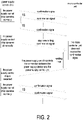
- the detection device 5 is a micro controller unit, and how the micro controller unit detects whether the power supply control chip 3 operates normally and restarts the power supply control chip 3 when the operation is abnormal is exemplified as follows. As shown in FIG. 2 , when the power supply control chip 3 operates normally, the power supply control chip 3 sends a confirmation signal to the micro controller unit regularly, and the period of sending the confirmation signal is for example but not limited to 1 second. When the power supply control chip 3 operates abnormally, the power supply control chip 3 stops sending the confirmation signal to the micro controller unit.
- the micro controller unit If the micro controller unit does not receive the confirmation signal within a waiting time, the micro controller unit controls the power supply switch 4 to control the connection between the power supply device 6 and the power supply control chip 3. Thereby, the power supply control chip 3 is restarted, and the power supply control chip 3 thus resumes normal operation.
- the length of the waiting time is 1 second in some embodiments but not limited thereto, the length of the waiting time can be adjusted according to actual needs.
- the detection device 5 being a detection circuit 50 is exemplified as follow.
- the detection circuit 50 includes a comparator 51 and a switch 52.
- the power supply device 6 provides a power supply voltage Vcc to the power supply control chip 3.
- the detection circuit 50 utilizes the comparator 51 to compare the working voltage Vo of the power supply control chip 3 with the reference voltage Vref. When the working voltage Vo of the power supply control chip 3 is greater than the reference voltage Vref, it means that the power supply control chip 3 operates normally. Under this circumstance, the switch 52 is turned off, the power supply switch 4 is turned on, and the power supply device 6 keeps supplying power to the power supply control chip 3.
- the switch 52 When the working voltage Vo of the power supply control chip 3 is less than the reference voltage Vref, it means that the power supply control chip 3 operates abnormally. Under this circumstance, the switch 52 is turned on, the power supply switch 4 is turned off, the power supply device 6 cannot supply power to the power supply control chip 3, and thus the power supply control chip 3 stops operation. After a waiting time, the switch 52 is turned off and the power supply switch 4 is turned on to reconnect the power supply device 6 to the power supply control chip 3. Accordingly, the power supply device 6 supplies power to the power supply control chip 3, and the power supply control chip 3 is restarted.
- the detection circuit 50 in this embodiment utilizes the comparator 51 to compare the working voltage Vo of the power supply control chip 3 with the reference voltage Vref, thereby determining whether the power supply control chip 3 operates normally.
- the reference voltage Vref is for example not limited to 2.5V, and the value of the reference voltage Vref can be adjusted according to the power supply speed requirements or the protocol specifications of the power supply control chip.
- the power supply control chip 3 is a power supply control chip with a fast power supply function
- the fast charge protocol supported by the power supply control chip is for example but not limited to the Power Delivery protocol (PD), the Quick Charge protocol (QC), etc.
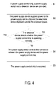
- FIG. 4 is a flow chart illustrating a power supply method according to an embodiment of the present disclosure.
- the power supply method of the present disclosure is applicable for the power supply system 1 stated above.
- the power supply method includes steps S1, S2, S3, S4 and S5.
- step S1 a power supply control chip 3, a power supply switch 4 and a detection device 5 are provided.
- the power supply control chip 3, the power supply switch 4 and the detection device 5 are disposed at a power supplying side 20, and the power supplying side 20 is disposed in an enclosed space 9.
- the power supply device 6 supplies power to the power supply control chip 3 and the electronic device 7 disposed outside the enclosed space 9.
- the detection device detects whether the power supply control chip 3 operates normally.
- step S4 is performed if the detection result is negative, and the step S3 is performed again if the detection result is positive.
- the power supply switch 4 controls the connection between the power supply device 6 and the power supply control chip 3.
- step S5 the power supply control chip 3 is restarted.
- step S3 the detection device 5 is a micro controller unit.
- the power supply control chip 3 When the power supply control chip 3 operates normally, the power supply control chip 3 sends a confirmation signal to the micro controller unit, and step S3 is performed again.
- the power supply control chip When the power supply control chip operates abnormally, the power supply control chip 3 stops sending the confirmation signal to the micro controller unit. If the micro controller unit does not receive the confirmation signal within a waiting time, step S4 is performed.
- step S3 the detection device 5 is a detection circuit 50.
- step S3 is performed again.
- step S4 is performed.
- the present disclosure provides a power supply device and method, the detection device of which regularly detects whether the power supply control chip operates normally.
- the power supply switch controls the connection between the power supply device and the power supply control chip so that the power supply control chip is restarted and resumes normal supply of input power to the electronic device.
- the power supply system and method of the present disclosure utilizes the detection device to control the power supply switch to be turned on or off , so as to control the connection between the power supply device and the power supply control chip. Therefore, the present disclosure overcomes the shortcomings in the prior art that the power supply to the power supply control chip cannot be manually turned off and the power supply control chip cannot be restarted.
Landscapes
- Engineering & Computer Science (AREA)
- Theoretical Computer Science (AREA)
- Physics & Mathematics (AREA)
- General Physics & Mathematics (AREA)
- General Engineering & Computer Science (AREA)
- Electromagnetism (AREA)
- Radar, Positioning & Navigation (AREA)
- Automation & Control Theory (AREA)
- Power Engineering (AREA)
- Direct Current Feeding And Distribution (AREA)
- Power Sources (AREA)
Abstract
Description
- The present disclosure relates to a power supply system and method, and more particularly to a power supply system and method utilizing a detection device to control a power supply switch, thereby controlling the connection between the power supply device and the power supply control chip.
- In order to meet the power supply needs of a large number of electronic products, the USB socket with power supply function is placed within the reach of life, such as on the wall or on the center console of the car. Therefore, the users can charge mobile phones, tablets or other electronic products with compatible specifications at any time.
- The prior USB chips with power supply function are susceptible to noise interference such as static electricity. When the USB chip is interfered, the internal firmware of the USB chip would be abnormal, and the power supply would be interrupted or unable to reach the ideal speed. Under this circumstance, the power source that supplies the USB chip needs to be turned off and then re-conducted, so that the power supply is restored and the USB chip is restarted. However, in a USB socket, the side of receiving power is often located in an enclosed space. For example, the side of receiving power of the USB socket on the wall is located inside the wall, or the side of receiving power of the USB socket on the car is located inside the car shell. Further, the USB chip receives the power from the supply mains or the battery in the car. Therefore, when the USB chip operates abnormally, the power source powering the USB chip cannot be manually turned off because of being located in the enclosed space (e.g., the supply mains or the battery in the car). Thus, the USB chip cannot be restarted to restore normal power supply.
- Therefore, there is a need of providing a power supply system and method to obviate the drawbacks encountered from the prior arts.
- It is an object of the present disclosure to provide a power supply system and method, the detection device of which regularly detects whether the power supply control chip operates normally. When the power supply control chip operates abnormally, the power supply switch controls the connection between the power supply device and the power supply control chip so that the power supply control chip is restarted and resumes normal supply of input power to the electronic device. The power supply system and method of the present disclosure utilizes the detection device to control the power supply switch to be turned on or off, so as to control the connection between the power supply device and the power supply control chip. Therefore, the present disclosure overcomes the shortcomings in the prior art that the power supply to the power supply control chip cannot be manually turned off and the power supply control chip cannot be restarted.
- In accordance with an aspect of the present disclosure, there is provided a power supply system. The power supply system includes an output terminal, a power supply control chip, a power supply switch and a detection device. The output terminal has a power supplying side and a power receiving side, and the power supplying side is configured to provide an input power to an electronic device at the power receiving side. The power supply control chip is connected between the power supply device and the electronic device and is configured to adjust the amount of the input power provided to the electronic device by the power supply device. The power supply switch is connected between the power supply device and the power supply control chip and is configured to control the connection between the power supply device and the power supply control chip. The detection device is connected between the power supply control chip and the power supply switch and is configured to detect whether the power supply control chip operates normally. When the power supply control chip operates abnormally, the detection device controls the connection between the power supply device and the power supply control chip through the power supply switch for restarting the power supply control chip. The power supply control chip, the power supply switch and the detection device are disposed at the power supplying side, and the power supplying side is disposed in an enclosed space.
- In accordance with an aspect of the present disclosure, there is provided a power supply method. The power supply method including steps of: (a) providing a power supply control chip, a power supply switch and a detection device, wherein the power supply control chip, the power supply switch and the detection device are disposed in an enclosed space; (b) supplying power to the power supply control chip and the electronic device disposed outside the enclosed space by the power supply device; (c) detecting whether the power supply control chip operates normally by the detection device, performing a step (d) if the detection result is negative, and performing the step (c) again if the detection result is positive; (d) controlling the connection between the power supply device and the power supply control chip by the power supply switch; and (e) restarting the power supply control chip.
- The above contents of the present invention will become more readily apparent to those ordinarily skilled in the art after reviewing the following detailed description and accompanying drawings, in which:
-
-
FIG. 1 is a schematic circuit diagram illustrating a power supply system according to an embodiment of the present disclosure; -
FIG. 2 is a schematic diagram illustrating the signal transmission between the power supply control chip and the micro controller unit according to another embodiment of the present disclosure; -
FIG. 3 is a schematic circuit diagram illustrating the detecting circuit according to another embodiment of the present disclosure; and -
FIG. 4 is a flow chart illustrating a power supply method according to an embodiment of the present disclosure. - The present disclosure will now be described more specifically with reference to the following embodiments. It is to be noted that the following descriptions of preferred embodiments of this disclosure are presented herein for purpose of illustration and description only. It is not intended to be exhaustive or to be limited to the precise form disclosed.
-
FIG. 1 is a schematic circuit diagram illustrating a power supply system according to an embodiment of the present disclosure. As shown inFIG. 1 , thepower supply system 1 includes anoutput terminal 2, a powersupply control chip 3, apower supply switch 4 and adetection device 5. Theoutput terminal 2 has a power supplying side 20 and apower receiving side 21, and the power supplying side 20 is opposite to thepower receiving side 21. The power supplying side 20 is configured to provide an input power to anelectronic device 7 at thepower receiving side 21. Specifically, the power supplying side 20 receives the input power and outputs the input power to thepower receiving side 21, and theelectronic device 7 at thepower receiving side 21 operates normally due to receiving the input power. In an embodiment, thepower receiving side 21 has connector(s) like USB Type-A, USB Type-B, USB Type-C or other USB-supported connectors, but not exclusively, to correspond to the various possible connection interfaces of theelectronic device 7. The powersupply control chip 3 is connected between thepower supply device 6 and theelectronic device 7. The powersupply control chip 3 is powered by thepower supply device 6 and is configured to adjust the amount of the input power provided to theelectronic device 7 by thepower supply device 6. Specifically, the powersupply control chip 3 adjusts thepower supply device 6 to provide the input power according to the input power actually required by theelectronic device 7. In an embodiment, thepower supply device 6 is capable of converting AC power into DC power, but not limited thereto. Thepower supply switch 4 is connected between thepower supply device 6 and the powersupply control chip 3 and is configured to control the connection between thepower supply device 6 and the powersupply control chip 3. - The
detection device 5 is connected between the powersupply control chip 3 and thepower supply switch 4 and is configured to detect whether the powersupply control chip 3 operates normally. When the powersupply control chip 3 operates abnormally, thedetection device 5 controls the connection between thepower supply device 6 and the powersupply control chip 3 through thepower supply switch 4 for restarting the powersupply control chip 3. In an embodiment, when thedetection device 5 detects that the powersupply control chip 3 operates abnormally, thedetection device 5 controls thepower supply switch 4 to be in an off state so as to disconnect the connection between thepower supply device 6 and the powersupply control chip 3. Accordingly, thepower supply device 6 cannot supply power to the powersupply control chip 3, and the powersupply control chip 3 stops operating. After a waiting time, thedetection device 5 controls thepower supply switch 4 to be in an on state so as to reconnect thepower supply device 6 to the powersupply control chip 3. Accordingly, thepower supply device 6 supplies power to the powersupply control chip 3, and the powersupply control chip 3 is restarted. The length of the waiting time is 1 second in some embodiments but not limited thereto, the length of the waiting time can be adjusted according to actual needs. The powersupply control chip 3, thepower supply switch 4 and thedetection device 5 are disposed at the power supplying side 20, and the power supplying side 20 is disposed in an enclosedspace 9. - In an embodiment, the
output terminal 2 is disposed on thewall 8, the power supplying side 20 and thepower receiving side 21 are located at two sides of thewall 8 respectively, and the enclosedspace 9 is located at the side of thewall 8 where the socket receives the power (i.e., at the same side as the power supply device 6). Thepower supply system 1 of the present disclosure utilizes thedetection device 5 to control thepower supply switch 4 to be turned off or on, so as to control the connection between thepower supply device 6 and the powersupply control chip 3. Therefore, the present disclosure overcomes the shortcomings in the prior art that the power supply to the power supply control chip cannot be manually turned off and the power supply control chip cannot be restarted - In an embodiment, the
detection device 5 is for example but not limited to micro controller unit, micro processor or detection circuit. For example, thedetection device 5 is a micro controller unit, and how the micro controller unit detects whether the powersupply control chip 3 operates normally and restarts the powersupply control chip 3 when the operation is abnormal is exemplified as follows. As shown inFIG. 2 , when the powersupply control chip 3 operates normally, the powersupply control chip 3 sends a confirmation signal to the micro controller unit regularly, and the period of sending the confirmation signal is for example but not limited to 1 second. When the powersupply control chip 3 operates abnormally, the powersupply control chip 3 stops sending the confirmation signal to the micro controller unit. If the micro controller unit does not receive the confirmation signal within a waiting time, the micro controller unit controls thepower supply switch 4 to control the connection between thepower supply device 6 and the powersupply control chip 3. Thereby, the powersupply control chip 3 is restarted, and the powersupply control chip 3 thus resumes normal operation. The length of the waiting time is 1 second in some embodiments but not limited thereto, the length of the waiting time can be adjusted according to actual needs. - The implementation of the
detection device 5 being adetection circuit 50 is exemplified as follow. As shown inFIG. 3 , thedetection circuit 50 includes acomparator 51 and aswitch 52. Thepower supply device 6 provides a power supply voltage Vcc to the powersupply control chip 3. Thedetection circuit 50 utilizes thecomparator 51 to compare the working voltage Vo of the powersupply control chip 3 with the reference voltage Vref. When the working voltage Vo of the powersupply control chip 3 is greater than the reference voltage Vref, it means that the powersupply control chip 3 operates normally. Under this circumstance, theswitch 52 is turned off, thepower supply switch 4 is turned on, and thepower supply device 6 keeps supplying power to the powersupply control chip 3. When the working voltage Vo of the powersupply control chip 3 is less than the reference voltage Vref, it means that the powersupply control chip 3 operates abnormally. Under this circumstance, theswitch 52 is turned on, thepower supply switch 4 is turned off, thepower supply device 6 cannot supply power to the powersupply control chip 3, and thus the powersupply control chip 3 stops operation. After a waiting time, theswitch 52 is turned off and thepower supply switch 4 is turned on to reconnect thepower supply device 6 to the powersupply control chip 3. Accordingly, thepower supply device 6 supplies power to the powersupply control chip 3, and the powersupply control chip 3 is restarted. Thedetection circuit 50 in this embodiment utilizes thecomparator 51 to compare the working voltage Vo of the powersupply control chip 3 with the reference voltage Vref, thereby determining whether the powersupply control chip 3 operates normally. In an embodiment, the reference voltage Vref is for example not limited to 2.5V, and the value of the reference voltage Vref can be adjusted according to the power supply speed requirements or the protocol specifications of the power supply control chip. - In an embodiment, the power
supply control chip 3 is a power supply control chip with a fast power supply function, and the fast charge protocol supported by the power supply control chip is for example but not limited to the Power Delivery protocol (PD), the Quick Charge protocol (QC), etc. -
FIG. 4 is a flow chart illustrating a power supply method according to an embodiment of the present disclosure. The power supply method of the present disclosure is applicable for thepower supply system 1 stated above. As shown inFIG. 4 , the power supply method includes steps S1, S2, S3, S4 and S5. In step S1, a powersupply control chip 3, apower supply switch 4 and adetection device 5 are provided. The powersupply control chip 3, thepower supply switch 4 and thedetection device 5 are disposed at a power supplying side 20, and the power supplying side 20 is disposed in anenclosed space 9. In step S2, thepower supply device 6 supplies power to the powersupply control chip 3 and theelectronic device 7 disposed outside theenclosed space 9. In step S3, the detection device detects whether the powersupply control chip 3 operates normally. The step S4 is performed if the detection result is negative, and the step S3 is performed again if the detection result is positive. In step S4, thepower supply switch 4 controls the connection between thepower supply device 6 and the powersupply control chip 3. In step S5, the powersupply control chip 3 is restarted. - In an embodiment, in step S3, the
detection device 5 is a micro controller unit. When the powersupply control chip 3 operates normally, the powersupply control chip 3 sends a confirmation signal to the micro controller unit, and step S3 is performed again. When the power supply control chip operates abnormally, the powersupply control chip 3 stops sending the confirmation signal to the micro controller unit. If the micro controller unit does not receive the confirmation signal within a waiting time, step S4 is performed. - In an embodiment, in step S3, the
detection device 5 is adetection circuit 50. When the working voltage Vo of the powersupply control chip 3 is greater than the reference voltage Vref, step S3 is performed again. When the working voltage Vo of the powersupply control chip 3 is less than the reference voltage Vref, step S4 is performed. - From the above descriptions, the present disclosure provides a power supply device and method, the detection device of which regularly detects whether the power supply control chip operates normally. When the power supply control chip operates abnormally, the power supply switch controls the connection between the power supply device and the power supply control chip so that the power supply control chip is restarted and resumes normal supply of input power to the electronic device. The power supply system and method of the present disclosure utilizes the detection device to control the power supply switch to be turned on or off , so as to control the connection between the power supply device and the power supply control chip. Therefore, the present disclosure overcomes the shortcomings in the prior art that the power supply to the power supply control chip cannot be manually turned off and the power supply control chip cannot be restarted.
Claims (11)
- A power supply system (1), characterized by comprising:an output terminal (2) having a power supplying side (20) and a power receiving side (21), the power supplying side (20) configured to provide an input power to an electronic device (7) at the power receiving side (21);a power supply control chip (3) connected between a power supply device (6) and the electronic device (7) and configured to adjust an amount of the input power provided to the electronic device (7) by the power supply device (6);a power supply switch (4) connected between the power supply device (6) and the power supply control chip (3) and configured to control the connection between the power supply device (6) and the power supply control chip (3); anda detection device (5) connected between the power supply control chip (3) and the power supply switch (4) and configured to detect whether the power supply control chip (3) operates normally, wherein when the power supply control chip (3) operates abnormally, the detection device (5) controls the connection between the power supply device (6) and the power supply control chip (3) through the power supply switch (4) for restarting the power supply control chip (3);wherein the power supply control chip (3), the power supply switch (4) and the detection device (5) are disposed in an enclosed space (9).
- The power supply system (1) according to claim 1, wherein when the detection device (5) detects that the power supply control chip (3) operates abnormally, the detection device (5) controls the power supply switch (4) to be in an off state so as to disconnect the connection between the power supply device (6) and the power supply control chip (3), the power supply device (6) cannot supply power to the power supply control chip (3), and after a waiting time, the detection device (5) controls the power supply switch (4) to be in an on state so that the power supply device (6) supplies power to the power supply control chip (3), and the power supply control chip (3) is restarted.
- The power supply system (1) according to claim 1, wherein the power supply control chip (3) supports Power Delivery protocol or Quick Charge protocol.
- The power supply system (1) according to claim 1, wherein the detection device (5) is a micro controller unit, a micro processor or a detection circuit (50).
- The power supply system (1) according to claim 4, wherein the detection device (5) is a micro controller unit, the power supply control chip (3) sends a confirmation signal to the micro controller unit regularly when the power supply control chip (3) operates normally, and the power supply control chip (3) stops sending the confirmation signal to the micro controller unit when the power supply control chip (3) operates abnormally.
- The power supply system (1) according to claim 5, wherein if the micro controller unit does not receive the confirmation signal within a waiting time, the power supply switch (4) controls the connection between the power supply device (6) and the power supply control chip (3) to restart the power supply control chip (3).
- The power supply system (1) according to claim 4, wherein the detection device (5) is a detection circuit (50), the detection circuit (50) compares a working voltage (Vo) of the power supply control chip (3) with a reference voltage (Vref), when the working voltage (Vo) is greater than the reference voltage (Vref), the power supply device (6) keeps supplying power to the power supply control chip (3), when the working voltage (Vo) is less than the reference voltage (Vref), the power supply switch (4) is turned off, the power supply device (6) cannot supply power to the power supply control chip (3).
- A power supply method, characterized by comprising steps of:(a) providing a power supply control chip (3), a power supply switch (4) and a detection device (5), wherein the power supply control chip (3), the power supply switch (4) and the detection device (5) are disposed in an enclosed space (9) ;(b) supplying power to the power supply control chip (3) and the electronic device (7) disposed outside the enclosed space (9) by the power supply device (6);(c) detecting whether the power supply control chip (3) operates normally by the detection device (5), performing a step (d) if the detection result is negative, and performing the step (c) again if the detection result is positive;(d) controlling the connection between the power supply device (6) and the power supply control chip (3) by the power supply switch (4); and(e) restarting the power supply control chip (3).
- The power supply method according to claim 8, wherein in the step (c), the detection device (5) is a micro controller unit, when the power supply control chip (3) operates normally, the power supply control chip (3) sends a confirmation signal to the micro controller unit, and the step (c) is performed again, when the power supply control chip (3) operates abnormally, the power supply control chip (3) stops sending the confirmation signal to the micro controller unit, and if the micro controller unit does not receive the confirmation signal within a waiting time, the step (d) is performed.
- The power supply method according to claim 8, wherein in the step (c), the detection device (5) is a detection circuit (50), when a working voltage (Vo) of the power supply control chip (3) is greater than a reference voltage (Vref), the step (c) is performed again, when the working voltage (Vo) of the power supply control chip (3) is less than the reference voltage (Vref), the step (d) is performed.
- The power supply method according to claim 8, wherein the power supply control chip (3) supports Power Delivery protocol or Quick Charge protocol.
Applications Claiming Priority (1)
| Application Number | Priority Date | Filing Date | Title |
|---|---|---|---|
| CN202110339692.2A CN115145349B (en) | 2021-03-30 | 2021-03-30 | Power supply system and method |
Publications (3)
| Publication Number | Publication Date |
|---|---|
| EP4068049A1 true EP4068049A1 (en) | 2022-10-05 |
| EP4068049C0 EP4068049C0 (en) | 2025-11-12 |
| EP4068049B1 EP4068049B1 (en) | 2025-11-12 |
Family
ID=77367223
Family Applications (1)
| Application Number | Title | Priority Date | Filing Date |
|---|---|---|---|
| EP21187919.2A Active EP4068049B1 (en) | 2021-03-30 | 2021-07-27 | Power supply system and method |
Country Status (3)
| Country | Link |
|---|---|
| US (1) | US11921530B2 (en) |
| EP (1) | EP4068049B1 (en) |
| CN (1) | CN115145349B (en) |
Citations (4)
| Publication number | Priority date | Publication date | Assignee | Title |
|---|---|---|---|---|
| US20150039913A1 (en) * | 2012-03-30 | 2015-02-05 | Hitachi Automotive Systems, Ltd. | Electronic Control Unit |
| US20150254911A1 (en) * | 2013-08-20 | 2015-09-10 | Komatsu Ltd. | Construction machine controller |
| US20150318719A1 (en) * | 2014-05-02 | 2015-11-05 | Acer Incorporated | Charging method and electronic device |
| US20170124011A1 (en) * | 2015-10-30 | 2017-05-04 | Response Technologies, Ltd. | Usb communication control module, security system, and method for same |
Family Cites Families (14)
| Publication number | Priority date | Publication date | Assignee | Title |
|---|---|---|---|---|
| US7456617B2 (en) * | 2002-11-13 | 2008-11-25 | Power-One, Inc. | System for controlling and monitoring an array of point-of-load regulators by a host |
| TR200808536A2 (en) * | 2008-11-11 | 2010-06-21 | Vestel Elektronik Sanayi ve Ticaret A.Ş | Usb output voltage compensation method |
| CN103518310B (en) * | 2010-12-21 | 2017-05-03 | 海尔集团公司 | Wireless power supply wall |
| CN103904715A (en) * | 2012-12-30 | 2014-07-02 | 青岛海尔软件有限公司 | Wall-in intelligent USB charging socket |
| TWI536705B (en) | 2014-10-09 | 2016-06-01 | 勝德國際研發股份有限公司 | Charging device |
| CN106610714A (en) * | 2015-10-21 | 2017-05-03 | 中兴通讯股份有限公司 | Switch control circuit and method for terminal |
| WO2017133383A1 (en) | 2016-02-05 | 2017-08-10 | 广东欧珀移动通信有限公司 | Adapter and charge control method |
| TWM534844U (en) | 2016-08-04 | 2017-01-01 | 新唐科技股份有限公司 | Universal serial bus device |
| US10489324B2 (en) * | 2017-08-25 | 2019-11-26 | Qualcomm Incorporated | Systems and methods for port management |
| TWI644193B (en) | 2017-10-20 | 2018-12-11 | 群光電能科技股份有限公司 | Multi-output control system |
| TWI640873B (en) | 2017-11-10 | 2018-11-11 | 升鼎科技股份有限公司 | Method for triggering fast charging mode of usb device and system and storage medium thereof |
| CN110119177B (en) | 2018-02-07 | 2020-08-28 | 珠海市一微半导体有限公司 | A low-voltage manufacturing process integrated circuit and its power supply circuit |
| CN108363450B (en) * | 2018-05-16 | 2019-11-26 | 维沃移动通信有限公司 | A kind of power supply circuit, terminal device and its method for controlling power supply |
| TWM595927U (en) | 2019-11-19 | 2020-05-21 | 何雯欣 | Single wire controlled pd consumer device for dynamic pd provider voltage request |
-
2021
- 2021-03-30 CN CN202110339692.2A patent/CN115145349B/en active Active
- 2021-07-22 US US17/383,391 patent/US11921530B2/en active Active
- 2021-07-27 EP EP21187919.2A patent/EP4068049B1/en active Active
Patent Citations (4)
| Publication number | Priority date | Publication date | Assignee | Title |
|---|---|---|---|---|
| US20150039913A1 (en) * | 2012-03-30 | 2015-02-05 | Hitachi Automotive Systems, Ltd. | Electronic Control Unit |
| US20150254911A1 (en) * | 2013-08-20 | 2015-09-10 | Komatsu Ltd. | Construction machine controller |
| US20150318719A1 (en) * | 2014-05-02 | 2015-11-05 | Acer Incorporated | Charging method and electronic device |
| US20170124011A1 (en) * | 2015-10-30 | 2017-05-04 | Response Technologies, Ltd. | Usb communication control module, security system, and method for same |
Also Published As
| Publication number | Publication date |
|---|---|
| CN115145349A (en) | 2022-10-04 |
| US11921530B2 (en) | 2024-03-05 |
| EP4068049C0 (en) | 2025-11-12 |
| US20220317713A1 (en) | 2022-10-06 |
| EP4068049B1 (en) | 2025-11-12 |
| CN115145349B (en) | 2024-06-04 |
Similar Documents
| Publication | Publication Date | Title |
|---|---|---|
| US9465393B2 (en) | Power management circuit and method thereof | |
| KR101452007B1 (en) | Power supply control device | |
| US8749095B2 (en) | Uninterruptible power supply system and power management method thereof suitable for audio visual apparatus | |
| US20110282509A1 (en) | Occupancy based switching with advance notification | |
| US20110197085A1 (en) | Power line communication device | |
| WO2003079673A1 (en) | Electronic device and power source control method | |
| CN103713721A (en) | Uninterruptible power system and power supply control system thereof | |
| CN106663962A (en) | Power supply control device and information processing device | |
| US20150318719A1 (en) | Charging method and electronic device | |
| EP4068049B1 (en) | Power supply system and method | |
| EP2479640A2 (en) | Portable electronic device and method for adjusting system performance thereof | |
| JP6916457B1 (en) | Information processing systems, control devices, and programs | |
| CN110389643B (en) | Server and remote control method thereof | |
| EP2587628A1 (en) | Wireless electric power receiving device and wireless electric power transmission system | |
| US20240302881A1 (en) | Communication adapter | |
| TWI855248B (en) | Power supply system and method | |
| TWI488032B (en) | Electronic device and power supply control method thereof | |
| US10459503B2 (en) | Electronic system, terminal device, and function expansion device | |
| CN111045506B (en) | Control method and electronic equipment | |
| KR101491790B1 (en) | Cut-off Concent System | |
| US12620824B2 (en) | Communication adapter | |
| US20260067393A1 (en) | UNINTERRUPTIBLE POWER SYSTEM AND iOS AND ANDROID MOBILE DEVICES USED WITH IT | |
| US20050177780A1 (en) | Powered interface card and method of providing backup power supply | |
| CN210222517U (en) | A battery control circuit and battery | |
| CN113885687B (en) | Processing method and electronic equipment |
Legal Events
| Date | Code | Title | Description |
|---|---|---|---|
| PUAI | Public reference made under article 153(3) epc to a published international application that has entered the european phase |
Free format text: ORIGINAL CODE: 0009012 |
|
| STAA | Information on the status of an ep patent application or granted ep patent |
Free format text: STATUS: THE APPLICATION HAS BEEN PUBLISHED |
|
| STAA | Information on the status of an ep patent application or granted ep patent |
Free format text: STATUS: REQUEST FOR EXAMINATION WAS MADE |
|
| AK | Designated contracting states |
Kind code of ref document: A1 Designated state(s): AL AT BE BG CH CY CZ DE DK EE ES FI FR GB GR HR HU IE IS IT LI LT LU LV MC MK MT NL NO PL PT RO RS SE SI SK SM TR |
|
| 17P | Request for examination filed |
Effective date: 20220921 |
|
| RBV | Designated contracting states (corrected) |
Designated state(s): AL AT BE BG CH CY CZ DE DK EE ES FI FR GB GR HR HU IE IS IT LI LT LU LV MC MK MT NL NO PL PT RO RS SE SI SK SM TR |
|
| STAA | Information on the status of an ep patent application or granted ep patent |
Free format text: STATUS: EXAMINATION IS IN PROGRESS |
|
| 17Q | First examination report despatched |
Effective date: 20240314 |
|
| GRAP | Despatch of communication of intention to grant a patent |
Free format text: ORIGINAL CODE: EPIDOSNIGR1 |
|
| STAA | Information on the status of an ep patent application or granted ep patent |
Free format text: STATUS: GRANT OF PATENT IS INTENDED |
|
| INTG | Intention to grant announced |
Effective date: 20250611 |
|
| GRAS | Grant fee paid |
Free format text: ORIGINAL CODE: EPIDOSNIGR3 |
|
| GRAA | (expected) grant |
Free format text: ORIGINAL CODE: 0009210 |
|
| STAA | Information on the status of an ep patent application or granted ep patent |
Free format text: STATUS: THE PATENT HAS BEEN GRANTED |
|
| AK | Designated contracting states |
Kind code of ref document: B1 Designated state(s): AL AT BE BG CH CY CZ DE DK EE ES FI FR GB GR HR HU IE IS IT LI LT LU LV MC MK MT NL NO PL PT RO RS SE SI SK SM TR |
|
| REG | Reference to a national code |
Ref country code: CH Ref legal event code: F10 Free format text: ST27 STATUS EVENT CODE: U-0-0-F10-F00 (AS PROVIDED BY THE NATIONAL OFFICE) Effective date: 20251112 Ref country code: GB Ref legal event code: FG4D |
|
| REG | Reference to a national code |
Ref country code: DE Ref legal event code: R096 Ref document number: 602021042131 Country of ref document: DE |
|
| REG | Reference to a national code |
Ref country code: IE Ref legal event code: FG4D |
|
| U01 | Request for unitary effect filed |
Effective date: 20251212 |
|
| U07 | Unitary effect registered |
Designated state(s): AT BE BG DE DK EE FI FR IT LT LU LV MT NL PT RO SE SI Effective date: 20251218 |
|
| PG25 | Lapsed in a contracting state [announced via postgrant information from national office to epo] |
Ref country code: ES Free format text: LAPSE BECAUSE OF FAILURE TO SUBMIT A TRANSLATION OF THE DESCRIPTION OR TO PAY THE FEE WITHIN THE PRESCRIBED TIME-LIMIT Effective date: 20251112 |
|
| PG25 | Lapsed in a contracting state [announced via postgrant information from national office to epo] |
Ref country code: NO Free format text: LAPSE BECAUSE OF FAILURE TO SUBMIT A TRANSLATION OF THE DESCRIPTION OR TO PAY THE FEE WITHIN THE PRESCRIBED TIME-LIMIT Effective date: 20260212 |
|
| PG25 | Lapsed in a contracting state [announced via postgrant information from national office to epo] |
Ref country code: HR Free format text: LAPSE BECAUSE OF FAILURE TO SUBMIT A TRANSLATION OF THE DESCRIPTION OR TO PAY THE FEE WITHIN THE PRESCRIBED TIME-LIMIT Effective date: 20251112 |
|
| PG25 | Lapsed in a contracting state [announced via postgrant information from national office to epo] |
Ref country code: RS Free format text: LAPSE BECAUSE OF FAILURE TO SUBMIT A TRANSLATION OF THE DESCRIPTION OR TO PAY THE FEE WITHIN THE PRESCRIBED TIME-LIMIT Effective date: 20260212 |
|
| PG25 | Lapsed in a contracting state [announced via postgrant information from national office to epo] |
Ref country code: IS Free format text: LAPSE BECAUSE OF FAILURE TO SUBMIT A TRANSLATION OF THE DESCRIPTION OR TO PAY THE FEE WITHIN THE PRESCRIBED TIME-LIMIT Effective date: 20260312 |
|
| PG25 | Lapsed in a contracting state [announced via postgrant information from national office to epo] |
Ref country code: PL Free format text: LAPSE BECAUSE OF FAILURE TO SUBMIT A TRANSLATION OF THE DESCRIPTION OR TO PAY THE FEE WITHIN THE PRESCRIBED TIME-LIMIT Effective date: 20251112 |