EP4067918A1 - Test architecture for electronic circuits, corresponding device and method - Google Patents
Test architecture for electronic circuits, corresponding device and method Download PDFInfo
- Publication number
- EP4067918A1 EP4067918A1 EP22160090.1A EP22160090A EP4067918A1 EP 4067918 A1 EP4067918 A1 EP 4067918A1 EP 22160090 A EP22160090 A EP 22160090A EP 4067918 A1 EP4067918 A1 EP 4067918A1
- Authority
- EP
- European Patent Office
- Prior art keywords
- test
- signature
- signals
- ctrl
- data
- Prior art date
- Legal status (The legal status is an assumption and is not a legal conclusion. Google has not performed a legal analysis and makes no representation as to the accuracy of the status listed.)
- Withdrawn
Links
- 238000012360 testing method Methods 0.000 title claims abstract description 295
- 238000000034 method Methods 0.000 title claims description 5
- 230000004044 response Effects 0.000 claims abstract description 13
- 230000004913 activation Effects 0.000 claims description 2
- 239000013598 vector Substances 0.000 description 14
- 238000013461 design Methods 0.000 description 11
- 230000006870 function Effects 0.000 description 9
- 230000003068 static effect Effects 0.000 description 6
- 230000007246 mechanism Effects 0.000 description 5
- 238000007906 compression Methods 0.000 description 4
- 230000006835 compression Effects 0.000 description 4
- 238000010586 diagram Methods 0.000 description 3
- 230000002829 reductive effect Effects 0.000 description 3
- 238000012546 transfer Methods 0.000 description 3
- 230000008901 benefit Effects 0.000 description 2
- 238000012937 correction Methods 0.000 description 2
- 239000000463 material Substances 0.000 description 2
- 230000000737 periodic effect Effects 0.000 description 2
- 238000012545 processing Methods 0.000 description 2
- 230000001960 triggered effect Effects 0.000 description 2
- 101100119135 Mus musculus Esrrb gene Proteins 0.000 description 1
- 238000013459 approach Methods 0.000 description 1
- 230000008859 change Effects 0.000 description 1
- 238000011960 computer-aided design Methods 0.000 description 1
- 238000013144 data compression Methods 0.000 description 1
- 230000007423 decrease Effects 0.000 description 1
- 238000011161 development Methods 0.000 description 1
- 230000000694 effects Effects 0.000 description 1
- 238000002546 full scan Methods 0.000 description 1
- 230000007274 generation of a signal involved in cell-cell signaling Effects 0.000 description 1
- 230000010354 integration Effects 0.000 description 1
- 230000000670 limiting effect Effects 0.000 description 1
- 230000000873 masking effect Effects 0.000 description 1
- 238000012544 monitoring process Methods 0.000 description 1
- 230000036961 partial effect Effects 0.000 description 1
- 230000002093 peripheral effect Effects 0.000 description 1
- 230000008569 process Effects 0.000 description 1
- 239000004065 semiconductor Substances 0.000 description 1
- 238000004513 sizing Methods 0.000 description 1
- 210000003813 thumb Anatomy 0.000 description 1
Images


Classifications
-
- G—PHYSICS
- G01—MEASURING; TESTING
- G01R—MEASURING ELECTRIC VARIABLES; MEASURING MAGNETIC VARIABLES
- G01R31/00—Arrangements for testing electric properties; Arrangements for locating electric faults; Arrangements for electrical testing characterised by what is being tested not provided for elsewhere
- G01R31/28—Testing of electronic circuits, e.g. by signal tracer
- G01R31/317—Testing of digital circuits
- G01R31/3181—Functional testing
- G01R31/31813—Test pattern generators
-
- G—PHYSICS
- G01—MEASURING; TESTING
- G01R—MEASURING ELECTRIC VARIABLES; MEASURING MAGNETIC VARIABLES
- G01R31/00—Arrangements for testing electric properties; Arrangements for locating electric faults; Arrangements for electrical testing characterised by what is being tested not provided for elsewhere
- G01R31/28—Testing of electronic circuits, e.g. by signal tracer
- G01R31/317—Testing of digital circuits
- G01R31/3181—Functional testing
- G01R31/3183—Generation of test inputs, e.g. test vectors, patterns or sequences
- G01R31/318307—Generation of test inputs, e.g. test vectors, patterns or sequences computer-aided, e.g. automatic test program generator [ATPG], program translations, test program debugging
-
- G—PHYSICS
- G01—MEASURING; TESTING
- G01R—MEASURING ELECTRIC VARIABLES; MEASURING MAGNETIC VARIABLES
- G01R31/00—Arrangements for testing electric properties; Arrangements for locating electric faults; Arrangements for electrical testing characterised by what is being tested not provided for elsewhere
- G01R31/28—Testing of electronic circuits, e.g. by signal tracer
- G01R31/317—Testing of digital circuits
- G01R31/3181—Functional testing
- G01R31/3183—Generation of test inputs, e.g. test vectors, patterns or sequences
- G01R31/318385—Random or pseudo-random test pattern
-
- G—PHYSICS
- G01—MEASURING; TESTING
- G01R—MEASURING ELECTRIC VARIABLES; MEASURING MAGNETIC VARIABLES
- G01R31/00—Arrangements for testing electric properties; Arrangements for locating electric faults; Arrangements for electrical testing characterised by what is being tested not provided for elsewhere
- G01R31/28—Testing of electronic circuits, e.g. by signal tracer
- G01R31/317—Testing of digital circuits
- G01R31/3181—Functional testing
- G01R31/3185—Reconfiguring for testing, e.g. LSSD, partitioning
- G01R31/318533—Reconfiguring for testing, e.g. LSSD, partitioning using scanning techniques, e.g. LSSD, Boundary Scan, JTAG
- G01R31/318536—Scan chain arrangements, e.g. connections, test bus, analog signals
-
- G—PHYSICS
- G01—MEASURING; TESTING
- G01R—MEASURING ELECTRIC VARIABLES; MEASURING MAGNETIC VARIABLES
- G01R31/00—Arrangements for testing electric properties; Arrangements for locating electric faults; Arrangements for electrical testing characterised by what is being tested not provided for elsewhere
- G01R31/28—Testing of electronic circuits, e.g. by signal tracer
- G01R31/317—Testing of digital circuits
- G01R31/3181—Functional testing
- G01R31/3185—Reconfiguring for testing, e.g. LSSD, partitioning
- G01R31/318533—Reconfiguring for testing, e.g. LSSD, partitioning using scanning techniques, e.g. LSSD, Boundary Scan, JTAG
- G01R31/318544—Scanning methods, algorithms and patterns
- G01R31/318547—Data generators or compressors
-
- G—PHYSICS
- G01—MEASURING; TESTING
- G01R—MEASURING ELECTRIC VARIABLES; MEASURING MAGNETIC VARIABLES
- G01R31/00—Arrangements for testing electric properties; Arrangements for locating electric faults; Arrangements for electrical testing characterised by what is being tested not provided for elsewhere
- G01R31/28—Testing of electronic circuits, e.g. by signal tracer
- G01R31/317—Testing of digital circuits
- G01R31/3181—Functional testing
- G01R31/3187—Built-in tests
Definitions
- the description relates to testing electronic circuits.
- One or more embodiments provide flexible architecture for online Logic Built-In Self-Test (LBIST) solutions.
- LBIST Logic Built-In Self-Test
- a configurable LBIST architecture for online/offline testing of (sub)systems may be exemplary of such architecture.
- IPs intellectual property cores
- SoCs systems-on-chip
- the related functions may involve functions such as, for instance, forward collision warning, blind spot monitoring, automatic emergency braking, airbag and ABS features and so on.
- LPFs latent point faults
- SPFs single point faults
- An object of one or more embodiments is to contribute in providing improved solutions along the lines discussed in the foregoing.
- a highly configurable LBIST architecture for online/offline testing of (sub)systems may be exemplary of such a circuit.
- One or more embodiments may relate to a corresponding device.
- a semiconductor device such as a SoC including self-test control architecture as illustrated herein (possibly in conjunction with associated scan-chain circuitry) may be exemplary of such a device.
- One or more embodiments may relate to a corresponding method.
- Table I and Table II are grouped together in two sheets annexed to the description and paginated with it.
- One or more embodiments provide (circuit) architecture for periodic online/off-line LBIST operation.
- Static and dynamic configurability of the architecture makes is suited for use in testing various types of digital blocks (combinatorial or sequential).
- one or more embodiments can handle concurrently (in an efficient way in terms of hardware involved) different types of circuit under test (CUT) and a different number of instances-per-type which may be present in a single IP or an entire SoC.
- CUT circuit under test
- circuit under test (hence, the wording "at least one" circuit under test) can apply to multiple instances of different DUTs (designs under test) with different complexity and mutually (totally) independent (e.g., belonging to different sub-systems, design units etc. in a device).
- One or more embodiments involve a reduced area overhead. This facilitates applying a runtime LBIST feature also to small logic blocks such as ECC check/correction and generation ones. These are currently present in various automotive IPs and may be affected by latent faults.
- LBIST schemes generated and inserted automatically may not be able to provide concurrent tests using a single Linear-Feedback Shift Register (LFSR) and internal controller for different types of CUTs.
- LFSR Linear-Feedback Shift Register
- a highly configurable LBIST scheme as discussed herein is able, thanks to its (static/dynamic) flexibility, to handle both complex and simple CUTs which may be present in an IP or in a SoC.
- One or more embodiments are based on hierarchical architecture comprising different types of sub-blocks, each dedicated to a particular functionality, whose number and internal parallelism can be configured (statically) during a configuration or design phase, via (static) RTL parameters. Also, internal connections and their parallelism can automatically change according to the values set for design parameters.
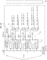
- FIG. 1A and 1B is structured around an Advanced Peripheral Bus (APB) and is intended to co-operate with a Fault Collection Unit interface (FCU Intf.) and a Self-Test Control Unit interface (STCU Intf.)
- APB Advanced Peripheral Bus
- FCU Intf. Fault Collection Unit interface
- STCU Intf. Self-Test Control Unit interface
- test stimuli for (at least) one circuit under test are pseudo-randomly generated using a certain number of LFSRs (LFSR_1_1, LFSR_1_2, ..., LFSR_M_NM) collectively designated 12.
- circuit under test can apply to multiple instances of different DUTs (designs under test) with different complexity and mutually (totally) independent (e.g., belonging to different sub-systems, design units etc. in a device).
- test stimuli may have associated therewith (in a manner known per se to those of skill in the art):
- test results for the circuits under test are collected and compressed in multiple input signature register blocks collectively designated 14.
- Each such block 14 comprises a Multiple Input Signature Register (MISR - COMPRESSOR_1, COMPRESSOR_2, ..., COMPRESSOR_N with an associated register (SIGNATURE_1_G, SIGNATURE_2_G, ..., SIGNATURE_N_G) configured to have stored therein a "golden” value.
- MISR Multiple Input Signature Register
- test results may include (in a manner known per se to those of skill in the art) respective sets of data such as OUT_TEST_DATA_1, OUT_TEST_DATA_2, ..., OUT_TEST_DATA_X1; OUT_TEST_DATA_X1+1, OUT_TEST_DATA_X1+2, OUT_TEST_DATA_X1+X2; OUT_TEST_DATA_X1+X2+ ... XN-1+1, OUT_TEST_DATA_X1+X2+ ... XN-1+2, ..., OUT_TEST_DATA_X1+X2+ ... XN-1+XN.
- the test campaign of each instantiated LFSR 12 can be configured runtime by associated control logic, LFSR_X_X_CNTRL (namely LFSR_1_1_CTRL, LFSR_1_2_CTRL, ..., LFSR_M_NM_CTRL, collectively designated 16 in Figure 1A ) having internal control registers, LBIST _X_X_CTRL_REG (namely LBIST_1_1_CTRL_REG, LBIST_1_2_CTRL, ..., LBIST_M_NM-CTRL, collectively designated 18 in Figure 1A and having associated timers T) which are written via software through the interface APB.
- LFSR_X_X_CNTRL namely LFSR_1_1_CTRL, LFSR_1_2_CTRL, ..., LFSR_M_NM_CTRL, collectively designated 16 in Figure 1A
- LBIST _X_X_CTRL_REG namely LBIST_1_1_
- each control logic module LFSR_X_X_CNTRL (namely LFSR_1_1_CTRL, LFSR_1_2_CTRL, ..., LFSR_M_NM_CTRL) in the set designated 16 drives all the output control signals for a certain LFSR 12 (LFSR_1_1, LFSR_1_2, ..., LFSR_M_NM).
- control signals driven by each bloc LFSR_X_X_CNTRL (16, namely LFSR_1_1_CTRL, LFSR_1_2_CTRL, ..., LFSR_M_NM_CTRL) include, in addition to EN e CLR, also TEST_MODE, SCAN_IN, etc.
- Figure 1A is thus exemplary of a circuit 10 comprising:
- an error signal ERR_1, ERR_2, ..., ERR_N may be triggered out on the FCU interface FCU Intf. at the end of the test campaign.
- Figure 1B is exemplary of the provision of:
- the signature control circuitry is configured to:
- Error signals ERR_1, ..., ERR_N may thus be produced in response to the signature comparison signals COMPRESSOR _1, COMPRESSOR _2, ..., COMPRESSOR_N produced from the test outcome signals OUT_TEST_DATA_1, ..., OUT_TEST_DATA_X1+X2+...+XN-1+XN received from the at least one circuit under test 200 failing to match with respective signature reference signals stored in the input signature registers SIGNATURE_1_G, SIGNATURE_2_G, ..., SIGNATURE_N_G.
- one or more embodiments are primarily concerned with (self-test) architecture as discussed rather than with the criteria adopted for selecting/programming the signature reference signals stored in the input signature registers SIGNATURE_1_G, SIGNATURE_2_G, ..., SIGNATURE_N_G and/or in the check for match or mismatch as performed in the signature control modules SIGN_1_CTRL, SIGN_2_CTRL, ..., SIGN_N_CTRL, collectively designated 20 in Figure 1B .
- test architecture as discussed herein is largely “transparent" to these criteria.
- an internal status register 22 can be provided for a finer error analysis, with a status bit for each test cluster.
- the end of an LFSR test campaign can be signaled by a pulse using an interrupt interface, one interrupt channel per instantiated LFSR.
- Each sub-block in the architecture of the circuit 10 as discussed herein and the associated (static) configuration parameters can be defined in such a way to adapt the architecture to a variety of possible test criteria and scenarios (for instance, in view of the concept underlying the test session, the development of the test campaign and/or the test clusters adopted for test purposes).
- the structure and the sub-blocks of the architecture of the circuit 10 as discussed herein facilitates defining a set of static configuration parameters which overcome various drawbacks of conventional solutions.
- Table I annexed to the description and paginated with it contains a possible list of configuration parameters which can be made available to a designer.
- these parameters may include:
- test stimuli (left-hand side of Figure 1A ) used to fill the test wrapper input scan-chains (as discussed in the following in connection with Figure 3 ) are pseudo-randomly generated using internal LFSRs such as 12 whose type, number and output parallelism is defined statically.
- Output parallelism is found to represent a useful approach for tuning the test time as this facilitates changing the time involved in filling the input scan-chains.
- the choice of LFSR type is related to the coverage targets and the CUT complexity.
- Controller modules (such as those collectively designated 18 in Figure 1A ) can be automatically generated and associated to each LFSR instance, in order to drive its control signals and the control signals of the associated external test wrappers/clusters (e.g., TEST_CAPTURE, SCAN_IN_EN, SCAN_OUT_EN, TEST_MODE, and so on).
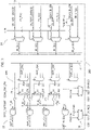
- Each controller module 16 can be programmed via SW by means of a dedicated control register (LBIST_1_1_CTRL_REG, LBIST_1_2_CTRL_REG, ..., LBIST_M_NM_CTRL _REG) out of the resisters collectively designated 18 and having the structure illustrated in Figure 2 for a generic register LBIST_x_x_CTRL_REG.
- LBIST_1_1_CTRL_REG LBIST_1_CTRL_REG
- LBIST_1_2_CTRL_REG LBIST_1_2_CTRL_REG
- LBIST_M_NM_CTRL _REG LBIST_M_NM_CTRL _REG
- N_TSESSIONS and N_TCYCLES register fields there is a number of N_TSESSIONS and N_TCYCLES register fields (the suffix is omitted for simplicity) equal to the number of associated test clusters, N_T_CLUSTER[i].
- Table II annexed to the description and paginated with it contains a detailed description of the fields in a register LBIST_x_x_CTRL_REG.
- the START bit is used to start via SW a test campaign which is made of a certain number of test sessions whose value can be programmed using the relative register field, N_TSESSIONS. Such value does not exceed the statically defined maximum value, N_TSESSIONS[i].
- N_TCYCLES For each test session is also possible to program a desired number of test cycles, N_TCYCLES, which facilitates tuning the test coverage.
- the start signal may be obtained from an end of counter (EOC) signal of an internal counter whose period can be programmed by SW.
- the N_CAPTURE _CYCLES register field is used to generate a configurable number of capture cycles, which is useful to increase the test coverage when the CUT contains sequential elements.
- the MULTI_CYCLE field if activated, can be used to insert an extra clock cycle in the test capture signal generation.
- control registers LBIST_1_1_CTRL_REG, LBIST_1_2_CTRL_REG, ..., LBIST_M_NM_CTRL_REG are configured to receive from the programming interface APB test programming information comprising:
- control registers LBIST_1_1_CTRL_REG, LBIST_1_2_CTRLREG, ..., LBIST_M_NM_CTRL_REG can be configured to receive from the test programming interface APB, in addition to test control information comprising capture mode information N_CAPTURE_CYCLES indicative of a number of capture cycles of output test signals for at least one circuit under test 200, also information (in the MULTI_CYCLE field) to insert extra cycles in the capture mode information N_CAPTURE_CYCLES.
- Figure 3 is illustrative of an exemplary test wrapper 200 configured to receive (to each test cluster) to collect the input test data coming from an associated LFSR (out of LFSR_1_1, LFSR_1_2, ..., LFSR_M_NM, collectively designated 12 in Figure 1A ) and transfer them to an input scan-chain and provide the generated test vectors to the CUTs.
- an LFSR out of LFSR_1_1, LFSR_1_2, ..., LFSR_M_NM, collectively designated 12 in Figure 1A
- the input test data IN_TEST DATA(0), IN_TEST_DATA(1), ... from architecture 10 as illustrated in Figures 1A and 1B can be applied to nodes in a logic circuitry LC (a HW safety mechanism or functional block, mostly combinational, for instance) which provides the circuits under test or CUTs.
- LC a HW safety mechanism or functional block, mostly combinational, for instance
- the input test data IN_TEST_DATA(0), IN_TEST_DATA(1), ... can be applied to the logic circuitry LC as an alternative to certain ones out "functional" signals IN_0(x), IN_1(x), IN_2(x), ..., IN-n-1(x) to homologous nodes IN_0(x), IN_1(x), IN_2(x), IN_n-1(x) in the logic circuitry LC via multiplexers collectively designated 24 acting under the control of a test mode signal T_M which is asserted to activate test mode operation.
- Signals OUT_0(x), OUT_1(x), OUT_2(x), ..., OUT_n-1(x) from the nodes of the logic circuitry LC are applied to multiplexers 26A in a set of flip-flops 26 connected in a cascaded scan chain arrangement controlled by SCAN_OUT_EN and TEST_CAPTURE signals (generated in a manner known per se to those of skill in the art).
- Reference 28 denotes collectively logic gates (AND gates, for instance) controlled by the test mode signal T_M (e.g. negated) to transfer the extract the "functional" outputs OUT_0(x), OUT_1(x), OUT_2(x), ..., OUT_m-1(x) from the logic circuitry LC.
- output test data OUT_TEST_DATA(0), OUT_TEST_DATA(1), ... are obtained from the test wrapper 200 (e.g. at multiplexers 30 coupled to the scan-chain 26).
- a scan chain such as illustrated at 26 comprises a set of flip-flops connected together to act as a sort of shift register when the design is in a Shift Test Mode (that is, with a SCAN_OUT_EN enable signal asserted).
- the first flip-flop of the scan chain is connected to a scan input and the last flip-flop in the scan chain is connected to a scan output.
- Scan chain operation can be regarded as involving three stages, namely scan in (this is the scan in shift mode phase where the FFs in the chain are loaded through scan in pins serially), capture (the design is kept in functional timing mode and test pattern response is captured) and scan out (this is the scanout shift mode phase where FFs in the chain are unloaded through scan out pins; scan-in phase can proceed concurrently).
- the CUT which is selected (in the network LC) is identified via signal encoding, one-hot encoding, the index of the test session, and the test mode signal T M in Figure 3 , which is driven by the LFSR controller.
- the same signal T M is used to route the CUT outputs to the wrapper output scan chain 26 and at the same time to gate them (via the gates 28) during a test session in order to avoid unwanted interferences with the rest of the SoC/IP arrangement.
- the number of FFs of the scan-chain of the i-th test wrapper can be changed automatically as a function of the values set for: LFSR_P[i] and N_TINPUTS_P[i] which is advantageous in terms of area cost
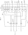
- funnels may be implemented with a structure as illustrated in Figure 4 .
- each X-OR gate in the circuitry 322 may receive two "homologous" inputs such as x1_0 and X2_0.
- a compression stage is provided comprising x-bit X-OR gates collectively designated 322.
- the value x denotes the compression ratio of the funnels 32 ( Figure 1B ), that is the ratio between the total number of input bits to a funnel (p1 + p2 + ... + pn) and the total number of output bits from the funnel.
- the connections between the AND gates 320 and the X-OR gates 322 results in grouping the output signals from the AND gates 320 in groups of x elements each starting from bit 0 of signal X1 and proceeding with bit 0 of signal X2, and so on up to bit 0 of signal Xn and then resuming with bit 1 of signal X1, then with bit 1 of signal X2, and so on up to bit 1 of signal Xn, proceeding in the same way for all the bits in the signals X1 to Xn.
- Figure 4 is thus exemplary of a possible, non mandatory, implementation of signature control circuitry configured to receive plural sets of test outcome signals from the circuit under test (200 in Figure 3 , with plural instances of the circuit 200 involved to have plural output sets) in response to the stimulus signals IN_TEST_DATA being applied to the at least one circuit under test with such compressor circuitry configured to produce from each one of the plural sets of test outcome signals from the at least one circuit under test 200 a respective signature comparison signal COMPRESSOR_1, COMPRESSOR _2, ..., COMPRESSOR_N for comparison with a respective reference signal in the set of signature control modules SIGN_1_CTRL, SIGN_2_CTRL, ..., SIGN_N_CTRL.
- COMPRESSOR_1, COMPRESSOR _2, ..., COMPRESSOR_N for comparison with a respective reference signal in the set of signature control modules SIGN_1_CTRL, SIGN_2_CTRL, ..., SIGN_N_CTRL.
- a possible mismatch between input and output data parallelism can be handled with or without adding extra data compression, in addition to the corresponding MISR processing, during a test campaign.
- Adding compression may somehow affect test coverage, with possible error masking due to aliasing, but at the same time decreases test time.
- the funnel/signature configuration register 32_1, 32_2, ..., 32_N in Figure 1B with one configuration register for funnel/signature instance.
- test output data generated during a test session or a test campaign con be compressed in multiple input signature registers (see 14 in Figure 1B ), whose parallelism is statically defined as the type and number of signatures which are instantiated.
- Each MISR block COMPRESSOR _1, COMPRESSOR_2, ..., COMPRESSOR_N has associated a respective register SIGNATURE_1_G, SIGNATURE_2_G, ..., SIGNATURE_N_G, which can be written via SW through the interface APB in order to store the expected/golden signature of a single test session or of an entire test campaign.
- the comparison between the computed "signature” values resulting from testing as stored COMPRESSOR_1, COMPRESSOR_2, ..., COMPRESSOR_N and the "golden” values stored in respective registers such as SIGNATURE_1_G, SIGNATURE_2_G, ..., SIGNATURE_N_G, can be configured via SW, using the funnel/signature configuration registers, at the end of a single test session or at the end of the entire test campaign of the associated LFSRs.
- the embodiments are primarily concerned with (self-test) architecture rather than with the criteria adopted for obtaining these test signatures and/or for performing match or mismatch checks in the signature control modules.
- test architecture as discussed herein is largely “transparent" to these criteria.
- the at least one second circuit 200 comprises:
- N_LFSR_TYPES integer Number of different LFSR types x pattern generation LFSR_TYPE[N_LFSR_TYPES] array of integers LFSR type information (length) N_LFSR[N_LFSR_TYPES] array of integers Number of instances x LFSR type N_LFSR_TOT integer Total number of LFSR instances sum(N LFSR) LFSR_P[N_LFSR_TOT] array of integers LFSR output parallelism for each LFSR instance N_T_CLUSTER[N_LFSR_TOT] array of integers Number of test clusters concurrently managed by each LFSR N_T_CLUSTER_TOT integer Total number of test clusters (CUTs) sum(N_T_CLUSTER) SIN_L[N_T_CLUSTER_TOT] array of integers Max length of the CUTs input
Landscapes
- Engineering & Computer Science (AREA)
- General Engineering & Computer Science (AREA)
- Physics & Mathematics (AREA)
- General Physics & Mathematics (AREA)
- Computer Hardware Design (AREA)
- Tests Of Electronic Circuits (AREA)
- Test And Diagnosis Of Digital Computers (AREA)
- Communication Control (AREA)
Abstract
Description
- The description relates to testing electronic circuits.
- One or more embodiments provide flexible architecture for online Logic Built-In Self-Test (LBIST) solutions. A configurable LBIST architecture for online/offline testing of (sub)systems may be exemplary of such architecture.
- One or more embodiments facilitate reducing the area overhead for desired coverage and test time targets in various scenarios such as intellectual property cores (IPs) or systems-on-chip (SoCs).
- Today, in sectors such as the automotive sector electronics is no longer used for implementing onboard comfort features only. Electronics is now extensively involved in implementing passive/active safety systems with the aim of preventing, or at least reducing, harm to driver and passenger(s): the related functions may involve functions such as, for instance, forward collision warning, blind spot monitoring, automatic emergency braking, airbag and ABS features and so on.
- This scenario underlies the adoption of specifications such as the ISO 26262 standard as applied to designing automotive electronics in order to provide a common basis to evaluate and document safety levels in electrical and electronics (E/E) systems.
- Adequately satisfying safety specifications such as ISO 26262, is facilitated by periodic online testing with the aim of detecting possible faults in the safety mechanisms implemented, latent point faults (LPFs) or single point faults (SPFs) in functional logic blocks.
- Despite the extensive activity in that area, products such as, for instance, SoCs and products for the automotive market will benefit from this availability of configurable on-line BIST (Built-In Self-Test) mechanisms able to test in an efficient way a variety of hardware (HW) safety mechanisms.
- An object of one or more embodiments is to contribute in providing improved solutions along the lines discussed in the foregoing.
- According to one or more embodiments, such an object can be achieved by means of a circuit having the features set forth in the claims that follow.
- A highly configurable LBIST architecture for online/offline testing of (sub)systems may be exemplary of such a circuit.
- One or more embodiments may relate to a corresponding device. A semiconductor device such as a SoC including self-test control architecture as illustrated herein (possibly in conjunction with associated scan-chain circuitry) may be exemplary of such a device.
- One or more embodiments may relate to a corresponding method.
- The claims are an integral part of the technical teaching on the embodiments as provided herein.
- One or more embodiments may provide one or more of the following advantages:
- an adequate trade-off in terms of area cost v. performance target (test coverage, test time) can be reached selecting (static) configuration parameters;
- integration in multiple simple/complex digital sub-systems for full/partial on-line Logic Built-In Self-Test (LBIST) testing of systems and sub-systems;
- a whole set of safety design/circuitry or just a programmable/configurable subset can be involved in testing;
- one or more test sessions can be triggered at runtime (e.g., via software) with reduced area overhead;
- the modules involved in a test session can be tested sequentially or in parallel: this level of configurability facilitates reaching an adequate trade-off in terms of area, test-time and coverage for various situations;
- as a side result, general "rules of thumb" for correct system sizing can be obtained.
- One or more embodiments will now be described, by way of example only, with reference to the annexed figures, wherein:
-
Figures 1A and1B jointly represent a block diagram of circuit architecture according to embodiments of the present description, -
Figure 2 is exemplary of fields which may be provided in registers included in architecture as illustrated inFigure 1 , -
Figure 3 is a block diagram of a test circuit configured to co-operate with architecture according to embodiments of the present description, and -
Figure 4 is a circuit diagram exemplary of parts of circuit architecture ofFigure 1B . - For the sake of convenience, two tables, designated Table I and Table II, are grouped together in two sheets annexed to the description and paginated with it.
- In the ensuing description, one or more specific details are illustrated, aimed at providing an in-depth understanding of examples of embodiments of this description. The embodiments may be obtained without one or more of the specific details, or with other methods, components, materials, etc. In other cases, known structures, materials, or operations are not illustrated or described in detail so that certain aspects of embodiments will not be obscured.
- Reference to "an embodiment" or "one embodiment" in the framework of the present description is intended to indicate that a particular configuration, structure, or characteristic described in relation to the embodiment is comprised in at least one embodiment. Hence, phrases such as "in an embodiment" or "in one embodiment" that may be present in one or more points of the present description do not necessarily refer to one and the same embodiment.
- Moreover, particular conformations, structures, or characteristics may be combined in any adequate way in one or more embodiments.
- The headings/references used herein are provided merely for convenience and hence do not define the extent of protection or the scope of the embodiments.
- Various acronyms are used for brevity throughout this description.
- While known to those of skill in the art, a number of these acronyms is reproduced below together with their meaning for immediate reference.

- SoC = System on Chip
- IP = Intellectual Property (core or block: a reusable unit of logic, cell, or integrated circuit layout design)

- CUT = Circuit Under Test

- MISR = Multiple Input Signature Register
- ECC = Error Correction Code
- FCU = Fault Collection Unit
- SPF = Single Point Fault
- LPF = Latent Point Fault
- EDPA = Enhanced Data Processing Architecture

- EOC = End of Counter
- One or more embodiments provide (circuit) architecture for periodic online/off-line LBIST operation.
- Static and dynamic configurability of the architecture makes is suited for use in testing various types of digital blocks (combinatorial or sequential).
- This also applies to complex blocks (e.g., sub-systems with many logic gates and memory elements).
- Moreover, one or more embodiments can handle concurrently (in an efficient way in terms of hardware involved) different types of circuit under test (CUT) and a different number of instances-per-type which may be present in a single IP or an entire SoC.
- It will be appreciated that, as used herein, the designation "circuit under test" (hence, the wording "at least one" circuit under test) can apply to multiple instances of different DUTs (designs under test) with different complexity and mutually (totally) independent (e.g., belonging to different sub-systems, design units etc. in a device).
- One or more embodiments involve a reduced area overhead. This facilitates applying a runtime LBIST feature also to small logic blocks such as ECC check/correction and generation ones. These are currently present in various automotive IPs and may be affected by latent faults.
- Nowadays, various CAD vendors propose proprietary solutions to automatically insert LBIST schemes in SoCs or IPs.
- Despite the flexibility which underlies designing and generating LBIST schemes, LBIST schemes generated and inserted automatically may not be able to provide concurrent tests using a single Linear-Feedback Shift Register (LFSR) and internal controller for different types of CUTs.
- Such limitations militate against a satisfactory trade-off between parameters such as area overhead, test coverage and time. This may be the case when CUTs are not particularly complex (e.g., logic blocks to generate and check different types of ECC schemes).
- A highly configurable LBIST scheme as discussed herein is able, thanks to its (static/dynamic) flexibility, to handle both complex and simple CUTs which may be present in an IP or in a SoC.
- One or more embodiments are based on hierarchical architecture comprising different types of sub-blocks, each dedicated to a particular functionality, whose number and internal parallelism can be configured (statically) during a configuration or design phase, via (static) RTL parameters. Also, internal connections and their parallelism can automatically change according to the values set for design parameters.
- Architecture as illustrated in
Figures 1A and1B is structured around an Advanced Peripheral Bus (APB) and is intended to co-operate with a Fault Collection Unit interface (FCU Intf.) and a Self-Test Control Unit interface (STCU Intf.) - As illustrated on the left-hand side of
Figure 1A , test stimuli for (at least) one circuit under test (200 - see alsoFigure 3 and the related discussion in the following) are pseudo-randomly generated using a certain number of LFSRs (LFSR_1_1, LFSR_1_2, ..., LFSR_M_NM) collectively designated 12. - As discussed previously, the designation "circuit under test" can apply to multiple instances of different DUTs (designs under test) with different complexity and mutually (totally) independent (e.g., belonging to different sub-systems, design units etc. in a device).
- As illustrated on the left-hand side of
Figure 1A , such test stimuli (IN_TEST_DATA signals) may have associated therewith (in a manner known per se to those of skill in the art): - a TEST MODE indicator;
- SCAN_IN_EN and SCAN_OUT_EN enable signals for scan_in and scan_out enable; and
- a test capture signal TEST_CAPTURE.
- As illustrated in
Figure 1B , test results for the circuits under test (200 - see alsoFigure 3 and the related discussion in the following) are collected and compressed in multiple input signature register blocks collectively designated 14. - Each
such block 14 comprises a Multiple Input Signature Register (MISR - COMPRESSOR_1, COMPRESSOR_2, ..., COMPRESSOR_N with an associated register (SIGNATURE_1_G, SIGNATURE_2_G, ..., SIGNATURE_N_G) configured to have stored therein a "golden" value. At the end of a test campaign or a single test session such a "golden" value is compared with the contents of the associated MISR: that is with the golden value stored in the register SIGNATURE_X compared with the value stored in the MISR COMPRESSOR_X. - As illustrated in
Figure 1B , such test results may include (in a manner known per se to those of skill in the art) respective sets of data such as OUT_TEST_DATA_1, OUT_TEST_DATA_2, ..., OUT_TEST_DATA_X1;OUT_TEST_DATA_X1+ 1, OUT_TEST_DATA_X1+2, OUT_TEST_DATA_X1+X2; OUT_TEST_DATA_X1+X2+ ... XN-1+1, OUT_TEST_DATA_X1+X2+ ... XN-1+2, ..., OUT_TEST_DATA_X1+X2+ ... XN-1+XN. - As illustrated in
Figure 1 , the test campaign of each instantiatedLFSR 12 can be configured runtime by associated control logic, LFSR_X_X_CNTRL (namely LFSR_1_1_CTRL, LFSR_1_2_CTRL, ..., LFSR_M_NM_CTRL, collectively designated 16 inFigure 1A ) having internal control registers, LBIST _X_X_CTRL_REG (namely LBIST_1_1_CTRL_REG, LBIST_1_2_CTRL, ..., LBIST_M_NM-CTRL, collectively designated 18 inFigure 1A and having associated timers T) which are written via software through the interface APB. - Based on the configuration written therein, each control logic module LFSR_X_X_CNTRL (namely LFSR_1_1_CTRL, LFSR_1_2_CTRL, ..., LFSR_M_NM_CTRL) in the set designated 16 drives all the output control signals for a certain LFSR 12 (LFSR_1_1, LFSR_1_2, ..., LFSR_M_NM).
- It is noted that the control signals driven by each bloc LFSR_X_X_CNTRL (16, namely LFSR_1_1_CTRL, LFSR_1_2_CTRL, ..., LFSR_M_NM_CTRL) include, in addition to EN e CLR, also TEST_MODE, SCAN_IN, etc.
- Briefly,
Figure 1A is thus exemplary of acircuit 10 comprising: - a set of
test stimulus generators 12, each generator in the set activatable to produce test stimulus signals IN_TEST_DATA for at least one circuit under test (200 inFigure 3 ) as a function of test stimulus information loaded in a test stimulus register LFSR_1_1, LFSR_1_2, ..., LFSR_M_NM in thegenerator 12, - a set of controllers collectively designated 16, namely LFSR_1_1_CTRL, LFSR_1_2_CTRL, ..., LFSR_M_NM_CTRL with each controller in the set configured to control loading of test stimulus information in the test stimulus register LFSR_1_1, LFSR_1_2, ..., LFSR_M_NM in a respective generator in the set of
test stimulus generators 12 as a function of test control information loaded in a respective control register LBIST_1_1_CTRL_REG, LBIST_1_2_CTRL_REG, ..., LBIST_M_NM_CTRL_REG in a set of control register designated collectively 18, - a programming interface APB configured to load test programming information such as START, MULTI_CYCLE, TIMER MODE, N_CAPTURE_CYCLES, N_TSESSIONS_x_x, N_TCYCLES_x_x as discussed in the following in the control registers 18, wherein the
test stimulus generators 12 are activatable as a function of test programming information such as START, MULTI_CYCLE, TIMER MODE, N_CAPTURE_CYCLES, N_TSESSIONS_x_x, N_TCYCLES_x_x loaded in the control registers 18 via the test programming interface APB. - In case of mismatches between the computed signature and the expected one as detected in signature control modules SIGN_1_CTRL, SIGN_2_CTRL, ..., SIGN_N_CTRL, collectively designated 20 in
Figure 1B , an error signal ERR_1, ERR_2, ..., ERR_N may be triggered out on the FCU interface FCU Intf. at the end of the test campaign. - Briefly,
Figure 1B is exemplary of the provision of: - a set of input signature registers SIGNATURE_1_G, SIGNATURE_2_G, ..., SIGNATURE_N_G, configured to store therein signature reference signals indicative of signature reference values received from the test programming interface (APB),
-
signature control circuitry set 20 of signature control modules SIGN_1_CTRL, SIGN_2_CTRL, ..., SIGN_N_CTRL coupled to respective ones of said input signature registers SIGNATURE_1_G, SIGNATURE_2_G, ..., SIGNATURE_N_G. - As illustrated herein, the signature control circuitry is configured to:
- receive from the at least one circuit under test (200 in
Figure 3 ) test outcome signals OUT_TEST_DATA_1, ..., OUT_TEST_DATA_X1+X2+...+XN-1+XN in response to the stimulus signals IN_TEST_DATA being applied thereto via thegenerators 12, - produce (at 32, for instance) from the test outcome signals OUT_TEST_DATA_1, ..., OUT_TEST_DATA_X1+X2+...+XN-1+XN) received from the circuit or
circuits 200 under test signature comparison signals COMPRESSOR _1, COMPRESSOR_2, ..., COMPRESSOR_N that are compared in the signature control modules SIGN_1_CTRL, SIGN_2_CTRL, ..., SIGN_N_CTRL with respective signature reference signals stored in the set of input signature registers SIGNATURE_1_G, SIGNATURE_2_G, ..., SIGNATURE_N_G. - Error signals ERR_1, ..., ERR_N may thus be produced in response to the signature comparison signals COMPRESSOR _1, COMPRESSOR _2, ..., COMPRESSOR_N produced from the test outcome signals OUT_TEST_DATA_1, ..., OUT_TEST_DATA_X1+X2+...+XN-1+XN received from the at least one circuit under
test 200 failing to match with respective signature reference signals stored in the input signature registers SIGNATURE_1_G, SIGNATURE_2_G, ..., SIGNATURE_N_G. - It is noted that one or more embodiments are primarily concerned with (self-test) architecture as discussed rather than with the criteria adopted for selecting/programming the signature reference signals stored in the input signature registers SIGNATURE_1_G, SIGNATURE_2_G, ..., SIGNATURE_N_G and/or in the check for match or mismatch as performed in the signature control modules SIGN_1_CTRL, SIGN_2_CTRL, ..., SIGN_N_CTRL, collectively designated 20 in
Figure 1B . - These criteria may be selected as a function of factors such as the nature and the type of the circuits under test, the intended application, the type of test(s) being performed an so on. These criteria can be selected in a wide variety of possible options known to those of skill in the art by otherwise noting that test architecture as discussed herein is largely "transparent" to these criteria.
- As illustrated, an
internal status register 22 can be provided for a finer error analysis, with a status bit for each test cluster. - The end of an LFSR test campaign can be signaled by a pulse using an interrupt interface, one interrupt channel per instantiated LFSR.
- Each sub-block in the architecture of the
circuit 10 as discussed herein and the associated (static) configuration parameters can be defined in such a way to adapt the architecture to a variety of possible test criteria and scenarios (for instance, in view of the concept underlying the test session, the development of the test campaign and/or the test clusters adopted for test purposes). - The structure and the sub-blocks of the architecture of the
circuit 10 as discussed herein facilitates defining a set of static configuration parameters which overcome various drawbacks of conventional solutions. - Table I annexed to the description and paginated with it contains a possible list of configuration parameters which can be made available to a designer.
- In the case of a 1D vector parameter the [] notation is used to express its dimension, while sum() is used to indicate the sum of the array elements.
- In detail, in an exemplary embodiment these parameters may include:
- an integer indicating the number of different LFSR types present inside the architecture, N_LFSR_TYPES;
- a vector of integers, one for each type, encoding the LFSR type information (e.g., 32 for a 32-bits LFSR, 16 for a 16-bits LFSR and so on), LFSR_TYPE[N_LFSR_TYPES];
- a vector of integers indicating the number of instances for each LFSR type, N_LFSR[N_LFSR_TYPES]. The total number of instances is so given by the internal derived parameter: N_LFSR_TOT = sum(N_LFSR). An internal parameter is a parameter whose value is automatically computed by the code and cannot be set by the user;
- a vector of integers, one for each LFSR instance, indicating its output parallelism, LFSR_P[N_LFSR_TOT]
- a vector of integers, one for each LFSR instance, indicating the number of test clusters handled in parallel by each LFSR, N_T_CLUSTER[N_LFSR_TOT]. As discussed herein, a test cluster is a group made of a certain number #N of CUTs serially tested using a common test session repeated #N times, usually the CUTs are of the same type and a dedicated test wrapper is inserted for each test cluster. While a test session is the set of the generated input test data, the total number of test clusters is given by the internal derived parameter: N_T_CLUSTER_TOT = sum(N_T_CLUSTER);
- a vector of integers, one for each test cluster, indicating the maximum length of the CUTs input scan-chains associated to that particular cluster, SIN_L[N_T_CLUSTER_TOT];
- a vector of integers, one for each test cluster, indicating the maximum length of the CUTs output scan-chains associated to that particular cluster, SOUT_L[N_T_CLUSTER_TOT];
- a vector of integers, one for each test cluster, indicating the maximum number of test sessions that can be programmed to be executed serially for that particular cluster, #N_TSESSIONS[N_T_CLUSTER_TOT];
- an integer indicating the number of different instantiated signature types inside the architecture, #N_MISR_TYPES;
- a vector of integers, one for each type, encoding the signature type information (e.g. 32 for a 32-bits MISR, 16 for a 16-bits MISR and so on), MISR_TYPE[N_MISR _TYPES];
- a vector of integers indicating the number of instances for each signature type, N_MISR[N_MISR_TYPES], the total number of instances is given by the internal derived parameter: N_MISR_TOT = sum(N_MISR) if <= N_T_CLUSTER_TOT; otherwise, an error is flagged;
- a vector of integers, one for each signature instance, indicating its input parallelism, MISR_P[N_MISR_TOT];
- a vector of integers, one for each input test data signal, indicating its parallelism, N_TINPUTS_P[N_T_CLUSTER_TOT]. The number of different input test data is equal to the total number of test clusters;
- a vector of integers, one for each signature, indicating the number of input test data signals/test clusters associated to that particular signature, N_MISR_TINPUTS[N_MISR_TOT]. Sum(N_MISR_TINPUTS) is equal to N_T_CLUSTER_TOT otherwise an error is flagged;
- an array of Boolean parameters, TIMER_MODE[N_LFSR_TOT], used to enable/disable the presence of the internal timer for each LFSR.
- A detailed description of exemplary sub-blocks included in architecture as illustrated in
Figures 1A and1B will now be provided together with a description of the possible impact of the associated configuration parameters. - The test stimuli (left-hand side of
Figure 1A ) used to fill the test wrapper input scan-chains (as discussed in the following in connection withFigure 3 ) are pseudo-randomly generated using internal LFSRs such as 12 whose type, number and output parallelism is defined statically. - Output parallelism is found to represent a useful approach for tuning the test time as this facilitates changing the time involved in filling the input scan-chains. The choice of LFSR type is related to the coverage targets and the CUT complexity.
- Controller modules (such as those collectively designated 18 in
Figure 1A ) can be automatically generated and associated to each LFSR instance, in order to drive its control signals and the control signals of the associated external test wrappers/clusters (e.g., TEST_CAPTURE, SCAN_IN_EN, SCAN_OUT_EN, TEST_MODE, and so on). - Each
controller module 16 can be programmed via SW by means of a dedicated control register (LBIST_1_1_CTRL_REG, LBIST_1_2_CTRL_REG, ..., LBIST_M_NM_CTRL _REG) out of the resisters collectively designated 18 and having the structure illustrated inFigure 2 for a generic register LBIST_x_x_CTRL_REG. - As illustrated in
Figure 2 , in addition to a START bit, MULTI_CYCLE and TIMER MODE fields and a number of N_CAPTURE_CYCLES, for the i-th controller there is a number of N_TSESSIONS and N_TCYCLES register fields (the suffix is omitted for simplicity) equal to the number of associated test clusters, N_T_CLUSTER[i]. - Table II annexed to the description and paginated with it contains a detailed description of the fields in a register LBIST_x_x_CTRL_REG.
- The START bit is used to start via SW a test campaign which is made of a certain number of test sessions whose value can be programmed using the relative register field, N_TSESSIONS. Such value does not exceed the statically defined maximum value, N_TSESSIONS[i].
- For each test session is also possible to program a desired number of test cycles, N_TCYCLES, which facilitates tuning the test coverage.
- A timer mode if (and only if) TIMER_MODE[i] is active, is also made available to trigger test campaigns at regular time intervals without SW intervention. In that case, the start signal may be obtained from an end of counter (EOC) signal of an internal counter whose period can be programmed by SW.
- The N_CAPTURE _CYCLES register field is used to generate a configurable number of capture cycles, which is useful to increase the test coverage when the CUT contains sequential elements. The MULTI_CYCLE field, if activated, can be used to insert an extra clock cycle in the test capture signal generation.
- In a particularly advantageous manner, the control registers LBIST_1_1_CTRL_REG, LBIST_1_2_CTRL_REG, ..., LBIST_M_NM_CTRL_REG are configured to receive from the programming interface APB test programming information comprising:
- a number of test sessions N_TSESSIONS_x_x for which a test stimulus generator is activated to produce test stimulus signals IN_TEST_DATA for at least one circuit under
test 200, and/or - a number of test cycles N_TCYCLES for which a
test stimulus generator 12 is activated in a test session for at least one circuit undertest 200, and/or - timed test mode activation information TIMER_MODE to activate a
test stimulus generator 12 at programmed times, and/or - capture mode information N_CAPTURE_CYCLES indicative of a number of capture cycles of output test signals for at least one circuit under
test 200. - In this last-cited case, the control registers LBIST_1_1_CTRL_REG, LBIST_1_2_CTRLREG, ..., LBIST_M_NM_CTRL_REG can be configured to receive from the test programming interface APB, in addition to test control information comprising capture mode information N_CAPTURE_CYCLES indicative of a number of capture cycles of output test signals for at least one circuit under
test 200, also information (in the MULTI_CYCLE field) to insert extra cycles in the capture mode information N_CAPTURE_CYCLES. -
Figure 3 is illustrative of anexemplary test wrapper 200 configured to receive (to each test cluster) to collect the input test data coming from an associated LFSR (out of LFSR_1_1, LFSR_1_2, ..., LFSR_M_NM, collectively designated 12 inFigure 1A ) and transfer them to an input scan-chain and provide the generated test vectors to the CUTs. - As detailed in
Figure 3 (and otherwise known in scan chain operation), the input test data IN_TEST DATA(0), IN_TEST_DATA(1), ... fromarchitecture 10 as illustrated inFigures 1A and1B can be applied to nodes in a logic circuitry LC (a HW safety mechanism or functional block, mostly combinational, for instance) which provides the circuits under test or CUTs. - The input test data IN_TEST_DATA(0), IN_TEST_DATA(1), ... can be applied to the logic circuitry LC as an alternative to certain ones out "functional" signals IN_0(x), IN_1(x), IN_2(x), ..., IN-n-1(x) to homologous nodes IN_0(x), IN_1(x), IN_2(x), IN_n-1(x) in the logic circuitry LC via multiplexers collectively designated 24 acting under the control of a test mode signal T_M which is asserted to activate test mode operation.
- Signals OUT_0(x), OUT_1(x), OUT_2(x), ..., OUT_n-1(x) from the nodes of the logic circuitry LC are applied to multiplexers 26A in a set of flip-
flops 26 connected in a cascaded scan chain arrangement controlled by SCAN_OUT_EN and TEST_CAPTURE signals (generated in a manner known per se to those of skill in the art). -
Reference 28 denotes collectively logic gates (AND gates, for instance) controlled by the test mode signal T_M (e.g. negated) to transfer the extract the "functional" outputs OUT_0(x), OUT_1(x), OUT_2(x), ..., OUT_m-1(x) from the logic circuitry LC. - As exemplified in
Figure 3 , output test data OUT_TEST_DATA(0), OUT_TEST_DATA(1), ... are obtained from the test wrapper 200 (e.g. atmultiplexers 30 coupled to the scan-chain 26). - Briefly, a scan chain such as illustrated at 26 comprises a set of flip-flops connected together to act as a sort of shift register when the design is in a Shift Test Mode (that is, with a SCAN_OUT_EN enable signal asserted).
- Referring for simplicity to an input and output parallelism equal to 1, the first flip-flop of the scan chain is connected to a scan input and the last flip-flop in the scan chain is connected to a scan output.
- Scan chain operation can be regarded as involving three stages, namely scan in (this is the scan in shift mode phase where the FFs in the chain are loaded through scan in pins serially), capture (the design is kept in functional timing mode and test pattern response is captured) and scan out (this is the scanout shift mode phase where FFs in the chain are unloaded through scan out pins; scan-in phase can proceed concurrently).
- Structure and operation of a scan chain as discussed previously, including a SCA_IN_EN enable signals and a signal derive from one of the flip-flops (e.g., FFn-2) being applied to the
multiplexers 24, is otherwise conventional in the art. - Reference may be had in that respect, merely by way of example, to S. Sharma: "Scan Chains: PnR Outlook" (see design-reuse.com). This makes it unnecessary to provide a more detailed description herein.
- For the purposes herein it will be appreciated that the CUT which is selected (in the network LC) is identified via signal encoding, one-hot encoding, the index of the test session, and the test mode signal T M in
Figure 3 , which is driven by the LFSR controller. - The same signal T M is used to route the CUT outputs to the wrapper
output scan chain 26 and at the same time to gate them (via the gates 28) during a test session in order to avoid unwanted interferences with the rest of the SoC/IP arrangement. - The number of FFs of the scan-chain of the i-th test wrapper can be changed automatically as a function of the values set for: LFSR_P[i] and N_TINPUTS_P[i] which is advantageous in terms of area cost
- As illustrated on the right-hand side of
Figure 1B , so-called internal "funnels", FUNNEL_1, FUNNEL_2, ..., FUNNEL_N collectively designated 32 can be used to associate a respective set of data such as OUT_TEST_DATA_1, OUT_TEST_DATA_2, ..., OUT_TEST_DATA_X1;OUT_TEST_DATA_X1+ 1, OUT_TEST_DATA_X1+2, OUT_TEST_DATA_X1+X2; OUT_TEST_DATA_X1+X2+ ... XN-1+1, OUT_TEST_DATA_X1+X2+ ... XN-1+2, ..., OUT_TEST_DATA_X1+X2+ ... XN-1+XN. - to a single signature register SIGNATURE_1_G, SIGNATURE_2_G, ..., SIGNATURE_N_G (see 14 in
Figure 1B ) with its own parallelism. - These funnels may be implemented with a structure as illustrated in
Figure 4 . - In the arrangement exemplified
Figure 4 , the data from one the sets above, briefly indicated as - X1_0, X1_1, X1_2, ..., X1_p1-1;
- X2_0, X2_1, ..., X2_p2-1;
- Xn_0,..., Xn_pn-1
- As illustrated in
Figure 4 each X-OR gate in thecircuitry 322 may receive two "homologous" inputs such as x1_0 and X2_0. - After the gating stage (that is, the AND gates collectively designated 320), a compression stage is provided inclusing x-bit X-OR gates collectively designated 322. There, the value x denotes the compression ratio of the funnels 32 (
Figure 1B ), that is the ratio between the total number of input bits to a funnel (p1 + p2 + ... + pn) and the total number of output bits from the funnel. - This last value is equal to the input parallelism of the associated signature and is statically defined by the MISR_P [N_MISR_TOT] parameter. In
Figure 4 , by way of non-limiting example, x = 2: in fact eachX-OR gate 322 is shown to have two inputs. - As an implementation specification, the ratio x is an integer: in case x = 3, for instance,
X-OR gates 322 with three inputs are used. - As represented in
Figure 4 (schematically, in order to avoid an unduly complicated representation) the connections between the ANDgates 320 and theX-OR gates 322 results in grouping the output signals from the ANDgates 320 in groups of x elements each starting frombit 0 of signal X1 and proceeding withbit 0 of signal X2, and so on up tobit 0 of signal Xn and then resuming withbit 1 of signal X1, then withbit 1 of signal X2, and so on up tobit 1 of signal Xn, proceeding in the same way for all the bits in the signals X1 to Xn. - When all the bits of a signal are connected, this signal is excluded from the process and a jump is made to the bit of the first subsequent signal still to be managed. In that way signals with different amplitudes can be grouped together.
-
Figure 4 is thus exemplary of a possible, non mandatory, implementation of signature control circuitry configured to receive plural sets of test outcome signals from the circuit under test (200 inFigure 3 , with plural instances of thecircuit 200 involved to have plural output sets) in response to the stimulus signals IN_TEST_DATA being applied to the at least one circuit under test with such compressor circuitry configured to produce from each one of the plural sets of test outcome signals from the at least one circuit under test 200 a respective signature comparison signal COMPRESSOR_1, COMPRESSOR _2, ..., COMPRESSOR_N for comparison with a respective reference signal in the set of signature control modules SIGN_1_CTRL, SIGN_2_CTRL, ..., SIGN_N_CTRL. - A possible mismatch between input and output data parallelism can be handled with or without adding extra data compression, in addition to the corresponding MISR processing, during a test campaign.
- Adding compression may somehow affect test coverage, with possible error masking due to aliasing, but at the same time decreases test time.
- Which one of the funnel inputs is active is given by a dedicated configuration register, the funnel/signature configuration register 32_1, 32_2, ..., 32_N in
Figure 1B , with one configuration register for funnel/signature instance. - The test output data generated during a test session or a test campaign con be compressed in multiple input signature registers (see 14 in
Figure 1B ), whose parallelism is statically defined as the type and number of signatures which are instantiated. - Each MISR block COMPRESSOR _1, COMPRESSOR_2, ..., COMPRESSOR_N has associated a respective register SIGNATURE_1_G, SIGNATURE_2_G, ..., SIGNATURE_N_G, which can be written via SW through the interface APB in order to store the expected/golden signature of a single test session or of an entire test campaign.
- The comparison between the computed "signature" values resulting from testing as stored COMPRESSOR_1, COMPRESSOR_2, ..., COMPRESSOR_N and the "golden" values stored in respective registers such as SIGNATURE_1_G, SIGNATURE_2_G, ..., SIGNATURE_N_G, can be configured via SW, using the funnel/signature configuration registers, at the end of a single test session or at the end of the entire test campaign of the associated LFSRs.
- It is once more noted that the embodiments are primarily concerned with (self-test) architecture rather than with the criteria adopted for obtaining these test signatures and/or for performing match or mismatch checks in the signature control modules.
- These criteria may be selected as a function of factors such as the nature and the type of the circuits under test, the intended application, the type of test(s) being performed and so on. These criteria can be selected in a wide variety of possible options known to those of skill in the art by otherwise noting that test architecture as discussed herein is largely "transparent" to these criteria.
- Such an architecture is thus applicable to a wide variety of devices comprising:
- a
first circuit 10 as exemplified inFigure 1A andFigure 1B , and - at least one
second circuit 200 as exemplified inFigure 3 and configured to be brought to a test mode (signal T_M) wherein during the test mode the at least one second circuit is coupled:- to the set of
test stimulus generators 12 in thefirst circuit 10 to receive therefrom the test stimulus signals (for instance IN_TEST_DATA and signals associated thereto, as discussed previously), and - to the
signature control circuitry
- to the set of
- As illustrated in
Figure 3 , the at least onesecond circuit 200 comprises: - logic circuitry LC candidate for testing, and
- scan-
chain circuitry - apply to the logic circuitry LC, during the test mode, test input data IN_0(x), IN_1 (x), ..., IN_n-1(x) as a function of the test stimulus signals from the
test stimulus generators 12 in thefirst circuit 10, and - recover from the logic circuitry LC during the test mode test output signals OUT_0(x), OUT_1 (x), ..., OUT_M-1(x) and apply the test output signals as test outcome signals OUT_TEST_DATA_1, ..., OUT_TEST_DATA_X1+X2+...+XN-1+XN to the
signature control circuitry first circuit 10.
- apply to the logic circuitry LC, during the test mode, test input data IN_0(x), IN_1 (x), ..., IN_n-1(x) as a function of the test stimulus signals from the
- Architecture as discussed herein and the associated set of RTL configuration parameters is advantageous in testing various types and configurations of CUTs both at IP and SoC level overcoming certain limitations of conventional solutions. This applies particularly when many different types and instances of simple CUTs are concurrently handled by testing architecture without duplicating the LBIST controllers.
- For instance, the solution discussed here was successfully used in connection with an EDPA safety mechanisms as disclosed in
Italian patent applications Nos. 102020000009358 102020000029759 - Without prejudice to the underlying principles, the details and embodiments may vary, even significantly, with respect to what has been described by way of example only without departing from the extent of protection.
- The extent of protection is determined by the annexed claims.
TABLE I - Configuration parameters PARAMETER TYPE DESCRIPTION NOTE N_LFSR_TYPES integer Number of different LFSR types x pattern generation LFSR_TYPE[N_LFSR_TYPES] array of integers LFSR type information (length) N_LFSR[N_LFSR_TYPES] array of integers Number of instances x LFSR type N_LFSR_TOT integer Total number of LFSR instances sum(N LFSR) LFSR_P[N_LFSR_TOT] array of integers LFSR output parallelism for each LFSR instance N_T_CLUSTER[N_LFSR_TOT] array of integers Number of test clusters concurrently managed by each LFSR N_T_CLUSTER_TOT integer Total number of test clusters (CUTs) sum(N_T_CLU STER) SIN_L[N_T_CLUSTER_TOT] array of integers Max length of the CUTs input scan chains for each test cluster SOUT_L[N_T_CLUSTER_TOT] array of integers Max length of the CUTs output scan chains for each test cluster #N_TSESSIONS[N_T_CLUSTER_T OT] array of integers Max number of test sessions programmable for each test cluster #N_MISR_TYPES integer Number of different MISR types x signature compression MISR_TYPE[N_MISR_TYPES] array of integers MISR type information (length) N_MISR[N_MISR_TYPES] array of integers Number of instances x MISR type N_MISR_TOT integer Total number of MISR instances N MISR TOT <= N T CLUSTER TOT sum(N_MISR) MISR_P[N_MISR_TOT] array of integers MISR input parallelism for each MISR instance TINPUTS_P[N_T_CLUSTER_TOT] . array of integers Number of input test data for each test cluster N_MISR_TINPUTS [N_MISR_TOT] array of Number of input test data for each integers MISR Sum(N_MISR_TINPUTS) = N T CLUSTER TOT TIMER_MODE[N_LFSR_TOT] array of integers Enable/disable an internal timer x LFSR optional TABLE II - Fields in a register LBIST x x CTRL REG. Field Type Description START Boolean To start the test campaign of a certain number of test sessions MULTI_CYCLE Boolean 2 clock periods in the capture cycle to reduce the actual clock frequency (in case of critical timing paths) TIMER MODE Boolean Timer mode to trigger the test campaign on regular time interval N_CAPTURE_CYCLES Integer Number of capture cycles (for almost full-scan design) N_TSESSIONS_x_x array of integers Number of test sessions <= N_TSESSIONS[i] for each test cluster N_TCYCLES_x_X array of integers Number of test cycles <= N_TSESSIONS[i] for each test session
Claims (9)
- A circuit (10), comprising:a set of test stimulus generators (12), each generator in the set activatable to produce test stimulus signals (IN_TEST_DATA) for at least one circuit under test (200) as a function of test stimulus information loaded in a test stimulus register (LFSR_1_1, LFSR_1_2, ..., LFSR_M_NM) in the generator (12),a set of controllers (16; LFSR_1_1_CTRL, LFSR_1_2_CTRL, ..., LFSR_M_NM_CTRL), each controller in the set configured to control loading of test stimulus information in the test stimulus register (LFSR_1_1, LFSR_1_2, ..., LFSR_M_NM) in a respective generator in the set of test stimulus generators (12) as a function of test control information loaded in a respective control register (LBIST_1_1_CTRL_REG, LBIST_1_2_CTRL_REG, ..., LBIST_M_NM_CTRL_REG) in a set of control registers (18),a programming interface (APB) configured to load test programming information (START, MULTI_CYCLE, TIMER MODE, N_CAPTURE_CYCLES, N_TSESSIONS_x_x, N_TCYCLES_x_x) in the control registers in said set of control registers (18), wherein the test stimulus generators in the set of test stimulus generators (12) are activatable as a function of test programming information (START, MULTI_CYCLE, TIMER MODE, N_CAPTURE_CYCLES, N_TSESSIONS_x_x, N_TCYCLES_x_x) loaded in the control registers in said set of control registers (18) via said test programming interface (APB);a set of input signature registers (SIGNATURE_1_G, SIGNATURE_2_G, ..., SIGNATURE_N_G), configured to store therein signature reference signals indicative of signature reference values received from said test programming interface (APB),signature control circuitry (14, 20, 22, 32) comprising a set (20) of signature control modules (SIGN_1_CTRL, SIGN_2_CTRL, ..., SIGN_N_CTRL) coupled to respective ones of said input signature registers (SIGNATURE_1_G, SIGNATURE_2_G, ..., SIGNATURE_N_G), the signature control circuitry configured to:receive from said at least one circuit under test (200) test outcome signals (OUT_TEST_DATA_1, ..., OUT_TEST_DATA_X1+X2+...+XN-1+XN) in response to said stimulus signals (IN_TEST_DATA) being applied thereto,produce (32) from the test outcome signals (OUT_TEST_DATA_1, ..., OUT_TEST_DATAX1+X2+...+XN-1+XN) received from said at least one circuit under test (200) signature comparison signals (COMPRESSOR_1, COMPRESSOR_2, ..., COMPRESSOR_N),compare (20) in said set (20) of signature control modules (SIGN_1_CTRL, SIGN_2_CTRL, ..., SIGN_N_CTRL) the signature comparison signals (COMPRESSOR_1, COMPRESSOR_2, ..., COMPRESSOR_N) produced (32) from the test outcome signals (OUT_TEST_DATA_1, ..., OUT_TEST_DATA_X1+X2+...+XN-1+XN) received from said at least one circuit under test (200) with respective signature reference signals in said set of input signature registers (SIGNATURE_1_G, SIGNATURE_2_G, ..., SIGNATURE_N_G), andproduce (20) error signals (ERR_1, ..., ERR_N) in response to the signature comparison signals (COMPRESSOR _1, COMPRESSOR _2, ..., COMPRESSOR_N) produced (32) from the test outcome signals (OUT_TEST_DATA_1, ..., OUT_TEST_DATA_X1+X2+...+XN-1+XN) received from said at least one circuit under test (200) failing to match with respective signature reference signals in said set of input signature registers (SIGNATURE_1_G, SIGNATURE_2_G, ..., SIGNATURE_N_G).
- The circuit (10) of claim 1, wherein the control registers (LBIST_1_1_CTRL_REG, LBIST_1_2_CTRL_REG, ..., LBIST_M_NM_CTRL_REG) in said set of control register (18) are configured (START, MULTI_CYCLE, TIMER MODE, N_CAPTURE_CYCLES, N_TSESSIONS_x_x, N_TCYCLES_x_x) to receive from said interface (APB) test programming information comprising:a number of test sessions (N_TSESSIONS_x_x) for which a test stimulus generator in the set of test stimulus generators (12) is activated to produce test stimulus signals (IN_TEST_DATA) for at least one circuit under test (200), and/ora number of test cycles (N_TCYCLES) for which a test stimulus generator in the set of test stimulus generators (12) is activated in a test session for at least one circuit under test (200), and/ortimed test mode activation information (TIMER MODE) to activate a test stimulus generator in the set of test stimulus generators (12) at programmed times, and/orcapture mode information (N_CAPTURE_CYCLES) indicative of a number of capture cycles of output test signals for at least one circuit under test (200).
- The circuit (10) of claim 2, wherein the control registers (LBIST_1_1_CTRL_REG, LBIST_1_2_CTRL_REG, ..., LBIST_M_NM_CTRL_REG) in said set of control register (18) are configured to receive from said test programming interface (APB) test control information comprising capture mode information (N_CAPTURE_CYCLES) indicative of a number of capture cycles of output test signals for at least one circuit under test (200) as well as information (MULTI_CYCLE) to insert extra cycles in said capture mode information (N_CAPTURE_CYCLES).
- The circuit (10) of any of the previous claims, wherein the generators in said set of test stimulus generators (12) comprise linear-feedback shift register as said test stimulus register (LFSR_1_1, LFSR_1_2, ..., LFSR_M_NM) in the generator (12).
- The circuit (10) of any of the previous claims, wherein the generators in said set of test stimulus generators (12) are configured to produce test stimulus signals (IN_TEST_DATA) for at least one circuit under test (200) having coupled therewith signals selected out of:a test mode indicator signal (TEST MODE);scan_in and scan_out enable signals (SCAN_IN_EN, SCAN_OUT_EN); and/ora test capture signal (TEST_CAPTURE).
- The circuit (10) of any of the previous claims, wherein the signature control circuitry (14, 20, 22, 32) comprises compressor circuitry (32; FUNNEL _1, ..., FUNNEL_N; COMPRESSOR _1, ..., COMPRESSOR_N) configured to receive plural sets of test outcome signals from said at least one circuit under test (200) in response to said stimulus signals (IN_TEST_DATA) being applied thereto, the compressor circuitry (32; FUNNEL_1, ..., FUNNEL_N; COMPRESSOR _1, ..., COMPRESSOR_N) configured to produce from each one of said plural sets of test outcome signals from said at least one circuit under test (200) a respective signature comparison signal (COMPRESSOR_1, COMPRESSOR_2, ..., COMPRESSOR_N) for comparison with a respective reference signal in said set (20) of signature control modules (SIGN_1_CTRL, SIGN_2_CTRL, ..., SIGN_N_CTRL) .
- A device (10, 200), comprising:a first circuit (10), the first circuit according to any of the previous claims, andat least one second circuit (200) configured to be brought to a test mode (T_M) wherein during said test mode (T_M) the at least one second circuit (200) is coupled:to said set of test stimulus generators (12) in the first circuit (10) to receive therefrom said test stimulus signals (IN_TEST_DATA), andto said signature control circuitry (14, 20, 22, 32) to provide thereto said test outcome signals (OUT_TEST_DATA_1, ..., OUT_TEST_DATA_X1+X2+...+XN-1+XN) in response to said stimulus signals (IN_TEST_DATA) being applied thereto.
- The device (10, 200) of claim 7, wherein the at least one second circuit (200) comprises:logic circuitry (LC) candidate for testing, andscan-chain circuitry (24, 26) configured to:apply to said logic circuitry (LC) during said test mode (T_M) test input data (IN_0(x), IN_1 (x), ..., IN_n-1(x) as a function of said test stimulus signals (IN_TEST_DATA) from the set of test stimulus generators (12) in the first circuit (10), andrecover from said logic circuitry (LC) during said test mode (T_M) test output signals (OUT_0(x), OUT_1 (x), ..., OUT_M-1(x)) and apply said test output signals (OUT_0(x), OUT-1 (x), ..., OUT_m-1 (x)) as test outcome signals (OUT_TEST_DATA_1, ..., OUT_TEST_DATA_X1+X2+...+XN-1+XN) to said signature control circuitry (14, 20, 22, 32) in the first circuit (10).
- A method, comprising:applying (200) to at least one circuit under test (200) test stimulus signals (IN_TEST_DATA) produced in a set of test stimulus generators (12) as a function of test stimulus information loaded in test stimulus registers (LFSR_1_1, LFSR_1_2, ..., LFSR_M_NM) in said stimulus generators (12),controlling (16; LFSR_1_1_CTRL, LFSR_1_2_CTRL, ..., LFSR_M_NM_CTRL) loading of test stimulus information in the test stimulus registers (LFSR_1_1, LFSR_1_2, ..., LFSR M NM) of said test stimulus generators (12) as a function of test programming information (START, MULTI_CYCLE, TIMER MODE, N_CAPTURE_CYCLES, N_TSESSIONS_x_x, N_TCYCLES_x_x) loaded (APB) in a respective control register (LBIST_1_1_CTRL_REG, LBIST_1_2_CTRL_REG, ..., LBIST_M_NM_CTRL_REG) in a set of control registers (18), wherein said test stimulus generators (12) are activated as a function of said test programming information (START, MULTI_CYCLE, TIMER MODE, N_CAPTURE_CYCLES, N_TSESSIONS_x_x, N_TCYCLES_x_x) loaded in said control registers (18),receiving test outcome signals (OUT_TEST_DATA_1,..., OUT_TEST_DATA_X1+X2+...+XN-1+XN) from said at least one circuit under test (200) in response to said stimulus signals (IN_TEST_DATA) being applied thereto,producing (32) signature comparison signals (COMPRESSOR_1, COMPRESSOR_2, ..., COMPRESSOR_N) from the test outcome signals (OUT_TEST_DATA_1, ..., OUT_TEST_DATA_X1+X2+...+XN-1+XN) received from said at least one circuit under test (200),comparing the signature comparison signals (COMPRESSOR _1, COMPRESSOR _2, ..., COMPRESSOR_N) produced (32) from the test outcome signals (OUT_TEST_DATA_1, ..., OUT_TEST_DATA_X1+X2+...+XN-1+XN) received from said at least one circuit under test (200) with respective programmable (APB) signature reference signals stored in a set of input signature registers (SIGNATURE_1_G, SIGNATURE_2_G, ..., SIGNATURE_N_G), andproducing (20) error signals (ERR_1, ..., ERR_N) in response to the signature comparison signals (COMPRESSOR _1, COMPRESSOR _2, ..., COMPRESSOR_N) produced (32) from the test outcome signals (OUT_TEST_DATA_1, ..., OUT_TEST_DATA_X1+X2+...+XN-1+XN) received from said at least one circuit under test (200) failing to match with said respective reference signals stored in a set of input signature registers (SIGNATURE_1_G, SIGNATURE_2_G, ..., SIGNATURE_N_G).
Applications Claiming Priority (1)
| Application Number | Priority Date | Filing Date | Title |
|---|---|---|---|
| IT102021000007856A IT202100007856A1 (en) | 2021-03-30 | 2021-03-30 | TEST ARCHITECTURE FOR ELECTRONIC CIRCUITS, CORRESPONDING DEVICE AND PROCEDURE |
Publications (1)
| Publication Number | Publication Date |
|---|---|
| EP4067918A1 true EP4067918A1 (en) | 2022-10-05 |
Family
ID=76270006
Family Applications (1)
| Application Number | Title | Priority Date | Filing Date |
|---|---|---|---|
| EP22160090.1A Withdrawn EP4067918A1 (en) | 2021-03-30 | 2022-03-03 | Test architecture for electronic circuits, corresponding device and method |
Country Status (3)
| Country | Link |
|---|---|
| US (1) | US11940492B2 (en) |
| EP (1) | EP4067918A1 (en) |
| IT (1) | IT202100007856A1 (en) |
Families Citing this family (2)
| Publication number | Priority date | Publication date | Assignee | Title |
|---|---|---|---|---|
| IT202100007856A1 (en) * | 2021-03-30 | 2022-09-30 | St Microelectronics Srl | TEST ARCHITECTURE FOR ELECTRONIC CIRCUITS, CORRESPONDING DEVICE AND PROCEDURE |
| US12072379B2 (en) * | 2022-03-14 | 2024-08-27 | Duke University | Dynamic scan obfuscation for integrated circuit protections |
Citations (3)
| Publication number | Priority date | Publication date | Assignee | Title |
|---|---|---|---|---|
| US20070011537A1 (en) * | 2005-06-22 | 2007-01-11 | Toshiba America Electronic Components | Systems and methods for self-diagnosing LBIST |
| US20140053034A1 (en) * | 2012-08-15 | 2014-02-20 | International Business Machines Corporation | On-chip detection of types of operations tested by an lbist |
| US20180067164A1 (en) * | 2016-09-06 | 2018-03-08 | Texas Instruments Incorporated | Multiple input signature register analysis for digital circuitry |
Family Cites Families (24)
| Publication number | Priority date | Publication date | Assignee | Title |
|---|---|---|---|---|
| US5991909A (en) * | 1996-10-15 | 1999-11-23 | Mentor Graphics Corporation | Parallel decompressor and related methods and apparatuses |
| US6148425A (en) * | 1998-02-12 | 2000-11-14 | Lucent Technologies Inc. | Bist architecture for detecting path-delay faults in a sequential circuit |
| US6966021B2 (en) * | 1998-06-16 | 2005-11-15 | Janusz Rajski | Method and apparatus for at-speed testing of digital circuits |
| US6694466B1 (en) * | 1999-10-27 | 2004-02-17 | Agere Systems Inc. | Method and system for improving the test quality for scan-based BIST using a general test application scheme |
| US6715105B1 (en) * | 2000-11-14 | 2004-03-30 | Agilent Technologies, Inc. | Method for reducing stored patterns for IC test by embedding built-in-self-test circuitry for chip logic into a scan test access port |
| US6789220B1 (en) * | 2001-05-03 | 2004-09-07 | Xilinx, Inc. | Method and apparatus for vector processing |
| US6950974B1 (en) * | 2001-09-07 | 2005-09-27 | Synopsys Inc. | Efficient compression and application of deterministic patterns in a logic BIST architecture |
| JP2003121499A (en) * | 2001-10-09 | 2003-04-23 | Hitachi Ltd | Semiconductor integrated circuit with built-in test function, storage medium for storing electronic design data comprising test code generation program, test method for semiconductor integrated circuit, test code generation automatic method, and program therefor |
| US7155648B2 (en) * | 2003-09-19 | 2006-12-26 | Intel Corporation | Linear feedback shift register reseeding |
| US7055077B2 (en) * | 2003-12-23 | 2006-05-30 | Kabushiki Kaisha Toshiba | Systems and methods for circuit testing |
| US7627798B2 (en) * | 2004-10-08 | 2009-12-01 | Kabushiki Kaisha Toshiba | Systems and methods for circuit testing using LBIST |
| US7941718B2 (en) * | 2006-03-07 | 2011-05-10 | Freescale Semiconductor, Inc. | Electronic device testing system |
| US7472324B2 (en) * | 2006-08-02 | 2008-12-30 | International Business Machines Corporation | Logic built-in self-test channel skipping during functional scan operations |
| US7661050B2 (en) * | 2007-05-04 | 2010-02-09 | International Business Machines Corporation | Method and system for formal verification of partial good self test fencing structures |
| US7908532B2 (en) * | 2008-02-16 | 2011-03-15 | International Business Machines Corporation | Automated system and processing for expedient diagnosis of broken shift registers latch chains |
| US8286042B2 (en) * | 2009-02-20 | 2012-10-09 | Texas Instruments Incorporated | On-chip seed generation using boolean functions for LFSR re-seeding based logic BIST techniques for low cost field testability |
| US8843797B2 (en) * | 2012-06-27 | 2014-09-23 | International Business Machines Corporation | Signature compression register instability isolation and stable signature mask generation for testing VLSI chips |
| US20140149817A1 (en) * | 2012-11-27 | 2014-05-29 | International Business Machines Corporation | Diagnostic testing for a double-pumped memory array |
| EP3102957B1 (en) * | 2014-02-05 | 2017-11-01 | Telefonaktiebolaget LM Ericsson (publ) | Remote test management of digital logic circuits |
| US10386413B2 (en) * | 2016-09-14 | 2019-08-20 | Nxp Usa, Inc. | Circuit and method for testing flip flop state retention |
| US10247780B2 (en) * | 2017-08-02 | 2019-04-02 | Texas Instruments Incorporated | Re-programmable self-test |
| US10746790B1 (en) * | 2019-03-25 | 2020-08-18 | International Business Machines Corporation | Constrained pseudorandom test pattern for in-system logic built-in self-test |
| US10969433B1 (en) * | 2019-08-28 | 2021-04-06 | Xilinx, Inc. | Method to compress responses of automatic test pattern generation (ATPG) vectors into an on-chip multiple-input shift register (MISR) |
| IT202100007856A1 (en) * | 2021-03-30 | 2022-09-30 | St Microelectronics Srl | TEST ARCHITECTURE FOR ELECTRONIC CIRCUITS, CORRESPONDING DEVICE AND PROCEDURE |
-
2021
- 2021-03-30 IT IT102021000007856A patent/IT202100007856A1/en unknown
-
2022
- 2022-03-03 EP EP22160090.1A patent/EP4067918A1/en not_active Withdrawn
- 2022-03-25 US US17/656,538 patent/US11940492B2/en active Active
Patent Citations (3)
| Publication number | Priority date | Publication date | Assignee | Title |
|---|---|---|---|---|
| US20070011537A1 (en) * | 2005-06-22 | 2007-01-11 | Toshiba America Electronic Components | Systems and methods for self-diagnosing LBIST |
| US20140053034A1 (en) * | 2012-08-15 | 2014-02-20 | International Business Machines Corporation | On-chip detection of types of operations tested by an lbist |
| US20180067164A1 (en) * | 2016-09-06 | 2018-03-08 | Texas Instruments Incorporated | Multiple input signature register analysis for digital circuitry |
Also Published As
| Publication number | Publication date |
|---|---|
| US20220317186A1 (en) | 2022-10-06 |
| US11940492B2 (en) | 2024-03-26 |
| IT202100007856A1 (en) | 2022-09-30 |
Similar Documents
| Publication | Publication Date | Title |
|---|---|---|
| EP2122466B1 (en) | Low power scan testing techniques and apparatus | |
| Stroud et al. | Evaluation of FPGA resources for built-in self-test of programmable logic blocks | |
| US8402328B2 (en) | Apparatus and method for protecting soft errors | |
| KR101643776B1 (en) | Fully x-tolerant, very high scan compression scan test systems and techniques | |
| US8161441B2 (en) | Robust scan synthesis for protecting soft errors | |
| JP4177807B2 (en) | Circuit test system | |
| Serra et al. | Testing | |
| IE56976B1 (en) | Improvements in or relating to integrated circuits | |
| US9689924B2 (en) | Circuit for testing integrated circuits | |
| US10969433B1 (en) | Method to compress responses of automatic test pattern generation (ATPG) vectors into an on-chip multiple-input shift register (MISR) | |
| Nagle et al. | Design for testability and built-in self test: A review | |
| US11940492B2 (en) | Test architecture for electronic circuits, corresponding device and method | |
| Angadi et al. | Architectural Design of Built in Self-Test for VLSI Circuits using LFSR | |
| Chen et al. | Configurable two-dimensional linear feedback shifter registers for parallel and serial built-in self-test | |
| CN115144725A (en) | Test architecture for electronic circuits, corresponding devices and methods | |
| Qian et al. | Logic BIST architecture for system-level test and diagnosis | |
| Bhakthavatchalu et al. | 32-bit reconfigurable logic-BIST design using Verilog for ASIC chips | |
| Shanmugasundaram | Test time optimization in scan circuits | |
| Devi et al. | VHDL implementation of GCD processor with built in self test feature | |
| Al-Yamani et al. | Testing digital circuits with constraints | |
| Rabenalt et al. | Highly efficient test response compaction using a hierarchical X-masking technique | |
| Dailey et al. | Built-in self-test of embedded memory cores in virtex-5 field programmable gate arrays | |
| Dutton | Embedded soft-core processor-based built-in self-test of field programmable gate arrays | |
| Zeng et al. | Hybrid pattern BIST for low-cost core testing using embedded FPGA core | |
| Schwachhofer | Fault emulation for reconfigurable scan networks |
Legal Events
| Date | Code | Title | Description |
|---|---|---|---|
| PUAI | Public reference made under article 153(3) epc to a published international application that has entered the european phase |
Free format text: ORIGINAL CODE: 0009012 |
|
| STAA | Information on the status of an ep patent application or granted ep patent |
Free format text: STATUS: THE APPLICATION HAS BEEN PUBLISHED |
|
| AK | Designated contracting states |
Kind code of ref document: A1 Designated state(s): AL AT BE BG CH CY CZ DE DK EE ES FI FR GB GR HR HU IE IS IT LI LT LU LV MC MK MT NL NO PL PT RO RS SE SI SK SM TR |
|
| STAA | Information on the status of an ep patent application or granted ep patent |
Free format text: STATUS: REQUEST FOR EXAMINATION WAS MADE |
|
| 17P | Request for examination filed |
Effective date: 20221213 |
|
| RBV | Designated contracting states (corrected) |
Designated state(s): AL AT BE BG CH CY CZ DE DK EE ES FI FR GB GR HR HU IE IS IT LI LT LU LV MC MK MT NL NO PL PT RO RS SE SI SK SM TR |
|
| STAA | Information on the status of an ep patent application or granted ep patent |
Free format text: STATUS: EXAMINATION IS IN PROGRESS |
|
| 17Q | First examination report despatched |
Effective date: 20240226 |
|
| STAA | Information on the status of an ep patent application or granted ep patent |
Free format text: STATUS: THE APPLICATION HAS BEEN WITHDRAWN |
|
| 18W | Application withdrawn |
Effective date: 20240328 |