EP4064543A1 - Controller for a forward mode current injection converter, forward mode current injection converter and corresponding method - Google Patents
Controller for a forward mode current injection converter, forward mode current injection converter and corresponding method Download PDFInfo
- Publication number
- EP4064543A1 EP4064543A1 EP21164038.8A EP21164038A EP4064543A1 EP 4064543 A1 EP4064543 A1 EP 4064543A1 EP 21164038 A EP21164038 A EP 21164038A EP 4064543 A1 EP4064543 A1 EP 4064543A1
- Authority
- EP
- European Patent Office
- Prior art keywords
- controller
- switching transistor
- zero voltage
- voltage switching
- time
- Prior art date
- Legal status (The legal status is an assumption and is not a legal conclusion. Google has not performed a legal analysis and makes no representation as to the accuracy of the status listed.)
- Granted
Links
Images




Classifications
-
- H—ELECTRICITY
- H02—GENERATION; CONVERSION OR DISTRIBUTION OF ELECTRIC POWER
- H02M—APPARATUS FOR CONVERSION BETWEEN AC AND AC, BETWEEN AC AND DC, OR BETWEEN DC AND DC, AND FOR USE WITH MAINS OR SIMILAR POWER SUPPLY SYSTEMS; CONVERSION OF DC OR AC INPUT POWER INTO SURGE OUTPUT POWER; CONTROL OR REGULATION THEREOF
- H02M1/00—Details of apparatus for conversion
- H02M1/0048—Circuits or arrangements for reducing losses
- H02M1/0054—Transistor switching losses
- H02M1/0058—Transistor switching losses by employing soft switching techniques, i.e. commutation of transistors when applied voltage is zero or when current flow is zero
-
- H—ELECTRICITY
- H02—GENERATION; CONVERSION OR DISTRIBUTION OF ELECTRIC POWER
- H02M—APPARATUS FOR CONVERSION BETWEEN AC AND AC, BETWEEN AC AND DC, OR BETWEEN DC AND DC, AND FOR USE WITH MAINS OR SIMILAR POWER SUPPLY SYSTEMS; CONVERSION OF DC OR AC INPUT POWER INTO SURGE OUTPUT POWER; CONTROL OR REGULATION THEREOF
- H02M3/00—Conversion of DC power input into DC power output
- H02M3/22—Conversion of DC power input into DC power output with intermediate conversion into AC
- H02M3/24—Conversion of DC power input into DC power output with intermediate conversion into AC by static converters
- H02M3/28—Conversion of DC power input into DC power output with intermediate conversion into AC by static converters using discharge tubes with control electrode or semiconductor devices with control electrode to produce the intermediate AC
- H02M3/325—Conversion of DC power input into DC power output with intermediate conversion into AC by static converters using discharge tubes with control electrode or semiconductor devices with control electrode to produce the intermediate AC using devices of a triode or a transistor type requiring continuous application of a control signal
- H02M3/335—Conversion of DC power input into DC power output with intermediate conversion into AC by static converters using discharge tubes with control electrode or semiconductor devices with control electrode to produce the intermediate AC using devices of a triode or a transistor type requiring continuous application of a control signal using semiconductor devices only
- H02M3/33569—Conversion of DC power input into DC power output with intermediate conversion into AC by static converters using discharge tubes with control electrode or semiconductor devices with control electrode to produce the intermediate AC using devices of a triode or a transistor type requiring continuous application of a control signal using semiconductor devices only having several active switching elements
-
- H—ELECTRICITY
- H02—GENERATION; CONVERSION OR DISTRIBUTION OF ELECTRIC POWER
- H02M—APPARATUS FOR CONVERSION BETWEEN AC AND AC, BETWEEN AC AND DC, OR BETWEEN DC AND DC, AND FOR USE WITH MAINS OR SIMILAR POWER SUPPLY SYSTEMS; CONVERSION OF DC OR AC INPUT POWER INTO SURGE OUTPUT POWER; CONTROL OR REGULATION THEREOF
- H02M3/00—Conversion of DC power input into DC power output
- H02M3/22—Conversion of DC power input into DC power output with intermediate conversion into AC
- H02M3/24—Conversion of DC power input into DC power output with intermediate conversion into AC by static converters
- H02M3/28—Conversion of DC power input into DC power output with intermediate conversion into AC by static converters using discharge tubes with control electrode or semiconductor devices with control electrode to produce the intermediate AC
- H02M3/325—Conversion of DC power input into DC power output with intermediate conversion into AC by static converters using discharge tubes with control electrode or semiconductor devices with control electrode to produce the intermediate AC using devices of a triode or a transistor type requiring continuous application of a control signal
- H02M3/335—Conversion of DC power input into DC power output with intermediate conversion into AC by static converters using discharge tubes with control electrode or semiconductor devices with control electrode to produce the intermediate AC using devices of a triode or a transistor type requiring continuous application of a control signal using semiconductor devices only
- H02M3/33538—Conversion of DC power input into DC power output with intermediate conversion into AC by static converters using discharge tubes with control electrode or semiconductor devices with control electrode to produce the intermediate AC using devices of a triode or a transistor type requiring continuous application of a control signal using semiconductor devices only of the forward type
Definitions
- the present application relates to controllers for forward mode current injection (FMCI) converters, FMCI converters and corresponding methods.
- FMCI forward mode current injection
- Power converters are generally used to convert an input electrical power (voltage, current) to an output electrical power (voltage, current) and may for example operate as voltage converter to convert an input voltage like a mains voltage to an output voltage required by a specific load.
- SMPS switched mode power supplies
- Some types of SMPS use a galvanic isolation provided by a transformer, where the primary side switch selectively provides power to a primary winding of a transformer, with a secondary winding of the transformer being coupled to an output of the SMPS.
- MOSFETS metal oxide semiconductor field effect transistors
- ZVS zero voltage switching
- an auxiliary switch referred to as zero voltage switching transistor herein, is coupled to an auxiliary primary side winding of the transformer and to a capacitor, and is switched on shortly before the primary side switch is switched on to establish zero voltage switching.
- a controller as defined in claim 1, a forward mode current injection converter as defined in claim 8 and a method as defined in claim 12 are provided.
- the dependent claims define further embodiments.
- a controller for a forward mode current injection converter comprising:
- a forward mode current injection converter including such a controller as provided.
- a forward mode current injection converter comprising:
- embodiments will be described in detail referring to the attached drawings. These embodiments are given as examples only and are not to be construed as limiting in any way. For example, while embodiments may be described comprising a plurality of features (components, circuit elements, acts, events, steps, etc.), in other embodiments some of the features may be omitted, and/or may be replaced by alternative features or elements. In addition to the features explicitly described, further features may be provided. For example, embodiments discussed herein relate to setting an on-time for a zero voltage switching transistor of a forward mode current injection (FMCI) converter. Apart from this setting of an on-time, the FMCI converter may be implemented in any conventional manner, and such conventional implementation details will not be described here in detail.
- FMCI forward mode current injection
- any direct electrical connection or coupling between elements i.e. connections or couplings without intervening elements
- an indirect connection or coupling i.e. connection or coupling comprising one or more additional intervening elements, and vice versa, as long as the general purpose of the connection or coupling, for example to provide a certain kind of signal, a certain kind of information or a certain kind of control, is essentially maintained.
- connections or couplings may be modified as long as the general purpose and function of the connection or coupling remains essentially unaltered.
- Embodiments discussed herein use transistors as switches. While in embodiments discussed here in metal oxides semiconductor field effect transistors (MOSFETS) are used as examples, in other embodiments other kinds of transistors, for example bipolar junction transistors (BJTs) or insulated gate bipolar transistors (IGBTs), may be used. Transistors may be based on different semiconductor materials like silicon, silicon carbide or III-V semiconductors like gallium arsenide or gallium nitride.
- MOSFETS metal oxides semiconductor field effect transistors
- BJTs bipolar junction transistors
- IGBTs insulated gate bipolar transistors
- a switch for example transistor, is on or closed when it provides a low ohmic connection between terminals thereof (source and drain terminals or collector and emitter terminals), and it is described as off or open in a state where it provides essentially an electric isolation between the terminals (apart possibly from some undesired leaked currents, which are generally orders of magnitudes lower than currents in the on state).
- Fig. 1 is a circuit diagram of a forward mode current injection (FMCI) converter according to an embodiment.
- FMCI forward mode current injection
- the FMCI converter of Fig. 1 includes a primary side 10 and a secondary side 11 separated by a transformer 12.
- primary side 10 receives an AC input voltage VAC, for example a mains voltage, which is rectified and filtered to provide a voltage V IN .
- VAC AC input voltage
- a primary transistor switch 15 when switched on, causes a current flow through a primary side winding 13 of transformer 12, which transfers energy to a secondary side winding 14 of transformer 12, which provides an output voltage Vout at an output capacitor 113.
- Primary side transistor switch 15 is controlled by a control signal GD0 from a controller 17.
- a feedback network provides feedback of the output voltage via an optocoupler 16A, 16B to controller 17, which may control switching of primary transistor switch 15 to establish a desired output voltage Vout.
- a first auxiliary winding 112 on the primary side serves for providing controller 17 with power at a VCC input and further provides information regarding a current through the transformer/primary side transistor switch 15 at an input ZCD of controller 17.
- a second auxiliary winding 19, an inductor 110 and a capacitor 111 (also referred to as C z ) form a resonant circuit, in which a zero voltage switching transistor 18 is provided.
- Second auxiliary winding 19, as indicated by the dot, has the same winding direction as primary side winding 13, whereas first auxiliary winding 112 and secondary side winding 14 have the opposite winding direction of primary winding 13.
- Zero voltage switching transistor 18 is switched on shortly before primary transistor switch 15 is switched on in each switching cycle. The energy injection through auxiliary winding 19 then causes zero voltage switching when switching on primary transistor switch 15.
- the time when the zero voltage switching transistor 18 is switched on may depend on a mode the converter is operated and may for example be at valley of a drain source voltage of the primary transistor switch 15, which may be measured at input ZCD in Fig. 7 based on a signal from first auxiliary winding 112, or may be with a fixed frequency.
- N P , N A , N Z and N S denote a number of winding of 13, first auxiliary winding 112, second auxiliary winding 19 and secondary winding 14, respectively.
- Fig. 1 corresponds to a conventional operation of an FMCI converter and will therefore not be described in more detail.
- controller 17 receives a measure of a period of a current through zero voltage switching transistor 18.
- a measure of a period of a current refers to any value, signal or quantity which includes information regarding a time duration of a period of the current through zero voltage switching transistor 18.
- the time during which the zero voltage switching transistor 18 is switched on also referred to as on-time of zero voltage switching transistor 18, is then determined by controller 17 based on this measure, and zero voltage switching transistor 18 is controlled accordingly. Also for this, more detailed examples will be given further below.
- Fig. 2 shows a controller 20 according to an embodiment. Only parts of controller 20 relevant to the control of zero voltage switching transistor 18 are shown, and other parts of controller 20 may be implemented in any conventional manner.
- Controller 20 includes a terminal 21 configured to receive a measure meas of the period of the current through a zero voltage switching transistor from a zero voltage switch circuit part 24.
- zero voltage switch circuit part 24 includes components 19, 110, 111.
- a control logic 24 processes this measure meas and controls a zero voltage switching transistor of the circuit part 24 using a signal GD1 accordingly, with a corresponding on-time based on the measure.
- Fig. 3 is a flow chart illustrating a method according to an embodiment, which may be implemented in controller 20 of Fig. 2 or controller 17 of Fig. 1 , and for ease of explanation will be described referring to the description 1 and 2 above.
- the method of Fig. 3 comprises receiving a measure of a period of a current through a zero voltage switching transistor, like zero voltage switching transistor 18 of Fig. 1 .
- the method includes setting an on-time of the zero voltage switching transistor based on the measure.
- the method of Fig. 3 may for example be performed by control logic 21, which may include hardware components to perform the method. Examples for such hardware components will be described below.
- the method may also be fully or partially implemented in software running on a controller like a programmable micro controller.
- Fig. 4A shows example signals
- Fig. 4B shows a current in an area (C) of Fig. 4 in a zero voltage switch circuit part
- Fig. 4C shows a current in an area (D) of Fig. 4 .
- a zero voltage switch part in Figs. 4B and 4C the corresponding circuit parts of Fig. 1 including zero voltage switching transistor 18, second auxiliary winding 19, inductor 110 and capacitor 111 is used.
- a curve 31 in Fig. 1 shows a current I zvs through zero voltage switching transistor 18.
- a positive current in this respect, is a current from capacitor 111 through inductor 110 and auxiliary secondary winding 19 and then back to capacitor 111 through zero voltage switching transistor 18, and a negative current as a current in the opposite direction, as shown in Fig. 4D for a negative current and Fig. 4C for a positive current.
- the current I ZVS becomes negative in a quarter wave in an area (B) and a further quarter wave in an area (C), before becoming positive again in an area (D).
- a positive current flows through zero voltage transistor 18 being switched on, causing a rise of the drain source voltage VDS.ZVS of zero voltage switching transistor 18.
- This may cause a voltage spike at a secondary side of the FMCI converter, for example as at a synchronal rectifying (SR) method 44 on the secondary side, through induction in secondary winding 14.
- SR synchronal rectifying
- a synchronous rectifier MOSFET 44 or require a stronger design of synchronous rectifier MOSFET 44, which increases costs.
- the voltage spike occurring is related to charging the intrinsic capacitances of the zero voltage switching transistor if the zero voltage switching transistor is turned off while I ZVS is positive.
- the spike explained here for synchronous rectifier MOSFET 44 may also occur at other rectifying elements, for example a rectifying diode 114 on secondary side 11 shown in Fig. 1 .
- no such spike occurs
- a fixed duration of the on-time of zero voltage switching transistor 18 is used, which may be pre-programmed in a respective controller.
- the on-time is set to end nominally at the boundary between areas (B) and (C), i.e. at the minimum of I ZVS . "Nominally" means that this time is set for nominal values of various circuit components like capacitates of capacitor 111, inductances of inductors 110, 19, parasitic capacitances of zero voltage switching transistor 18 etc. This choice provides a safety margin against the current reaching area (D).
- the period length of I ZVS varies with variations of the above mentioned values like capacitance value of capacitor 111, inductance values of inductors 110, 19 and any parasitic capacitances or inductances in the system like process, voltage or temperature variations (PVT variations). Therefore, a safety margin has to be set.
- a body diode has to be provided to zero voltage switching transistor 18 either as an intrinsic diode or as an additional freewheeling diode by design, through which current may flow for example in area (C) when zero voltage switching transistor 18 is switched off.
- Current conduction through a body diode generally generates more losses than conduction through switched on zero voltage switching transistor 18.
- a period of the current I ZVS is obtained, and the on-time is adapted based on the measure.
- the on-time may be extended essentially to the boundary between areas (C) and (D), as illustrated by a curve 43 in Fig. 4A showing an example adaptive control signal GD1.
- the on-time may be set to the full period length (2 half periods), possibly minus a safety margin like minus 5% or minus 10% or minus a fixed time to ensure that the zero voltage switching transistor is securely switched off at the beginning of area (D).
- a voltage across a capacitor of the zero voltage switch circuit part used is monitored, in the example of Fig. 1 capacitor 111. This will be explained referring to Fig. 5 including subfigures 5A to 5C.
- Fig. 5A shows a corresponding zero voltage switch circuit part for this approach.
- a diode 50 is additionally provided, which allows current flow in case of a positive current I ZVS (for definitions of positive and negative current, see the explanations above with reference to Fig. 4B and 4C ).
- the diode 50 provides negative clamping. In some implementations, this helps to avoid negative voltages at a terminal of a controller that receives the voltage across capacitor 111 as the measure.
- the voltage across capacitor 111 usually does not drop below 0 (e.g. VSS), and in such implementations diode 50 may be omitted. Otherwise, if in some conditions the voltage may drop below 0 without diode 50, diode 50 prevents this by clamping the voltage accordingly.
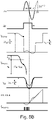
- Fig. 5B illustrates various signals used for explaining the first approach using a voltage across capacitor 111 as the measure.
- I ZVS is the current through the zero voltage switching transistor 18, as already represented as curve 51 in Fig. 4A .
- GD1 is the control signal for the zero voltage switching transistor, where an on-time is adapted according to techniques discussed herein.
- V DS.ZVS denotes a drain source voltage of zero voltage switching transistor 18. As indicated in Fig. 5B , the amplitude of this voltage depends on the input voltage V IN and the winding ratio N Z /N P , wherein a maximum value is V IN (N Z /N P ).
- VDS.main denotes a drain source voltage of the primary transistor switch, like primary transistor switch 15 of Fig. 1 . This voltage is reduced by the action of the zero voltage switch circuit part before the primary transistor switch is switched on.
- V OR is the output voltage Vout refelcted back to the primary side via transformer 12.
- I DRAIN.MAIN is a current through the primary transistor switch.
- V CZ is the voltage across capacitor 111.
- the voltage starts at V IN (N Z /N P ), then drops ad then rises again.
- a minimum of V CZ corresponds to the boundary between regions (A) and (B). Therefore, a time duration between switching on the zero voltage switching transistor and this minimum corresponds to half the period of the current I ZVS through zero voltage switching transistor 18. Consequently, V CZ may serve as a measure of the period of the current through zero voltage switching transistor 18.
- a counter may start at the switching on of the zero voltage switching transistor, and stop when the minimum of the V CZ is reached.
- the derivative dV CZ /dt with respect to time or an approximation thereof may be continuously calculated, and when the derivative is below a predefined value (at or close to zero), this may be seen as the minimum being reached.
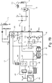
- Fig. 5C is a circuit diagram illustrating a controller 51 adapted for controlling the zero voltage switching transistor 18 with a signal GD1 and a primary transistor switch like primary transistor switch 15 of Fig. 1 with a signal GD0 based on sensing the voltage V CZ .
- Fig. 5C shows the zero voltage switch circuit part already discussed with reference to Fig. 5A , with components 18, 19, 110, 111 and 50.
- the voltage V CZ across capacitor 111 is received by controller 51 at an input terminal also labeled V CZ .
- Controller 51 includes a first driver 52, in the example shown a push-pull driver for driving zero voltage switching transistor 18 with signal GD1, and a second driver 53 for driving a primary transistor switch like primary transistor switch 50 of Fig. 1 with a signal GD0.
- controller 51 receives a supply voltage VCC derived from first auxiliary winding 112, and further receives a voltage ZCD derive from a voltage at first auxiliary winding 112 via a resistive divider, as shown.
- the voltage received at input ZCD is indicative of the drain source voltage of the primary transistor switch, V DS.MAIN in Fig. 5B .
- a valley in voltage received at input ZCD which corresponds to the point V IN -V OR in V DS.MAIN , is detected by a valley sensing 516, which may be implemented in a conventional manner, for example by monitoring the slope of the received signal.
- valley sensing 516 When a valley is detected by valley sensing 516 a corresponding signal is provided to a control logic 55 that controls first and second drivers 52, 53.
- the receipt of the signal from valley sensing 516 by control logic 55 causes control logic 55 to control first driver 51 to switch zero voltage switching transistor 18 on, and with a delay T SHIFT caused by a delayed block 54 control second driver 53 to switch the primary transistor switch like primary transistor switch 15 of Fig. 1 on.
- the signal from valley sensing 116 switches an oscillator 510 on, which generates a clock signal with a frequency fs clocking a counter 59 and an analog to digital converter (ADC) 58.
- ADC analog to digital converter
- the signal from valley sensing 516 is provided to a set input of a set/reset flip-flop 511. This starts counting of counter 59 with frequency fs.
- the frequency fs may be set by controller 17 or 20 based on feedback from the secondary side, e.g. at terminal MFIO aif controller
- the voltage V CZ is provided to an analog to digital converter (ADC) 58 for conversion to digital value.
- ADC analog to digital converter
- 8 bit values are indicated (bits 0 to 7), but this is merely an example. Any suitable analog to digital converters like tracking analog to digital converters or sigma delta analog to digital converters may be used.
- the converted value of V CZ is stored in a register 512.
- this value from register 512 is provided to an input (B) of a subtractor 514, and an actual value (one clock cycle later than the value stored in register 512) is provided to an input (A) of subtractor 514.
- n-th value output by ADC 58 is provided to input (A) of subtractor 514, and the previous (n-1)-th value is provided to input (B) of subtractor 514.
- Subtractor 514 calculates the difference between the values, for example the (n-1)-th value minus the n-th value, and feeds the output to an input (B) of a digital comparator 514. In this way, subtractor 514 approximates a value for the derivative dV CZ /dt, by calculating the difference for one clock period. This is illustrated in a curve 517, where this difference is shown for two instances.
- the digital comparator 514 compares the signal received from subtractor 514 with a constant 515 received at an input (A) of digital comparator 514. When the output from subtractor 514 is below the constant, this is taken as an indication that the valley of V CZ has been reached. In other words, the constant is a small value, which when reached, indicates that the slope of the V CZ has essentially reached zero. When this is the case, digital comparator 514 outputs a signal to a reset input R of set/reset flip-flop 514.
- An output Q of set/reset flip-flop 511 is coupled to an enable input of counter 59.
- valley sensing 516 applies a signal to the set input of set/reset flip-flop 511, this causes counter 59 to be enabled and to start counting.
- Application of the signal from digital comparator 513 to reset input R of set/reset flip-flop 511 causes output Q to toggle and therefore to stop counting of counter 59. Therefore, counter 59 then outputs the time from switching on zero voltage switching transistor 18 to the valley of V CZ in terms of clock periods of clock signal CLK, which time, as can be seen in Fig. 5B , corresponds to half the period of I ZVS .
- the counting of counter 59 symbolized by signal T POSI.ZVS in Fig. 5D .
- the value thus output by counter 59 is stored in register 57 and multiplied by a factor in a multiplier 56.
- a multiplication by 2 would corresponds to the full period of I ZVS .
- the factor may be chosen slightly lower than 2, for example 1.9 in Fig. 5C .
- the result of multiplier 56 is provided to control logic 55, which controls first driver 52 to switch off zero voltage switching transistor 18 off after the time T GD1 indicated by the output of multiplier 56. In this way, the on-time of zero voltage switching transistor 18 is set to almost the full period of I ZVS , and can be adapted to variations due to processing variations, temperature variations, parasitic capacitances, etc.
- controller 51 for measuring the time from switching on of zero voltage switching transistor 18 to the valley based on V CZ is merely an example, and other circuits also may be used.
- elements downstream of analog to digital converter 58 like register 512, subtractor 514, digital comparator 514, etc. it may be implemented in hardware, but also may be implemented in software processing digital values.
- the determination may be turned off. This turn-off may deactivate the counter for GD1 when a voltage V DS.ZVS reaches its valley, or may deactivate the counter 59 after the measurement, i.e.
- the measurement may therefore be deactivated for the other half period.
- Figs. 6A to 6C a further example for a measure for the period of I ZVS will be discussed, referring to Figs. 6A to 6C .
- some elements in the embodiments of Figs. 6A to 6C are similar to the embodiment of Fig. 5A to 5C , bear the same reference numerals and therefore will not be described in full detail again.
- the measurement is based on the voltage V CZ .
- the voltage is not used directly, but a capacitive divider is used to obtain a measure of the period of I ZVS .
- Fig. 6A shows a zero voltage switch circuit part according to a corresponding embodiment.
- the zero voltage switch part of Fig. 6A includes components 18, 19, 110 and 111 are already discussed.
- Parallel to capacitor 111 a capacitive divider including a first capacitor 60 and a second capacitor 61 couples in series, with a resister 62 coupled in parallel to second capacitor 61, is provided.
- a node between first capacitor 60 and second capacitor 61 is coupled to a terminal 63, at which the divider voltage as a measure for the period of I ZVS may be tapped.
- capacitor 111 may have a capacitance of about 10nF
- first capacitor 60 may have a capacitance of about 68pF
- second capacitor 61 may have a capacitance of about 4.7nF
- resistor 62 may have a resistance value of 1 Ohm.
- Other values are also possible.
- a capacitance value of the series connection between first and second capacitor 60, 61 is at least one order of magnitude, for example about two orders of magnitude, smaller than the capacitance of capacitor 111, as in the numerical example above, which conversely means that an impedance of a path via capacitor 111 is significantly smaller than an impedance of a path via the capacitive divider including first and second capacitors 60, 61 and resistor 62.
- This in turn means that a current indicated by an arrow 64 through capacitor 111 is significantly larger than a current indicated by an arrow 65 through the capacitive divider, which in turn means that the influence of the capacitive divider on the operation of the zero voltage switch circuit part shown is low.
- Fig. 6B illustrates example signals for the currently discussed embodiment using a capacitive divider. Most of the signals have already been explained with reference to Fig. 5B and have the same designations.
- Fig. 6B shows a voltage V CAP.DIVIDER , which is an example voltage at terminal 63 of Fig. 6A .
- the voltage has an oscillating behavior, with a sign opposite to I ZVS .
- a time from switching on zero voltage switching transistor 18 until the voltage V CAP.DIVIDER crossing 0, i.e. transitioning from negative to positive, or in other words V CAP.DIVIDER becoming positive may be detected detected. This time period may be measured by a counter in terms of clock signals, as indicated by T POSI.ZVS , and the time corresponds to half the period of I ZVS .
- Fig. 6C illustrates a controller 66 implemented for taking an output voltage of a capacitive divider as a measure of the period of I ZVS .
- controller 66 receives a supply voltage from first auxiliary winding 112 and receives the voltage ZCD from the resistive divider coupled to first auxiliary winding 112, and performs a valley sensing 516, which using control logic 55 switches zero voltage switching transistor 18 on by controlling first driver 52 accordingly, and switching a primary transistor switch on using second driver 53 with a time delay 54.
- valley sensing 516 switches oscillator 510 for providing a clock signal on, and applies a signal to a set input S of set/reset flip-flop 511 already described, which starts counting of counter 59.
- ADC 58 in this case receive the signal from the capacitive divider of the zero voltage switch part already shown in Fig. 6A and reproduced in Fig. 6C at an input ZVS. The resulting digital value is compared to a constant 515 in a digital comparator 513.
- the constant 515 may be zero or close to zero, to detect when the voltage output by the capacitive divider becomes positive.
- the output of digital comparator 513 is provided to a reset input R of set/reset flip-flop 511 to stop counting of counter 59.
- the output of counter 59 measures half the period of I ZVS in terms of clock periods of the clock signal generated by oscillator 510.
- the output of counter 59 is then processed as in Fig. 5C using register 57 and multiplier 56.
- the output by the capacitive divider may be taken as a measure of the period I ZVS .
- FIGs. 7A and 7B A further embodiment illustrating a further measure which may be used is illustrated in Figs. 7A and 7B .
- the drain source voltage of the zero voltage switching transistor is used as a measure of the period of I ZVS .
- essentially the same zero voltage switch circuit part as shown in Fig. 5A including diode 50 may be used, which therefore will not be reproduced again.
- Fig. 7A reproduces the signals shown in Fig. 5B .
- the focus is on the voltage V DS.ZVS .
- this voltage during the period of I ZVS exhibits a similar oscillation, with a zero crossing from positive to negative at the transition between areas (A) and (B).
- the zero voltage switching transistor therefore may only be switched off while V DS.ZVS is negative.
- Half a period of I ZVS may be measured by measuring the time from switching on the zero voltage switching transistor to V DS.ZVS becoming negative.
- Fig. 7B shows a diagram of a controller 70 adapted to use the drain source voltage of zero voltage switching transistor 18 as a measure for the time period of I ZVS . Similar to Fig. 6C , elements already described with reference to Figs. 5C or 6C bear the same reference numerals and will not be discussed again in detail. For instance, also controller 70 receives a supply voltage from first auxiliary winding 112 and includes valley sensing 516 based on which oscillator 510 is switched on, zero voltage switching transistor 18 and a primary transistor switch like primary transistor switch 15 of Fig. 1 are switched on via first and second drivers 52, 52 by control logic 55 using delay 54 for switching on the primary transistor switch, and valley sensing 516 furthermore applies a signal to a set input of set/reset flip-flop 511 starting counter 59.
- controller 17 receives a voltage V DS from a node between zero voltage switching transistor 18 and second auxiliary winding 19, which corresponds to the drain source voltage of zero voltage switching transistor 18 with respect to ground.
- V TH is selected to be smaller than V IN x N Z /N P as in Fig. 7A , such that the actual detection and sensing only occurs in the phase when the drain source voltage is at low value in the oscillating part in Fig. 8A.
- Comparator 71 may save power by turning on oscillator
- V DS.ZVS is then digitized by analog to digital converter 58.
- the thus digitized value is compared to a constant 515 in digital comparator 513 to detect when V DS.ZVS becomes negative. Therefore, threshold 515 may be at or close to zero.
- threshold 515 may be at or close to zero.
Landscapes
- Engineering & Computer Science (AREA)
- Power Engineering (AREA)
- Dc-Dc Converters (AREA)
Abstract
Description
- The present application relates to controllers for forward mode current injection (FMCI) converters, FMCI converters and corresponding methods.
- Power converters are generally used to convert an input electrical power (voltage, current) to an output electrical power (voltage, current) and may for example operate as voltage converter to convert an input voltage like a mains voltage to an output voltage required by a specific load.
- One class of power converters are switched mode power supplies (SMPS), where a primary side switch is operated to selectively provide power ultimately to an output of the converter. Some types of SMPS use a galvanic isolation provided by a transformer, where the primary side switch selectively provides power to a primary winding of a transformer, with a secondary winding of the transformer being coupled to an output of the SMPS. As primary side switches in SMPS, frequently transistors like metal oxide semiconductor field effect transistors (MOSFETS) or other transistor types are used.
- In this case, often so called zero voltage switching (ZVS) is employed, where a switching of the primary side switch from an off-state to an on-state is performed at a time where only a comparatively small voltage, ideally zero volt, but in practical implementations sometimes some few volts, is applied across the primary side switch, for example between source and drain terminals in case of a MOSFET.
- Different approaches to establish such a zero voltage switching are conventionally known. In forward mode current injection converters, an auxiliary switch, referred to as zero voltage switching transistor herein, is coupled to an auxiliary primary side winding of the transformer and to a capacitor, and is switched on shortly before the primary side switch is switched on to establish zero voltage switching.
- A controller as defined in
claim 1, a forward mode current injection converter as defined in claim 8 and a method as defined inclaim 12 are provided. The dependent claims define further embodiments. - According to an embodiment, a controller for a forward mode current injection converter is provided, comprising:
- an input to receive a measure of a period of a current through a zero voltage switching transistor of the forward mode current injection converter, and
- control logic configured to set an on-time of the zero voltage switching transistor based on the measure.
- In another embodiment, a forward mode current injection converter including such a controller as provided.
- According to a further embodiment, a method for controlling a forward mode current injection converter is provided, comprising:
- receiving a measure of a period of a current through a zero voltage switching transistor of the forward mode current injection converter,
- setting an on-time of the zero voltage switching transistor based on the measure.
- The above summary is merely intended to provide a brief overview over some embodiments and is not to be construed as limiting, as other embodiments may include other features than the ones given above.
-
-
Fig. 1 is a circuit diagram of a forward mode current injection converter according to some embodiments. -
Fig. 2 is a block diagram illustrating a controller according to some embodiments. -
Fig. 3 is a flow chart illustrating a method according to some embodiments. -
Figs. 4A to 4C are diagrams illustrating different operation phases of a zero voltage switching transistor. -
Figs. 5A to 5C are diagrams illustrating some embodiments. -
Figs. 6A to 6C are diagrams illustrating some embodiments. -
Figs. 7A and7B are diagrams illustrating some embodiments. - In the following, various embodiments will be described in detail referring to the attached drawings. These embodiments are given as examples only and are not to be construed as limiting in any way. For example, while embodiments may be described comprising a plurality of features (components, circuit elements, acts, events, steps, etc.), in other embodiments some of the features may be omitted, and/or may be replaced by alternative features or elements. In addition to the features explicitly described, further features may be provided. For example, embodiments discussed herein relate to setting an on-time for a zero voltage switching transistor of a forward mode current injection (FMCI) converter. Apart from this setting of an on-time, the FMCI converter may be implemented in any conventional manner, and such conventional implementation details will not be described here in detail.
- Different embodiments may be combined with each other to form further embodiments unless noted otherwise. Variations and modifications described with respect to one of the embodiments may also be applicable to other embodiments and will therefore not be described repeatedly.
- In the embodiments shown and described, any direct electrical connection or coupling between elements, i.e. connections or couplings without intervening elements, may be replaced by an indirect connection or coupling, i.e. connection or coupling comprising one or more additional intervening elements, and vice versa, as long as the general purpose of the connection or coupling, for example to provide a certain kind of signal, a certain kind of information or a certain kind of control, is essentially maintained. In other words, connections or couplings may be modified as long as the general purpose and function of the connection or coupling remains essentially unaltered.
- Embodiments discussed herein use transistors as switches. While in embodiments discussed here in metal oxides semiconductor field effect transistors (MOSFETS) are used as examples, in other embodiments other kinds of transistors, for example bipolar junction transistors (BJTs) or insulated gate bipolar transistors (IGBTs), may be used. Transistors may be based on different semiconductor materials like silicon, silicon carbide or III-V semiconductors like gallium arsenide or gallium nitride. A switch, for example transistor, is on or closed when it provides a low ohmic connection between terminals thereof (source and drain terminals or collector and emitter terminals), and it is described as off or open in a state where it provides essentially an electric isolation between the terminals (apart possibly from some undesired leaked currents, which are generally orders of magnitudes lower than currents in the on state).
- Any signals shown in the drawings or values given for components like resistance values, capacitance values etc., are to be taken merely as examples, as actual signal waveforms may vary depending on a particular implementation, and values for components may be changed.
- Turning now to the figures,
Fig. 1 is a circuit diagram of a forward mode current injection (FMCI) converter according to an embodiment. Apart from a control of an on-time of a zerovoltage switching transistor 18 by acontroller 17, the FMCI converter ofFig. 1 may be implemented in any conventional manner, and the configuration shown is only an example. Therefore, the converter ofFig. 1 will be described comparatively briefly below. - The FMCI converter of
Fig. 1 includes aprimary side 10 and asecondary side 11 separated by atransformer 12. In the example ofFig. 1 ,primary side 10 receives an AC input voltage VAC, for example a mains voltage, which is rectified and filtered to provide a voltage VIN. Aprimary transistor switch 15, when switched on, causes a current flow through a primary side winding 13 oftransformer 12, which transfers energy to a secondary side winding 14 oftransformer 12, which provides an output voltage Vout at anoutput capacitor 113. Primaryside transistor switch 15 is controlled by a control signal GD0 from acontroller 17. A feedback network provides feedback of the output voltage via anoptocoupler primary transistor switch 15 to establish a desired output voltage Vout. - Furthermore, a first
auxiliary winding 112 on the primary side on the one hand serves for providingcontroller 17 with power at a VCC input and further provides information regarding a current through the transformer/primaryside transistor switch 15 at an input ZCD ofcontroller 17. - A second
auxiliary winding 19, aninductor 110 and a capacitor 111 (also referred to as Cz) form a resonant circuit, in which a zerovoltage switching transistor 18 is provided. Secondauxiliary winding 19, as indicated by the dot, has the same winding direction as primary side winding 13, whereas firstauxiliary winding 112 and secondary side winding 14 have the opposite winding direction ofprimary winding 13. Zerovoltage switching transistor 18 is switched on shortly beforeprimary transistor switch 15 is switched on in each switching cycle. The energy injection throughauxiliary winding 19 then causes zero voltage switching when switching onprimary transistor switch 15. The time when the zerovoltage switching transistor 18 is switched on may depend on a mode the converter is operated and may for example be at valley of a drain source voltage of theprimary transistor switch 15, which may be measured at input ZCD inFig. 7 based on a signal from firstauxiliary winding 112, or may be with a fixed frequency. - NP, NA, NZ and NS denote a number of winding of 13, first
auxiliary winding 112, secondauxiliary winding 19 andsecondary winding 14, respectively. - As described so far, the embodiment of
Fig. 1 and operation thereof corresponds to a conventional operation of an FMCI converter and will therefore not be described in more detail. - As will be explained below in more detail, in conventional solutions zero
voltage switching transistor 18, after being turned on, remains turned on for a preconfigured, fixed time. In various embodiments discussed herein, instead of that,controller 17 receives a measure of a period of a current through zerovoltage switching transistor 18. A measure of a period of a current refers to any value, signal or quantity which includes information regarding a time duration of a period of the current through zerovoltage switching transistor 18. Various examples for such a measure will be discussed below in more detail. The time during which the zerovoltage switching transistor 18 is switched on, also referred to as on-time of zerovoltage switching transistor 18, is then determined bycontroller 17 based on this measure, and zerovoltage switching transistor 18 is controlled accordingly. Also for this, more detailed examples will be given further below. - For further illustration,
Fig. 2 shows acontroller 20 according to an embodiment. Only parts ofcontroller 20 relevant to the control of zerovoltage switching transistor 18 are shown, and other parts ofcontroller 20 may be implemented in any conventional manner. -
Controller 20 includes a terminal 21 configured to receive a measure meas of the period of the current through a zero voltage switching transistor from a zero voltageswitch circuit part 24. In the example ofFig. 1 , zero voltageswitch circuit part 24 includescomponents control logic 24 processes this measure meas and controls a zero voltage switching transistor of thecircuit part 24 using a signal GD1 accordingly, with a corresponding on-time based on the measure. -
Fig. 3 is a flow chart illustrating a method according to an embodiment, which may be implemented incontroller 20 ofFig. 2 orcontroller 17 ofFig. 1 , and for ease of explanation will be described referring to thedescription 1 and 2 above. At 30, the method ofFig. 3 comprises receiving a measure of a period of a current through a zero voltage switching transistor, like zerovoltage switching transistor 18 ofFig. 1 . At 31, the method includes setting an on-time of the zero voltage switching transistor based on the measure. The method ofFig. 3 may for example be performed bycontrol logic 21, which may include hardware components to perform the method. Examples for such hardware components will be described below. In other embodiments, the method may also be fully or partially implemented in software running on a controller like a programmable micro controller. - Next, conditions for setting the on-time of a zero voltage switching transistor like
transistor 18 inFig. 1 will be discussed referring toFig. 4 , including subfigures 4A to 4C.Fig. 4A shows example signals,Fig. 4B shows a current in an area (C) ofFig. 4 in a zero voltage switch circuit part, andFig. 4C shows a current in an area (D) ofFig. 4 . - As an example for a zero voltage switch part, in
Figs. 4B and4C the corresponding circuit parts ofFig. 1 including zerovoltage switching transistor 18, second auxiliary winding 19,inductor 110 andcapacitor 111 is used. - A
curve 31 inFig. 1 shows a current Izvs through zerovoltage switching transistor 18. Upon switching on zerovoltage switching transistor 18, first due to stored energy in the resonant circuit formed bycapacitor 111, second auxiliary winding 19 andinductor 110, a positive half wave of the current Izvs occurs in a region (A). A positive current, in this respect, is a current fromcapacitor 111 throughinductor 110 and auxiliary secondary winding 19 and then back tocapacitor 111 through zerovoltage switching transistor 18, and a negative current as a current in the opposite direction, as shown inFig. 4D for a negative current andFig. 4C for a positive current. Then, the current IZVS becomes negative in a quarter wave in an area (B) and a further quarter wave in an area (C), before becoming positive again in an area (D). - An on-time of the zero
voltage switching transistor 18 which extends into area (D), as shown as an example in acurve 40 illustrating a control signal GD1 extending to area (D), is undesirable for reason illustrated inFig. 4C . Here, a positive current flows through zerovoltage transistor 18 being switched on, causing a rise of the drain source voltage VDS.ZVS of zerovoltage switching transistor 18. This, as indicated by inFig. 4C , may cause a voltage spike at a secondary side of the FMCI converter, for example as at a synchronal rectifying (SR)method 44 on the secondary side, through induction in secondary winding 14. Such voltage spikes may damage e.g. asynchronous rectifier MOSFET 44 or require a stronger design ofsynchronous rectifier MOSFET 44, which increases costs. The voltage spike occurring is related to charging the intrinsic capacitances of the zero voltage switching transistor if the zero voltage switching transistor is turned off while IZVS is positive. The spike explained here forsynchronous rectifier MOSFET 44 may also occur at other rectifying elements, for example a rectifyingdiode 114 onsecondary side 11 shown inFig. 1 . In contrast, if the zero voltage switching transistor is switched off while IZVS is negative, no such spike occurs - In conventional solutions, a fixed duration of the on-time of zero
voltage switching transistor 18 is used, which may be pre-programmed in a respective controller. Such an on-time as illustrated by acurve 42 inFig. 4A showing a control signal GD1 causing a fixed on-time. In some conventional approaches, the on-time is set to end nominally at the boundary between areas (B) and (C), i.e. at the minimum of IZVS. "Nominally" means that this time is set for nominal values of various circuit components like capacitates ofcapacitor 111, inductances ofinductors voltage switching transistor 18 etc. This choice provides a safety margin against the current reaching area (D). In particular, the period length of IZVS varies with variations of the above mentioned values like capacitance value ofcapacitor 111, inductance values ofinductors - On the other hand, this has the disadvantage that the zero
voltage switching transistor 18 is switched off at least during most of area (C) and possibly also some of area (B), depending on the above mentioned variations. This in turn means that a body diode has to be provided to zerovoltage switching transistor 18 either as an intrinsic diode or as an additional freewheeling diode by design, through which current may flow for example in area (C) when zerovoltage switching transistor 18 is switched off. Current conduction through a body diode generally generates more losses than conduction through switched on zerovoltage switching transistor 18. - Therefore, in embodiments, as already briefly explained referring to
Figs. 1 to 3 , a period of the current IZVS is obtained, and the on-time is adapted based on the measure. In this way, variations of the period may be taken into account, the on-time may be extended essentially to the boundary between areas (C) and (D), as illustrated by acurve 43 inFig. 4A showing an example adaptive control signal GD1. For example, the on-time may be set to the full period length (2 half periods), possibly minus a safety margin like minus 5% or minus 10% or minus a fixed time to ensure that the zero voltage switching transistor is securely switched off at the beginning of area (D). - In a first approach, to obtain a measure of the period of the current through the zero voltage switching transistor, a voltage across a capacitor of the zero voltage switch circuit part used is monitored, in the example of
Fig. 1 capacitor 111. This will be explained referring toFig. 5 including subfigures 5A to 5C. -
Fig. 5A shows a corresponding zero voltage switch circuit part for this approach. In addition tocomponents diode 50 is additionally provided, which allows current flow in case of a positive current IZVS (for definitions of positive and negative current, see the explanations above with reference toFig. 4B and4C ). In other words, thediode 50 provides negative clamping. In some implementations, this helps to avoid negative voltages at a terminal of a controller that receives the voltage acrosscapacitor 111 as the measure. For sufficiently large capacitances ofcapacitor 111, the voltage acrosscapacitor 111 usually does not drop below 0 (e.g. VSS), and insuch implementations diode 50 may be omitted. Otherwise, if in some conditions the voltage may drop below 0 withoutdiode 50,diode 50 prevents this by clamping the voltage accordingly. -
Fig. 5B illustrates various signals used for explaining the first approach using a voltage acrosscapacitor 111 as the measure. InFig. 5B , IZVS is the current through the zerovoltage switching transistor 18, as already represented ascurve 51 inFig. 4A . GD1 is the control signal for the zero voltage switching transistor, where an on-time is adapted according to techniques discussed herein. - VDS.ZVS denotes a drain source voltage of zero
voltage switching transistor 18. As indicated inFig. 5B , the amplitude of this voltage depends on the input voltage VIN and the winding ratio NZ/NP, wherein a maximum value is VIN(NZ/NP). - VDS.main denotes a drain source voltage of the primary transistor switch, like
primary transistor switch 15 ofFig. 1 . This voltage is reduced by the action of the zero voltage switch circuit part before the primary transistor switch is switched on. VOR is the output voltage Vout refelcted back to the primary side viatransformer 12.
IDRAIN.MAIN is a current through the primary transistor switch. - Of particular interest to the measure discussed here with reference to
Figs. 5A to 5C is VCZ, which is the voltage acrosscapacitor 111. The voltage starts at VIN(NZ/NP), then drops ad then rises again. A minimum of VCZ, as can be seen inFig. 5B , corresponds to the boundary between regions (A) and (B). Therefore, a time duration between switching on the zero voltage switching transistor and this minimum corresponds to half the period of the current IZVS through zerovoltage switching transistor 18. Consequently, VCZ may serve as a measure of the period of the current through zerovoltage switching transistor 18. For example, as indicated by a signal TPOSI.ZVS, a counter may start at the switching on of the zero voltage switching transistor, and stop when the minimum of the VCZ is reached. To detect the minimum, the derivative dVCZ/dt with respect to time or an approximation thereof may be continuously calculated, and when the derivative is below a predefined value (at or close to zero), this may be seen as the minimum being reached. -
Fig. 5C is a circuit diagram illustrating acontroller 51 adapted for controlling the zerovoltage switching transistor 18 with a signal GD1 and a primary transistor switch likeprimary transistor switch 15 ofFig. 1 with a signal GD0 based on sensing the voltage VCZ .Fig. 5C shows the zero voltage switch circuit part already discussed with reference toFig. 5A , withcomponents capacitor 111 is received bycontroller 51 at an input terminal also labeled VCZ. Controller 51 includes afirst driver 52, in the example shown a push-pull driver for driving zerovoltage switching transistor 18 with signal GD1, and asecond driver 53 for driving a primary transistor switch likeprimary transistor switch 50 ofFig. 1 with a signal GD0. - Furthermore, as already explained briefly with respect to
Fig. 1 ,controller 51 receives a supply voltage VCC derived from first auxiliary winding 112, and further receives a voltage ZCD derive from a voltage at first auxiliary winding 112 via a resistive divider, as shown. - The voltage received at input ZCD is indicative of the drain source voltage of the primary transistor switch, VDS.MAIN in
Fig. 5B . A valley in voltage received at input ZCD, which corresponds to the point VIN-VOR in VDS.MAIN, is detected by avalley sensing 516, which may be implemented in a conventional manner, for example by monitoring the slope of the received signal. - When a valley is detected by valley sensing 516 a corresponding signal is provided to a
control logic 55 that controls first andsecond drivers valley sensing 516 bycontrol logic 55 causes controllogic 55 to controlfirst driver 51 to switch zerovoltage switching transistor 18 on, and with a delay TSHIFT caused by a delayedblock 54 controlsecond driver 53 to switch the primary transistor switch likeprimary transistor switch 15 ofFig. 1 on. Furthermore the signal from valley sensing 116 switches anoscillator 510 on, which generates a clock signal with a frequency fs clocking acounter 59 and an analog to digital converter (ADC) 58. Finally, the signal fromvalley sensing 516 is provided to a set input of a set/reset flip-flop 511. This starts counting ofcounter 59 with frequency fs. The frequency fs may be set bycontroller controller 17, to measure the period as explained below with sufficent resolution. - The voltage VCZ is provided to an analog to digital converter (ADC) 58 for conversion to digital value. As an example, in
Fig. 5C in various instances 8 bit values are indicated (bits 0 to 7), but this is merely an example. Any suitable analog to digital converters like tracking analog to digital converters or sigma delta analog to digital converters may be used. For each clock period, the converted value of VCZ is stored in aregister 512. In a next clock period, this value fromregister 512 is provided to an input (B) of asubtractor 514, and an actual value (one clock cycle later than the value stored in register 512) is provided to an input (A) ofsubtractor 514. In other words, in an n-th clock cycle the n-th value output byADC 58 is provided to input (A) ofsubtractor 514, and the previous (n-1)-th value is provided to input (B) ofsubtractor 514.Subtractor 514 calculates the difference between the values, for example the (n-1)-th value minus the n-th value, and feeds the output to an input (B) of adigital comparator 514. In this way,subtractor 514 approximates a value for the derivative dVCZ/dt, by calculating the difference for one clock period. This is illustrated in acurve 517, where this difference is shown for two instances. - The
digital comparator 514 compares the signal received fromsubtractor 514 with a constant 515 received at an input (A) ofdigital comparator 514. When the output fromsubtractor 514 is below the constant, this is taken as an indication that the valley of VCZ has been reached. In other words, the constant is a small value, which when reached, indicates that the slope of the VCZ has essentially reached zero. When this is the case,digital comparator 514 outputs a signal to a reset input R of set/reset flip-flop 514. - An output Q of set/reset flip-
flop 511 is coupled to an enable input ofcounter 59. Whenvalley sensing 516 applies a signal to the set input of set/reset flip-flop 511, this causes counter 59 to be enabled and to start counting. Application of the signal fromdigital comparator 513 to reset input R of set/reset flip-flop 511 causes output Q to toggle and therefore to stop counting ofcounter 59. Therefore, counter 59 then outputs the time from switching on zerovoltage switching transistor 18 to the valley of VCZ in terms of clock periods of clock signal CLK, which time, as can be seen inFig. 5B , corresponds to half the period of IZVS. The counting ofcounter 59 symbolized by signal TPOSI.ZVS inFig. 5D . The value thus output bycounter 59 is stored inregister 57 and multiplied by a factor in amultiplier 56. A multiplication by 2 would corresponds to the full period of IZVS. To provide some safety margin as explained above, the factor may be chosen slightly lower than 2, for example 1.9 inFig. 5C . The result ofmultiplier 56 is provided to controllogic 55, which controlsfirst driver 52 to switch off zerovoltage switching transistor 18 off after the time TGD1 indicated by the output ofmultiplier 56. In this way, the on-time of zerovoltage switching transistor 18 is set to almost the full period of IZVS, and can be adapted to variations due to processing variations, temperature variations, parasitic capacitances, etc. - It should be noted that the circuit shown in
controller 51 for measuring the time from switching on of zerovoltage switching transistor 18 to the valley based on VCZ is merely an example, and other circuits also may be used. For instance, elements downstream of analog todigital converter 58, likeregister 512,subtractor 514,digital comparator 514, etc. it may be implemented in hardware, but also may be implemented in software processing digital values. Moreover, as indicated, by applying signals "turn off" to register 57 and to a node betweendigital comparator 514 and set/reset flip-flop 511, the determination may be turned off. This turn-off may deactivate the counter for GD1 when a voltage VDS.ZVS reaches its valley, or may deactivate thecounter 59 after the measurement, i.e. when the counting has stopped, for the remaining resonant period (e.g. essentially after area (A)). In implementations like the one ofFig. 5 or implementations discussed below where essentially half the period of the current is measured, the measurement may therefore be deactivated for the other half period. - Next, a further example for a measure for the period of IZVS will be discussed, referring to
Figs. 6A to 6C . As will be seen, some elements in the embodiments ofFigs. 6A to 6C are similar to the embodiment ofFig. 5A to 5C , bear the same reference numerals and therefore will not be described in full detail again. - Also in the case of
Fig. 6A to 6C the measurement is based on the voltage VCZ. However, in this case, the voltage is not used directly, but a capacitive divider is used to obtain a measure of the period of IZVS. -
Fig. 6A shows a zero voltage switch circuit part according to a corresponding embodiment. - The zero voltage switch part of
Fig. 6A includescomponents capacitor 111, a capacitive divider including afirst capacitor 60 and asecond capacitor 61 couples in series, with aresister 62 coupled in parallel tosecond capacitor 61, is provided. A node betweenfirst capacitor 60 andsecond capacitor 61 is coupled to a terminal 63, at which the divider voltage as a measure for the period of IZVS may be tapped. To give example values,capacitor 111 may have a capacitance of about 10nF,first capacitor 60 may have a capacitance of about 68pF,second capacitor 61 may have a capacitance of about 4.7nF, andresistor 62 may have a resistance value of 1 Ohm. Other values are also possible. - In embodiments, a capacitance value of the series connection between first and
second capacitor capacitor 111, as in the numerical example above, which conversely means that an impedance of a path viacapacitor 111 is significantly smaller than an impedance of a path via the capacitive divider including first andsecond capacitors resistor 62. This in turn means that a current indicated by anarrow 64 throughcapacitor 111 is significantly larger than a current indicated by anarrow 65 through the capacitive divider, which in turn means that the influence of the capacitive divider on the operation of the zero voltage switch circuit part shown is low. -
Fig. 6B illustrates example signals for the currently discussed embodiment using a capacitive divider. Most of the signals have already been explained with reference toFig. 5B and have the same designations. In addition to the signals ofFig. 5B ,Fig. 6B shows a voltage VCAP.DIVIDER, which is an example voltage atterminal 63 ofFig. 6A . As can be seen, the voltage has an oscillating behavior, with a sign opposite to IZVS. In embodiments, a time from switching on zerovoltage switching transistor 18 until the voltage VCAP.DIVIDER crossing 0, i.e. transitioning from negative to positive, or in other words VCAP.DIVIDER becoming positive, may be detected detected.
This time period may be measured by a counter in terms of clock signals, as indicated by TPOSI.ZVS, and the time corresponds to half the period of IZVS. -
Fig. 6C illustrates acontroller 66 implemented for taking an output voltage of a capacitive divider as a measure of the period of IZVS. Elements having the same function as explained with reference toFigs. 5C bear the same reference numerals. In particular, alsocontroller 66 receives a supply voltage from first auxiliary winding 112 and receives the voltage ZCD from the resistive divider coupled to first auxiliary winding 112, and performs avalley sensing 516, which usingcontrol logic 55 switches zerovoltage switching transistor 18 on by controllingfirst driver 52 accordingly, and switching a primary transistor switch on usingsecond driver 53 with atime delay 54. - Furthermore,
valley sensing 516switches oscillator 510 for providing a clock signal on, and applies a signal to a set input S of set/reset flip-flop 511 already described, which starts counting ofcounter 59. - Furthermore,
ADC 58 in this case receive the signal from the capacitive divider of the zero voltage switch part already shown inFig. 6A and reproduced inFig. 6C at an input ZVS. The resulting digital value is compared to a constant 515 in adigital comparator 513. In this case, the constant 515 may be zero or close to zero, to detect when the voltage output by the capacitive divider becomes positive. As inFig. 5C , the output ofdigital comparator 513 is provided to a reset input R of set/reset flip-flop 511 to stop counting ofcounter 59. Also in this case, the output ofcounter 59 measures half the period of IZVS in terms of clock periods of the clock signal generated byoscillator 510. The output ofcounter 59 is then processed as inFig. 5C using register 57 andmultiplier 56. - Therefore, also the output by the capacitive divider may be taken as a measure of the period IZVS.
- A further embodiment illustrating a further measure which may be used is illustrated in
Figs. 7A and7B . In this approach, the drain source voltage of the zero voltage switching transistor is used as a measure of the period of IZVS. For this, essentially the same zero voltage switch circuit part as shown inFig. 5A including diode 50 may be used, which therefore will not be reproduced again. -
Fig. 7A reproduces the signals shown inFig. 5B . In the currently discussed embodiment, the focus is on the voltage VDS.ZVS. As can be seen, this voltage during the period of IZVS exhibits a similar oscillation, with a zero crossing from positive to negative at the transition between areas (A) and (B). To ensure correct timing, the zero voltage switching transistor therefore may only be switched off while VDS.ZVS is negative. Half a period of IZVS may be measured by measuring the time from switching on the zero voltage switching transistor to VDS.ZVS becoming negative. -
Fig. 7B shows a diagram of acontroller 70 adapted to use the drain source voltage of zerovoltage switching transistor 18 as a measure for the time period of IZVS. Similar toFig. 6C , elements already described with reference toFigs. 5C or6C bear the same reference numerals and will not be discussed again in detail. For instance, alsocontroller 70 receives a supply voltage from first auxiliary winding 112 and includesvalley sensing 516 based on whichoscillator 510 is switched on, zerovoltage switching transistor 18 and a primary transistor switch likeprimary transistor switch 15 ofFig. 1 are switched on via first andsecond drivers control logic 55 usingdelay 54 for switching on the primary transistor switch, andvalley sensing 516 furthermore applies a signal to a set input of set/reset flip-flop 511 startingcounter 59. - Furthermore, for measuring the drain source voltage of zero
voltage switching transistor 18,controller 17 receives a voltage VDS from a node between zerovoltage switching transistor 18 and second auxiliary winding 19, which corresponds to the drain source voltage of zerovoltage switching transistor 18 with respect to ground. - This voltage is compared to a threshold VTH generated by a
voltage source 73 by acomparator 71, and aswitch 74 allowing further processing of the voltage VDS.ZVS by analog todigital converter 58 and following elements is only closed when the voltage VDS.ZVS is below VTH. For example, VTH is selected to be smaller than VIN x NZ/NP as inFig. 7A , such that the actual detection and sensing only occurs in the phase when the drain source voltage is at low value in the oscillating part in Fig. 8A.Comparator 71 may save power by turning on oscillator - The voltage VDS.ZVS is then digitized by analog to
digital converter 58. The thus digitized value is compared to a constant 515 indigital comparator 513 to detect when VDS.ZVS becomes negative. Therefore,threshold 515 may be at or close to zero. As can be seen, due to the phase shift introduced by the capacitive divider, inFig. 6C a transition from negative to positive is to be detected, while inFig. 7B a transition from positive to negative is detected. - The remaining processing is the same as already explained, i.e. the output of
counter 59 is provided to register 57 and multiplied by a factor bymultiplier 56 to determine the on-time for zerovoltage switching transistor 18. - As can be seen from the explanations in
Figs. 5 to 7 , there are various ways of obtaining a measure of the period of the current IZVS through zerovoltage switching transistor 18, and therefore the present application is not limited to any particular method. - Some embodiments are defined by the following examples:
- Example 1. A controller for a forward mode current injection converter, comprising:
- an input configured to receive a measure of a period of a current through a zero voltage switching transistor of the forward mode current injection converter, and
- control logic configured to set an on-time of the zero voltage switching transistor based on the measure.
- Example 2. The controller of example 1, wherein the control logic is configured to set the on-time to within +/-10% of the period of the current.
- Example 3. The controller of example 1 or 2, wherein the control logic is configured to set the on-time to the period of the current minus a predefined safety margin.
- Example 4. The controller of any one of examples 1 to 3, wherein the measure of the period of the current indicates the duration of half of the period of the current.
- Example 5. The controller of any one of examples 1 to 4, wherein the measure indicates a voltage across a capacitor coupled in series with the zero voltage switching transistor, wherein the controller is configured to set the on-time based on a time from switching on of the zero voltage switching transistor until a minimum of the voltage across the capacitor.
- Example 6. The controller of any one of examples 1 to 4, wherein the measure indicates a output voltage of a capacitive divider coupled in parallel to a capacitor that is coupled in series to the zero voltage switching transistor, wherein the controller is configured to set the on-time based on a time between switching on of the zero voltage switching transistor and the output voltage of the capacitive divider becoming positive.
- Example 7. The controller of any one of examples 1 to 4, wherein the measure indicates a voltage across the zero voltage switching transistor, wherein the controller is configured to set the on-time based on a time during which the voltage across the zero voltage switching transistor is positive.
- Example 8. A forward mode current injection converter, comprising:
- a primary transistor switch coupled to selectively provide energy to a primary winding of a transformer, a zero voltage switching transistor coupled to an auxiliary winding on the primary side of the transformer and to a capacitor, and
- the controller of any one of examples 1 to 7 configured to control the primary transistor switch and the zero voltage switching transistor.
- Example 9. The forward mode current injection converter of example 8, wherein the controller is the controller of example 5, and the input of the controller is coupled to the capacitor to receive the voltage across the capacitor as the measure.
- Example 10. The forward mode current injection converter of example 8, wherein the controller is the controller of example 6, wherein the forward mode current injection converter further comprises the capacitive divider in parallel to the capacitor, wherein the input of the controller is coupled to an output of the capacitive divider.
- Example 11. The forward mode current injection converter of example 8, wherein the controller is the controller of example 7, and wherein the input of the controller is coupled to a node between the zero voltage switching transistor and the auxiliary winding.
- Example 12. A method for controlling a forward mode current injection converter, comprising:
- receiving a measure of a period of a current through a zero voltage switching transistor of the forward mode current injection converter, and
- setting an on-time of the zero voltage switching transistor based on the measure.
- Example 13. The method of example 12, wherein setting the on-time comprises setting the on-time to within +/- 10% of the period of the current.
- Example 14. The method of example 12 or 13, wherein setting the on-time comprises setting the on-time to the period of the current minus a predefined safety margin.
- Example 15. The method of any one of examples 12 to 14, wherein the measure of the period of the current indicates the duration of half of the period of the current.
- Example 16. The method of any one of examples 12 to 15, wherein the measure indicates a voltage across a capacitor coupled in series with the zero voltage switching transistor, wherein setting the on-time comprises setting the on-time based on a time from switching on of the zero voltage switching transistor until a minimum of the voltage across the capacitor.
- Example 17. The method of any one of examples 12 to 15, wherein the measure indicates an output voltage of a capacitive divider coupled in parallel to a capacitor that is coupled in series to the zero voltage switching transistor, wherein setting the on-time comprises setting the on-time based on a time between switching on of the zero voltage switching transistor and the output voltage of the divider becoming positive.
- Example 18. The method of any one of examples 12 to 15, wherein the measure indicates a voltage across the zero voltage switching transistor, wherein setting the on-time comprises setting the on-time based on a time during which the voltage across the zero voltage switching transistor is positive.
- Although specific embodiments have been illustrated and described herein, it will be appreciated by those of ordinary skill in the art that a variety of alternate and/or equivalent implementations may be substituted for the specific embodiments shown and described without departing from the scope of the present invention. This application is intended to cover any adaptations or variations of the specific embodiments discussed herein. Therefore, it is intended that this invention be limited only by the claims and the equivalents thereof.
Claims (15)
- A controller (17; 20; 51; 66; 70) for a forward mode current injection converter, comprising:an input (22) configured to receive a measure of a period of a current through a zero voltage switching transistor (18) of the forward mode current injection converter, andcontrol logic (21) configured to set an on-time of the zero voltage switching transistor (18) based on the measure.
- The controller (17; 20; 51; 66; 70) of claim 1, wherein the control logic (21) is configured to set the on-time to within +/- 10% of the period of the current.
- The controller (17; 20; 51; 66; 70) of claim 1 or 2, wherein the control logic (21) is configured to set the on-time to the period of the current minus a predefined safety margin.
- The controller (17; 20; 51; 66; 70) of any one of claims 1 to 3, wherein the measure of the period of the current indicates the duration of half of the period of the current.
- The controller (17; 20; 51; 66; 70) of any one of claims 1 to 4, wherein the measure indicates a voltage across a capacitor (111) coupled in series with the zero voltage switching transistor (18), wherein the controller is configured to set the on-time based on a time from switching on of the zero voltage switching transistor (18) until a minimum of the voltage across the capacitor.
- The controller (17; 20; 51; 66; 70) of any one of claims 1 to 4, wherein the measure indicates a output voltage of a capacitive divider (60, 61) coupled in parallel to a capacitor (111) that is coupled in series to the zero voltage switching transistor (18), wherein the controller is configured to set the on-time based on a time between switching on of the zero voltage switching transistor (18) and the output voltage of the capacitive divider (60, 61) becoming positive.
- The controller (17; 20; 51; 66; 70) of any one of claims 1 to 4, wherein the measure indicates a voltage across the zero voltage switching transistor (18), wherein the controller is configured to set the on-time based on a time during which the voltage across the zero voltage switching transistor (18) is positive.
- A forward mode current injection converter, comprising:a primary transistor switch (15) coupled to selectively provide energy to a primary winding (13) of a transformer (12), a zero voltage switching transistor (18) coupled to an auxiliary winding (19) on the primary side of the transformer (12) and to a capacitor (111), andthe controller (17; 20; 51; 66; 70) of any one of claims 1 to 7 configured to control the primary transistor switch (15) and the zero voltage switching transistor (18).
- The forward mode current injection converter of claim 8, wherein the controller (17; 20; 51; 66; 70) is the controller of claim 5, and the input (22) of the controller is coupled to the capacitor (111) to receive the voltage across the capacitor (111) as the measure.
- The forward mode current injection converter of claim 8, wherein the controller (17; 20; 51; 66; 70) is the controller of claim 6, wherein the forward mode current injection converter further comprises the capacitive divider (60, 61) in parallel to the capacitor (111), wherein the input (22) of the controller (17; 20; 51; 66; 70) is coupled to an output (63) of the capacitive divider (60, 61).
- The forward mode current injection converter of claim 8, wherein the controller (17; 20; 51; 66; 70) is the controller of claim 7, and wherein the input (22) of the controller (17; 20; 51; 66; 70) is coupled to a node between the zero voltage switching transistor (18) and the auxiliary winding (19).
- A method for controlling a forward mode current injection converter, comprising:receiving a measure of a period of a current through a zero voltage switching transistor (18) of the forward mode current injection converter, andsetting an on-time of the zero voltage switching transistor (18) based on the measure.
- The method of claim 12, wherein the measure indicates a voltage across a capacitor (111) coupled in series with the zero voltage switching transistor (18), wherein setting the on-time comprises setting the on-time based on a time from switching on of the zero voltage switching transistor (18) until a minimum of the voltage across the capacitor.
- The method of claim 12 , wherein the measure indicates an output voltage of a capacitive divider (60,61) coupled in parallel to a capacitor (111) that is coupled in series to the zero voltage switching transistor (18), wherein setting the on-time comprises setting the on-time based on a time between switching on of the zero voltage switching transistor (18) and the output voltage of the divider becoming positive.
- The method of claim 12, wherein the measure indicates a voltage across the zero voltage switching transistor (18), wherein setting the on-time comprises setting the on-time based on a time during which the voltage across the zero voltage switching transistor (18) is positive.
Priority Applications (1)
| Application Number | Priority Date | Filing Date | Title |
|---|---|---|---|
| EP21164038.8A EP4064543B1 (en) | 2021-03-22 | 2021-03-22 | Controller for a forward mode current injection converter, forward mode current injection converter and corresponding method |
Applications Claiming Priority (1)
| Application Number | Priority Date | Filing Date | Title |
|---|---|---|---|
| EP21164038.8A EP4064543B1 (en) | 2021-03-22 | 2021-03-22 | Controller for a forward mode current injection converter, forward mode current injection converter and corresponding method |
Publications (2)
| Publication Number | Publication Date |
|---|---|
| EP4064543A1 true EP4064543A1 (en) | 2022-09-28 |
| EP4064543B1 EP4064543B1 (en) | 2025-09-17 |
Family
ID=75143560
Family Applications (1)
| Application Number | Title | Priority Date | Filing Date |
|---|---|---|---|
| EP21164038.8A Active EP4064543B1 (en) | 2021-03-22 | 2021-03-22 | Controller for a forward mode current injection converter, forward mode current injection converter and corresponding method |
Country Status (1)
| Country | Link |
|---|---|
| EP (1) | EP4064543B1 (en) |
Citations (3)
| Publication number | Priority date | Publication date | Assignee | Title |
|---|---|---|---|---|
| US20150194896A1 (en) * | 2014-01-08 | 2015-07-09 | Semiconductor Components Industries, Llc | Method of forming a power supply controller and structure therefor |
| US20180198374A1 (en) * | 2013-05-10 | 2018-07-12 | Rompower Energy Systems, Inc. | True soft switching by timed steering of a current source |
| US20200169180A1 (en) * | 2017-10-12 | 2020-05-28 | Rompower Technology Holdings, Llc | High Efficiency Passive Clamp |
Family Cites Families (1)
| Publication number | Priority date | Publication date | Assignee | Title |
|---|---|---|---|---|
| US8054655B2 (en) * | 2008-11-03 | 2011-11-08 | Monolithie Power Systems, Inc. | Tail current control of isolated converter and apparatus thereof |
-
2021
- 2021-03-22 EP EP21164038.8A patent/EP4064543B1/en active Active
Patent Citations (3)
| Publication number | Priority date | Publication date | Assignee | Title |
|---|---|---|---|---|
| US20180198374A1 (en) * | 2013-05-10 | 2018-07-12 | Rompower Energy Systems, Inc. | True soft switching by timed steering of a current source |
| US20150194896A1 (en) * | 2014-01-08 | 2015-07-09 | Semiconductor Components Industries, Llc | Method of forming a power supply controller and structure therefor |
| US20200169180A1 (en) * | 2017-10-12 | 2020-05-28 | Rompower Technology Holdings, Llc | High Efficiency Passive Clamp |
Also Published As
| Publication number | Publication date |
|---|---|
| EP4064543B1 (en) | 2025-09-17 |
Similar Documents
| Publication | Publication Date | Title |
|---|---|---|
| US11601044B2 (en) | Method for driving an electronic switch in a power converter circuit and control circuit | |
| US10686386B2 (en) | Adaptive synchronous rectifier timing for resonant DC/DC converters | |
| EP3414821B1 (en) | Dc/dc resonant converters and power factor correction using resonant converters, and corresponding control methods | |
| US10516338B2 (en) | Voltage converter controller, voltage converter and method for operating a voltage converter | |
| US7456620B2 (en) | Determining dead times in switched-mode DC-DC converters | |
| US8614568B2 (en) | Gate drive circuit of the voltage drive type semiconductor element and power converter | |
| EP3414824B1 (en) | Dc/dc resonant converters and power factor correction using resonant converters, and corresponding control methods | |
| US9647562B2 (en) | Power conversion with switch turn-off delay time compensation | |
| KR102850933B1 (en) | Flyback converter | |
| US9935547B2 (en) | System and method for a switched-mode power supply | |
| US12301117B2 (en) | Controllers and methods for detecting and adjusting voltage drops related to transistors in power converters | |
| US6055170A (en) | Prediction methods and circuits for operating a transistor as a rectifier | |
| CN111697834A (en) | Controller for closed-loop control of a DCX converter and method thereof | |
| CN113812076A (en) | Mode operation detection for controlling power converter with active clamp switch | |
| US10734889B2 (en) | DC/DC resonant converters and power factor correction using resonant converters, and corresponding control methods | |
| US7075801B2 (en) | Dc converter | |
| US20200403519A1 (en) | Adaptive sr turn-on control in an llc resonant converter | |
| US11588411B1 (en) | Input voltage estimation for a power converter | |
| WO2017137352A1 (en) | Dc/dc resonant converters and power factor correction using resonant converters, and corresponding control methods | |
| US20160013714A1 (en) | A method of control for synchronous rectifiers | |
| EP4064543B1 (en) | Controller for a forward mode current injection converter, forward mode current injection converter and corresponding method | |
| US20240322693A1 (en) | Flyback Converter Active Clamp Control System and Methods | |
| CN111193410A (en) | Synchronous rectifier tube control circuit and its voltage conversion circuit and control method | |
| WO2017137342A1 (en) | Dc/dc resonant converters and power factor correction using resonant converters, and corresponding control methods | |
| EP4007140A1 (en) | Power converter controller, power converter and method for operating a power converter |
Legal Events
| Date | Code | Title | Description |
|---|---|---|---|
| PUAI | Public reference made under article 153(3) epc to a published international application that has entered the european phase |
Free format text: ORIGINAL CODE: 0009012 |
|
| STAA | Information on the status of an ep patent application or granted ep patent |
Free format text: STATUS: THE APPLICATION HAS BEEN PUBLISHED |
|
| AK | Designated contracting states |
Kind code of ref document: A1 Designated state(s): AL AT BE BG CH CY CZ DE DK EE ES FI FR GB GR HR HU IE IS IT LI LT LU LV MC MK MT NL NO PL PT RO RS SE SI SK SM TR |
|
| STAA | Information on the status of an ep patent application or granted ep patent |
Free format text: STATUS: REQUEST FOR EXAMINATION WAS MADE |
|
| 17P | Request for examination filed |
Effective date: 20230306 |
|
| RBV | Designated contracting states (corrected) |
Designated state(s): AL AT BE BG CH CY CZ DE DK EE ES FI FR GB GR HR HU IE IS IT LI LT LU LV MC MK MT NL NO PL PT RO RS SE SI SK SM TR |
|
| STAA | Information on the status of an ep patent application or granted ep patent |
Free format text: STATUS: EXAMINATION IS IN PROGRESS |
|
| 17Q | First examination report despatched |
Effective date: 20240307 |
|
| GRAP | Despatch of communication of intention to grant a patent |
Free format text: ORIGINAL CODE: EPIDOSNIGR1 |
|
| STAA | Information on the status of an ep patent application or granted ep patent |
Free format text: STATUS: GRANT OF PATENT IS INTENDED |
|
| INTG | Intention to grant announced |
Effective date: 20250410 |
|
| P01 | Opt-out of the competence of the unified patent court (upc) registered |
Free format text: CASE NUMBER: APP_26228/2025 Effective date: 20250603 |
|
| GRAS | Grant fee paid |
Free format text: ORIGINAL CODE: EPIDOSNIGR3 |
|
| GRAA | (expected) grant |
Free format text: ORIGINAL CODE: 0009210 |
|
| STAA | Information on the status of an ep patent application or granted ep patent |
Free format text: STATUS: THE PATENT HAS BEEN GRANTED |
|
| AK | Designated contracting states |
Kind code of ref document: B1 Designated state(s): AL AT BE BG CH CY CZ DE DK EE ES FI FR GB GR HR HU IE IS IT LI LT LU LV MC MK MT NL NO PL PT RO RS SE SI SK SM TR |
|
| REG | Reference to a national code |
Ref country code: GB Ref legal event code: FG4D |
|
| REG | Reference to a national code |
Ref country code: CH Ref legal event code: EP |
|
| REG | Reference to a national code |
Ref country code: IE Ref legal event code: FG4D |
|
| REG | Reference to a national code |
Ref country code: DE Ref legal event code: R096 Ref document number: 602021038605 Country of ref document: DE |
|
| PG25 | Lapsed in a contracting state [announced via postgrant information from national office to epo] |
Ref country code: NO Free format text: LAPSE BECAUSE OF FAILURE TO SUBMIT A TRANSLATION OF THE DESCRIPTION OR TO PAY THE FEE WITHIN THE PRESCRIBED TIME-LIMIT Effective date: 20251217 |
|
| REG | Reference to a national code |
Ref country code: LT Ref legal event code: MG9D |
|
| PG25 | Lapsed in a contracting state [announced via postgrant information from national office to epo] |
Ref country code: FI Free format text: LAPSE BECAUSE OF FAILURE TO SUBMIT A TRANSLATION OF THE DESCRIPTION OR TO PAY THE FEE WITHIN THE PRESCRIBED TIME-LIMIT Effective date: 20250917 |
|
| PG25 | Lapsed in a contracting state [announced via postgrant information from national office to epo] |
Ref country code: HR Free format text: LAPSE BECAUSE OF FAILURE TO SUBMIT A TRANSLATION OF THE DESCRIPTION OR TO PAY THE FEE WITHIN THE PRESCRIBED TIME-LIMIT Effective date: 20250917 |
|
| PG25 | Lapsed in a contracting state [announced via postgrant information from national office to epo] |
Ref country code: GR Free format text: LAPSE BECAUSE OF FAILURE TO SUBMIT A TRANSLATION OF THE DESCRIPTION OR TO PAY THE FEE WITHIN THE PRESCRIBED TIME-LIMIT Effective date: 20251218 |
|
| PG25 | Lapsed in a contracting state [announced via postgrant information from national office to epo] |
Ref country code: SE Free format text: LAPSE BECAUSE OF FAILURE TO SUBMIT A TRANSLATION OF THE DESCRIPTION OR TO PAY THE FEE WITHIN THE PRESCRIBED TIME-LIMIT Effective date: 20250917 |
|
| REG | Reference to a national code |
Ref country code: NL Ref legal event code: MP Effective date: 20250917 |
|
| PG25 | Lapsed in a contracting state [announced via postgrant information from national office to epo] |
Ref country code: LV Free format text: LAPSE BECAUSE OF FAILURE TO SUBMIT A TRANSLATION OF THE DESCRIPTION OR TO PAY THE FEE WITHIN THE PRESCRIBED TIME-LIMIT Effective date: 20250917 |
|
| PG25 | Lapsed in a contracting state [announced via postgrant information from national office to epo] |
Ref country code: BG Free format text: LAPSE BECAUSE OF FAILURE TO SUBMIT A TRANSLATION OF THE DESCRIPTION OR TO PAY THE FEE WITHIN THE PRESCRIBED TIME-LIMIT Effective date: 20250917 |
|
| PG25 | Lapsed in a contracting state [announced via postgrant information from national office to epo] |
Ref country code: RS Free format text: LAPSE BECAUSE OF FAILURE TO SUBMIT A TRANSLATION OF THE DESCRIPTION OR TO PAY THE FEE WITHIN THE PRESCRIBED TIME-LIMIT Effective date: 20251217 |
|
| PG25 | Lapsed in a contracting state [announced via postgrant information from national office to epo] |
Ref country code: NL Free format text: LAPSE BECAUSE OF FAILURE TO SUBMIT A TRANSLATION OF THE DESCRIPTION OR TO PAY THE FEE WITHIN THE PRESCRIBED TIME-LIMIT Effective date: 20250917 |
|
| REG | Reference to a national code |
Ref country code: AT Ref legal event code: MK05 Ref document number: 1839243 Country of ref document: AT Kind code of ref document: T Effective date: 20250917 |
|
| PG25 | Lapsed in a contracting state [announced via postgrant information from national office to epo] |
Ref country code: SM Free format text: LAPSE BECAUSE OF FAILURE TO SUBMIT A TRANSLATION OF THE DESCRIPTION OR TO PAY THE FEE WITHIN THE PRESCRIBED TIME-LIMIT Effective date: 20250917 |
|
| PG25 | Lapsed in a contracting state [announced via postgrant information from national office to epo] |
Ref country code: ES Free format text: LAPSE BECAUSE OF FAILURE TO SUBMIT A TRANSLATION OF THE DESCRIPTION OR TO PAY THE FEE WITHIN THE PRESCRIBED TIME-LIMIT Effective date: 20250917 |
|
| PG25 | Lapsed in a contracting state [announced via postgrant information from national office to epo] |
Ref country code: AT Free format text: LAPSE BECAUSE OF FAILURE TO SUBMIT A TRANSLATION OF THE DESCRIPTION OR TO PAY THE FEE WITHIN THE PRESCRIBED TIME-LIMIT Effective date: 20250917 |
|
| PG25 | Lapsed in a contracting state [announced via postgrant information from national office to epo] |
Ref country code: IT Free format text: LAPSE BECAUSE OF FAILURE TO SUBMIT A TRANSLATION OF THE DESCRIPTION OR TO PAY THE FEE WITHIN THE PRESCRIBED TIME-LIMIT Effective date: 20250917 |
|
| PG25 | Lapsed in a contracting state [announced via postgrant information from national office to epo] |
Ref country code: IS Free format text: LAPSE BECAUSE OF FAILURE TO SUBMIT A TRANSLATION OF THE DESCRIPTION OR TO PAY THE FEE WITHIN THE PRESCRIBED TIME-LIMIT Effective date: 20260117 |
|
| PG25 | Lapsed in a contracting state [announced via postgrant information from national office to epo] |
Ref country code: CZ Free format text: LAPSE BECAUSE OF FAILURE TO SUBMIT A TRANSLATION OF THE DESCRIPTION OR TO PAY THE FEE WITHIN THE PRESCRIBED TIME-LIMIT Effective date: 20250917 Ref country code: PT Free format text: LAPSE BECAUSE OF FAILURE TO SUBMIT A TRANSLATION OF THE DESCRIPTION OR TO PAY THE FEE WITHIN THE PRESCRIBED TIME-LIMIT Effective date: 20260119 |
|
| PG25 | Lapsed in a contracting state [announced via postgrant information from national office to epo] |
Ref country code: PL Free format text: LAPSE BECAUSE OF FAILURE TO SUBMIT A TRANSLATION OF THE DESCRIPTION OR TO PAY THE FEE WITHIN THE PRESCRIBED TIME-LIMIT Effective date: 20250917 |
|
| PG25 | Lapsed in a contracting state [announced via postgrant information from national office to epo] |
Ref country code: SK Free format text: LAPSE BECAUSE OF FAILURE TO SUBMIT A TRANSLATION OF THE DESCRIPTION OR TO PAY THE FEE WITHIN THE PRESCRIBED TIME-LIMIT Effective date: 20250917 Ref country code: EE Free format text: LAPSE BECAUSE OF FAILURE TO SUBMIT A TRANSLATION OF THE DESCRIPTION OR TO PAY THE FEE WITHIN THE PRESCRIBED TIME-LIMIT Effective date: 20250917 |
|
| REG | Reference to a national code |
Ref country code: DE Ref legal event code: R097 Ref document number: 602021038605 Country of ref document: DE |
|
| PG25 | Lapsed in a contracting state [announced via postgrant information from national office to epo] |
Ref country code: LT Free format text: LAPSE BECAUSE OF FAILURE TO SUBMIT A TRANSLATION OF THE DESCRIPTION OR TO PAY THE FEE WITHIN THE PRESCRIBED TIME-LIMIT Effective date: 20250917 |
|
| PG25 | Lapsed in a contracting state [announced via postgrant information from national office to epo] |
Ref country code: DK Free format text: LAPSE BECAUSE OF FAILURE TO SUBMIT A TRANSLATION OF THE DESCRIPTION OR TO PAY THE FEE WITHIN THE PRESCRIBED TIME-LIMIT Effective date: 20250917 |
|
| PGFP | Annual fee paid to national office [announced via postgrant information from national office to epo] |
Ref country code: DE Payment date: 20260520 Year of fee payment: 6 |
|
| PLBE | No opposition filed within time limit |
Free format text: ORIGINAL CODE: 0009261 |
|
| STAA | Information on the status of an ep patent application or granted ep patent |
Free format text: STATUS: NO OPPOSITION FILED WITHIN TIME LIMIT |
|
| REG | Reference to a national code |
Ref country code: CH Ref legal event code: L10 Free format text: ST27 STATUS EVENT CODE: U-0-0-L10-L00 (AS PROVIDED BY THE NATIONAL OFFICE) Effective date: 20260729 |