EP4062444B1 - Cooling of high power devices using selective patterned diamond surface - Google Patents
Cooling of high power devices using selective patterned diamond surface Download PDFInfo
- Publication number
- EP4062444B1 EP4062444B1 EP20848968.2A EP20848968A EP4062444B1 EP 4062444 B1 EP4062444 B1 EP 4062444B1 EP 20848968 A EP20848968 A EP 20848968A EP 4062444 B1 EP4062444 B1 EP 4062444B1
- Authority
- EP
- European Patent Office
- Prior art keywords
- layer
- diamond
- depositing
- semiconductor
- semiconductor substrate
- Prior art date
- Legal status (The legal status is an assumption and is not a legal conclusion. Google has not performed a legal analysis and makes no representation as to the accuracy of the status listed.)
- Active
Links
Images
Classifications
-
- H—ELECTRICITY
- H10—SEMICONDUCTOR DEVICES; ELECTRIC SOLID-STATE DEVICES NOT OTHERWISE PROVIDED FOR
- H10W—GENERIC PACKAGES, INTERCONNECTIONS, CONNECTORS OR OTHER CONSTRUCTIONAL DETAILS OF DEVICES COVERED BY CLASS H10
- H10W40/00—Arrangements for thermal protection or thermal control
- H10W40/20—Arrangements for cooling
- H10W40/25—Arrangements for cooling characterised by their materials
- H10W40/254—Diamond
-
- H—ELECTRICITY
- H10—SEMICONDUCTOR DEVICES; ELECTRIC SOLID-STATE DEVICES NOT OTHERWISE PROVIDED FOR
- H10W—GENERIC PACKAGES, INTERCONNECTIONS, CONNECTORS OR OTHER CONSTRUCTIONAL DETAILS OF DEVICES COVERED BY CLASS H10
- H10W70/00—Package substrates; Interposers; Redistribution layers [RDL]
- H10W70/01—Manufacture or treatment
- H10W70/02—Manufacture or treatment of conductive package substrates serving as an interconnection, e.g. of metal plates
-
- H—ELECTRICITY
- H10—SEMICONDUCTOR DEVICES; ELECTRIC SOLID-STATE DEVICES NOT OTHERWISE PROVIDED FOR
- H10W—GENERIC PACKAGES, INTERCONNECTIONS, CONNECTORS OR OTHER CONSTRUCTIONAL DETAILS OF DEVICES COVERED BY CLASS H10
- H10W99/00—Subject matter not provided for in other groups of this subclass
Definitions
- the present invention relates to a method for efficiently extract heat from a semiconductor surface emitting device by employing a selective area growth of the semiconductor in diamond patterned structure.
- Semiconductor surface emitting devices constitute a very important class of light emitting devices that comprise vertical cavity surface emitting lasers (VCSEL's), optically pumped disk lasers, micro-LED's and a plethora of mixed devices.
- VCSEL's vertical cavity surface emitting lasers
- Major advantages of such devices include high light extraction efficiency, built-in scalability, light mode quality inter alia.
- these devices lack proper heat extraction mechanism. This is due to their basic configuration: the physical contact between the device and the substrate is substantially smaller than for edge emitting devices.
- the active region, where the heat is generated is usually relatively far from the substrate, being separated from this substrate by a large number of layers, such as Bragg mirrors for example.
- III-V crystals display relatively poor heat conductivity, heat is accumulated within the device and deteriorates its output (GaAs thermal conductivity coefficient is 0.55 W cm -1 °C -1 compared to 1.3 W cm -1 °C -1 for silicon).
- VECSEL designs have been proposed by employing two diamond heat-spreaders top and bottom (diamond-sandwich approach), either by diamond deposition or bonding.
- diamond-sandwich approach diamond-sandwich approach
- heat must diffuse through the whole structure in order to reach the bottom or the top of the device, from where it can be extracted.
- US 9246305 B1 discloses a light emitting device with diamond layers integrated therein.
- the diamond is grown either directly on the semiconductor material comprising the light-emitting structure, on a nucleation layer deposited on the semiconductor material, or on a dielectric layer deposited on the semiconductor material before growth of the diamond layer.
- the present invention seeks to provide a method to embed semiconductor light emitting devices in a diamond surrounding so that each region of the device is in close contact with diamond. Since diamond is the best heat-spreader, this method leads to optimal heat extractior
- the present invention is given by claim 1. Preferred embodiments are given in the dependent claims.
- the present invention provides an approach for producing a semiconductor surface emitting device with highly efficient heat extraction in order to enable high output, high quality power emitting device.
- a diamond layer is grown on a semiconductor substrate.
- Reference is made to Figure 1 which describes a process for doing so, in accordance with an embodiment of the invention.
- a dielectric material such as silicon oxide, silicon nitride or any other material suitable for seeding with diamond particles
- a photoresist (PR) or any other material that can be patterned by lithography
- PR photoresist
- a diamond seeding layer such as diamond slurry, is deposited on the wafer (104). The photoresist is then removed, leaving a patterned diamond seeded surface on the wafer (105).
- a diamond layer is deposited, for example by chemical vapor deposition technique (CVD). It should be noted that the diamond will grow preferentially on the regions that have been seeded. Residual growth might occur on the non-seeded regions, however with a very sparse density (islands-like growth), which is easy to remove in the following processes.
- CVD chemical vapor deposition technique
- the dielectric layer has a dual purpose: prevent diamond growth on non-seeded regions on the wafer, and act as nucleation areas for diamond particles in the seeded areas (106).
- semiconductor layers are grown, for example using MOCVD (metal organic chemical vapor deposition) or MBE (molecular beam epitaxy) techniques (108).
- MOCVD metal organic chemical vapor deposition
- MBE molecular beam epitaxy
- the growth is selective, being effective only in the selected areas where the semiconductor surface is open, free from diamond.
- the epitaxial layers are grown on the semiconductor surface (e.g. GaAs, InP, GaSb, GaN and alloys of these) and not on the diamond surface. According to the growth conditions, the epitaxial structure might be in contact with the diamond or very close. For thermal conduction, this is less critical than for electric conduction and the diamond layer which will act as a heat spread layer.
- the grown diamond layer surface may be hydrogen terminated, as a result of the hydrogen rich growth environment.
- the hydrogenation of the diamond surface may result in negative electron affinity, pulling the vacuum level below the conduction band minimum (up to -1.3 eV). This can result in charge transfer between the valence band of the diamond and conduction band of the device layer, thus turning the diamond into a P-type semiconductor and injecting unwanted electrons into the device layers.
- Possible methods to prevent this charge transfer include:
- This technique enables a near-contact to full contact of the semiconductor side walls and the diamond layer which will act as a heat spread layer.
- This technique enables a highly efficient heat extraction needed for high power devices, as heat generated in the active region of the device is very close to the diamond heat sink layer, resulting in a higher heat extraction efficiency compared to other techniques where the heat sink is located at a much higher distance from the active region.
- the diamond layer is then connected to a heat exchanger or a thermoelectric cooler.
- the diamond covered areas In order to remove heat efficiently, it is preferable to connect the diamond covered areas to a heat exchanger located at close proximity.
- a convenient way to do so is through vias filled with a thermally conducting material such as copper, indium or diamond.
- a protective layer such as photoresist is deposited on the grown side of the wafer in order to protect the structures (202).
- a photoresist layer is deposited on the other side of the wafer and is patterned so as to leave holes that are correspondingly in front of the regions where the diamond has been grown previously (203).
- the wafer is then etched until the diamond layer is reached (204).
- the holes (204) are then filled with the thermally conducting material (205).
- the protective layer can then be removed (206).
- the wafer can then be cut into individual devices, and each device can be put in thermal contact with a passive or active heat sink.
- the thermally conducting material can be a metal, such as copper.
- this layer can be pattern by itself in order to provide electric contact to the devices.
Landscapes
- Cooling Or The Like Of Semiconductors Or Solid State Devices (AREA)
- Led Devices (AREA)
Description
- The present invention relates to a method for efficiently extract heat from a semiconductor surface emitting device by employing a selective area growth of the semiconductor in diamond patterned structure.
- Semiconductor surface emitting devices constitute a very important class of light emitting devices that comprise vertical cavity surface emitting lasers (VCSEL's), optically pumped disk lasers, micro-LED's and a plethora of mixed devices. Major advantages of such devices include high light extraction efficiency, built-in scalability, light mode quality inter alia. However, for high power applications, these devices lack proper heat extraction mechanism. This is due to their basic configuration: the physical contact between the device and the substrate is substantially smaller than for edge emitting devices. Moreover, the active region, where the heat is generated, is usually relatively far from the substrate, being separated from this substrate by a large number of layers, such as Bragg mirrors for example. Finally, since III-V crystals display relatively poor heat conductivity, heat is accumulated within the device and deteriorates its output (GaAs thermal conductivity coefficient is 0.55 W cm-1°C-1 compared to 1.3 W cm-1°C-1 for silicon).
- This situation strongly hampers the development of high power devices and reduces the quality of the emitted light (mode distortion).
- Currently, the state of the art for heat removal is either to mount them directly, or with a highly heat conductive heat-spreader, on a copper heat-sink.
- Recently, to further improve heat extraction, new VECSEL designs have been proposed by employing two diamond heat-spreaders top and bottom (diamond-sandwich approach), either by diamond deposition or bonding. However, for both approaches, heat must diffuse through the whole structure in order to reach the bottom or the top of the device, from where it can be extracted.
- For high power emission these approaches are not sufficient and more efficient heat extraction has to be provided.
-
US 9246305 B1 - The present invention seeks to provide a method to embed semiconductor light emitting devices in a diamond surrounding so that each region of the device is in close contact with diamond. Since diamond is the best heat-spreader, this method leads to optimal heat extractior The present invention is given by claim 1. Preferred embodiments are given in the dependent claims.
-
-
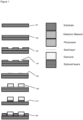
Fig. 1 is a simplified illustration of a process for diamond deposition on a semiconductor, in accordance with an embodiment of the invention. 101 is the semiconductor substrate, 102 after dielectric coating, 103 after dielectric material patterning, 104 after seeding, 105 after photoresist removal, 106 after CVD diamond growth, 107 after dielectric removal, and 108 after semiconductor layers' epitaxial growth. -
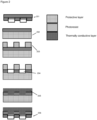
Fig. 2 is a simplified illustration of creating thermally-conductive vias or paths for thermally connecting the diamond covered areas of the device to a heat exchanger, in accordance with an embodiment of the invention. - The present invention provides an approach for producing a semiconductor surface emitting device with highly efficient heat extraction in order to enable high output, high quality power emitting device.
- In order to do so, a diamond layer is grown on a semiconductor substrate. Reference is made to
Figure 1 , which describes a process for doing so, in accordance with an embodiment of the invention. - Starting from a
semiconductor substrate 101, a dielectric material (such as silicon oxide, silicon nitride or any other material suitable for seeding with diamond particles) layer is deposited (102) and then a photoresist (PR) (or any other material that can be patterned by lithography) layer is deposited and patterned by lithography (103), determining areas with PR and areas without PR on the dielectric material surface. Next, a diamond seeding layer, such as diamond slurry, is deposited on the wafer (104). The photoresist is then removed, leaving a patterned diamond seeded surface on the wafer (105). - A diamond layer is deposited, for example by chemical vapor deposition technique (CVD). It should be noted that the diamond will grow preferentially on the regions that have been seeded. Residual growth might occur on the non-seeded regions, however with a very sparse density (islands-like growth), which is easy to remove in the following processes.
- Deposition of diamond is done at high temperature range (>650 0C), which is not applicable on a semiconductor device without protection, as the semiconductor (such as GaAs, InP, GaSb) surface thermally decomposes. Therefore, the dielectric layer has a dual purpose: prevent diamond growth on non-seeded regions on the wafer, and act as nucleation areas for diamond particles in the seeded areas (106).
- Then, using an etching process, the dielectric layer in the non-seeded areas is removed, leaving an intact semiconductor surface. This process finally results in open semiconductor substrate selected areas surrounded by a diamond layer (107). It should be noted that thick diamond layers can be deposited in this way.
- Following this, semiconductor layers are grown, for example using MOCVD (metal organic chemical vapor deposition) or MBE (molecular beam epitaxy) techniques (108). The growth is selective, being effective only in the selected areas where the semiconductor surface is open, free from diamond. The epitaxial layers are grown on the semiconductor surface (e.g. GaAs, InP, GaSb, GaN and alloys of these) and not on the diamond surface. According to the growth conditions, the epitaxial structure might be in contact with the diamond or very close. For thermal conduction, this is less critical than for electric conduction and the diamond layer which will act as a heat spread layer.
- Another issue arises from the fact that the grown diamond layer surface may be hydrogen terminated, as a result of the hydrogen rich growth environment. The hydrogenation of the diamond surface may result in negative electron affinity, pulling the vacuum level below the conduction band minimum (up to -1.3 eV). This can result in charge transfer between the valence band of the diamond and conduction band of the device layer, thus turning the diamond into a P-type semiconductor and injecting unwanted electrons into the device layers. Possible methods to prevent this charge transfer include:
- 1. Surface oxidation, which will result in a diamond surface with a positive electron affinity of 1.7 eV, as shown by Ristein (J., Surface science of diamond: Familiar and amazing. Surface Science, 2006. 600(18): p. 3677-3689).
- 2. Deposition of a thin insulating layer with large band gap and sufficiently small electron affinity, such as SiO2.
- This technique enables a near-contact to full contact of the semiconductor side walls and the diamond layer which will act as a heat spread layer.
- This technique enables a highly efficient heat extraction needed for high power devices, as heat generated in the active region of the device is very close to the diamond heat sink layer, resulting in a higher heat extraction efficiency compared to other techniques where the heat sink is located at a much higher distance from the active region.
- The diamond layer is then connected to a heat exchanger or a thermoelectric cooler.
- In order to remove heat efficiently, it is preferable to connect the diamond covered areas to a heat exchanger located at close proximity. A convenient way to do so is through vias filled with a thermally conducting material such as copper, indium or diamond.
- The process is illustrated in
Fig. 2 :
After optionally thinning the wafer, starting from the growndevice 201, a protective layer such as photoresist is deposited on the grown side of the wafer in order to protect the structures (202). Then a photoresist layer is deposited on the other side of the wafer and is patterned so as to leave holes that are correspondingly in front of the regions where the diamond has been grown previously (203). The wafer is then etched until the diamond layer is reached (204). The holes (204) are then filled with the thermally conducting material (205). The protective layer can then be removed (206). The wafer can then be cut into individual devices, and each device can be put in thermal contact with a passive or active heat sink. - It should be noted that the thermally conducting material can be a metal, such as copper. In such a case, this layer can be pattern by itself in order to provide electric contact to the devices.
Claims (9)
- A method for selective deposition of diamond on a semiconductor substrate and depositing a semiconductor layer, comprising:depositing a dielectric material layer on a semiconductor substrate;depositing and patterning a photoresist layer on top of said dielectric material layer;depositing a diamond seeding layer on said dielectric material layer;removing said photoresist layer and leaving a patterned diamond seeded surface on said dielectric material layer;depositing a diamond layer on said patterned diamond seeded surface;removing said dielectric material from areas not seeded with said diamond seeding layer, leaving an area on said semiconductor substrate with no said diamond layer; anddepositing a semiconductor layer on said area.
- The method according to claim 1, wherein said semiconductor layer is a III-V semiconductor layer.
- The method according to claim 1, wherein said dielectric material comprises silicon oxide or silicon nitride.
- The method according to claim 1, wherein said seeded surface comprises a diamond slurry.
- The method according to claim 1, wherein said diamond layer is deposited using a chemical vapor deposition technique at a temperature above 650 °C.
- The method according to claim 1, wherein vias are produced in the semiconductor substrate and filled with a thermally conducting material.
- The method according to claim 6, wherein the vias are produced using the following steps:covering a side of the semiconductor substrate that has said diamond layer with a protective layer;depositing a photoresist layer on an opposite side of the semiconductor substrate;patterning said photoresist layer so as to leave holes that are aligned with regions where diamond has been grown previously;etching vias in the semiconductor substrate until the diamond layer is reached;removing the photoresist layer;filling said vias with a thermally conducting material; andremoving the protective layer.
- The method according to claim 7, wherein the thermally conducting material comprises copper.
- The method according to claim 7, wherein the thermally conducting material is patterned in order to provide electrical contacts.
Applications Claiming Priority (2)
| Application Number | Priority Date | Filing Date | Title |
|---|---|---|---|
| US201962953558P | 2019-12-25 | 2019-12-25 | |
| PCT/IB2020/062432 WO2021130716A1 (en) | 2019-12-25 | 2020-12-24 | Cooling of high power devices using selective patterned diamond surface |
Publications (3)
| Publication Number | Publication Date |
|---|---|
| EP4062444A1 EP4062444A1 (en) | 2022-09-28 |
| EP4062444C0 EP4062444C0 (en) | 2023-06-07 |
| EP4062444B1 true EP4062444B1 (en) | 2023-06-07 |
Family
ID=74505293
Family Applications (1)
| Application Number | Title | Priority Date | Filing Date |
|---|---|---|---|
| EP20848968.2A Active EP4062444B1 (en) | 2019-12-25 | 2020-12-24 | Cooling of high power devices using selective patterned diamond surface |
Country Status (3)
| Country | Link |
|---|---|
| US (1) | US20220415671A1 (en) |
| EP (1) | EP4062444B1 (en) |
| WO (1) | WO2021130716A1 (en) |
Family Cites Families (9)
| Publication number | Priority date | Publication date | Assignee | Title |
|---|---|---|---|---|
| US20080061309A1 (en) * | 2006-07-21 | 2008-03-13 | Young Sir Chung | Semiconductor device with under-filled heat extractor |
| WO2009073866A1 (en) * | 2007-12-07 | 2009-06-11 | The Government Of The United States Of America, As Represented By The Secretary Of The Navy | Gate after diamond transistor |
| US9496227B2 (en) * | 2009-07-15 | 2016-11-15 | Qualcomm Incorporated | Semiconductor-on-insulator with back side support layer |
| US9685513B2 (en) * | 2012-10-24 | 2017-06-20 | The United States Of America, As Represented By The Secretary Of The Navy | Semiconductor structure or device integrated with diamond |
| US9698024B2 (en) * | 2012-12-06 | 2017-07-04 | Taiwan Semiconductor Manufacturing Co., Ltd. | Partial SOI on power device for breakdown voltage improvement |
| US8993419B1 (en) * | 2013-10-03 | 2015-03-31 | Applied Materials, Inc. | Trench formation with CD less than 10 NM for replacement Fin growth |
| US9246305B1 (en) * | 2014-03-20 | 2016-01-26 | The United States Of America, As Represented By The Secretary Of The Navy | Light-emitting devices with integrated diamond |
| EP3556454B1 (en) * | 2018-04-16 | 2024-05-29 | IMEC vzw | Formation of diamond membranes |
| US10497817B1 (en) * | 2018-07-09 | 2019-12-03 | Wisconsin Alumni Research Foundation | P-n diodes and p-n-p heterojunction bipolar transistors with diamond collectors and current tunneling layers |
-
2020
- 2020-12-24 US US17/787,596 patent/US20220415671A1/en not_active Abandoned
- 2020-12-24 WO PCT/IB2020/062432 patent/WO2021130716A1/en not_active Ceased
- 2020-12-24 EP EP20848968.2A patent/EP4062444B1/en active Active
Also Published As
| Publication number | Publication date |
|---|---|
| EP4062444C0 (en) | 2023-06-07 |
| WO2021130716A1 (en) | 2021-07-01 |
| US20220415671A1 (en) | 2022-12-29 |
| EP4062444A1 (en) | 2022-09-28 |
Similar Documents
| Publication | Publication Date | Title |
|---|---|---|
| US10454241B2 (en) | VCSEL structure with embedded heat sink | |
| CN113396486B (en) | Indium Phosphide VCSEL with Dielectric DBR | |
| CN101853808B (en) | Method of Forming Circuit Structure | |
| US9099632B2 (en) | Light emitting diode emitter substrate with highly reflective metal bonding | |
| US8956897B2 (en) | Method for producing an optoelectronic component and optoelectronic component | |
| EP1386354B1 (en) | Gallium nitride material based semiconductor devices including thermally conductive regions | |
| JP5243256B2 (en) | Monolithically integrated semiconductor materials and devices | |
| JP4571371B2 (en) | Substrates for semiconductor structures with high thermal conductivity | |
| EP2860753B1 (en) | Vertical structure LEDs | |
| US8674405B1 (en) | Gallium—nitride-on-diamond wafers and devices, and methods of manufacture | |
| US20150243848A1 (en) | Light-emitting devices with through-substrate via connections | |
| JP2007067418A (en) | III-nitride light emitting device having double heterostructure light emitting region | |
| CN111989777A (en) | Method for manufacturing an optoelectronic device with a matrix of diodes | |
| US9224921B2 (en) | Method for forming a buried metal layer structure | |
| KR102071163B1 (en) | Iii-v light emitting device including a light extracting structure | |
| JP2004530289A (en) | Gallium nitride material devices and methods including backside vias | |
| JP2023523546A (en) | Method for removing devices using epitaxial lateral overgrowth technique | |
| US8536594B2 (en) | Solid state lighting devices with reduced dimensions and methods of manufacturing | |
| US20220415671A1 (en) | Cooling of high power devices using selective patterned diamond surface | |
| JP2000261097A (en) | Laser diode and method of making laser diode | |
| US20080157090A1 (en) | Transplanted epitaxial regrowth for fabricating large area substrates for electronic devices | |
| CN116438641B (en) | Light emitting diode with vertical structure, preparation method thereof and LED display panel | |
| TW202437630A (en) | Surface emitting laser, method for fabricating surface emitting laser | |
| CN121751836A (en) | Visible light communication semiconductor device, manufacturing method thereof and epitaxial structure | |
| JP2008288538A (en) | P-type layer for group III nitride light emitting device |
Legal Events
| Date | Code | Title | Description |
|---|---|---|---|
| STAA | Information on the status of an ep patent application or granted ep patent |
Free format text: STATUS: UNKNOWN |
|
| STAA | Information on the status of an ep patent application or granted ep patent |
Free format text: STATUS: THE INTERNATIONAL PUBLICATION HAS BEEN MADE |
|
| PUAI | Public reference made under article 153(3) epc to a published international application that has entered the european phase |
Free format text: ORIGINAL CODE: 0009012 |
|
| STAA | Information on the status of an ep patent application or granted ep patent |
Free format text: STATUS: REQUEST FOR EXAMINATION WAS MADE |
|
| 17P | Request for examination filed |
Effective date: 20220622 |
|
| AK | Designated contracting states |
Kind code of ref document: A1 Designated state(s): AL AT BE BG CH CY CZ DE DK EE ES FI FR GB GR HR HU IE IS IT LI LT LU LV MC MK MT NL NO PL PT RO RS SE SI SK SM TR |
|
| GRAP | Despatch of communication of intention to grant a patent |
Free format text: ORIGINAL CODE: EPIDOSNIGR1 |
|
| STAA | Information on the status of an ep patent application or granted ep patent |
Free format text: STATUS: GRANT OF PATENT IS INTENDED |
|
| DAV | Request for validation of the european patent (deleted) | ||
| DAX | Request for extension of the european patent (deleted) | ||
| INTG | Intention to grant announced |
Effective date: 20221201 |
|
| GRAS | Grant fee paid |
Free format text: ORIGINAL CODE: EPIDOSNIGR3 |
|
| GRAA | (expected) grant |
Free format text: ORIGINAL CODE: 0009210 |
|
| STAA | Information on the status of an ep patent application or granted ep patent |
Free format text: STATUS: THE PATENT HAS BEEN GRANTED |
|
| AK | Designated contracting states |
Kind code of ref document: B1 Designated state(s): AL AT BE BG CH CY CZ DE DK EE ES FI FR GB GR HR HU IE IS IT LI LT LU LV MC MK MT NL NO PL PT RO RS SE SI SK SM TR |
|
| REG | Reference to a national code |
Ref country code: GB Ref legal event code: FG4D |
|
| REG | Reference to a national code |
Ref country code: CH Ref legal event code: EP Ref country code: AT Ref legal event code: REF Ref document number: 1577531 Country of ref document: AT Kind code of ref document: T Effective date: 20230615 Ref country code: DE Ref legal event code: R096 Ref document number: 602020012349 Country of ref document: DE |
|
| U01 | Request for unitary effect filed |
Effective date: 20230613 |
|
| U07 | Unitary effect registered |
Designated state(s): AT BE BG DE DK EE FI FR IT LT LU LV MT NL PT SE SI Effective date: 20230622 |
|
| REG | Reference to a national code |
Ref country code: LT Ref legal event code: MG9D |
|
| PG25 | Lapsed in a contracting state [announced via postgrant information from national office to epo] |
Ref country code: NO Free format text: LAPSE BECAUSE OF FAILURE TO SUBMIT A TRANSLATION OF THE DESCRIPTION OR TO PAY THE FEE WITHIN THE PRESCRIBED TIME-LIMIT Effective date: 20230907 Ref country code: ES Free format text: LAPSE BECAUSE OF FAILURE TO SUBMIT A TRANSLATION OF THE DESCRIPTION OR TO PAY THE FEE WITHIN THE PRESCRIBED TIME-LIMIT Effective date: 20230607 |
|
| PG25 | Lapsed in a contracting state [announced via postgrant information from national office to epo] |
Ref country code: RS Free format text: LAPSE BECAUSE OF FAILURE TO SUBMIT A TRANSLATION OF THE DESCRIPTION OR TO PAY THE FEE WITHIN THE PRESCRIBED TIME-LIMIT Effective date: 20230607 Ref country code: HR Free format text: LAPSE BECAUSE OF FAILURE TO SUBMIT A TRANSLATION OF THE DESCRIPTION OR TO PAY THE FEE WITHIN THE PRESCRIBED TIME-LIMIT Effective date: 20230607 Ref country code: GR Free format text: LAPSE BECAUSE OF FAILURE TO SUBMIT A TRANSLATION OF THE DESCRIPTION OR TO PAY THE FEE WITHIN THE PRESCRIBED TIME-LIMIT Effective date: 20230908 |
|
| PG25 | Lapsed in a contracting state [announced via postgrant information from national office to epo] |
Ref country code: SK Free format text: LAPSE BECAUSE OF FAILURE TO SUBMIT A TRANSLATION OF THE DESCRIPTION OR TO PAY THE FEE WITHIN THE PRESCRIBED TIME-LIMIT Effective date: 20230607 |
|
| U20 | Renewal fee for the european patent with unitary effect paid |
Year of fee payment: 4 Effective date: 20231214 |
|
| PG25 | Lapsed in a contracting state [announced via postgrant information from national office to epo] |
Ref country code: IS Free format text: LAPSE BECAUSE OF FAILURE TO SUBMIT A TRANSLATION OF THE DESCRIPTION OR TO PAY THE FEE WITHIN THE PRESCRIBED TIME-LIMIT Effective date: 20231007 |
|
| PG25 | Lapsed in a contracting state [announced via postgrant information from national office to epo] |
Ref country code: SM Free format text: LAPSE BECAUSE OF FAILURE TO SUBMIT A TRANSLATION OF THE DESCRIPTION OR TO PAY THE FEE WITHIN THE PRESCRIBED TIME-LIMIT Effective date: 20230607 Ref country code: SK Free format text: LAPSE BECAUSE OF FAILURE TO SUBMIT A TRANSLATION OF THE DESCRIPTION OR TO PAY THE FEE WITHIN THE PRESCRIBED TIME-LIMIT Effective date: 20230607 Ref country code: RO Free format text: LAPSE BECAUSE OF FAILURE TO SUBMIT A TRANSLATION OF THE DESCRIPTION OR TO PAY THE FEE WITHIN THE PRESCRIBED TIME-LIMIT Effective date: 20230607 Ref country code: IS Free format text: LAPSE BECAUSE OF FAILURE TO SUBMIT A TRANSLATION OF THE DESCRIPTION OR TO PAY THE FEE WITHIN THE PRESCRIBED TIME-LIMIT Effective date: 20231007 Ref country code: CZ Free format text: LAPSE BECAUSE OF FAILURE TO SUBMIT A TRANSLATION OF THE DESCRIPTION OR TO PAY THE FEE WITHIN THE PRESCRIBED TIME-LIMIT Effective date: 20230607 |
|
| PG25 | Lapsed in a contracting state [announced via postgrant information from national office to epo] |
Ref country code: PL Free format text: LAPSE BECAUSE OF FAILURE TO SUBMIT A TRANSLATION OF THE DESCRIPTION OR TO PAY THE FEE WITHIN THE PRESCRIBED TIME-LIMIT Effective date: 20230607 |
|
| REG | Reference to a national code |
Ref country code: DE Ref legal event code: R097 Ref document number: 602020012349 Country of ref document: DE |
|
| U1N | Appointed representative for the unitary patent procedure changed after the registration of the unitary effect |
Representative=s name: WRIGHT, HOWARD HUGH BURNBY; GB |
|
| PLBE | No opposition filed within time limit |
Free format text: ORIGINAL CODE: 0009261 |
|
| STAA | Information on the status of an ep patent application or granted ep patent |
Free format text: STATUS: NO OPPOSITION FILED WITHIN TIME LIMIT |
|
| 26N | No opposition filed |
Effective date: 20240308 |
|
| REG | Reference to a national code |
Ref country code: CH Ref legal event code: PL |
|
| PG25 | Lapsed in a contracting state [announced via postgrant information from national office to epo] |
Ref country code: MC Free format text: LAPSE BECAUSE OF FAILURE TO SUBMIT A TRANSLATION OF THE DESCRIPTION OR TO PAY THE FEE WITHIN THE PRESCRIBED TIME-LIMIT Effective date: 20230607 |
|
| PG25 | Lapsed in a contracting state [announced via postgrant information from national office to epo] |
Ref country code: MC Free format text: LAPSE BECAUSE OF FAILURE TO SUBMIT A TRANSLATION OF THE DESCRIPTION OR TO PAY THE FEE WITHIN THE PRESCRIBED TIME-LIMIT Effective date: 20230607 |
|
| REG | Reference to a national code |
Ref country code: IE Ref legal event code: MM4A |
|
| PG25 | Lapsed in a contracting state [announced via postgrant information from national office to epo] |
Ref country code: IE Free format text: LAPSE BECAUSE OF NON-PAYMENT OF DUE FEES Effective date: 20231224 |
|
| PG25 | Lapsed in a contracting state [announced via postgrant information from national office to epo] |
Ref country code: CH Free format text: LAPSE BECAUSE OF NON-PAYMENT OF DUE FEES Effective date: 20231231 |
|
| PG25 | Lapsed in a contracting state [announced via postgrant information from national office to epo] |
Ref country code: IE Free format text: LAPSE BECAUSE OF NON-PAYMENT OF DUE FEES Effective date: 20231224 Ref country code: CH Free format text: LAPSE BECAUSE OF NON-PAYMENT OF DUE FEES Effective date: 20231231 |
|
| U20 | Renewal fee for the european patent with unitary effect paid |
Year of fee payment: 5 Effective date: 20241213 |
|
| PG25 | Lapsed in a contracting state [announced via postgrant information from national office to epo] |
Ref country code: CY Free format text: LAPSE BECAUSE OF FAILURE TO SUBMIT A TRANSLATION OF THE DESCRIPTION OR TO PAY THE FEE WITHIN THE PRESCRIBED TIME-LIMIT; INVALID AB INITIO Effective date: 20201224 |
|
| PG25 | Lapsed in a contracting state [announced via postgrant information from national office to epo] |
Ref country code: HU Free format text: LAPSE BECAUSE OF FAILURE TO SUBMIT A TRANSLATION OF THE DESCRIPTION OR TO PAY THE FEE WITHIN THE PRESCRIBED TIME-LIMIT; INVALID AB INITIO Effective date: 20201224 |
|
| GBPC | Gb: european patent ceased through non-payment of renewal fee |
Effective date: 20241224 |
|
| PG25 | Lapsed in a contracting state [announced via postgrant information from national office to epo] |
Ref country code: GB Free format text: LAPSE BECAUSE OF NON-PAYMENT OF DUE FEES Effective date: 20241224 |
|
| PG25 | Lapsed in a contracting state [announced via postgrant information from national office to epo] |
Ref country code: TR Free format text: LAPSE BECAUSE OF FAILURE TO SUBMIT A TRANSLATION OF THE DESCRIPTION OR TO PAY THE FEE WITHIN THE PRESCRIBED TIME-LIMIT Effective date: 20230607 |
|
| U20 | Renewal fee for the european patent with unitary effect paid |
Year of fee payment: 6 Effective date: 20251216 |