EP4060809A1 - Antenna structure and electronic device - Google Patents
Antenna structure and electronic device Download PDFInfo
- Publication number
- EP4060809A1 EP4060809A1 EP21182678.9A EP21182678A EP4060809A1 EP 4060809 A1 EP4060809 A1 EP 4060809A1 EP 21182678 A EP21182678 A EP 21182678A EP 4060809 A1 EP4060809 A1 EP 4060809A1
- Authority
- EP
- European Patent Office
- Prior art keywords
- equal
- radiator
- antenna structure
- less
- antenna
- Prior art date
- Legal status (The legal status is an assumption and is not a legal conclusion. Google has not performed a legal analysis and makes no representation as to the accuracy of the status listed.)
- Granted
Links
Images

Classifications
-
- H—ELECTRICITY
- H01—ELECTRIC ELEMENTS
- H01Q—ANTENNAS, i.e. RADIO AERIALS
- H01Q5/00—Arrangements for simultaneous operation of antennas on two or more different wavebands, e.g. dual-band or multi-band arrangements
- H01Q5/30—Arrangements for providing operation on different wavebands
- H01Q5/307—Individual or coupled radiating elements, each element being fed in an unspecified way
- H01Q5/342—Individual or coupled radiating elements, each element being fed in an unspecified way for different propagation modes
- H01Q5/357—Individual or coupled radiating elements, each element being fed in an unspecified way for different propagation modes using a single feed point
- H01Q5/364—Creating multiple current paths
- H01Q5/371—Branching current paths
-
- H—ELECTRICITY
- H01—ELECTRIC ELEMENTS
- H01Q—ANTENNAS, i.e. RADIO AERIALS
- H01Q1/00—Details of, or arrangements associated with, antennas
- H01Q1/12—Supports; Mounting means
- H01Q1/22—Supports; Mounting means by structural association with other equipment or articles
- H01Q1/24—Supports; Mounting means by structural association with other equipment or articles with receiving set
- H01Q1/241—Supports; Mounting means by structural association with other equipment or articles with receiving set used in mobile communications, e.g. GSM
- H01Q1/242—Supports; Mounting means by structural association with other equipment or articles with receiving set used in mobile communications, e.g. GSM specially adapted for hand-held use
- H01Q1/243—Supports; Mounting means by structural association with other equipment or articles with receiving set used in mobile communications, e.g. GSM specially adapted for hand-held use with built-in antennas
-
- H—ELECTRICITY
- H01—ELECTRIC ELEMENTS
- H01Q—ANTENNAS, i.e. RADIO AERIALS
- H01Q1/00—Details of, or arrangements associated with, antennas
- H01Q1/12—Supports; Mounting means
- H01Q1/22—Supports; Mounting means by structural association with other equipment or articles
- H01Q1/24—Supports; Mounting means by structural association with other equipment or articles with receiving set
- H01Q1/241—Supports; Mounting means by structural association with other equipment or articles with receiving set used in mobile communications, e.g. GSM
- H01Q1/242—Supports; Mounting means by structural association with other equipment or articles with receiving set used in mobile communications, e.g. GSM specially adapted for hand-held use
-
- H—ELECTRICITY
- H01—ELECTRIC ELEMENTS
- H01Q—ANTENNAS, i.e. RADIO AERIALS
- H01Q1/00—Details of, or arrangements associated with, antennas
- H01Q1/36—Structural form of radiating elements, e.g. cone, spiral, umbrella; Particular materials used therewith
-
- H—ELECTRICITY
- H01—ELECTRIC ELEMENTS
- H01Q—ANTENNAS, i.e. RADIO AERIALS
- H01Q1/00—Details of, or arrangements associated with, antennas
- H01Q1/48—Earthing means; Earth screens; Counterpoises
-
- H—ELECTRICITY
- H01—ELECTRIC ELEMENTS
- H01Q—ANTENNAS, i.e. RADIO AERIALS
- H01Q1/00—Details of, or arrangements associated with, antennas
- H01Q1/50—Structural association of antennas with earthing switches, lead-in devices or lightning protectors
-
- H—ELECTRICITY
- H01—ELECTRIC ELEMENTS
- H01Q—ANTENNAS, i.e. RADIO AERIALS
- H01Q13/00—Waveguide horns or mouths; Slot antennas; Leaky-waveguide antennas; Equivalent structures causing radiation along the transmission path of a guided wave
- H01Q13/10—Resonant slot antennas
-
- H—ELECTRICITY
- H01—ELECTRIC ELEMENTS
- H01Q—ANTENNAS, i.e. RADIO AERIALS
- H01Q5/00—Arrangements for simultaneous operation of antennas on two or more different wavebands, e.g. dual-band or multi-band arrangements
- H01Q5/20—Arrangements for simultaneous operation of antennas on two or more different wavebands, e.g. dual-band or multi-band arrangements characterised by the operating wavebands
- H01Q5/28—Arrangements for establishing polarisation or beam width over two or more different wavebands
-
- H—ELECTRICITY
- H01—ELECTRIC ELEMENTS
- H01Q—ANTENNAS, i.e. RADIO AERIALS
- H01Q5/00—Arrangements for simultaneous operation of antennas on two or more different wavebands, e.g. dual-band or multi-band arrangements
- H01Q5/30—Arrangements for providing operation on different wavebands
- H01Q5/307—Individual or coupled radiating elements, each element being fed in an unspecified way
-
- H—ELECTRICITY
- H01—ELECTRIC ELEMENTS
- H01Q—ANTENNAS, i.e. RADIO AERIALS
- H01Q5/00—Arrangements for simultaneous operation of antennas on two or more different wavebands, e.g. dual-band or multi-band arrangements
- H01Q5/30—Arrangements for providing operation on different wavebands
- H01Q5/378—Combination of fed elements with parasitic elements
-
- H—ELECTRICITY
- H01—ELECTRIC ELEMENTS
- H01Q—ANTENNAS, i.e. RADIO AERIALS
- H01Q9/00—Electrically-short antennas having dimensions not more than twice the operating wavelength and consisting of conductive active radiating elements
- H01Q9/04—Resonant antennas
- H01Q9/30—Resonant antennas with feed to end of elongated active element, e.g. unipole
- H01Q9/42—Resonant antennas with feed to end of elongated active element, e.g. unipole with folded element, the folded parts being spaced apart a small fraction of the operating wavelength
-
- H—ELECTRICITY
- H04—ELECTRIC COMMUNICATION TECHNIQUE
- H04M—TELEPHONIC COMMUNICATION
- H04M1/00—Substation equipment, e.g. for use by subscribers
- H04M1/02—Constructional features of telephone sets
- H04M1/0202—Portable telephone sets, e.g. cordless phones, mobile phones or bar type handsets
- H04M1/026—Details of the structure or mounting of specific components
- H04M1/0274—Details of the structure or mounting of specific components for an electrical connector module
Definitions
- the present disclosure relates to the technical field of terminals, and more particularly to an antenna structure and an electronic device using a wireless communication technology.
- mainstream 5G communication frequency bands on the market include the N41 frequency band, N77 frequency band, N78 frequency band and N79 frequency band.
- the N41 frequency band, N78 frequency band and N79 frequency band are mainly used in China, and the N77 frequency band may be used abroad. Consequently, mainstream mobile phones on the market support the N41 frequency band, N78 frequency band and N79 frequency band, but cannot implement 5G communication overseas, which limits the application of electronic devices.
- the present disclosure provides an antenna structure and an electronic device, to solve the shortcomings in the related prior art.
- an antenna structure includes: a feed point; and a metal frame.
- the metal frame includes a body, a radiator and a coupling branch.
- the radiator and the coupling branch are both connected to the body, and enclose, together with the body, a clearance area.
- a first end of the radiator away from the body and an end of the coupling branch away from the body cooperate to form an antenna gap, and the antenna gap is connected to the clearance area.
- the radiator is connected to the feed point.
- the radiator includes a through groove and an opening, the through groove runs through the radiator along a height direction of the radiator, and the opening is connected to the through groove along a thickness direction of the radiator. A junction of the feed point and the radiator and the opening are located at both sides of the through groove.
- the antenna structure further includes: a first medium unit arranged in the antenna gap.
- the antenna structure further includes: a second medium unit arranged in the through groove and the opening.
- a part of the radiator located on a side of the through groove away from the feed point has a length of greater than or equal to 12.5 mm and less than or equal to 13.5 mm.
- a part of the radiator connected to the feed point has a length of greater than or equal to 14 mm and less than or equal to 16 mm, and/or has a thickness of greater than or equal to 2 mm and less than or equal to 3 mm.
- the antenna gap has a length being greater than or equal to 1 mm and less than or equal to 1.8 mm.
- a sum of respective lengths of the radiator, the coupling branch, and the antenna gap is greater than or equal to 17 mm, and less than or equal to 19 mm.
- the coupling branch has a length being greater than or equal to 1.5 mm and less than or equal to 2.5 mm, and/or has a thickness of greater than or equal to 6 mm and less than or equal to 8 mm.
- the opening has a length being greater than or equal to 2 mm and less than or equal to 3 mm.
- an interval between the through groove and the antenna gap has a length being greater than or equal to 2 mm and less than or equal to 3 mm.
- a distance from a second end of the radiator connected with the body to the feed point is greater than or equal to 10.5 mm and less than or equal to 11.5 mm.
- the part of the radiator located on the side of the through groove away from the feed point has a thickness being greater than or equal to 2 mm and less than or equal to 3 mm, and/or has a height being greater than or equal to 2 mm and less than or equal to 3 mm.
- the through groove has a dimension being greater than or equal to 2 mm and less than or equal to 3 mm.
- an electronic device includes: a mainboard; and the antenna structure as described in any of the above embodiments, in which the feed point of the antenna structure is arranged at the mainboard.
- the electronic device further includes a grounding element that connects the mainboard and the body.
- the C-shaped radiator 22 can be constructed by arranging the through groove and the opening in the radiator 22, and the resonances of the antenna structure 200 can be constructed to cover N41 frequency band, N77 frequency band, N78 frequency band and N79 frequency band in 5G frequency bands by using a changed shape of the radiator 22.
- the circuitry of the antenna structure 200 may be simplified, which facilitates miniaturization of the antenna structure 200.
- first may also be referred to as the second information
- second information may also be referred to as the first information.
- the term “if' used here may be interpreted as "when” or “upon” or “in response to determining.”
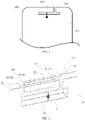
- FIG. 1 is a schematic diagram of an antenna structure 100 in the related art.
- the antenna structure is a three-in-one antenna covering the N41 frequency band, N78 frequency band, and N79 frequency band.
- the antenna structure 100 may include an antenna body 101, an antenna 102 and a coupling unit 103.
- the antenna 102 and the coupling unit 103 are both connected to the antenna body 101.
- the antenna body 101, the antenna 102 and the coupling unit 103 together enclose a clearance area of the antenna structure 100.
- the antenna structure 100 can only cover the N41 frequency band, the N78 frequency band and the N79 frequency band, which limits the application of electronic devices equipped with the antenna structure 100.
- the antenna structure 100 in the related prior art may be equipped with an impedance matching circuit or a tuning switch in an attempt to make the antenna structure 100 cover the N77 frequency band, which leads to a complex circuitry of the antenna structure 100, and causes difficulty in covering the N77 frequency band and N78 frequency band simultaneously in practice due to the limited bandwidth of the antenna 102.
- FIG. 2 is a perspective schematic diagram of an antenna structure according to an exemplary embodiment
- FIG. 3 is a top view of the antenna structure in FIG. 2
- FIG. 4 is a front view of the antenna structure in FIG. 2
- the antenna structure 200 may include a feed point 1 and a metal frame 2
- the metal frame 2 may include a body 21, a radiator 22 and a coupling branch 23
- the radiator 22 and the coupling branch 23 are both connected to the body 21
- the radiator 22, the coupling branch 23 and the body 21 may enclose a clearance area 24.
- the radiator 22 may include a through groove 221 and an opening 222; the through groove 221 may run or extend through the radiator 22 along a height direction (also referred to as a longitudinal direction) of the radiator 22; and the opening 222 may be connected to the through groove 221 along a thickness direction (also referred to as an axial direction) of the radiator 22.
- the feed point 1 is connected to the radiator 22, and a junction where the feed point 1 and the radiator 22 are connected and the opening 222 are located at both sides of the through groove 221, so that a signal fed from the feed point 1 may be transmitted from the junction of the feed point 1 and the radiator 22, around the through groove 221, to a third end 225 of the radiator 22 for forming the opening 222, and the antenna structure 200 can form a C-shaped radiator.
- Various portions of the antenna structure 200 are reasonably dimensioned to allow the antenna structure 200 to completely cover 5G frequency bands.
- the antenna structure 200 may cover the N41 frequency band (2496 MHz to 2690 MHz), the N77 frequency band (3300 MHz to 4200 MHz), the N78 frequency band (3300 MHz to 3800 MHz), and the N79 frequency band (4400 MHz to 5000 MHz).
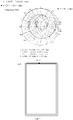
- a graph illustrating antenna performance as shown in FIG. 5 and a Smith chart as shown in FIG. 6 may be obtained by simulation of the antenna structure 200.
- the abscissa of the antenna performance graph represents frequency, and the ordinate represents return loss.
- the antenna structure 200 may be constructed with four resonances to form a broadband antenna, in which a first resonance has a center frequency of2.05 GHZ, a second resonance has a center frequency of 3.07 GHZ, a third resonance has a center frequency of 4.05 GHZ, and a fourth resonance has a center frequency of 4.57 GHZ.
- the center frequency of the third resonance and the center frequency of the fourth resonance are close to the origin, and better impedance matching can be realized for the N77 frequency band and N79 frequency band.
- the C-shaped radiator 22 can be constructed by arranging the through groove and the opening in the radiator 22, and the resonances of the antenna structure 200 can be constructed to cover the N41 frequency band, N77 frequency band, N78 frequency band and N79 frequency band in 5G frequency bands by using a shape change of the radiator 22.
- the circuitry of the antenna structure 200 may be simplified, which facilitates miniaturization of the antenna structure 200.
- lengths and widths of various portions of the antenna structure 200 may be defined.
- a sum of respective lengths of the radiator 22, the antenna gap 25 and the coupling branch 23 is greater than or equal to 17 mm and less than or equal to 19 mm, i.e., 17 mm ⁇ L1 ⁇ 19 mm.
- the present disclosure realizes the miniaturization of the antenna structure 200, improving an internal layout of an electronic device having the antenna structure 200.
- thicknesses and heights of some portions in the antenna structure 200 may also be defined to achieve the optimal resonance frequency.
- the antenna structure 200 may also include a first medium unit 3 and a second medium unit 4.
- the first medium unit 3 may be arranged in the antenna gap 25, and the second medium unit 4 may be arranged in the through groove 221 and the opening 222, to prevent dust from falling into the electronic device configured with the antenna structure 200.
- the above dimensions of the antenna structure 200 may be finely adjusted.
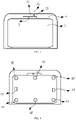
- the present disclosure also provides an electronic device 300 as shown in FIGS. 7 and 8 .
- the electronic device 300 may include a mainboard 5 and the antenna structure 200 as described in any of the above embodiments.
- the feed point 1 of the antenna structure 200 may be arranged at the mainboard 5 and connected to the radiator 22 through a metal strip or other conductive structures.
- the electronic device 300 may also include grounding elements 6 that may connect the metal frame and the mainboard 5 to realize grounding and electromagnetic protection.
- the grounding elements 6 may include grounding screws 6A-6F or metal strips 6G, 6H or other conductive units.
- the electronic device 300 may include a mobile phone terminal or a tablet terminal, which is not limited in the present disclosure.
Landscapes
- Engineering & Computer Science (AREA)
- Computer Networks & Wireless Communication (AREA)
- Signal Processing (AREA)
- Support Of Aerials (AREA)
- Details Of Aerials (AREA)
- Waveguide Aerials (AREA)
Abstract
Description
- The present disclosure relates to the technical field of terminals, and more particularly to an antenna structure and an electronic device using a wireless communication technology.
- At present, for the fifth-generation (5G) mobile communication technology, mainstream 5G communication frequency bands on the market include the N41 frequency band, N77 frequency band, N78 frequency band and N79 frequency band. Among these frequency bands, the N41 frequency band, N78 frequency band and N79 frequency band are mainly used in China, and the N77 frequency band may be used abroad. Consequently, mainstream mobile phones on the market support the N41 frequency band, N78 frequency band and N79 frequency band, but cannot implement 5G communication overseas, which limits the application of electronic devices.
- The present disclosure provides an antenna structure and an electronic device, to solve the shortcomings in the related prior art.
- According to a first aspect of the present disclosure, an antenna structure is provided. The antenna structure includes: a feed point; and a metal frame. The metal frame includes a body, a radiator and a coupling branch. The radiator and the coupling branch are both connected to the body, and enclose, together with the body, a clearance area. A first end of the radiator away from the body and an end of the coupling branch away from the body cooperate to form an antenna gap, and the antenna gap is connected to the clearance area. The radiator is connected to the feed point. The radiator includes a through groove and an opening, the through groove runs through the radiator along a height direction of the radiator, and the opening is connected to the through groove along a thickness direction of the radiator. A junction of the feed point and the radiator and the opening are located at both sides of the through groove.
- Optionally, the antenna structure further includes: a first medium unit arranged in the antenna gap.
- Optionally, the antenna structure further includes: a second medium unit arranged in the through groove and the opening.
- Optionally, a part of the radiator located on a side of the through groove away from the feed point has a length of greater than or equal to 12.5 mm and less than or equal to 13.5 mm.
- Optionally, a part of the radiator connected to the feed point has a length of greater than or equal to 14 mm and less than or equal to 16 mm, and/or has a thickness of greater than or equal to 2 mm and less than or equal to 3 mm.
- Optionally, the antenna gap has a length being greater than or equal to 1 mm and less than or equal to 1.8 mm.
- Optionally, a sum of respective lengths of the radiator, the coupling branch, and the antenna gap is greater than or equal to 17 mm, and less than or equal to 19 mm.
- Optionally, the coupling branch has a length being greater than or equal to 1.5 mm and less than or equal to 2.5 mm, and/or has a thickness of greater than or equal to 6 mm and less than or equal to 8 mm.
- Optionally, the opening has a length being greater than or equal to 2 mm and less than or equal to 3 mm.
- Optionally, an interval between the through groove and the antenna gap has a length being greater than or equal to 2 mm and less than or equal to 3 mm.
- Optionally, a distance from a second end of the radiator connected with the body to the feed point is greater than or equal to 10.5 mm and less than or equal to 11.5 mm.
- Optionally, the part of the radiator located on the side of the through groove away from the feed point has a thickness being greater than or equal to 2 mm and less than or equal to 3 mm, and/or has a height being greater than or equal to 2 mm and less than or equal to 3 mm.
- Optionally, in the thickness direction of the radiator, the through groove has a dimension being greater than or equal to 2 mm and less than or equal to 3 mm.
- According to a second aspect of the present disclosure, an electronic device is provided. The electronic device includes: a mainboard; and the antenna structure as described in any of the above embodiments, in which the feed point of the antenna structure is arranged at the mainboard.
- Optionally, the electronic device further includes a grounding element that connects the mainboard and the body.
- The technical solutions provided by the embodiments of the present disclosure may include the following beneficial effects.
- It can be seen from the above embodiment that in the technical solution of the present disclosure, the C-
shaped radiator 22 can be constructed by arranging the through groove and the opening in theradiator 22, and the resonances of the antenna structure 200 can be constructed to cover N41 frequency band, N77 frequency band, N78 frequency band and N79 frequency band in 5G frequency bands by using a changed shape of theradiator 22. Compared with the scheme in the related prior art that utilizes aperture tuning to realize the frequency band coverage, the circuitry of the antenna structure 200 may be simplified, which facilitates miniaturization of the antenna structure 200. - It should be understood that the above general description and the following detailed description are only exemplary and explanatory and do not limit the present disclosure.
- The accompanying drawings incorporated into the specification and forming part of the specification, illustrate embodiments in accordance with the present disclosure, and are used with the specification to explain the principles of the present disclosure.
-
FIG. 1 is a schematic diagram of an antenna structure in the related art. -
FIG. 2 is a perspective schematic diagram of an antenna structure according to an exemplary embodiment. -
FIG. 3 is a top view of the antenna structure inFIG. 2 . -
FIG. 4 is a front view of the antenna structure inFIG. 2 . -
FIG. 5 is a graph illustrating antenna performance of an antenna structure according to an exemplary embodiment. -
FIG. 6 is a Smith chart of an antenna structure according to an exemplary embodiment. -
FIG. 7 is a schematic diagram of an electronic device according to an exemplary embodiment. -
FIG. 8 is a front view of the electronic device shown inFIG. 7 . -
FIG. 9 is another front view illustrating grounding elements of the electronic device shown inFIG. 7 . - Exemplary embodiments will be described in detail, and examples of the embodiments will be shown in the drawings. When the following description relates to the drawings, the same numbers in different drawings represent the same or similar elements unless otherwise indicated. The implementations described in the following exemplary embodiments do not represent all implementations consistent with the present disclosure. Instead, they are only examples of devices and methods consistent with some aspects of the present disclosure as detailed in the appended claims.
- Terms used in the present disclosure are only for the purpose of describing specific embodiments, and are not intended to limit the present disclosure. As used in the specification and the appended claims, "a/an," "said" and "the" in singular forms are also intended to include plural forms, unless otherwise clearly indicated in the context. It should also be understood that the term "and/or" used herein represents and includes any and all possible combinations of one or more associated listed items.
- It should be understood that although terms such as "first," "second," and "third" may be used to describe various kinds of information in the present disclosure, such information shall not be limited by these terms. These terms are only used to distinguish information of the same type from each other. For example, without departing from the scope of the present disclosure, the first information may also be referred to as the second information, and similarly, the second information may also be referred to as the first information. Depending on the context, the term "if' used here may be interpreted as "when" or "upon" or "in response to determining."
-
FIG. 1 is a schematic diagram of anantenna structure 100 in the related art. The antenna structure is a three-in-one antenna covering the N41 frequency band, N78 frequency band, and N79 frequency band. Theantenna structure 100 may include anantenna body 101, anantenna 102 and acoupling unit 103. Theantenna 102 and thecoupling unit 103 are both connected to theantenna body 101. Theantenna body 101, theantenna 102 and thecoupling unit 103 together enclose a clearance area of theantenna structure 100. However, due to the arrangement of theantenna structure 100 inFIG. 1 , theantenna structure 100 can only cover the N41 frequency band, the N78 frequency band and the N79 frequency band, which limits the application of electronic devices equipped with theantenna structure 100. - In order to broaden the frequency band coverage of the
antenna structure 100, theantenna structure 100 in the related prior art may be equipped with an impedance matching circuit or a tuning switch in an attempt to make theantenna structure 100 cover the N77 frequency band, which leads to a complex circuitry of theantenna structure 100, and causes difficulty in covering the N77 frequency band and N78 frequency band simultaneously in practice due to the limited bandwidth of theantenna 102. - Accordingly, the present disclosure proposes a technical solution to the discussed problem.
FIG. 2 is a perspective schematic diagram of an antenna structure according to an exemplary embodiment;FIG. 3 is a top view of the antenna structure inFIG. 2 ;FIG. 4 is a front view of the antenna structure inFIG. 2 . As shown inFIGS. 2-4 , the antenna structure 200 may include afeed point 1 and ametal frame 2; themetal frame 2 may include abody 21, aradiator 22 and acoupling branch 23; theradiator 22 and thecoupling branch 23 are both connected to thebody 21; and theradiator 22, thecoupling branch 23 and thebody 21 may enclose aclearance area 24. Anantenna gap 25 is formed between afirst end 223 of theradiator 22 directed away from thebody 21 and anend 231 of thecoupling branch 23 directed away from thebody 21, to ensure that the antenna structure 200 may transmit an antenna signal outwards. Theradiator 22 may include a throughgroove 221 and anopening 222; the throughgroove 221 may run or extend through theradiator 22 along a height direction (also referred to as a longitudinal direction) of theradiator 22; and theopening 222 may be connected to the throughgroove 221 along a thickness direction (also referred to as an axial direction) of theradiator 22. Thefeed point 1 is connected to theradiator 22, and a junction where thefeed point 1 and theradiator 22 are connected and theopening 222 are located at both sides of the throughgroove 221, so that a signal fed from thefeed point 1 may be transmitted from the junction of thefeed point 1 and theradiator 22, around the throughgroove 221, to athird end 225 of theradiator 22 for forming theopening 222, and the antenna structure 200 can form a C-shaped radiator. Various portions of the antenna structure 200 are reasonably dimensioned to allow the antenna structure 200 to completely cover 5G frequency bands. Specifically, the antenna structure 200 may cover the N41 frequency band (2496 MHz to 2690 MHz), the N77 frequency band (3300 MHz to 4200 MHz), the N78 frequency band (3300 MHz to 3800 MHz), and the N79 frequency band (4400 MHz to 5000 MHz). - For example, in a case of L1=18mm, L2=15mm, L3=2mm, L4=1.5mm, L5=13mm, L6=2.3mm, L7=2mm, L8=11mm, W1=2mm, W2=2mm, W3=2mm, W4=6mm, W5=2mm, and W6=2mm, a graph illustrating antenna performance as shown in
FIG. 5 and a Smith chart as shown inFIG. 6 may be obtained by simulation of the antenna structure 200. As shown inFIG. 5 andFIG. 6 , the abscissa of the antenna performance graph represents frequency, and the ordinate represents return loss. The resonance of the antenna structure 200 on the left ofFIG. 5 may cover the N41 frequency band, and the resonance of the antenna structure 200 on the right ofFIG. 5 may cover the N77 frequency band, N78 frequency band, and N79 frequency band. As shown inFIG. 6 , with an impedance to be matched of 50 Ohms, the antenna structure 200 may be constructed with four resonances to form a broadband antenna, in which a first resonance has a center frequency of2.05 GHZ, a second resonance has a center frequency of 3.07 GHZ, a third resonance has a center frequency of 4.05 GHZ, and a fourth resonance has a center frequency of 4.57 GHZ. Among them, the center frequency of the third resonance and the center frequency of the fourth resonance are close to the origin, and better impedance matching can be realized for the N77 frequency band and N79 frequency band. - It can be seen from the above embodiment that in the technical solution of the present disclosure, the C-shaped
radiator 22 can be constructed by arranging the through groove and the opening in theradiator 22, and the resonances of the antenna structure 200 can be constructed to cover the N41 frequency band, N77 frequency band, N78 frequency band and N79 frequency band in 5G frequency bands by using a shape change of theradiator 22. Compared with the scheme in the related art that utilizes aperture tuning to realize the frequency band coverage, the circuitry of the antenna structure 200 may be simplified, which facilitates miniaturization of the antenna structure 200. - In order to reach an optimal resonant frequency of the antenna structure 200 and realize the miniaturization of the antenna structure 200 simultaneously, lengths and widths of various portions of the antenna structure 200 may be defined. A sum of respective lengths of the
radiator 22, theantenna gap 25 and thecoupling branch 23 is greater than or equal to 17 mm and less than or equal to 19 mm, i.e., 17 mm≤L1≤19 mm. Compared with the scheme in the related prior art as shown inFIG. 1 , in which theantenna 102 alone has a length of about 25 mm, and theantenna structure 100 has an overall length exceeding 25 mm, the present disclosure realizes the miniaturization of the antenna structure 200, improving an internal layout of an electronic device having the antenna structure 200. - Many ranges of dimensions are contemplated. For example, a part of the radiator 22 connected to the feed point 1 has a length of greater than or equal to 14 mm and less than or equal to 16 mm, i.e., 14 mm≤L2≤6 mm; the coupling branch 23 has a length of greater than or equal to 1.5 mm and less than or equal to 2.5 mm, i.e., 1.5 mm≤L3≤2.5 mm; the antenna gap 25 has a length of greater than or equal to 1 mm and less than or equal to 1.8 mm, i.e., 1 mm≤L4≤1.8 mm, and L1=L2+L3+L4; a part of the radiator 22 located on a side of the through groove 221 away from the feed point 1 has a length of greater than or equal to 12.5 mm and less than or equal to 13.5 mm, i.e., 12.5 mm≤L5≤13.5 mm; the opening 222 may have a length of greater than or equal to 2 mm and less than or equal to 3 mm, i.e., 2 mm ≤L6≤3 mm, and L2=L5+L6; an interval between the through groove 221 and the antenna gap 25 has a length of greater than or equal to 2 mm and less than or equal to 3 mm, i.e., 2 mm ≤L7≤3 mm; a distance from a second end 224 of the radiator 22 connected with the body 21 to the feed point 1 is greater than or equal to 10.5 mm and less than or equal to 11.5 mm, i.e., 10.5 mm≤L8≤11.5 mm.
- Accordingly, thicknesses and heights of some portions in the antenna structure 200 may also be defined to achieve the optimal resonance frequency. For example, the part of the radiator 22 located on the side of the through groove 221 away from the feed point 1 has a thickness of greater than or equal to 2 mm and less than or equal to 3 mm, i.e., 2 mm≤W1≤ 3 mm; in the thickness direction of the radiator 22, the through groove 221 has a dimension of greater than or equal to 2 mm and less than or equal to 3 mm, i.e., 2 mm≤W2≤3 mm; the part of the radiator 22 connected to the feed point 1 has a thickness of greater than or equal to 2 mm and less than or equal to 3 mm, i.e., 2 mm≤W3≤3 mm; the coupling branch 23 has a thickness of greater than or equal to 6 mm and less than or equal to 8 mm, i.e., 6 mm≤W4≤8 mm, and W4=W1+W2+W3; the part of the radiator 22 located on the side of the through groove 221 away from the feed point 1 has a height of greater than or equal to 2 mm and less than or equal to 3 mm, i.e., 2 mm≤W5≤3 mm; the clearance area 24 has a height of greater than or equal to 3 mm and less than or equal to 5 mm, i.e., 3 mm≤W6≤5 mm.
- The antenna structure 200 may also include a first
medium unit 3 and a secondmedium unit 4. The firstmedium unit 3 may be arranged in theantenna gap 25, and the secondmedium unit 4 may be arranged in the throughgroove 221 and theopening 222, to prevent dust from falling into the electronic device configured with the antenna structure 200. According to media conditions of the firstmedium unit 3 and the secondmedium unit 4, the above dimensions of the antenna structure 200 may be finely adjusted. - Based on the antenna structure 200 provided in the present disclosure, the present disclosure also provides an
electronic device 300 as shown inFIGS. 7 and8 . Theelectronic device 300 may include amainboard 5 and the antenna structure 200 as described in any of the above embodiments. Thefeed point 1 of the antenna structure 200 may be arranged at themainboard 5 and connected to theradiator 22 through a metal strip or other conductive structures. As shown inFIG. 9 , theelectronic device 300 may also include groundingelements 6 that may connect the metal frame and themainboard 5 to realize grounding and electromagnetic protection. Thegrounding elements 6 may include groundingscrews 6A-6F ormetal strips electronic device 300 may include a mobile phone terminal or a tablet terminal, which is not limited in the present disclosure. - Other examples of the present disclosure will be apparent to those skilled in the art from consideration of the specification and practice of the present disclosure. The present disclosure is intended to cover any change, use or adaptation of the present disclosure, which complies with the general principles of the present disclosure and includes common knowledge or conventional technical means in the art that are not disclosed herein. The specification and examples are considered to be merely exemplary, and the true scope of the present disclosure are indicated by the following claims.
- It should be understood that the present disclosure is not limited to the specific structures described above and shown in the accompanying drawings, and various modifications and changes may be made without departing from the scope of the present disclosure. The scope of the present disclosure is limited only by the appended claims.
Claims (15)
- An antenna structure (200), comprising:a feed point (1); anda metal frame (2), comprising a body (21), a radiator (22) and a coupling branch (23), wherein the radiator (22) and the coupling branch (23) are both connected to the body (21), and the radiator (22), the coupling branch (23) and the body (21) enclose a clearance area (24), wherein a first end (223) of the radiator (22) away from the body (21) and an end (231) of the coupling branch (23) away from the body (21) cooperate to form an antenna gap (25), and the antenna gap (25) is connected to the clearance area (24), and wherein the radiator (22) is connected to the feed point (1);wherein the radiator (22) comprises a through groove (221) and an opening (222), wherein the through groove (221) runs through the radiator (22) along a height direction of the radiator (22), and the opening (222) is connected to the through groove (221) along a thickness direction of the radiator (22), and wherein a junction of the feed point (1) and the radiator (22) and the opening (222) are located at both sides of the through groove (221).
- The antenna structure (200) according to claim 1, further comprising: a first medium unit (3) arranged in the antenna gap (25).
- The antenna structure (200) according to claim 1 or 2, further comprising: a second medium (4) unit arranged in the through groove (221) and the opening (222).
- The antenna structure (200) according to any one of claims 1 to 3, wherein a part of the radiator (22) located on a side of the through groove (221) away from the feed point (1) has a length of greater than or equal to 12.5 mm and less than or equal to 13.5 mm.
- The antenna structure (200) according to any one of claims 1 to 4, wherein a part of the radiator (22) connected to the feed point (1) has a length of greater than or equal to 14 mm and less than or equal to 16 mm, and/or has a thickness of greater than or equal to 2 mm and less than or equal to 3 mm.
- The antenna structure (200) according to any one of claims 1 to 5, wherein the antenna gap (25) has a length of greater than or equal to 1 mm and less than or equal to 1.8 mm.
- The antenna structure (200) according to any one of claims 1 to 6, wherein a sum of respective lengths of the radiator (22), the coupling branch (23), and the antenna gap (25) is greater than or equal to 17 mm, and less than or equal to 19 mm.
- The antenna structure (200) according to any one of claims 1 to 7, wherein the coupling branch (23) has a length of greater than or equal to 1.5 mm and less than or equal to 2.5 mm, and/or has a thickness of greater than or equal to 6 mm and less than or equal to 8 mm.
- The antenna structure (200) according to any one of claims 1 to 8, wherein the opening (222) has a length of greater than or equal to 2 mm and less than or equal to 3 mm.
- The antenna structure (200) according to any one of claims 1 to 9, wherein an interval between the through groove (221) and the antenna gap (25) has a length of greater than or equal to 2 mm and less than or equal to 3 mm.
- The antenna structure (200) according to any one of claims 1 to 10, wherein a distance from a second end (224) of the radiator (22) connected with the body (21) to the feed point (1) is greater than or equal to 10.5 mm and less than or equal to 11.5 mm.
- The antenna structure (200) according to any one of claims 4 to 11, wherein the part of the radiator (22) located on the side of the through groove (221) away from the feed point (1) has a thickness of greater than or equal to 2 mm and less than or equal to 3 mm, and/or has a height of greater than or equal to 2 mm and less than or equal to 3 mm.
- The antenna structure (200) according to any one of claims 1 to 12, wherein in the thickness direction of the radiator (22), the through groove (221) has a dimension of greater than or equal to 2 mm and less than or equal to 3 mm.
- An electronic device, comprising:a mainboard (5); andthe antenna structure (200) according to any one of claims 1 to 13, wherein the feed point (1) of the antenna structure (200) is arranged at the mainboard (5).
- The electronic device according to claim 14, further comprising a grounding element (6), wherein the grounding element (6) connects the mainboard (5) and the body (21).
Applications Claiming Priority (1)
| Application Number | Priority Date | Filing Date | Title |
|---|---|---|---|
| CN202110287597.2A CN115117594A (en) | 2021-03-17 | 2021-03-17 | Antenna structure and electronic device |
Publications (2)
| Publication Number | Publication Date |
|---|---|
| EP4060809A1 true EP4060809A1 (en) | 2022-09-21 |
| EP4060809B1 EP4060809B1 (en) | 2025-08-20 |
Family
ID=76730315
Family Applications (1)
| Application Number | Title | Priority Date | Filing Date |
|---|---|---|---|
| EP21182678.9A Active EP4060809B1 (en) | 2021-03-17 | 2021-06-30 | Antenna structure and electronic device |
Country Status (5)
| Country | Link |
|---|---|
| US (1) | US11456533B1 (en) |
| EP (1) | EP4060809B1 (en) |
| JP (1) | JP7121168B1 (en) |
| KR (1) | KR102546104B1 (en) |
| CN (1) | CN115117594A (en) |
Families Citing this family (1)
| Publication number | Priority date | Publication date | Assignee | Title |
|---|---|---|---|---|
| TWI853483B (en) * | 2023-03-08 | 2024-08-21 | 啓碁科技股份有限公司 | Antenna system |
Citations (4)
| Publication number | Priority date | Publication date | Assignee | Title |
|---|---|---|---|---|
| US7602341B2 (en) * | 2007-01-25 | 2009-10-13 | Wistron Neweb Corp. | Multi-band antenna |
| US20140118194A1 (en) * | 2012-11-01 | 2014-05-01 | Nvidia Corporation | Multi-band antenna and an electronic device including the same |
| US20140347227A1 (en) * | 2013-05-24 | 2014-11-27 | Microsoft Corporation | Side face antenna for a computing device case |
| US20190237847A1 (en) * | 2018-01-24 | 2019-08-01 | Compal Electronics, Inc. | Antenna module |
Family Cites Families (13)
| Publication number | Priority date | Publication date | Assignee | Title |
|---|---|---|---|---|
| US8259021B2 (en) * | 2008-12-22 | 2012-09-04 | Industrial Technology Research Institute | Electromagnetic radiation apparatus and method for forming the same |
| US8754817B1 (en) * | 2011-12-07 | 2014-06-17 | Amazon Technologies, Inc. | Multi-mode wideband antenna |
| TW201352079A (en) * | 2012-06-13 | 2013-12-16 | Askey Computer Corp | Circuit board having antenna structure |
| CN105322280B (en) * | 2015-05-28 | 2019-07-26 | 维沃移动通信有限公司 | A kind of antenna and mobile device of mobile device |
| US10511079B2 (en) * | 2017-05-09 | 2019-12-17 | Pegatron Corporation | Electronic device and antenna structure thereof |
| CN107565209B (en) * | 2017-07-31 | 2020-10-16 | 北京小米移动软件有限公司 | Mobile terminal and antenna thereof |
| JP6495985B2 (en) * | 2017-09-05 | 2019-04-03 | 株式会社ヨコオ | In-vehicle antenna device |
| CN208637584U (en) * | 2018-08-24 | 2019-03-22 | Oppo广东移动通信有限公司 | Antenna Components and Electronics |
| CN109119747B (en) * | 2018-08-24 | 2021-06-08 | Oppo广东移动通信有限公司 | Antenna Components and Electronics |
| CN109728415B (en) * | 2018-12-28 | 2023-01-06 | 维沃移动通信有限公司 | A wireless electronic communication device |
| CN109586031B (en) * | 2018-12-28 | 2021-04-27 | 维沃移动通信有限公司 | A wireless electronic communication device |
| CN111029747A (en) * | 2019-12-25 | 2020-04-17 | 惠州Tcl移动通信有限公司 | Electronic device |
| CN111628283B (en) * | 2020-06-10 | 2025-04-01 | 安徽华米信息科技有限公司 | Antenna structure and wearable device |
-
2021
- 2021-03-17 CN CN202110287597.2A patent/CN115117594A/en active Pending
- 2021-06-28 US US17/360,445 patent/US11456533B1/en active Active
- 2021-06-28 KR KR1020210083816A patent/KR102546104B1/en active Active
- 2021-06-30 JP JP2021108713A patent/JP7121168B1/en active Active
- 2021-06-30 EP EP21182678.9A patent/EP4060809B1/en active Active
Patent Citations (4)
| Publication number | Priority date | Publication date | Assignee | Title |
|---|---|---|---|---|
| US7602341B2 (en) * | 2007-01-25 | 2009-10-13 | Wistron Neweb Corp. | Multi-band antenna |
| US20140118194A1 (en) * | 2012-11-01 | 2014-05-01 | Nvidia Corporation | Multi-band antenna and an electronic device including the same |
| US20140347227A1 (en) * | 2013-05-24 | 2014-11-27 | Microsoft Corporation | Side face antenna for a computing device case |
| US20190237847A1 (en) * | 2018-01-24 | 2019-08-01 | Compal Electronics, Inc. | Antenna module |
Also Published As
| Publication number | Publication date |
|---|---|
| US11456533B1 (en) | 2022-09-27 |
| JP2022145403A (en) | 2022-10-04 |
| EP4060809B1 (en) | 2025-08-20 |
| JP7121168B1 (en) | 2022-08-17 |
| KR102546104B1 (en) | 2023-06-21 |
| US20220302590A1 (en) | 2022-09-22 |
| CN115117594A (en) | 2022-09-27 |
| KR20220129983A (en) | 2022-09-26 |
Similar Documents
| Publication | Publication Date | Title |
|---|---|---|
| US6801169B1 (en) | Multi-band printed monopole antenna | |
| US6734826B1 (en) | Multi-band antenna | |
| US20040090378A1 (en) | Multi-band antenna structure | |
| US10236558B2 (en) | LTE full-band cellphone antenna structure | |
| US20230238717A1 (en) | Terminal antenna and terminal electronic device | |
| US10547100B2 (en) | Antenna structure and wireless communication device using same | |
| US10566681B2 (en) | Antenna structure and wireless communication device using same | |
| US10700425B2 (en) | Multi-feed antenna | |
| US10498010B2 (en) | Antenna structure and wireless communication device using same | |
| US7068228B2 (en) | Antenna element and mobile telephone device | |
| CN109904628B (en) | Intelligent terminal antenna array | |
| CN114389020B (en) | Antenna structure | |
| US8373601B2 (en) | Multi-band antenna | |
| US11456533B1 (en) | Antenna structure and electronic device | |
| WO2020103314A1 (en) | 5g broadband mimo antenna system employing coupled loop antenna and mobile terminal | |
| TWI784726B (en) | Hybrid antenna structure | |
| CN118174025A (en) | Antenna assembly and electronic equipment | |
| WO2022262822A1 (en) | External tri-band antenna for unmanned aerial vehicle | |
| CN113851843A (en) | Dual-frequency MIMO antenna assembly and mobile terminal | |
| CN115966883A (en) | Hybrid antenna structure | |
| CN212085224U (en) | Multiband Antennas and Mobile Terminals | |
| CN222562960U (en) | Mobile phone antenna unit and mobile device | |
| CN219350682U (en) | Full-band antenna | |
| TWI731792B (en) | Transmission structure with dual-frequency antenna | |
| US20250286266A1 (en) | Speaker module, antenna module and electronic device |
Legal Events
| Date | Code | Title | Description |
|---|---|---|---|
| PUAI | Public reference made under article 153(3) epc to a published international application that has entered the european phase |
Free format text: ORIGINAL CODE: 0009012 |
|
| STAA | Information on the status of an ep patent application or granted ep patent |
Free format text: STATUS: THE APPLICATION HAS BEEN PUBLISHED |
|
| AK | Designated contracting states |
Kind code of ref document: A1 Designated state(s): AL AT BE BG CH CY CZ DE DK EE ES FI FR GB GR HR HU IE IS IT LI LT LU LV MC MK MT NL NO PL PT RO RS SE SI SK SM TR |
|
| STAA | Information on the status of an ep patent application or granted ep patent |
Free format text: STATUS: REQUEST FOR EXAMINATION WAS MADE |
|
| 17P | Request for examination filed |
Effective date: 20221011 |
|
| RBV | Designated contracting states (corrected) |
Designated state(s): AL AT BE BG CH CY CZ DE DK EE ES FI FR GB GR HR HU IE IS IT LI LT LU LV MC MK MT NL NO PL PT RO RS SE SI SK SM TR |
|
| GRAP | Despatch of communication of intention to grant a patent |
Free format text: ORIGINAL CODE: EPIDOSNIGR1 |
|
| STAA | Information on the status of an ep patent application or granted ep patent |
Free format text: STATUS: GRANT OF PATENT IS INTENDED |
|
| RIC1 | Information provided on ipc code assigned before grant |
Ipc: H01Q 13/10 20060101ALI20250303BHEP Ipc: H01Q 9/42 20060101ALI20250303BHEP Ipc: H01Q 5/378 20150101ALI20250303BHEP Ipc: H01Q 1/24 20060101AFI20250303BHEP |
|
| INTG | Intention to grant announced |
Effective date: 20250312 |
|
| GRAS | Grant fee paid |
Free format text: ORIGINAL CODE: EPIDOSNIGR3 |
|
| GRAA | (expected) grant |
Free format text: ORIGINAL CODE: 0009210 |
|
| STAA | Information on the status of an ep patent application or granted ep patent |
Free format text: STATUS: THE PATENT HAS BEEN GRANTED |
|
| AK | Designated contracting states |
Kind code of ref document: B1 Designated state(s): AL AT BE BG CH CY CZ DE DK EE ES FI FR GB GR HR HU IE IS IT LI LT LU LV MC MK MT NL NO PL PT RO RS SE SI SK SM TR |
|
| REG | Reference to a national code |
Ref country code: GB Ref legal event code: FG4D |
|
| REG | Reference to a national code |
Ref country code: CH Ref legal event code: EP |
|
| REG | Reference to a national code |
Ref country code: IE Ref legal event code: FG4D |
|
| REG | Reference to a national code |
Ref country code: DE Ref legal event code: R096 Ref document number: 602021036490 Country of ref document: DE |
|
| REG | Reference to a national code |
Ref country code: NL Ref legal event code: MP Effective date: 20250820 |
|
| PG25 | Lapsed in a contracting state [announced via postgrant information from national office to epo] |
Ref country code: IS Free format text: LAPSE BECAUSE OF FAILURE TO SUBMIT A TRANSLATION OF THE DESCRIPTION OR TO PAY THE FEE WITHIN THE PRESCRIBED TIME-LIMIT Effective date: 20251220 |
|
| PG25 | Lapsed in a contracting state [announced via postgrant information from national office to epo] |
Ref country code: NO Free format text: LAPSE BECAUSE OF FAILURE TO SUBMIT A TRANSLATION OF THE DESCRIPTION OR TO PAY THE FEE WITHIN THE PRESCRIBED TIME-LIMIT Effective date: 20251120 |
|
| REG | Reference to a national code |
Ref country code: LT Ref legal event code: MG9D |
|
| PG25 | Lapsed in a contracting state [announced via postgrant information from national office to epo] |
Ref country code: PT Free format text: LAPSE BECAUSE OF FAILURE TO SUBMIT A TRANSLATION OF THE DESCRIPTION OR TO PAY THE FEE WITHIN THE PRESCRIBED TIME-LIMIT Effective date: 20251222 |
|
| PG25 | Lapsed in a contracting state [announced via postgrant information from national office to epo] |
Ref country code: FI Free format text: LAPSE BECAUSE OF FAILURE TO SUBMIT A TRANSLATION OF THE DESCRIPTION OR TO PAY THE FEE WITHIN THE PRESCRIBED TIME-LIMIT Effective date: 20250820 |
|
| PG25 | Lapsed in a contracting state [announced via postgrant information from national office to epo] |
Ref country code: NL Free format text: LAPSE BECAUSE OF FAILURE TO SUBMIT A TRANSLATION OF THE DESCRIPTION OR TO PAY THE FEE WITHIN THE PRESCRIBED TIME-LIMIT Effective date: 20250820 Ref country code: HR Free format text: LAPSE BECAUSE OF FAILURE TO SUBMIT A TRANSLATION OF THE DESCRIPTION OR TO PAY THE FEE WITHIN THE PRESCRIBED TIME-LIMIT Effective date: 20250820 |
|
| PG25 | Lapsed in a contracting state [announced via postgrant information from national office to epo] |
Ref country code: GR Free format text: LAPSE BECAUSE OF FAILURE TO SUBMIT A TRANSLATION OF THE DESCRIPTION OR TO PAY THE FEE WITHIN THE PRESCRIBED TIME-LIMIT Effective date: 20251121 |
|
| PG25 | Lapsed in a contracting state [announced via postgrant information from national office to epo] |
Ref country code: SE Free format text: LAPSE BECAUSE OF FAILURE TO SUBMIT A TRANSLATION OF THE DESCRIPTION OR TO PAY THE FEE WITHIN THE PRESCRIBED TIME-LIMIT Effective date: 20250820 |
|
| PG25 | Lapsed in a contracting state [announced via postgrant information from national office to epo] |
Ref country code: LV Free format text: LAPSE BECAUSE OF FAILURE TO SUBMIT A TRANSLATION OF THE DESCRIPTION OR TO PAY THE FEE WITHIN THE PRESCRIBED TIME-LIMIT Effective date: 20250820 |
|
| PG25 | Lapsed in a contracting state [announced via postgrant information from national office to epo] |
Ref country code: BG Free format text: LAPSE BECAUSE OF FAILURE TO SUBMIT A TRANSLATION OF THE DESCRIPTION OR TO PAY THE FEE WITHIN THE PRESCRIBED TIME-LIMIT Effective date: 20250820 Ref country code: PL Free format text: LAPSE BECAUSE OF FAILURE TO SUBMIT A TRANSLATION OF THE DESCRIPTION OR TO PAY THE FEE WITHIN THE PRESCRIBED TIME-LIMIT Effective date: 20250820 |
|
| PG25 | Lapsed in a contracting state [announced via postgrant information from national office to epo] |
Ref country code: RS Free format text: LAPSE BECAUSE OF FAILURE TO SUBMIT A TRANSLATION OF THE DESCRIPTION OR TO PAY THE FEE WITHIN THE PRESCRIBED TIME-LIMIT Effective date: 20251120 |
|
| PG25 | Lapsed in a contracting state [announced via postgrant information from national office to epo] |
Ref country code: ES Free format text: LAPSE BECAUSE OF FAILURE TO SUBMIT A TRANSLATION OF THE DESCRIPTION OR TO PAY THE FEE WITHIN THE PRESCRIBED TIME-LIMIT Effective date: 20250820 |
|
| REG | Reference to a national code |
Ref country code: AT Ref legal event code: MK05 Ref document number: 1828375 Country of ref document: AT Kind code of ref document: T Effective date: 20250820 |
|
| PG25 | Lapsed in a contracting state [announced via postgrant information from national office to epo] |
Ref country code: SM Free format text: LAPSE BECAUSE OF FAILURE TO SUBMIT A TRANSLATION OF THE DESCRIPTION OR TO PAY THE FEE WITHIN THE PRESCRIBED TIME-LIMIT Effective date: 20250820 |
|
| PG25 | Lapsed in a contracting state [announced via postgrant information from national office to epo] |
Ref country code: DK Free format text: LAPSE BECAUSE OF FAILURE TO SUBMIT A TRANSLATION OF THE DESCRIPTION OR TO PAY THE FEE WITHIN THE PRESCRIBED TIME-LIMIT Effective date: 20250820 |
|
| PG25 | Lapsed in a contracting state [announced via postgrant information from national office to epo] |
Ref country code: AT Free format text: LAPSE BECAUSE OF FAILURE TO SUBMIT A TRANSLATION OF THE DESCRIPTION OR TO PAY THE FEE WITHIN THE PRESCRIBED TIME-LIMIT Effective date: 20250820 |
|
| PG25 | Lapsed in a contracting state [announced via postgrant information from national office to epo] |
Ref country code: IT Free format text: LAPSE BECAUSE OF FAILURE TO SUBMIT A TRANSLATION OF THE DESCRIPTION OR TO PAY THE FEE WITHIN THE PRESCRIBED TIME-LIMIT Effective date: 20250820 |
|
| PG25 | Lapsed in a contracting state [announced via postgrant information from national office to epo] |
Ref country code: CZ Free format text: LAPSE BECAUSE OF FAILURE TO SUBMIT A TRANSLATION OF THE DESCRIPTION OR TO PAY THE FEE WITHIN THE PRESCRIBED TIME-LIMIT Effective date: 20250820 |
|
| PG25 | Lapsed in a contracting state [announced via postgrant information from national office to epo] |
Ref country code: EE Free format text: LAPSE BECAUSE OF FAILURE TO SUBMIT A TRANSLATION OF THE DESCRIPTION OR TO PAY THE FEE WITHIN THE PRESCRIBED TIME-LIMIT Effective date: 20250820 Ref country code: SK Free format text: LAPSE BECAUSE OF FAILURE TO SUBMIT A TRANSLATION OF THE DESCRIPTION OR TO PAY THE FEE WITHIN THE PRESCRIBED TIME-LIMIT Effective date: 20250820 |