EP4060718A1 - Capacitor structure preparation method, capacitor structure, and memory - Google Patents
Capacitor structure preparation method, capacitor structure, and memory Download PDFInfo
- Publication number
- EP4060718A1 EP4060718A1 EP21783125.4A EP21783125A EP4060718A1 EP 4060718 A1 EP4060718 A1 EP 4060718A1 EP 21783125 A EP21783125 A EP 21783125A EP 4060718 A1 EP4060718 A1 EP 4060718A1
- Authority
- EP
- European Patent Office
- Prior art keywords
- layer
- dielectric constant
- amorphous
- electrode
- capacitor structure
- Prior art date
- Legal status (The legal status is an assumption and is not a legal conclusion. Google has not performed a legal analysis and makes no representation as to the accuracy of the status listed.)
- Granted
Links
Images



Classifications
-
- H—ELECTRICITY
- H10—SEMICONDUCTOR DEVICES; ELECTRIC SOLID-STATE DEVICES NOT OTHERWISE PROVIDED FOR
- H10P—GENERIC PROCESSES OR APPARATUS FOR THE MANUFACTURE OR TREATMENT OF DEVICES COVERED BY CLASS H10
- H10P14/00—Formation of materials, e.g. in the shape of layers or pillars
- H10P14/60—Formation of materials, e.g. in the shape of layers or pillars of insulating materials
- H10P14/65—Formation of materials, e.g. in the shape of layers or pillars of insulating materials characterised by treatments performed before or after the formation of the materials
- H10P14/6516—Formation of materials, e.g. in the shape of layers or pillars of insulating materials characterised by treatments performed before or after the formation of the materials of treatments performed after formation of the materials
- H10P14/6544—Formation of materials, e.g. in the shape of layers or pillars of insulating materials characterised by treatments performed before or after the formation of the materials of treatments performed after formation of the materials to change the morphology of the insulating materials, e.g. transformation of an amorphous layer into a crystalline layer
-
- H—ELECTRICITY
- H10—SEMICONDUCTOR DEVICES; ELECTRIC SOLID-STATE DEVICES NOT OTHERWISE PROVIDED FOR
- H10B—ELECTRONIC MEMORY DEVICES
- H10B12/00—Dynamic random access memory [DRAM] devices
- H10B12/01—Manufacture or treatment
- H10B12/02—Manufacture or treatment for one transistor one-capacitor [1T-1C] memory cells
- H10B12/03—Making the capacitor or connections thereto
-
- H—ELECTRICITY
- H10—SEMICONDUCTOR DEVICES; ELECTRIC SOLID-STATE DEVICES NOT OTHERWISE PROVIDED FOR
- H10B—ELECTRONIC MEMORY DEVICES
- H10B12/00—Dynamic random access memory [DRAM] devices
- H10B12/30—DRAM devices comprising one-transistor - one-capacitor [1T-1C] memory cells
-
- H—ELECTRICITY
- H10—SEMICONDUCTOR DEVICES; ELECTRIC SOLID-STATE DEVICES NOT OTHERWISE PROVIDED FOR
- H10D—INORGANIC ELECTRIC SEMICONDUCTOR DEVICES
- H10D1/00—Resistors, capacitors or inductors
- H10D1/01—Manufacture or treatment
- H10D1/041—Manufacture or treatment of capacitors having no potential barriers
- H10D1/042—Manufacture or treatment of capacitors having no potential barriers using deposition processes to form electrode extensions
-
- H—ELECTRICITY
- H10—SEMICONDUCTOR DEVICES; ELECTRIC SOLID-STATE DEVICES NOT OTHERWISE PROVIDED FOR
- H10D—INORGANIC ELECTRIC SEMICONDUCTOR DEVICES
- H10D1/00—Resistors, capacitors or inductors
- H10D1/60—Capacitors
- H10D1/68—Capacitors having no potential barriers
-
- H—ELECTRICITY
- H10—SEMICONDUCTOR DEVICES; ELECTRIC SOLID-STATE DEVICES NOT OTHERWISE PROVIDED FOR
- H10D—INORGANIC ELECTRIC SEMICONDUCTOR DEVICES
- H10D1/00—Resistors, capacitors or inductors
- H10D1/60—Capacitors
- H10D1/68—Capacitors having no potential barriers
- H10D1/692—Electrodes
- H10D1/711—Electrodes having non-planar surfaces, e.g. formed by texturisation
- H10D1/716—Electrodes having non-planar surfaces, e.g. formed by texturisation having vertical extensions
-
- H—ELECTRICITY
- H10—SEMICONDUCTOR DEVICES; ELECTRIC SOLID-STATE DEVICES NOT OTHERWISE PROVIDED FOR
- H10P—GENERIC PROCESSES OR APPARATUS FOR THE MANUFACTURE OR TREATMENT OF DEVICES COVERED BY CLASS H10
- H10P14/00—Formation of materials, e.g. in the shape of layers or pillars
- H10P14/60—Formation of materials, e.g. in the shape of layers or pillars of insulating materials
- H10P14/69—Inorganic materials
- H10P14/692—Inorganic materials composed of oxides, glassy oxides or oxide-based glasses
- H10P14/6921—Inorganic materials composed of oxides, glassy oxides or oxide-based glasses containing silicon
- H10P14/6928—Inorganic materials composed of oxides, glassy oxides or oxide-based glasses containing silicon the material containing silicon and at least one metal element, e.g. metal silicate based insulators or metal silicon oxynitrides
- H10P14/693—Inorganic materials composed of oxides, glassy oxides or oxide-based glasses containing silicon the material containing silicon and at least one metal element, e.g. metal silicate based insulators or metal silicon oxynitrides the material containing hafnium, e.g. HfSiOx or HfSiON
-
- H—ELECTRICITY
- H10—SEMICONDUCTOR DEVICES; ELECTRIC SOLID-STATE DEVICES NOT OTHERWISE PROVIDED FOR
- H10P—GENERIC PROCESSES OR APPARATUS FOR THE MANUFACTURE OR TREATMENT OF DEVICES COVERED BY CLASS H10
- H10P14/00—Formation of materials, e.g. in the shape of layers or pillars
- H10P14/60—Formation of materials, e.g. in the shape of layers or pillars of insulating materials
- H10P14/69—Inorganic materials
- H10P14/692—Inorganic materials composed of oxides, glassy oxides or oxide-based glasses
- H10P14/6921—Inorganic materials composed of oxides, glassy oxides or oxide-based glasses containing silicon
- H10P14/6928—Inorganic materials composed of oxides, glassy oxides or oxide-based glasses containing silicon the material containing silicon and at least one metal element, e.g. metal silicate based insulators or metal silicon oxynitrides
- H10P14/6934—Inorganic materials composed of oxides, glassy oxides or oxide-based glasses containing silicon the material containing silicon and at least one metal element, e.g. metal silicate based insulators or metal silicon oxynitrides the material containing zirconium, e.g. ZrSiOx
-
- H—ELECTRICITY
- H10—SEMICONDUCTOR DEVICES; ELECTRIC SOLID-STATE DEVICES NOT OTHERWISE PROVIDED FOR
- H10P—GENERIC PROCESSES OR APPARATUS FOR THE MANUFACTURE OR TREATMENT OF DEVICES COVERED BY CLASS H10
- H10P14/00—Formation of materials, e.g. in the shape of layers or pillars
- H10P14/60—Formation of materials, e.g. in the shape of layers or pillars of insulating materials
- H10P14/69—Inorganic materials
- H10P14/692—Inorganic materials composed of oxides, glassy oxides or oxide-based glasses
- H10P14/6938—Inorganic materials composed of oxides, glassy oxides or oxide-based glasses the material containing at least one metal element, e.g. metal oxides, metal oxynitrides or metal oxycarbides
- H10P14/6939—Inorganic materials composed of oxides, glassy oxides or oxide-based glasses the material containing at least one metal element, e.g. metal oxides, metal oxynitrides or metal oxycarbides characterised by the metal
- H10P14/69397—Inorganic materials composed of oxides, glassy oxides or oxide-based glasses the material containing at least one metal element, e.g. metal oxides, metal oxynitrides or metal oxycarbides characterised by the metal the material containing two or more metal elements
-
- H—ELECTRICITY
- H10—SEMICONDUCTOR DEVICES; ELECTRIC SOLID-STATE DEVICES NOT OTHERWISE PROVIDED FOR
- H10D—INORGANIC ELECTRIC SEMICONDUCTOR DEVICES
- H10D1/00—Resistors, capacitors or inductors
- H10D1/60—Capacitors
- H10D1/68—Capacitors having no potential barriers
- H10D1/682—Capacitors having no potential barriers having dielectrics comprising perovskite structures
- H10D1/684—Capacitors having no potential barriers having dielectrics comprising perovskite structures the dielectrics comprising multiple layers, e.g. comprising buffer layers, seed layers or gradient layers
Definitions
- the present application relates to the technical field of semiconductor processes, and in particular to a preparation method for a capacitor structure, a capacitor structure, and a memory.
- a Dynamic Random Access Memory is widely used in various electronic devices because of its high density and high read-write speed.
- the DRAM is generally composed of a plurality of storage units, each usually including a transistor and a capacitor structure. Data information is stored in the capacitor structure, and the transistor controls the reading and writing of the data information in the capacitor structure.
- the capacitor structure generally includes two electrodes disposed opposingly, and a dielectric layer located between the two electrodes.
- the material of the dielectric layer is usually hafnium oxide (HfO 2 ), zirconium oxide (ZrO 2 ), or a perovskite structure material such as calcium titanate (CaTiO 3 ) or barium titanate (BaTiO 3 ).
- the material usually has a high dielectric constant, therefore the dielectric layer can have a good insulating property. However, a large leakage current is generated when the above-described material is in contact with a metal electrode.
- the present application provides a preparation method for a capacitor structure, a capacitor structure, and a memory, which are intended to solve the technical problem of large leakage current of the capacitor structure.
- the present application provides a preparation method for a capacitor structure.
- the preparation method include: forming a dielectric layer on a first electrode; wherein, the dielectric layer including a first amorphous layer and a high dielectric constant layer arranged in a stack, the first amorphous layer maintaining an amorphous structure after annealing, and the high dielectric constant layer being formed by crystallizing an initial dielectric constant layer after annealing; and forming a second electrode on the dielectric layer.
- a dielectric layer is first formed on a first electrode.
- the dielectric layer includes a first amorphous layer and a high dielectric constant layer which are stacked.
- the first amorphous layer maintains an amorphous structure after annealing.
- the high dielectric constant layer is formed by crystallizing an initial dielectric constant layer after annealing.
- a second electrode is then formed on the dielectric layer. Since the first amorphous layer maintains an amorphous structure after annealing, electron migration is unlikely to occur in an amorphous structure, therefore the first amorphous layer can inhibit electron transport, the leakage current of the capacitor structure is reduced, and the performance of the capacitor structure is improved.
- the step of forming a dielectric layer on a first electrode include: forming a first amorphous layer on the first electrode; forming an initial dielectric constant layer on the first amorphous layer; annealing the first amorphous layer and the initial dielectric constant layer, wherein, the first amorphous layer maintaining an amorphous structure after annealing, and the initial dielectric constant layer forming a high dielectric constant layer after annealing; and forming a second amorphous layer on the high dielectric constant layer.
- the material of the second amorphous layer may include silicon oxide, aluminum oxide, hafnium silicate with a mass concentration of silicon of 10% - 50%, or aluminum titanate with a mass concentration of aluminum of 10% - 50%, and the second amorphous layer have a thickness of 0.5 nm - 5 nm.
- the step of forming a dielectric layer on a first electrode include: forming a first amorphous layer on the first electrode; forming an initial dielectric constant layer on the first amorphous layer; forming a second amorphous layer on the initial dielectric constant layer; and annealing the first amorphous layer, the initial dielectric constant layer, and the second amorphous layer. Both the first amorphous layer and the second amorphous layer maintain an amorphous structure after annealing, and the initial dielectric constant layer form a high dielectric constant layer after annealing.
- the material of the second amorphous layer may include hafnium silicate with a mass concentration of silicon of 10% - 50% or aluminum titanate with a mass concentration of aluminum of 10% - 50%, and the second amorphous layer have a thickness of 0.5 nm - 5 nm.
- the material of the first amorphous layer may include hafnium silicate or aluminum titanate.
- the mass concentration of silicon in the hafnium silicate may be 10% - 50%
- the mass concentration of aluminum in the aluminum titanate may be 10% - 50%
- the first amorphous layer may have a thickness of 0.5 nm - 5 nm.
- the material of the initial dielectric constant layer may include silicon-doped hafnium oxide, silicon-doped zirconium oxide, or strontium titanate.
- the mass concentration of silicon in the silicon-doped hafnium oxide and the mass concentration of silicon in the silicon-doped zirconium oxide may be less than or equal to 10%.
- the initial dielectric constant layer may have a thickness of 1 - 10 nm.
- an annealing temperature may be 200°C - 600°C, and an annealing time may be 10 s - 600 s.
- the first amorphous layer and the second amorphous layer may have a dielectric constant of 20 - 50, and the high dielectric constant layer may have a dielectric constant of 40 - 300.
- the present application provides a capacitor structure, which includes a first electrode, a dielectric layer, and a second electrode.
- the first electrode and the second electrode may be disposed opposing each other.
- the dielectric layer may be located between the first electrode and the second electrode and is in contact with the first electrode and the second electrode.
- the dielectric layer may include a first amorphous layer, a high dielectric constant layer, and a second amorphous layer.
- the first amorphous layer is in contact with the first electrode.
- the second amorphous layer is in contact with the second electrode.
- the high dielectric constant layer is located between the first amorphous layer and the second amorphous layer and is in contact with the first amorphous layer and the second amorphous layer.
- the first amorphous layer maintains an amorphous structure after annealing.
- the high dielectric constant layer can be formed by crystallizing an initial dielectric constant layer after annealing.
- the capacitor structure provided by the present application includes a first electrode and a second electrode which are disposed opposing each other, and a dielectric layer which is located between the first electrode and the second electrode and is in contact with the first electrode and the second electrode.
- the dielectric layer includes a first amorphous layer in contact with the first electrode, a second amorphous layer in contact with the second electrode, and a high dielectric constant layer located between the first amorphous layer and the second amorphous layer.
- the high dielectric constant layer is in contact with the first amorphous layer and the second amorphous layer.
- the first amorphous layer maintains an amorphous structure after annealing, and electron migration is unlikely to occur in an amorphous structure, thereby the first amorphous layer can inhibit electron transport, the leakage current of the capacitor structure is reduced, and the performance of the capacitor structure is improved.
- the high dielectric constant layer is formed by crystallizing an initial dielectric constant layer after annealing, and has a higher dielectric constant, therefore the dielectric properties of the capacitor structure can be improved.
- the material of the first amorphous layer may include hafnium silicate with a mass concentration of silicon of 10% - 50% or aluminum titanate with a mass concentration of aluminum of 10% - 50%.
- the material of the initial dielectric constant layer may include silicon-doped hafnium oxide, silicon-doped zirconium oxide, or strontium titanate.
- the material of the second amorphous layer may include silicon oxide, aluminum oxide, hafnium silicate with a mass concentration of silicon of 10% - 50%, or aluminum titanate with a mass concentration of aluminum of 10% - 50%.
- the present application provides a memory.
- the memory may include a transistor and the above-described capacitor structure.
- the memory provided by the present application including the above-described capacitor structure, has the advantages of small leakage current and high dielectric constant. Specific effects are as described above, and detailed descriptions are omitted herein.
- a capacitor structure usually includes two electrodes disposed opposing each other, and a dielectric layer located between the two electrodes.
- the material of the dielectric layer is usually hafnium oxide, zirconium oxide, or a perovskite structure material, which usually has a high dielectric constant.
- a large leakage current is generated when the above-described material is in contact with a metal electrode, therefore the leakage current of the capacitor structure is large.
- An embodiment of the present application provides a preparation method for a capacitor structure.
- a dielectric layer with a first amorphous layer is formed, and the first amorphous layer still maintains an amorphous structure after annealing, electron migration is unlikely to occur in the amorphous structure, therefore the first amorphous layer can inhibit electron transport, reduce the leakage current of the capacitor structure, and improve the performance of the capacitor structure.
- FIG. 1 is a flowchart of a preparation method for a capacitor structure according to an example of the present application.
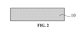
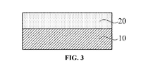
- FIGS. 2 to 6 are schematic structure diagrams of a capacitor structure at various stages of a preparation process. A preparation method for a capacitor structure is described below with reference to FIGS. 1 to 6 .
- the preparation method may include the following steps.
- a dielectric layer is formed on a first electrode.
- the dielectric layer includes a first amorphous layer and a high dielectric constant layer.
- the first amorphous layer maintains an amorphous structure after annealing.
- the high dielectric constant layer is formed by crystallizing an initial dielectric constant layer after annealing.
- the first electrode 10 may be one or more of a metal electrode, a metal oxide electrode, a metal nitride electrode, or a metal silicide electrode.
- the material of the first electrode 10 may be one or more of aluminum (Al), copper (Cu), silver (Ag), gold (Au), molybdenum (Mo), nickel (Ni), cobalt (Co), titanium (Ti), or tungsten (W), or one or more of oxide, nitride, or silicide thereof.
- the first electrode 10 may be formed by a deposition process.
- the first electrode 10 may be formed by a Chemical Vapor Deposition (CVD) process, a Physical Vapor Deposition (PVD) process, or an Atomic Layer Deposition (ALD) process, etc.
- CVD Chemical Vapor Deposition
- PVD Physical Vapor Deposition
- ALD Atomic Layer Deposition
- the embodiment of the present application is, certainly, not limited thereto.
- the first electrode 10 in the embodiment of the present application may be formed by other processes, such as an electroplating process.
- the dielectric layer in the example of the present application may be a multi-layer structure.
- the dielectric layer includes a first amorphous layer 20 and a high dielectric constant layer 30 which are stacked.
- the first amorphous layer 20 may be located on a side of the high dielectric constant layer 30 adjacent to the first electrode 10.
- the first amorphous layer 20 may also be located on a side of the high dielectric constant layer 30 distal from the first electrode 10, and the embodiment of the present application is not limited thereto.
- the material of the first amorphous layer 20 may be an amorphous structure material (amorphous material) and may maintain an amorphous structure after annealing with no or less crystallization. That is, no or less crystalline phase transition occurs in the first amorphous layer 20 at a higher temperature (200°C - 600°C).
- amorphous structure material amorphous material
- a higher temperature 200°C - 600°C.
- the material of the first amorphous layer 20 includes hafnium silicate or aluminum titanate.
- the mass concentration of silicon in the hafnium silicate may be 10% - 50%
- the mass concentration of aluminum in the aluminum titanate may be 10% - 50%.
- the first amorphous layer 20 may have a thickness of 0.5 nm - 5 nm to prevent the first amorphous layer 20 from being too thick and affecting the overall dielectric properties of the capacitor structure.
- the first amorphous layer 20 may have a dielectric constant of 20 - 50.
- the high dielectric constant layer 30 may have a higher dielectric constant, e.g., a value of 40 - 300, to increase the overall dielectric constant of the capacitor structure so that the capacitor structure has better dielectric properties.
- the high dielectric constant layer 30 may be formed by crystallization when the initial dielectric constant layer 31 is annealed, that is, the high dielectric constant layer 30 has a relatively high degree of crystallization.
- the dielectric layer may be formed on the first electrode 10 by using the following steps.
- a first amorphous layer 20 is formed on the first electrode 10.
- a first amorphous layer 20 may be formed on the first electrode 10 by a deposition process, e.g., formed on the first electrode 10 by Plasma Enhanced Chemical Vapor Deposition (PECVD).
- PECVD Plasma Enhanced Chemical Vapor Deposition
- the first amorphous layer 20 can, certainly, also be formed on the first electrode 10 by using a sputtering process, etc., and the embodiment of the present application is not limited thereto.
- an initial dielectric constant layer 31 is formed on the first amorphous layer 20.
- an initial dielectric constant layer 31 is deposited on the first amorphous layer 20.
- the initial dielectric constant layer 31 may have a thickness of 1 - 10 nm.
- the material of the initial dielectric constant layer 31 may be silicon-doped hafnium oxide, silicon-doped zirconium oxide, or strontium titanate (SrTiO 3 ).
- the mass concentration of silicon in the hafnium oxide may be less than or equal to 10%, and the mass concentration of silicon in the zirconium oxide may be less than or equal to 10%.
- the initial dielectric constant layer 31 may undergo a crystalline phase transition at a higher temperature of, e.g., 200°C - 600°C.
- the transition from a low dielectric constant crystalline phase e.g., monoclinic or orthorhombic systems, etc.
- a high dielectric constant crystalline phase e.g., tetragonal or cubic systems, etc.
- the transformed crystalline phase has a higher dielectric constant, and the dielectric constant of the capacitor structure is increased.
- the first amorphous layer 20 and the initial dielectric constant layer 31 are annealed.
- the first amorphous layer 20 maintains an amorphous structure after annealing.
- the initial dielectric constant layer 31 is annealed and crystallized to form a high dielectric constant layer 30 with a higher dielectric constant.
- an annealing temperature may be 200 - 600°C
- an annealing time may be 10 - 600 s.
- the first amorphous layer 20 and the high dielectric constant layer 30 form a dielectric layer.
- step S102 a second electrode is formed on the dielectric layer.
- a second electrode 50 is formed on the dielectric layer.
- the second electrode 50 is deposited and formed on the high dielectric constant layer 30 in the dielectric layer.
- the second electrode 50 may be one or more of a metal electrode, a metal oxide electrode, a metal nitride electrode, or a metal silicide electrode.
- the material and preparation of the second electrode may be referred to the first electrode 10, and detailed descriptions are omitted herein.
- the material of the second electrode 50 and the material of the first electrode 10 may be the same or different.
- the first electrode 10, the first amorphous layer 20, the high dielectric constant layer 30, and the second electrode 50 are sequentially stacked from bottom to top to form the capacitor structure in the example of the present application.
- a dielectric layer is first formed on a first electrode 10.
- the dielectric layer includes a first amorphous layer 20 and a high dielectric constant layer 30 which are stacked.
- the first amorphous layer 20 maintains an amorphous structure after annealing.
- the high dielectric constant layer 30 is formed by annealing and crystallizing an initial dielectric constant layer 31.
- a second electrode 50 is then formed on the dielectric layer. Since the first amorphous layer 20 still has the amorphous structure after annealing, electron migration is unlikely to occur in the amorphous structure, therefore the first amorphous layer 20 can inhibit electron transport, the leakage current of the capacitor structure is reduced, and the performance of the capacitor structure is improved.
- the high dielectric constant layer 30 may have a higher dielectric constant, and the dielectric constant of the capacitor structure can be increased, therefore the capacitor structure has better dielectric properties.
- the dielectric layer can also be formed on the first electrode by using the following steps.
- a first amorphous layer is formed on the first electrode.
- the first amorphous layer may be formed on the first electrode by a deposition process.
- the material of the first amorphous layer may include hafnium silicate with a mass concentration of silicon of 10% - 50% or aluminum titanate having an mass concentration of aluminum of 10% - 50%.
- an initial dielectric constant layer is formed on the first amorphous layer.
- the initial dielectric constant layer is deposited on the first amorphous layer.
- the material of the initial dielectric constant layer may include silicon-doped hafnium oxide, silicon-doped zirconium oxide, or strontium titanate.
- the mass concentration of silicon in the hafnium oxide may be less than or equal to 10%, and the mass concentration of silicon in the zirconium oxide may be less than or equal to 10%.
- the initial dielectric constant layer 31 may have a thickness of 1 - 10 nm.
- the first amorphous layer and the initial dielectric constant layer are annealed.
- the first amorphous layer maintains an amorphous structure after annealing, and the initial dielectric constant layer forms a high dielectric constant layer after annealing. That is, the initial dielectric constant layer 31 is annealed and crystallized to form a high dielectric constant layer 30 having a higher dielectric constant, and the dielectric constant of the capacitor structure is increased.
- the first amorphous layer 20 maintains the amorphous structure after annealing, thereby inhibiting electron transport and reducing the leakage current of the capacitor structure.
- An annealing temperature may be 200 - 600°C, and an annealing time may be 10 - 600 s.
- a second amorphous layer is formed on the high dielectric constant layer.
- the second amorphous layer 40 may have a thickness of 0.5 - 5 nm and a dielectric constant of 20 - 50.
- the material of the second amorphous layer 40 may be an amorphous material.
- the material of the second amorphous layer 40 may include silicon oxide (SiO 2 ) and aluminum oxide (Al 2 O 3 ), and may also include an amorphous material such as hafnium silicate with a mass concentration of silicon of 10% -50% or aluminum titanate with an mass concentration of aluminum of 10% - 50%.
- the second amorphous layer 40 in the example of the present application does not need to be annealed, and therefore it is not limited whether a crystalline phase transition occurs when the second amorphous layer 40 is annealed.
- the first amorphous layer 20, the high dielectric constant layer 30, and the second amorphous layer 40 form the dielectric layer in the example of the present application.
- the dielectric layer may also be formed on the first electrode by using the following steps.
- a first amorphous layer is formed on the first electrode.
- the first amorphous layer may be formed on the first electrode by a deposition process.
- the material of the first amorphous layer may include hafnium silicate with a mass concentration of silicon of 10% - 50% or aluminum titanate with an mass concentration of aluminum of 10% - 50%.
- an initial dielectric constant layer is formed on the first amorphous layer.
- the initial dielectric constant layer may be formed on the first amorphous layer by a deposition process.
- the material of the initial dielectric constant layer may include silicon-doped hafnium oxide, silicon-doped zirconium oxide, or strontium titanate.
- the mass concentration of silicon in the hafnium oxide may be less than or equal to 10%, and the mass concentration of silicon in the zirconium oxide may be less than or equal to 10%.
- the initial dielectric constant layer 31 may have a thickness of 1 - 10 nm.
- a second amorphous layer is formed on the initial dielectric constant layer.
- the second amorphous layer 40 may have a thickness of 0.5 - 5 nm and a dielectric constant of 20 - 50.
- the material of the second amorphous layer 40 may be an amorphous material.
- the material of the second amorphous layer 40 may include an amorphous material with no or less crystallization during annealing such as hafnium silicate having a silicon mass concentration of 10% - 50% or aluminum titanate having an aluminum mass concentration of 10% - 50%.
- an amorphous material with no or less crystallization during annealing such as hafnium silicate having a silicon mass concentration of 10% - 50% or aluminum titanate having an aluminum mass concentration of 10% - 50%.
- the second amorphous layer 40 may maintain the amorphous structure with no or less crystallization during subsequent annealing, so that the second amorphous layer 40 can also inhibit electron transport and further reduce the leakage current of the capacitor structure.
- step S304 the first amorphous layer, the initial dielectric constant layer, and the second amorphous layer are annealed. Both the first amorphous layer and the second amorphous layer maintain an amorphous structure after annealing, and the initial dielectric constant layer forms a high dielectric constant layer after annealing.
- an annealing temperature may be 200 - 600°C
- an annealing time may be 10 - 600 s.
- the initial dielectric constant layer 31 is annealed and crystallized to form a high dielectric constant layer 30 with a relatively high dielectric constant, and the dielectric constant of the capacitor structure is increased.
- the first amorphous layer 20 maintains the amorphous structure after annealing, so that electron transport can be inhibited, and the leakage current of the capacitor structure can be reduced.
- the second amorphous layer 40 maintains the amorphous structure after annealing, so that electron transport can be inhibited, thereby further reducing the leakage current of the capacitor structure.
- the first amorphous layer 20, the high dielectric constant layer 30, and the second amorphous layer 40 form the dielectric layer in the example of the present application.
- the preparation method for the capacitor structure in the example of the present application may be applicable to a columnar capacitor structure.
- the first electrode 10 is roughly U-shaped, and both the inside and the outside of the U-shape are provided with a dielectric layer and a second electrode 50 to form a stacked double-sided columnar capacitor structure.
- the dielectric layer includes a first amorphous layer 20, a high dielectric constant layer 30, and a second amorphous layer 40 in a direction from the first electrode 10 to the second electrode 50.
- the first amorphous layer 20 maintains the amorphous structure after annealing, so as to inhibit electron transport, reduce the leakage current of the capacitor structure, and improve the performance of the capacitor structure.
- the first electrode 10 is formed on a support pad 60.
- the support pad 60 may be formed at the middle and top of a capacitor to ensure that the capacitor is stably supported.
- an example of the present application provides a capacitor structure including a first electrode 10, a dielectric layer, and a second electrode 50.
- the first electrode 10 and the second electrode 50 are disposed opposingly.
- the dielectric layer is disposed between the first electrode 10 and the second electrode 50, and is in contact with the first electrode 10 and the second electrode 50.
- the first electrode 10 and the second electrode 50 may be one or more of a metal electrode, a metal oxide electrode, a metal nitride electrode, or a metal silicide electrode. That is, the capacitor structure in the example of the present application may be a Metal-Insulator-Metal (MIM) capacitor structure, and the example of the present application is, certainly, not limited thereto. For example, the capacitor structure in the example of the present application may also be a Metal-Insulator-Semiconductor (MIS) capacitor, etc.
- MIM Metal-Insulator-Metal
- MIS Metal-Insulator-Semiconductor
- the dielectric layer includes a first amorphous layer 20, a high dielectric constant layer 30, and a second amorphous layer 40.
- the first amorphous layer 20 is in contact with the first electrode 10.
- the second amorphous layer 40 is in contact with the second electrode 50.
- the high dielectric constant layer 30 is located between the first amorphous layer 20 and the second amorphous layer 40 and is in contact with the first amorphous layer 20 and the second amorphous layer 40.
- the first electrode 10, the first amorphous layer 20, the high dielectric constant layer 30, the second amorphous layer 40, and the second electrode 50 are sequentially stacked from bottom to top.
- the first amorphous layer 20 is annealed with no or less crystalline phase transition and may still maintain an amorphous structure. Compared with a crystal structure, electron migration is unlikely to occur in the amorphous structure, so that the first amorphous layer 20 can inhibit electron transport and reduce the leakage current of the capacitor structure.
- the material of the first amorphous layer 20 may be an amorphous structure material such as hafnium silicate or aluminum titanate.
- the concentration of silicon in the hafnium silicate is 10% - 50%
- the concentration of aluminum in the aluminum titanate is 10% - 50%.
- the first amorphous layer may have a dielectric constant of 20 - 50 and a thickness of 0.5 - 5 nm.
- the high dielectric constant layer 30 is formed by annealing and crystallizing an initial dielectric constant layer 31, that is, the crystal phase of the initial dielectric constant layer 31 is changed after annealing from a low dielectric constant crystal phase to a high dielectric constant crystal phase, so that the high dielectric constant layer 30 having a higher dielectric constant is formed, and the dielectric constant of the capacitor structure is increased.
- the high dielectric constant layer 30 may have a dielectric constant of 40 - 300 and a thickness of 1 - 10 nm.
- An annealing temperature may be 200°C - 600°C, and an annealing time may be 10 - 600 s.
- the material of the initial dielectric constant layer 31 may be silicon-doped hafnium oxide, silicon-doped zirconium oxide, or strontium titanate.
- the mass concentration of silicon in the hafnium oxide is less than or equal to 10%, and the mass concentration of silicon in the zirconium oxide is less than or equal to 10%.
- the material of the second amorphous layer 40 may be an amorphous structure material.
- the material of the second amorphous layer 40 may include silicon oxide, aluminum oxide, or an amorphous material such as hafnium silicate or aluminum titanate.
- the concentration of silicon in the hafnium silicate is 10% - 50%
- the concentration of aluminum in the aluminum titanate is 10% - 50%.
- the second amorphous layer may have a dielectric constant of 20 - 50 and a thickness of 0.5 - 5 nm.
- the material of the second amorphous layer 40 may be an amorphous material with no or less crystallization during annealing, such as hafnium silicate or aluminum titanate, so that the annealed second amorphous layer 40 can still maintain an amorphous structure to inhibit electron transport and reduce the leakage current of the capacitor structure.
- the second amorphous layer 40 does not need to be annealed, it is not necessary to limit whether crystallization occurs after the second amorphous layer 40 is annealed, and the material of the second amorphous layer 40 is an amorphous structure material.
- the capacitor structure in the example of the present application may be applicable to a columnar capacitor structure.
- the first electrode 10 is roughly U-shaped, and both the inside and the outside of the U shape are provided with a dielectric layer and a second electrode 50 to form a stacked double-sided columnar capacitor structure.
- the dielectric layer includes a first amorphous layer 20, a high dielectric constant layer 30, and a second amorphous layer 40 in a direction from the first electrode 10 to the second electrode 50.
- the first amorphous layer 20 maintains the amorphous structure after annealing, so as to inhibit electron transport, reduce the leakage current of the capacitor structure, and improve the performance of the capacitor structure.
- the first electrode 10 is formed on a support pad 60.
- the support pad 60 can be formed at the middle and top of a capacitor to ensure that the capacitor is stably supported.
- the capacitor structure in the example of the present application includes a first electrode 10 and a second electrode 50 which are disposed opposing each other, and a dielectric layer which is located between the first electrode 10 and the second electrode 50 and is in contact with the first electrode 10 and the second electrode 50.
- the dielectric layer includes a first amorphous layer 20 in contact with the first electrode 10, a second amorphous layer 40 in contact with the second electrode 50, and a high dielectric constant layer 30 located between the first amorphous layer 20 and the second amorphous layer 40.
- the high dielectric constant layer 30 is in contact with the first amorphous layer 20 and the second amorphous layer 40.
- the first amorphous layer 20 maintains an amorphous structure after annealing, and electron migration is unlikely to occur in the amorphous structure, therefore the leakage current of the capacitor structure is reduced, and the performance of the capacitor structure is improved.
- the high dielectric constant layer 30 is formed by annealing and crystallizing an initial dielectric constant layer 31, and has a higher dielectric constant, therefore the dielectric properties of the capacitor structure can be improved.
- An example of the present application also provides a memory which includes a transistor and a capacitor structure.
- the capacitor structure stores data information, and the transistor controls reading and writing of the data information in the capacitor structure.
- a gate of the transistor is electrically connected to a Word Line (WL) structure of the memory, one of a source and a drain of the transistor is electrically connected to a Bit Line (BL) structure, and the other of the source and the drain is electrically connected to the capacitor structure.
- WL Word Line
- BL Bit Line
- the capacitor structure includes a first electrode, a dielectric layer, and a second electrode.
- the first electrode and the second electrode are disposed opposing each other.
- the dielectric layer is located between the first electrode and the second electrode and is in contact with the first electrode and the second electrode.
- the dielectric layer includes a first amorphous layer, a high dielectric constant layer, and a second amorphous layer which are stacked.
- the first amorphous layer may be located on a side of the dielectric layer adjacent to the first electrode.
- the first electrode and the second electrode may be one or more of a metal electrode, a metal oxide electrode, a metal nitride electrode, or a metal silicide electrode.
- the materials of the first amorphous layer and the second amorphous layer may be an amorphous structure material, which may have a dielectric constant of 20 - 50 and a thickness of 0.5 - 5 nm.
- the first amorphous layer may still maintain an amorphous structure after annealing.
- the high dielectric constant layer may have a dielectric constant of 40 - 300 and a thickness of 1 - 10 nm, and is formed by annealing and crystallizing an initial dielectric constant layer.
- the material of the first amorphous layer includes hafnium silicate with a mass concentration of silicon of 10% - 50% or aluminum titanate having an mass concentration of aluminum of 10% - 50%.
- the material of the initial dielectric constant layer includes silicon-doped hafnium oxide, silicon-doped zirconium oxide, or strontium titanate.
- the material of the second amorphous layer includes silicon oxide, aluminum oxide, hafnium silicate having a mass concentration of silicon of 10% - 50%, or aluminum titanate with a mass concentration of aluminum of 10% - 50%.
- the memory in the example of the present application includes a transistor and a capacitor structure.
- the memory having the capacitor structure in the above-described example, has the advantage of small leakage current. Specific effects are referred to the above-described example, and detailed descriptions are omitted herein.
- orientation or positional relationships indicated by the terms “longitudinal”, “transverse”, “upper”, “lower”, “front”, “rear”, “left”, “right”, “vertical”, “horizontal”, “top”, “bottom”, “inner”, “outer”, etc. are based on the orientation or positional relationships shown in the drawings, which are merely intended to facilitate describing the present application and to simplify the description rather than indicating or implying that the referenced system or element must have a particular orientation and be constructed and operated in a particular orientation. Therefore, the above terms are not to be construed as limiting the present application.
Landscapes
- Engineering & Computer Science (AREA)
- Manufacturing & Machinery (AREA)
- Semiconductor Memories (AREA)
- Chemical & Material Sciences (AREA)
- Crystallography & Structural Chemistry (AREA)
- Semiconductor Integrated Circuits (AREA)
Abstract
Description
- The present application claims priority to
Chinese Patent Application No. 202110075635.8, filed to the China Patent Office on January, 20, 2021 - The present application relates to the technical field of semiconductor processes, and in particular to a preparation method for a capacitor structure, a capacitor structure, and a memory.
- A Dynamic Random Access Memory (DRAM) is widely used in various electronic devices because of its high density and high read-write speed. The DRAM is generally composed of a plurality of storage units, each usually including a transistor and a capacitor structure. Data information is stored in the capacitor structure, and the transistor controls the reading and writing of the data information in the capacitor structure.
- The capacitor structure generally includes two electrodes disposed opposingly, and a dielectric layer located between the two electrodes. The material of the dielectric layer is usually hafnium oxide (HfO2), zirconium oxide (ZrO2), or a perovskite structure material such as calcium titanate (CaTiO3) or barium titanate (BaTiO3). The material usually has a high dielectric constant, therefore the dielectric layer can have a good insulating property. However, a large leakage current is generated when the above-described material is in contact with a metal electrode.
- In view of this, the present application provides a preparation method for a capacitor structure, a capacitor structure, and a memory, which are intended to solve the technical problem of large leakage current of the capacitor structure.
- According to a first aspect, the present application provides a preparation method for a capacitor structure. The preparation method include: forming a dielectric layer on a first electrode; wherein, the dielectric layer including a first amorphous layer and a high dielectric constant layer arranged in a stack, the first amorphous layer maintaining an amorphous structure after annealing, and the high dielectric constant layer being formed by crystallizing an initial dielectric constant layer after annealing; and forming a second electrode on the dielectric layer.
- The preparation method for the capacitor structure provided by the present application has the following advantages:
- In the preparation method for the capacitor structure provided by the present application, a dielectric layer is first formed on a first electrode. The dielectric layer includes a first amorphous layer and a high dielectric constant layer which are stacked. The first amorphous layer maintains an amorphous structure after annealing. The high dielectric constant layer is formed by crystallizing an initial dielectric constant layer after annealing. A second electrode is then formed on the dielectric layer. Since the first amorphous layer maintains an amorphous structure after annealing, electron migration is unlikely to occur in an amorphous structure, therefore the first amorphous layer can inhibit electron transport, the leakage current of the capacitor structure is reduced, and the performance of the capacitor structure is improved.
- In the above-described preparation method for the capacitor structure, the step of forming a dielectric layer on a first electrode include: forming a first amorphous layer on the first electrode; forming an initial dielectric constant layer on the first amorphous layer; annealing the first amorphous layer and the initial dielectric constant layer, wherein, the first amorphous layer maintaining an amorphous structure after annealing, and the initial dielectric constant layer forming a high dielectric constant layer after annealing; and forming a second amorphous layer on the high dielectric constant layer.
- In the above-described preparation method for the capacitor structure, the material of the second amorphous layer may include silicon oxide, aluminum oxide, hafnium silicate with a mass concentration of silicon of 10% - 50%, or aluminum titanate with a mass concentration of aluminum of 10% - 50%, and the second amorphous layer have a thickness of 0.5 nm - 5 nm.
- In the above-described preparation method for the capacitor structure, the step of forming a dielectric layer on a first electrode include: forming a first amorphous layer on the first electrode; forming an initial dielectric constant layer on the first amorphous layer; forming a second amorphous layer on the initial dielectric constant layer; and annealing the first amorphous layer, the initial dielectric constant layer, and the second amorphous layer. Both the first amorphous layer and the second amorphous layer maintain an amorphous structure after annealing, and the initial dielectric constant layer form a high dielectric constant layer after annealing.
- In the above-described preparation method for the capacitor structure, the material of the second amorphous layer may include hafnium silicate with a mass concentration of silicon of 10% - 50% or aluminum titanate with a mass concentration of aluminum of 10% - 50%, and the second amorphous layer have a thickness of 0.5 nm - 5 nm.
- In the above-described preparation method for the capacitor structure, the material of the first amorphous layer may include hafnium silicate or aluminum titanate.
- In the above-described preparation method for the capacitor structure, the mass concentration of silicon in the hafnium silicate may be 10% - 50%, and the mass concentration of aluminum in the aluminum titanate may be 10% - 50%.
- In the above-described preparation method for the capacitor structure, the first amorphous layer may have a thickness of 0.5 nm - 5 nm.
- In the above-described preparation method for the capacitor structure, the material of the initial dielectric constant layer may include silicon-doped hafnium oxide, silicon-doped zirconium oxide, or strontium titanate.
- In the above-described preparation method for the capacitor structure, the mass concentration of silicon in the silicon-doped hafnium oxide and the mass concentration of silicon in the silicon-doped zirconium oxide may be less than or equal to 10%.
- In the above-described preparation method for the capacitor structure, the initial dielectric constant layer may have a thickness of 1 - 10 nm.
- In the above-described preparation method for the capacitor structure, an annealing temperature may be 200°C - 600°C, and an annealing time may be 10 s - 600 s.
- In the above-described preparation method for the capacitor structure, the first amorphous layer and the second amorphous layer may have a dielectric constant of 20 - 50, and the high dielectric constant layer may have a dielectric constant of 40 - 300.
- According to a second aspect, the present application provides a capacitor structure, which includes a first electrode, a dielectric layer, and a second electrode. The first electrode and the second electrode may be disposed opposing each other. The dielectric layer may be located between the first electrode and the second electrode and is in contact with the first electrode and the second electrode. The dielectric layer may include a first amorphous layer, a high dielectric constant layer, and a second amorphous layer. The first amorphous layer is in contact with the first electrode. The second amorphous layer is in contact with the second electrode. The high dielectric constant layer is located between the first amorphous layer and the second amorphous layer and is in contact with the first amorphous layer and the second amorphous layer. The first amorphous layer maintains an amorphous structure after annealing. The high dielectric constant layer can be formed by crystallizing an initial dielectric constant layer after annealing.
- The capacitor structure provided by the present application includes a first electrode and a second electrode which are disposed opposing each other, and a dielectric layer which is located between the first electrode and the second electrode and is in contact with the first electrode and the second electrode. The dielectric layer includes a first amorphous layer in contact with the first electrode, a second amorphous layer in contact with the second electrode, and a high dielectric constant layer located between the first amorphous layer and the second amorphous layer. The high dielectric constant layer is in contact with the first amorphous layer and the second amorphous layer. The first amorphous layer maintains an amorphous structure after annealing, and electron migration is unlikely to occur in an amorphous structure, thereby the first amorphous layer can inhibit electron transport, the leakage current of the capacitor structure is reduced, and the performance of the capacitor structure is improved. In addition, the high dielectric constant layer is formed by crystallizing an initial dielectric constant layer after annealing, and has a higher dielectric constant, therefore the dielectric properties of the capacitor structure can be improved.
- In the above-described capacitor structure, the material of the first amorphous layer may include hafnium silicate with a mass concentration of silicon of 10% - 50% or aluminum titanate with a mass concentration of aluminum of 10% - 50%. The material of the initial dielectric constant layer may include silicon-doped hafnium oxide, silicon-doped zirconium oxide, or strontium titanate. The material of the second amorphous layer may include silicon oxide, aluminum oxide, hafnium silicate with a mass concentration of silicon of 10% - 50%, or aluminum titanate with a mass concentration of aluminum of 10% - 50%.
- According to a third aspect, the present application provides a memory. The memory may include a transistor and the above-described capacitor structure.
- The memory provided by the present application, including the above-described capacitor structure, has the advantages of small leakage current and high dielectric constant. Specific effects are as described above, and detailed descriptions are omitted herein.
- In addition to the above-described technical problems to be solved by the embodiments of the present application, the technical features constituting the technical solutions, and the beneficial effects brought by the technical features of the technical solutions, other technical problems to be solved by the preparation method for the capacitor structure, the capacitor structure, and the memory provided by the embodiments of the present application, other technical features contained in the technical solutions, and the beneficial effects brought by the technical features will be explained in further detail in the detailed description.
-
-
FIG. 1 is a flowchart of a preparation method for a capacitor structure according to an embodiment of the present application. -
FIG. 2 is a schematic structure diagram of a first electrode according to an embodiment of the present application. -
FIG. 3 is a schematic structure diagram after a first amorphous layer is formed according to an embodiment of the present application. -
FIG. 4 is a schematic structure diagram after an initial dielectric constant layer is formed according to an embodiment of the present application. -
FIG. 5 is a schematic structure diagram after a first amorphous layer and an initial dielectric constant layer are annealed according to an embodiment of the present application. -
FIG. 6 is a schematic structure diagram after a second electrode is formed on a high dielectric constant layer according to an embodiment of the present application. -
FIG. 7 is a flowchart of a preparation method for a dielectric layer according to an embodiment of the present application. -
FIG. 8 is a schematic structure diagram after a second amorphous layer is formed on a high dielectric constant layer according to an embodiment of the present application. -
FIG. 9 is a schematic structure diagram after a second electrode is formed on a second amorphous layer according to an embodiment of the present application. -
FIG. 10 is a flowchart of another preparation method for a dielectric layer according to an embodiment of the present application. -
FIG. 11 is a schematic structure diagram after a second amorphous layer is formed on an initial dielectric constant layer according to an embodiment of the present application. -
FIG. 12 is a schematic structure diagram after a first amorphous layer, an initial dielectric constant layer, and a second amorphous layer are annealed according to an embodiment of the present application. -
FIG. 13 is a schematic diagram of a capacitor structure according to an embodiment of the present application. - A capacitor structure usually includes two electrodes disposed opposing each other, and a dielectric layer located between the two electrodes. In a related art, the material of the dielectric layer is usually hafnium oxide, zirconium oxide, or a perovskite structure material, which usually has a high dielectric constant. However, a large leakage current is generated when the above-described material is in contact with a metal electrode, therefore the leakage current of the capacitor structure is large.
- An embodiment of the present application provides a preparation method for a capacitor structure. By forming a dielectric layer with a first amorphous layer is formed, and the first amorphous layer still maintains an amorphous structure after annealing, electron migration is unlikely to occur in the amorphous structure, therefore the first amorphous layer can inhibit electron transport, reduce the leakage current of the capacitor structure, and improve the performance of the capacitor structure.
- To make the objects, technical solutions, and advantages of the embodiments of the present application clearer, the technical solutions in the embodiments of the present application will be clearly and completely described below with reference to the drawings in the embodiments of the present application. It will be apparent that the described embodiments are some, but not all, embodiments of the present application. Based on the embodiments in the present application, all other embodiments obtained by those of ordinary skill in the art without involving any inventive effort are within the scope of protection of the present application.
- Referring to
FIGS. 1 to 6 ,FIG. 1 is a flowchart of a preparation method for a capacitor structure according to an example of the present application.FIGS. 2 to 6 are schematic structure diagrams of a capacitor structure at various stages of a preparation process. A preparation method for a capacitor structure is described below with reference toFIGS. 1 to 6 . The preparation method may include the following steps. - In step S101, a dielectric layer is formed on a first electrode. The dielectric layer includes a first amorphous layer and a high dielectric constant layer. The first amorphous layer maintains an amorphous structure after annealing. The high dielectric constant layer is formed by crystallizing an initial dielectric constant layer after annealing.
- Referring to
FIG. 2 , afirst electrode 10 is provided. Thefirst electrode 10 may be one or more of a metal electrode, a metal oxide electrode, a metal nitride electrode, or a metal silicide electrode. Exemplarily, the material of thefirst electrode 10 may be one or more of aluminum (Al), copper (Cu), silver (Ag), gold (Au), molybdenum (Mo), nickel (Ni), cobalt (Co), titanium (Ti), or tungsten (W), or one or more of oxide, nitride, or silicide thereof. - The
first electrode 10 may be formed by a deposition process. For example, thefirst electrode 10 may be formed by a Chemical Vapor Deposition (CVD) process, a Physical Vapor Deposition (PVD) process, or an Atomic Layer Deposition (ALD) process, etc. The embodiment of the present application is, certainly, not limited thereto. Thefirst electrode 10 in the embodiment of the present application may be formed by other processes, such as an electroplating process. - After the
first electrode 10 is provided, a dielectric layer is formed on thefirst electrode 10. The dielectric layer in the example of the present application may be a multi-layer structure. For example, the dielectric layer includes a firstamorphous layer 20 and a high dielectricconstant layer 30 which are stacked. Exemplarily, the firstamorphous layer 20 may be located on a side of the high dielectricconstant layer 30 adjacent to thefirst electrode 10. The firstamorphous layer 20 may also be located on a side of the high dielectricconstant layer 30 distal from thefirst electrode 10, and the embodiment of the present application is not limited thereto. - The material of the first
amorphous layer 20 may be an amorphous structure material (amorphous material) and may maintain an amorphous structure after annealing with no or less crystallization. That is, no or less crystalline phase transition occurs in the firstamorphous layer 20 at a higher temperature (200°C - 600°C). By such an arrangement, atoms or molecules in the amorphous structure material are in a disordered arrangement state, electrons are unlikely to migrate in the amorphous structure material, therefore electron transport can still be inhibited after the firstamorphous layer 20 is annealed, the leakage current of the capacitor structure is reduced, and the performance of the capacitor structure is improved. - Exemplarily, the material of the first
amorphous layer 20 includes hafnium silicate or aluminum titanate. The mass concentration of silicon in the hafnium silicate may be 10% - 50%, and the mass concentration of aluminum in the aluminum titanate may be 10% - 50%. The firstamorphous layer 20 may have a thickness of 0.5 nm - 5 nm to prevent the firstamorphous layer 20 from being too thick and affecting the overall dielectric properties of the capacitor structure. In the example of the present application, the firstamorphous layer 20 may have a dielectric constant of 20 - 50. - The high dielectric
constant layer 30 may have a higher dielectric constant, e.g., a value of 40 - 300, to increase the overall dielectric constant of the capacitor structure so that the capacitor structure has better dielectric properties. In the example of the present application, the high dielectricconstant layer 30 may be formed by crystallization when the initial dielectricconstant layer 31 is annealed, that is, the high dielectricconstant layer 30 has a relatively high degree of crystallization. - In the example of the present application, the dielectric layer may be formed on the
first electrode 10 by using the following steps. - Firstly, a first
amorphous layer 20 is formed on thefirst electrode 10. Referring toFIG. 3 , a firstamorphous layer 20 may be formed on thefirst electrode 10 by a deposition process, e.g., formed on thefirst electrode 10 by Plasma Enhanced Chemical Vapor Deposition (PECVD). The firstamorphous layer 20 can, certainly, also be formed on thefirst electrode 10 by using a sputtering process, etc., and the embodiment of the present application is not limited thereto. - Secondly, an initial dielectric
constant layer 31 is formed on the firstamorphous layer 20. Referring toFIG. 4 , an initial dielectricconstant layer 31 is deposited on the firstamorphous layer 20. The initial dielectricconstant layer 31 may have a thickness of 1 - 10 nm. - The material of the initial dielectric
constant layer 31 may be silicon-doped hafnium oxide, silicon-doped zirconium oxide, or strontium titanate (SrTiO3). The mass concentration of silicon in the hafnium oxide may be less than or equal to 10%, and the mass concentration of silicon in the zirconium oxide may be less than or equal to 10%. By such an arrangement, the initial dielectricconstant layer 31 may undergo a crystalline phase transition at a higher temperature of, e.g., 200°C - 600°C. Exemplarily, the transition from a low dielectric constant crystalline phase (e.g., monoclinic or orthorhombic systems, etc.) to a high dielectric constant crystalline phase (e.g., tetragonal or cubic systems, etc.), the transformed crystalline phase has a higher dielectric constant, and the dielectric constant of the capacitor structure is increased. - Then, the first
amorphous layer 20 and the initial dielectricconstant layer 31 are annealed. Referring toFIG. 5 , the firstamorphous layer 20 maintains an amorphous structure after annealing. The initial dielectricconstant layer 31 is annealed and crystallized to form a high dielectricconstant layer 30 with a higher dielectric constant. Exemplarily, an annealing temperature may be 200 - 600°C, and an annealing time may be 10 - 600 s. The firstamorphous layer 20 and the high dielectricconstant layer 30 form a dielectric layer. - In step S102, a second electrode is formed on the dielectric layer.
- Referring to
FIG. 6 , asecond electrode 50 is formed on the dielectric layer. Exemplarily, thesecond electrode 50 is deposited and formed on the high dielectricconstant layer 30 in the dielectric layer. Thesecond electrode 50 may be one or more of a metal electrode, a metal oxide electrode, a metal nitride electrode, or a metal silicide electrode. The material and preparation of the second electrode may be referred to thefirst electrode 10, and detailed descriptions are omitted herein. The material of thesecond electrode 50 and the material of thefirst electrode 10 may be the same or different. As shown inFIG. 6 , thefirst electrode 10, the firstamorphous layer 20, the high dielectricconstant layer 30, and thesecond electrode 50 are sequentially stacked from bottom to top to form the capacitor structure in the example of the present application. - In the preparation method for the capacitor structure provided by the example of the present application, a dielectric layer is first formed on a
first electrode 10. The dielectric layer includes a firstamorphous layer 20 and a high dielectricconstant layer 30 which are stacked. The firstamorphous layer 20 maintains an amorphous structure after annealing. The high dielectricconstant layer 30 is formed by annealing and crystallizing an initial dielectricconstant layer 31. Asecond electrode 50 is then formed on the dielectric layer. Since the firstamorphous layer 20 still has the amorphous structure after annealing, electron migration is unlikely to occur in the amorphous structure, therefore the firstamorphous layer 20 can inhibit electron transport, the leakage current of the capacitor structure is reduced, and the performance of the capacitor structure is improved. In addition, the high dielectricconstant layer 30 may have a higher dielectric constant, and the dielectric constant of the capacitor structure can be increased, therefore the capacitor structure has better dielectric properties. - It should be noted that referring to
FIG. 7 , in the example of the present application, the dielectric layer can also be formed on the first electrode by using the following steps. - In step S201, a first amorphous layer is formed on the first electrode. The first amorphous layer may be formed on the first electrode by a deposition process. The material of the first amorphous layer may include hafnium silicate with a mass concentration of silicon of 10% - 50% or aluminum titanate having an mass concentration of aluminum of 10% - 50%.
- In step S202, an initial dielectric constant layer is formed on the first amorphous layer. For example, the initial dielectric constant layer is deposited on the first amorphous layer. The material of the initial dielectric constant layer may include silicon-doped hafnium oxide, silicon-doped zirconium oxide, or strontium titanate. The mass concentration of silicon in the hafnium oxide may be less than or equal to 10%, and the mass concentration of silicon in the zirconium oxide may be less than or equal to 10%. The initial dielectric
constant layer 31 may have a thickness of 1 - 10 nm. - In step S203, the first amorphous layer and the initial dielectric constant layer are annealed. The first amorphous layer maintains an amorphous structure after annealing, and the initial dielectric constant layer forms a high dielectric constant layer after annealing. That is, the initial dielectric
constant layer 31 is annealed and crystallized to form a high dielectricconstant layer 30 having a higher dielectric constant, and the dielectric constant of the capacitor structure is increased. The firstamorphous layer 20 maintains the amorphous structure after annealing, thereby inhibiting electron transport and reducing the leakage current of the capacitor structure. An annealing temperature may be 200 - 600°C, and an annealing time may be 10 - 600 s. - In step S204, a second amorphous layer is formed on the high dielectric constant layer. Referring to
FIG. 8 , the secondamorphous layer 40 may have a thickness of 0.5 - 5 nm and a dielectric constant of 20 - 50. The material of the secondamorphous layer 40 may be an amorphous material. - Exemplarily, the material of the second
amorphous layer 40 may include silicon oxide (SiO2) and aluminum oxide (Al2O3), and may also include an amorphous material such as hafnium silicate with a mass concentration of silicon of 10% -50% or aluminum titanate with an mass concentration of aluminum of 10% - 50%. - The second
amorphous layer 40 in the example of the present application does not need to be annealed, and therefore it is not limited whether a crystalline phase transition occurs when the secondamorphous layer 40 is annealed. The firstamorphous layer 20, the high dielectricconstant layer 30, and the secondamorphous layer 40 form the dielectric layer in the example of the present application. - It should be noted that in the example of the present application, referring to
FIG. 10 , the dielectric layer may also be formed on the first electrode by using the following steps. - In step S301, a first amorphous layer is formed on the first electrode. The first amorphous layer may be formed on the first electrode by a deposition process. The material of the first amorphous layer may include hafnium silicate with a mass concentration of silicon of 10% - 50% or aluminum titanate with an mass concentration of aluminum of 10% - 50%.
- In step S302, an initial dielectric constant layer is formed on the first amorphous layer. For example, the initial dielectric constant layer may be formed on the first amorphous layer by a deposition process. The material of the initial dielectric constant layer may include silicon-doped hafnium oxide, silicon-doped zirconium oxide, or strontium titanate. The mass concentration of silicon in the hafnium oxide may be less than or equal to 10%, and the mass concentration of silicon in the zirconium oxide may be less than or equal to 10%. The initial dielectric
constant layer 31 may have a thickness of 1 - 10 nm. - In step S303, a second amorphous layer is formed on the initial dielectric constant layer. Referring to
FIG. 11 , the secondamorphous layer 40 may have a thickness of 0.5 - 5 nm and a dielectric constant of 20 - 50. The material of the secondamorphous layer 40 may be an amorphous material. - Exemplarily, the material of the second
amorphous layer 40 may include an amorphous material with no or less crystallization during annealing such as hafnium silicate having a silicon mass concentration of 10% - 50% or aluminum titanate having an aluminum mass concentration of 10% - 50%. By such an arrangement, the secondamorphous layer 40 may maintain the amorphous structure with no or less crystallization during subsequent annealing, so that the secondamorphous layer 40 can also inhibit electron transport and further reduce the leakage current of the capacitor structure. - In step S304, the first amorphous layer, the initial dielectric constant layer, and the second amorphous layer are annealed. Both the first amorphous layer and the second amorphous layer maintain an amorphous structure after annealing, and the initial dielectric constant layer forms a high dielectric constant layer after annealing. Exemplarily, an annealing temperature may be 200 - 600°C, and an annealing time may be 10 - 600 s.
- In the present step, referring to
FIG. 12 , the initial dielectricconstant layer 31 is annealed and crystallized to form a high dielectricconstant layer 30 with a relatively high dielectric constant, and the dielectric constant of the capacitor structure is increased. The firstamorphous layer 20 maintains the amorphous structure after annealing, so that electron transport can be inhibited, and the leakage current of the capacitor structure can be reduced. The secondamorphous layer 40 maintains the amorphous structure after annealing, so that electron transport can be inhibited, thereby further reducing the leakage current of the capacitor structure. The firstamorphous layer 20, the high dielectricconstant layer 30, and the secondamorphous layer 40 form the dielectric layer in the example of the present application. - It should be noted that the preparation method for the capacitor structure in the example of the present application may be applicable to a columnar capacitor structure. Exemplarily, in the columnar capacitor structure shown in
FIG. 13 , thefirst electrode 10 is roughly U-shaped, and both the inside and the outside of the U-shape are provided with a dielectric layer and asecond electrode 50 to form a stacked double-sided columnar capacitor structure. - Referring to
FIG. 13 , the dielectric layer includes a firstamorphous layer 20, a high dielectricconstant layer 30, and a secondamorphous layer 40 in a direction from thefirst electrode 10 to thesecond electrode 50. The firstamorphous layer 20 maintains the amorphous structure after annealing, so as to inhibit electron transport, reduce the leakage current of the capacitor structure, and improve the performance of the capacitor structure. In the columnar capacitance structure shown inFIG. 13 , thefirst electrode 10 is formed on asupport pad 60. Thesupport pad 60 may be formed at the middle and top of a capacitor to ensure that the capacitor is stably supported. - Referring to
FIG. 9 , an example of the present application provides a capacitor structure including afirst electrode 10, a dielectric layer, and asecond electrode 50. Thefirst electrode 10 and thesecond electrode 50 are disposed opposingly. The dielectric layer is disposed between thefirst electrode 10 and thesecond electrode 50, and is in contact with thefirst electrode 10 and thesecond electrode 50. - The
first electrode 10 and thesecond electrode 50 may be one or more of a metal electrode, a metal oxide electrode, a metal nitride electrode, or a metal silicide electrode. That is, the capacitor structure in the example of the present application may be a Metal-Insulator-Metal (MIM) capacitor structure, and the example of the present application is, certainly, not limited thereto. For example, the capacitor structure in the example of the present application may also be a Metal-Insulator-Semiconductor (MIS) capacitor, etc. - The dielectric layer includes a first
amorphous layer 20, a high dielectricconstant layer 30, and a secondamorphous layer 40. The firstamorphous layer 20 is in contact with thefirst electrode 10. The secondamorphous layer 40 is in contact with thesecond electrode 50. The high dielectricconstant layer 30 is located between the firstamorphous layer 20 and the secondamorphous layer 40 and is in contact with the firstamorphous layer 20 and the secondamorphous layer 40. Exemplarily, as shown inFIG. 9 , thefirst electrode 10, the firstamorphous layer 20, the high dielectricconstant layer 30, the secondamorphous layer 40, and thesecond electrode 50 are sequentially stacked from bottom to top. - The first
amorphous layer 20 is annealed with no or less crystalline phase transition and may still maintain an amorphous structure. Compared with a crystal structure, electron migration is unlikely to occur in the amorphous structure, so that the firstamorphous layer 20 can inhibit electron transport and reduce the leakage current of the capacitor structure. - The material of the first
amorphous layer 20 may be an amorphous structure material such as hafnium silicate or aluminum titanate. The concentration of silicon in the hafnium silicate is 10% - 50%, and the concentration of aluminum in the aluminum titanate is 10% - 50%. The first amorphous layer may have a dielectric constant of 20 - 50 and a thickness of 0.5 - 5 nm. - The high dielectric
constant layer 30 is formed by annealing and crystallizing an initial dielectricconstant layer 31, that is, the crystal phase of the initial dielectricconstant layer 31 is changed after annealing from a low dielectric constant crystal phase to a high dielectric constant crystal phase, so that the high dielectricconstant layer 30 having a higher dielectric constant is formed, and the dielectric constant of the capacitor structure is increased. The high dielectricconstant layer 30 may have a dielectric constant of 40 - 300 and a thickness of 1 - 10 nm. An annealing temperature may be 200°C - 600°C, and an annealing time may be 10 - 600 s. - The material of the initial dielectric
constant layer 31 may be silicon-doped hafnium oxide, silicon-doped zirconium oxide, or strontium titanate. The mass concentration of silicon in the hafnium oxide is less than or equal to 10%, and the mass concentration of silicon in the zirconium oxide is less than or equal to 10%. - The material of the second
amorphous layer 40 may be an amorphous structure material. Exemplarily, the material of the secondamorphous layer 40 may include silicon oxide, aluminum oxide, or an amorphous material such as hafnium silicate or aluminum titanate. The concentration of silicon in the hafnium silicate is 10% - 50%, and the concentration of aluminum in the aluminum titanate is 10% - 50%. The second amorphous layer may have a dielectric constant of 20 - 50 and a thickness of 0.5 - 5 nm. - It should be noted that when the second
amorphous layer 40 needs to be annealed, the material of the secondamorphous layer 40 may be an amorphous material with no or less crystallization during annealing, such as hafnium silicate or aluminum titanate, so that the annealed secondamorphous layer 40 can still maintain an amorphous structure to inhibit electron transport and reduce the leakage current of the capacitor structure. When the secondamorphous layer 40 does not need to be annealed, it is not necessary to limit whether crystallization occurs after the secondamorphous layer 40 is annealed, and the material of the secondamorphous layer 40 is an amorphous structure material. - It should be noted that the capacitor structure in the example of the present application may be applicable to a columnar capacitor structure. Exemplarily, in the columnar capacitor structure shown in
FIG. 13 , thefirst electrode 10 is roughly U-shaped, and both the inside and the outside of the U shape are provided with a dielectric layer and asecond electrode 50 to form a stacked double-sided columnar capacitor structure. - Referring to
FIG. 13 , the dielectric layer includes a firstamorphous layer 20, a high dielectricconstant layer 30, and a secondamorphous layer 40 in a direction from thefirst electrode 10 to thesecond electrode 50. The firstamorphous layer 20 maintains the amorphous structure after annealing, so as to inhibit electron transport, reduce the leakage current of the capacitor structure, and improve the performance of the capacitor structure. In the columnar capacitance structure shown inFIG. 13 , thefirst electrode 10 is formed on asupport pad 60. Thesupport pad 60 can be formed at the middle and top of a capacitor to ensure that the capacitor is stably supported. - The capacitor structure in the example of the present application includes a
first electrode 10 and asecond electrode 50 which are disposed opposing each other, and a dielectric layer which is located between thefirst electrode 10 and thesecond electrode 50 and is in contact with thefirst electrode 10 and thesecond electrode 50. The dielectric layer includes a firstamorphous layer 20 in contact with thefirst electrode 10, a secondamorphous layer 40 in contact with thesecond electrode 50, and a high dielectricconstant layer 30 located between the firstamorphous layer 20 and the secondamorphous layer 40. The high dielectricconstant layer 30 is in contact with the firstamorphous layer 20 and the secondamorphous layer 40. The firstamorphous layer 20 maintains an amorphous structure after annealing, and electron migration is unlikely to occur in the amorphous structure, therefore the leakage current of the capacitor structure is reduced, and the performance of the capacitor structure is improved. In addition, the high dielectricconstant layer 30 is formed by annealing and crystallizing an initial dielectricconstant layer 31, and has a higher dielectric constant, therefore the dielectric properties of the capacitor structure can be improved. - An example of the present application also provides a memory which includes a transistor and a capacitor structure. The capacitor structure stores data information, and the transistor controls reading and writing of the data information in the capacitor structure. A gate of the transistor is electrically connected to a Word Line (WL) structure of the memory, one of a source and a drain of the transistor is electrically connected to a Bit Line (BL) structure, and the other of the source and the drain is electrically connected to the capacitor structure.
- The capacitor structure includes a first electrode, a dielectric layer, and a second electrode. The first electrode and the second electrode are disposed opposing each other. The dielectric layer is located between the first electrode and the second electrode and is in contact with the first electrode and the second electrode. The dielectric layer includes a first amorphous layer, a high dielectric constant layer, and a second amorphous layer which are stacked. The first amorphous layer may be located on a side of the dielectric layer adjacent to the first electrode.
- The first electrode and the second electrode may be one or more of a metal electrode, a metal oxide electrode, a metal nitride electrode, or a metal silicide electrode. The materials of the first amorphous layer and the second amorphous layer may be an amorphous structure material, which may have a dielectric constant of 20 - 50 and a thickness of 0.5 - 5 nm. The first amorphous layer may still maintain an amorphous structure after annealing. The high dielectric constant layer may have a dielectric constant of 40 - 300 and a thickness of 1 - 10 nm, and is formed by annealing and crystallizing an initial dielectric constant layer.
- Exemplarily, the material of the first amorphous layer includes hafnium silicate with a mass concentration of silicon of 10% - 50% or aluminum titanate having an mass concentration of aluminum of 10% - 50%. The material of the initial dielectric constant layer includes silicon-doped hafnium oxide, silicon-doped zirconium oxide, or strontium titanate. The material of the second amorphous layer includes silicon oxide, aluminum oxide, hafnium silicate having a mass concentration of silicon of 10% - 50%, or aluminum titanate with a mass concentration of aluminum of 10% - 50%.
- The memory in the example of the present application includes a transistor and a capacitor structure. The memory, having the capacitor structure in the above-described example, has the advantage of small leakage current. Specific effects are referred to the above-described example, and detailed descriptions are omitted herein.
- The embodiments or implementations described in this specification are described in an incremental manner, with each embodiment being described with emphasis on differences from the other embodiments, and with reference to like parts throughout the various embodiments.
- Those skilled in the art will appreciate that in the disclosure of the present application, orientation or positional relationships indicated by the terms "longitudinal", "transverse", "upper", "lower", "front", "rear", "left", "right", "vertical", "horizontal", "top", "bottom", "inner", "outer", etc. are based on the orientation or positional relationships shown in the drawings, which are merely intended to facilitate describing the present application and to simplify the description rather than indicating or implying that the referenced system or element must have a particular orientation and be constructed and operated in a particular orientation. Therefore, the above terms are not to be construed as limiting the present application.
- In the descriptions of this specification, the description with reference to the terms "one implementation", "some implementations", "schematic implementations", "example", "specific example", or "some examples", etc. means that particular features, structures, materials, or characteristics described in conjunction with the implementation or example are included in at least one implementation or example of the present application. In this specification, schematic representations of the above terms do not necessarily refer to the same implementation or example. Furthermore, the particular features, structures, materials, or characteristics described may be combined in any suitable manner in any one or more implementations or examples.
- Finally, it should be noted that the above embodiments are merely illustrative of the technical solutions of the present application and are not intended to be limiting thereof. Although the present application has been described in detail with reference to the foregoing embodiments, those of ordinary skill in the art will appreciate that the technical solutions of the foregoing embodiments may still be modified, or some or all of the technical features thereof may be equivalently replaced. These modifications or replacements do not make the essence of the corresponding technical solutions depart from the scope of the technical solutions of the various embodiments of the present application.
Claims (20)
- A preparation method for a capacitor structure, comprising:forming a dielectric layer on a first electrode,wherein the dielectric layer comprises a first amorphous layer and a high dielectric constant layer arranged in a stack, the first amorphous layer maintains an amorphous structure after annealing, and the high dielectric constant layer is formed by crystallizing an initial dielectric constant layer after annealing; andforming a second electrode on the dielectric layer.
- The preparation method for the capacitor structure of claim 1, wherein the step of forming a dielectric layer on a first electrode comprises:forming a first amorphous layer on the first electrode;forming an initial dielectric constant layer on the first amorphous layer;annealing the first amorphous layer and the initial dielectric constant layer, wherein the first amorphous layer maintains an amorphous structure after annealing, and the initial dielectric constant layer forms a high dielectric constant layer after annealing; andforming a second amorphous layer on the high dielectric constant layer.
- The preparation method for the capacitor structure of claim 2, wherein a material of the second amorphous layer comprises silicon oxide, aluminum oxide, hafnium silicate with a mass concentration of silicon of 10-50%, or aluminum titanate with a mass concentration of aluminum of 10-50%, and the second amorphous layer has a thickness of 0.5 - 5 nm.
- The preparation method for the capacitor structure of claim 1, wherein the step of forming a dielectric layer on a first electrode comprises:forming a first amorphous layer on the first electrode;forming an initial dielectric constant layer on the first amorphous layer;forming a second amorphous layer on the initial dielectric constant layer; andannealing the first amorphous layer, the initial dielectric constant layer, and the second amorphous layer, wherein both the first amorphous layer and the second amorphous layer maintain an amorphous structure after annealing, and the initial dielectric constant layer forms a high dielectric constant layer after annealing.
- The preparation method for the capacitor structure of claim 4, wherein a material of the second amorphous layer comprises hafnium silicate having a mass concentration of silicon of 10-50% or aluminum titanate with a mass concentration of aluminum of 10-50%, and the second amorphous layer has a thickness of 0.5 - 5 nm.
- The preparation method for the capacitor structure of claim 1, wherein the material of the first amorphous layer comprises hafnium silicate or aluminum titanate.
- The preparation method for the capacitor structure of claim 6, wherein a mass concentration of silicon in the hafnium silicate is 10% - 50%, and a mass concentration of aluminum in the aluminum titanate is 10% - 50%.
- The preparation method for the capacitor structure of claim 7, wherein the first amorphous layer has a thickness of 0.5 - 5 nm.
- The preparation method for the capacitor structure of claim 1, wherein a material of the initial dielectric constant layer comprises silicon-doped hafnium oxide, silicon-doped zirconium oxide, or strontium titanate.
- The preparation method for the capacitor structure of claim 2, wherein a material of the initial dielectric constant layer comprises silicon-doped hafnium oxide, silicon-doped zirconium oxide, or strontium titanate.
- The preparation method for the capacitor structure of claim 3, wherein a material of the initial dielectric constant layer comprises silicon-doped hafnium oxide, silicon-doped zirconium oxide, or strontium titanate.
- The preparation method for the capacitor structure of claim 4, wherein a material of the initial dielectric constant layer comprises silicon-doped hafnium oxide, silicon-doped zirconium oxide, or strontium titanate.
- The preparation method for the capacitor structure of claim 5, wherein a material of the initial dielectric constant layer comprises silicon-doped hafnium oxide, silicon-doped zirconium oxide, or strontium titanate.
- The preparation method for the capacitor structure of claim 9, wherein both a mass concentration of silicon in the silicon-doped hafnium oxide and a mass concentration of silicon in the silicon-doped zirconium oxide are less than or equal to 10%.
- The preparation method for the capacitor structure of claim 1, wherein the initial dielectric constant layer has a thickness of 1 nm - 10 nm.
- The preparation method for the capacitor structure of claim 1, wherein an annealing temperature is 200°C - 600°C, and an annealing time is 10 s - 600 s.
- The preparation method for the capacitor structure of claim 2, wherein the first amorphous layer and the second amorphous layer have a dielectric constant of 20 - 50, and the high dielectric constant layer has a dielectric constant of 40 - 300.
- A capacitor structure, comprising:a first electrode, a dielectric layer, and a second electrode, whereinthe first electrode and the second electrode are disposed opposing each other, and the dielectric layer is located between the first electrode and the second electrode and is in contact with the first electrode and the second electrode;the dielectric layer comprises a first amorphous layer, a high dielectric constant layer, and a second amorphous layer;the first amorphous layer is in contact with the first electrode, the second amorphous layer is in contact with the second electrode, and the high dielectric constant layer is located between the first amorphous layer and the second amorphous layer and is in contact with the first amorphous layer and the second amorphous layer; andthe first amorphous layer maintains an amorphous structure after annealing, and the high dielectric constant layer is formed by crystallizing an initial dielectric constant layer after annealing.
- The capacitor structure of claim 18, whereina material of the first amorphous layer comprises hafnium silicate with a mass concentration of silicon of 10% - 50% or aluminum titanate with a mass concentration of aluminum of 10% - 50%;a material of the initial dielectric constant layer comprises silicon-doped hafnium oxide, silicon-doped zirconium oxide, or strontium titanate; anda material of the second amorphous layer comprises silicon oxide, aluminum oxide, hafnium silicate with a mass concentration of silicon of 10% - 50%, or aluminum titanate with a mass concentration of aluminum of 10% - 50%.
- A memory device, comprising: a transistor and the capacitor structure of claim 18.
Applications Claiming Priority (2)
| Application Number | Priority Date | Filing Date | Title |
|---|---|---|---|
| CN202110075635.8A CN114864425A (en) | 2021-01-20 | 2021-01-20 | Preparation method of capacitor structure, capacitor structure and memory |
| PCT/CN2021/098877 WO2022156120A1 (en) | 2021-01-20 | 2021-06-08 | Capacitor structure preparation method, capacitor structure, and memory |
Publications (3)
| Publication Number | Publication Date |
|---|---|
| EP4060718A4 EP4060718A4 (en) | 2022-09-21 |
| EP4060718A1 true EP4060718A1 (en) | 2022-09-21 |
| EP4060718B1 EP4060718B1 (en) | 2023-12-06 |
Family
ID=82406553
Family Applications (1)
| Application Number | Title | Priority Date | Filing Date |
|---|---|---|---|
| EP21783125.4A Active EP4060718B1 (en) | 2021-01-20 | 2021-06-08 | Capacitor structure preparation method, capacitor structure, and memory |
Country Status (2)
| Country | Link |
|---|---|
| US (1) | US12469697B2 (en) |
| EP (1) | EP4060718B1 (en) |
Families Citing this family (1)
| Publication number | Priority date | Publication date | Assignee | Title |
|---|---|---|---|---|
| JP2022148213A (en) * | 2021-03-24 | 2022-10-06 | キオクシア株式会社 | semiconductor storage device |
Family Cites Families (10)
| Publication number | Priority date | Publication date | Assignee | Title |
|---|---|---|---|---|
| US7371633B2 (en) | 2001-02-02 | 2008-05-13 | Samsung Electronics Co., Ltd. | Dielectric layer for semiconductor device and method of manufacturing the same |
| US6992344B2 (en) | 2002-12-13 | 2006-01-31 | International Business Machines Corporation | Damascene integration scheme for developing metal-insulator-metal capacitors |
| CN100411116C (en) * | 2003-01-17 | 2008-08-13 | 富士通株式会社 | Method for forming dielectric film |
| JP4722501B2 (en) | 2004-01-29 | 2011-07-13 | 三星電子株式会社 | Multilayer dielectric structure for semiconductor device, semiconductor, and manufacturing method thereof |
| US8323754B2 (en) | 2004-05-21 | 2012-12-04 | Applied Materials, Inc. | Stabilization of high-k dielectric materials |
| US8110469B2 (en) | 2005-08-30 | 2012-02-07 | Micron Technology, Inc. | Graded dielectric layers |
| KR100722989B1 (en) | 2005-11-10 | 2007-05-30 | 주식회사 하이닉스반도체 | Capacitor and manufacturing method thereof |
| JP4353332B2 (en) | 2007-03-14 | 2009-10-28 | エルピーダメモリ株式会社 | Semiconductor device and manufacturing method of semiconductor device |
| KR100967056B1 (en) | 2007-03-29 | 2010-06-29 | 삼성전기주식회사 | Thin Film Capacitors and Printed Circuit Boards with Thin Film Capacitors |
| US7820506B2 (en) * | 2008-10-15 | 2010-10-26 | Micron Technology, Inc. | Capacitors, dielectric structures, and methods of forming dielectric structures |
-
2021
- 2021-06-08 EP EP21783125.4A patent/EP4060718B1/en active Active
- 2021-08-09 US US17/444,690 patent/US12469697B2/en active Active
Also Published As
| Publication number | Publication date |
|---|---|
| US12469697B2 (en) | 2025-11-11 |
| EP4060718A4 (en) | 2022-09-21 |
| EP4060718B1 (en) | 2023-12-06 |
| US20220230876A1 (en) | 2022-07-21 |
Similar Documents
| Publication | Publication Date | Title |
|---|---|---|
| US10748914B2 (en) | Ferroelectric capacitor, ferroelectric field effect transistor, and method used in forming an electronic component comprising conductive material and ferroelectric material | |
| US8541283B2 (en) | High performance dielectric stack for DRAM capacitor | |
| US8574983B2 (en) | Method for fabricating a DRAM capacitor having increased thermal and chemical stability | |
| EP1383162B1 (en) | Deposition method of dielectric layer | |
| US8542523B2 (en) | Method for fabricating a DRAM capacitor having increased thermal and chemical stability | |
| US8679939B2 (en) | Manufacturable high-k DRAM MIM capacitor structure | |
| US8847397B2 (en) | High work function, manufacturable top electrode | |
| US8574998B2 (en) | Leakage reduction in DRAM MIM capacitors | |
| US8722504B2 (en) | Interfacial layer for DRAM capacitor | |
| US8541282B2 (en) | Blocking layers for leakage current reduction in DRAM devices | |
| US8541868B2 (en) | Top electrode templating for DRAM capacitor | |
| CN101542657A (en) | Method of forming a structure having a high dielectric constant and a structure having a high dielectric constant | |
| US8652927B2 (en) | Integration of non-noble DRAM electrode | |
| US8569819B1 (en) | Doped electrodes for DRAM applications | |
| WO2023216965A1 (en) | Ferroelectric memory and forming method therefor, and electronic device | |
| WO2012021318A2 (en) | A high-k dielectric material and methods of forming the high-k dielectric material | |
| EP4060718B1 (en) | Capacitor structure preparation method, capacitor structure, and memory | |
| US12127415B2 (en) | Manufacturing method for capacitor structure, capacitor structure and memory | |
| US8647960B2 (en) | Anneal to minimize leakage current in DRAM capacitor | |
| US8853049B2 (en) | Single-sided non-noble metal electrode hybrid MIM stack for DRAM devices | |
| WO2022156120A1 (en) | Capacitor structure preparation method, capacitor structure, and memory |
Legal Events
| Date | Code | Title | Description |
|---|---|---|---|
| STAA | Information on the status of an ep patent application or granted ep patent |
Free format text: STATUS: UNKNOWN |
|
| STAA | Information on the status of an ep patent application or granted ep patent |
Free format text: STATUS: THE INTERNATIONAL PUBLICATION HAS BEEN MADE |
|
| PUAI | Public reference made under article 153(3) epc to a published international application that has entered the european phase |
Free format text: ORIGINAL CODE: 0009012 |
|
| STAA | Information on the status of an ep patent application or granted ep patent |
Free format text: STATUS: REQUEST FOR EXAMINATION WAS MADE |
|
| 17P | Request for examination filed |
Effective date: 20211014 |
|
| A4 | Supplementary search report drawn up and despatched |
Effective date: 20220603 |
|
| AK | Designated contracting states |
Kind code of ref document: A1 Designated state(s): AL AT BE BG CH CY CZ DE DK EE ES FI FR GB GR HR HU IE IS IT LI LT LU LV MC MK MT NL NO PL PT RO RS SE SI SK SM TR |
|
| STAA | Information on the status of an ep patent application or granted ep patent |
Free format text: STATUS: EXAMINATION IS IN PROGRESS |
|
| 17Q | First examination report despatched |
Effective date: 20230123 |
|
| GRAP | Despatch of communication of intention to grant a patent |
Free format text: ORIGINAL CODE: EPIDOSNIGR1 |
|
| STAA | Information on the status of an ep patent application or granted ep patent |
Free format text: STATUS: GRANT OF PATENT IS INTENDED |
|
| RIC1 | Information provided on ipc code assigned before grant |
Ipc: H10N 97/00 20230101ALI20230602BHEP Ipc: H01L 27/10 20060101ALI20230602BHEP Ipc: H01G 4/10 20060101ALI20230602BHEP Ipc: H01L 21/31 20060101AFI20230602BHEP |
|
| DAV | Request for validation of the european patent (deleted) | ||
| DAX | Request for extension of the european patent (deleted) | ||
| INTG | Intention to grant announced |
Effective date: 20230628 |
|
| P01 | Opt-out of the competence of the unified patent court (upc) registered |
Effective date: 20230822 |
|
| GRAS | Grant fee paid |
Free format text: ORIGINAL CODE: EPIDOSNIGR3 |
|
| GRAA | (expected) grant |
Free format text: ORIGINAL CODE: 0009210 |
|
| STAA | Information on the status of an ep patent application or granted ep patent |
Free format text: STATUS: THE PATENT HAS BEEN GRANTED |
|
| AK | Designated contracting states |
Kind code of ref document: B1 Designated state(s): AL AT BE BG CH CY CZ DE DK EE ES FI FR GB GR HR HU IE IS IT LI LT LU LV MC MK MT NL NO PL PT RO RS SE SI SK SM TR |
|
| REG | Reference to a national code |
Ref country code: GB Ref legal event code: FG4D |
|
| REG | Reference to a national code |
Ref country code: CH Ref legal event code: EP |
|
| REG | Reference to a national code |
Ref country code: DE Ref legal event code: R096 Ref document number: 602021007531 Country of ref document: DE |
|
| REG | Reference to a national code |
Ref country code: IE Ref legal event code: FG4D |
|
| REG | Reference to a national code |
Ref country code: LT Ref legal event code: MG9D |
|
| PG25 | Lapsed in a contracting state [announced via postgrant information from national office to epo] |
Ref country code: GR Free format text: LAPSE BECAUSE OF FAILURE TO SUBMIT A TRANSLATION OF THE DESCRIPTION OR TO PAY THE FEE WITHIN THE PRESCRIBED TIME-LIMIT Effective date: 20240307 |
|
| REG | Reference to a national code |
Ref country code: NL Ref legal event code: MP Effective date: 20231206 |
|
| PG25 | Lapsed in a contracting state [announced via postgrant information from national office to epo] |
Ref country code: LT Free format text: LAPSE BECAUSE OF FAILURE TO SUBMIT A TRANSLATION OF THE DESCRIPTION OR TO PAY THE FEE WITHIN THE PRESCRIBED TIME-LIMIT Effective date: 20231206 |
|
| PG25 | Lapsed in a contracting state [announced via postgrant information from national office to epo] |
Ref country code: ES Free format text: LAPSE BECAUSE OF FAILURE TO SUBMIT A TRANSLATION OF THE DESCRIPTION OR TO PAY THE FEE WITHIN THE PRESCRIBED TIME-LIMIT Effective date: 20231206 |
|
| PG25 | Lapsed in a contracting state [announced via postgrant information from national office to epo] |
Ref country code: LT Free format text: LAPSE BECAUSE OF FAILURE TO SUBMIT A TRANSLATION OF THE DESCRIPTION OR TO PAY THE FEE WITHIN THE PRESCRIBED TIME-LIMIT Effective date: 20231206 Ref country code: GR Free format text: LAPSE BECAUSE OF FAILURE TO SUBMIT A TRANSLATION OF THE DESCRIPTION OR TO PAY THE FEE WITHIN THE PRESCRIBED TIME-LIMIT Effective date: 20240307 Ref country code: ES Free format text: LAPSE BECAUSE OF FAILURE TO SUBMIT A TRANSLATION OF THE DESCRIPTION OR TO PAY THE FEE WITHIN THE PRESCRIBED TIME-LIMIT Effective date: 20231206 Ref country code: BG Free format text: LAPSE BECAUSE OF FAILURE TO SUBMIT A TRANSLATION OF THE DESCRIPTION OR TO PAY THE FEE WITHIN THE PRESCRIBED TIME-LIMIT Effective date: 20240306 |
|
| REG | Reference to a national code |
Ref country code: AT Ref legal event code: MK05 Ref document number: 1639237 Country of ref document: AT Kind code of ref document: T Effective date: 20231206 |
|
| PG25 | Lapsed in a contracting state [announced via postgrant information from national office to epo] |
Ref country code: NL Free format text: LAPSE BECAUSE OF FAILURE TO SUBMIT A TRANSLATION OF THE DESCRIPTION OR TO PAY THE FEE WITHIN THE PRESCRIBED TIME-LIMIT Effective date: 20231206 |
|
| PG25 | Lapsed in a contracting state [announced via postgrant information from national office to epo] |
Ref country code: SE Free format text: LAPSE BECAUSE OF FAILURE TO SUBMIT A TRANSLATION OF THE DESCRIPTION OR TO PAY THE FEE WITHIN THE PRESCRIBED TIME-LIMIT Effective date: 20231206 Ref country code: RS Free format text: LAPSE BECAUSE OF FAILURE TO SUBMIT A TRANSLATION OF THE DESCRIPTION OR TO PAY THE FEE WITHIN THE PRESCRIBED TIME-LIMIT Effective date: 20231206 Ref country code: NO Free format text: LAPSE BECAUSE OF FAILURE TO SUBMIT A TRANSLATION OF THE DESCRIPTION OR TO PAY THE FEE WITHIN THE PRESCRIBED TIME-LIMIT Effective date: 20240306 Ref country code: NL Free format text: LAPSE BECAUSE OF FAILURE TO SUBMIT A TRANSLATION OF THE DESCRIPTION OR TO PAY THE FEE WITHIN THE PRESCRIBED TIME-LIMIT Effective date: 20231206 Ref country code: LV Free format text: LAPSE BECAUSE OF FAILURE TO SUBMIT A TRANSLATION OF THE DESCRIPTION OR TO PAY THE FEE WITHIN THE PRESCRIBED TIME-LIMIT Effective date: 20231206 Ref country code: HR Free format text: LAPSE BECAUSE OF FAILURE TO SUBMIT A TRANSLATION OF THE DESCRIPTION OR TO PAY THE FEE WITHIN THE PRESCRIBED TIME-LIMIT Effective date: 20231206 |
|
| PG25 | Lapsed in a contracting state [announced via postgrant information from national office to epo] |
Ref country code: IS Free format text: LAPSE BECAUSE OF FAILURE TO SUBMIT A TRANSLATION OF THE DESCRIPTION OR TO PAY THE FEE WITHIN THE PRESCRIBED TIME-LIMIT Effective date: 20240406 |
|
| PG25 | Lapsed in a contracting state [announced via postgrant information from national office to epo] |
Ref country code: AT Free format text: LAPSE BECAUSE OF FAILURE TO SUBMIT A TRANSLATION OF THE DESCRIPTION OR TO PAY THE FEE WITHIN THE PRESCRIBED TIME-LIMIT Effective date: 20231206 Ref country code: CZ Free format text: LAPSE BECAUSE OF FAILURE TO SUBMIT A TRANSLATION OF THE DESCRIPTION OR TO PAY THE FEE WITHIN THE PRESCRIBED TIME-LIMIT Effective date: 20231206 |
|
| PG25 | Lapsed in a contracting state [announced via postgrant information from national office to epo] |
Ref country code: SK Free format text: LAPSE BECAUSE OF FAILURE TO SUBMIT A TRANSLATION OF THE DESCRIPTION OR TO PAY THE FEE WITHIN THE PRESCRIBED TIME-LIMIT Effective date: 20231206 |
|
| PG25 | Lapsed in a contracting state [announced via postgrant information from national office to epo] |
Ref country code: SM Free format text: LAPSE BECAUSE OF FAILURE TO SUBMIT A TRANSLATION OF THE DESCRIPTION OR TO PAY THE FEE WITHIN THE PRESCRIBED TIME-LIMIT Effective date: 20231206 Ref country code: SK Free format text: LAPSE BECAUSE OF FAILURE TO SUBMIT A TRANSLATION OF THE DESCRIPTION OR TO PAY THE FEE WITHIN THE PRESCRIBED TIME-LIMIT Effective date: 20231206 Ref country code: RO Free format text: LAPSE BECAUSE OF FAILURE TO SUBMIT A TRANSLATION OF THE DESCRIPTION OR TO PAY THE FEE WITHIN THE PRESCRIBED TIME-LIMIT Effective date: 20231206 Ref country code: IT Free format text: LAPSE BECAUSE OF FAILURE TO SUBMIT A TRANSLATION OF THE DESCRIPTION OR TO PAY THE FEE WITHIN THE PRESCRIBED TIME-LIMIT Effective date: 20231206 Ref country code: IS Free format text: LAPSE BECAUSE OF FAILURE TO SUBMIT A TRANSLATION OF THE DESCRIPTION OR TO PAY THE FEE WITHIN THE PRESCRIBED TIME-LIMIT Effective date: 20240406 Ref country code: EE Free format text: LAPSE BECAUSE OF FAILURE TO SUBMIT A TRANSLATION OF THE DESCRIPTION OR TO PAY THE FEE WITHIN THE PRESCRIBED TIME-LIMIT Effective date: 20231206 Ref country code: CZ Free format text: LAPSE BECAUSE OF FAILURE TO SUBMIT A TRANSLATION OF THE DESCRIPTION OR TO PAY THE FEE WITHIN THE PRESCRIBED TIME-LIMIT Effective date: 20231206 Ref country code: AT Free format text: LAPSE BECAUSE OF FAILURE TO SUBMIT A TRANSLATION OF THE DESCRIPTION OR TO PAY THE FEE WITHIN THE PRESCRIBED TIME-LIMIT Effective date: 20231206 |
|
| PG25 | Lapsed in a contracting state [announced via postgrant information from national office to epo] |
Ref country code: PL Free format text: LAPSE BECAUSE OF FAILURE TO SUBMIT A TRANSLATION OF THE DESCRIPTION OR TO PAY THE FEE WITHIN THE PRESCRIBED TIME-LIMIT Effective date: 20231206 Ref country code: PT Free format text: LAPSE BECAUSE OF FAILURE TO SUBMIT A TRANSLATION OF THE DESCRIPTION OR TO PAY THE FEE WITHIN THE PRESCRIBED TIME-LIMIT Effective date: 20240408 |
|
| PG25 | Lapsed in a contracting state [announced via postgrant information from national office to epo] |
Ref country code: PT Free format text: LAPSE BECAUSE OF FAILURE TO SUBMIT A TRANSLATION OF THE DESCRIPTION OR TO PAY THE FEE WITHIN THE PRESCRIBED TIME-LIMIT Effective date: 20240408 Ref country code: PL Free format text: LAPSE BECAUSE OF FAILURE TO SUBMIT A TRANSLATION OF THE DESCRIPTION OR TO PAY THE FEE WITHIN THE PRESCRIBED TIME-LIMIT Effective date: 20231206 |
|
| REG | Reference to a national code |
Ref country code: DE Ref legal event code: R097 Ref document number: 602021007531 Country of ref document: DE |
|
| PG25 | Lapsed in a contracting state [announced via postgrant information from national office to epo] |
Ref country code: DK Free format text: LAPSE BECAUSE OF FAILURE TO SUBMIT A TRANSLATION OF THE DESCRIPTION OR TO PAY THE FEE WITHIN THE PRESCRIBED TIME-LIMIT Effective date: 20231206 |
|
| PLBE | No opposition filed within time limit |
Free format text: ORIGINAL CODE: 0009261 |
|
| STAA | Information on the status of an ep patent application or granted ep patent |
Free format text: STATUS: NO OPPOSITION FILED WITHIN TIME LIMIT |
|
| PG25 | Lapsed in a contracting state [announced via postgrant information from national office to epo] |
Ref country code: SI Free format text: LAPSE BECAUSE OF FAILURE TO SUBMIT A TRANSLATION OF THE DESCRIPTION OR TO PAY THE FEE WITHIN THE PRESCRIBED TIME-LIMIT Effective date: 20231206 |
|
| PG25 | Lapsed in a contracting state [announced via postgrant information from national office to epo] |
Ref country code: SI Free format text: LAPSE BECAUSE OF FAILURE TO SUBMIT A TRANSLATION OF THE DESCRIPTION OR TO PAY THE FEE WITHIN THE PRESCRIBED TIME-LIMIT Effective date: 20231206 Ref country code: DK Free format text: LAPSE BECAUSE OF FAILURE TO SUBMIT A TRANSLATION OF THE DESCRIPTION OR TO PAY THE FEE WITHIN THE PRESCRIBED TIME-LIMIT Effective date: 20231206 |
|
| 26N | No opposition filed |
Effective date: 20240909 |
|
| PG25 | Lapsed in a contracting state [announced via postgrant information from national office to epo] |
Ref country code: MC Free format text: LAPSE BECAUSE OF FAILURE TO SUBMIT A TRANSLATION OF THE DESCRIPTION OR TO PAY THE FEE WITHIN THE PRESCRIBED TIME-LIMIT Effective date: 20231206 |
|
| REG | Reference to a national code |
Ref country code: CH Ref legal event code: PL |
|
| PG25 | Lapsed in a contracting state [announced via postgrant information from national office to epo] |
Ref country code: LU Free format text: LAPSE BECAUSE OF NON-PAYMENT OF DUE FEES Effective date: 20240608 |
|
| PG25 | Lapsed in a contracting state [announced via postgrant information from national office to epo] |
Ref country code: IE Free format text: LAPSE BECAUSE OF NON-PAYMENT OF DUE FEES Effective date: 20240608 |
|
| PG25 | Lapsed in a contracting state [announced via postgrant information from national office to epo] |
Ref country code: BE Free format text: LAPSE BECAUSE OF NON-PAYMENT OF DUE FEES Effective date: 20240630 Ref country code: CH Free format text: LAPSE BECAUSE OF NON-PAYMENT OF DUE FEES Effective date: 20240630 |
|
| PG25 | Lapsed in a contracting state [announced via postgrant information from national office to epo] |
Ref country code: FR Free format text: LAPSE BECAUSE OF NON-PAYMENT OF DUE FEES Effective date: 20240630 |
|
| REG | Reference to a national code |
Ref country code: BE Ref legal event code: MM Effective date: 20240630 |
|
| PGFP | Annual fee paid to national office [announced via postgrant information from national office to epo] |
Ref country code: DE Payment date: 20250618 Year of fee payment: 5 |
|
| PG25 | Lapsed in a contracting state [announced via postgrant information from national office to epo] |
Ref country code: FI Free format text: LAPSE BECAUSE OF FAILURE TO SUBMIT A TRANSLATION OF THE DESCRIPTION OR TO PAY THE FEE WITHIN THE PRESCRIBED TIME-LIMIT Effective date: 20231207 |
|
| PG25 | Lapsed in a contracting state [announced via postgrant information from national office to epo] |
Ref country code: CY Free format text: LAPSE BECAUSE OF FAILURE TO SUBMIT A TRANSLATION OF THE DESCRIPTION OR TO PAY THE FEE WITHIN THE PRESCRIBED TIME-LIMIT; INVALID AB INITIO Effective date: 20210608 |
|
| REG | Reference to a national code |
Ref country code: DE Ref legal event code: R079 Ref document number: 602021007531 Country of ref document: DE Free format text: PREVIOUS MAIN CLASS: H01L0021310000 Ipc: H10P0014600000 |
|
| GBPC | Gb: european patent ceased through non-payment of renewal fee |
Effective date: 20250608 |
|
| PG25 | Lapsed in a contracting state [announced via postgrant information from national office to epo] |
Ref country code: HU Free format text: LAPSE BECAUSE OF FAILURE TO SUBMIT A TRANSLATION OF THE DESCRIPTION OR TO PAY THE FEE WITHIN THE PRESCRIBED TIME-LIMIT; INVALID AB INITIO Effective date: 20210608 |
|
| PG25 | Lapsed in a contracting state [announced via postgrant information from national office to epo] |
Ref country code: GB Free format text: LAPSE BECAUSE OF NON-PAYMENT OF DUE FEES Effective date: 20250608 |