EP4060392A1 - Confocal scanner and confocal microscope - Google Patents
Confocal scanner and confocal microscope Download PDFInfo
- Publication number
- EP4060392A1 EP4060392A1 EP22155348.0A EP22155348A EP4060392A1 EP 4060392 A1 EP4060392 A1 EP 4060392A1 EP 22155348 A EP22155348 A EP 22155348A EP 4060392 A1 EP4060392 A1 EP 4060392A1
- Authority
- EP
- European Patent Office
- Prior art keywords
- disk
- light
- split
- split light
- confocal
- Prior art date
- Legal status (The legal status is an assumption and is not a legal conclusion. Google has not performed a legal analysis and makes no representation as to the accuracy of the status listed.)
- Granted
Links
Images


Classifications
-
- G—PHYSICS
- G02—OPTICS
- G02B—OPTICAL ELEMENTS, SYSTEMS OR APPARATUS
- G02B21/00—Microscopes
- G02B21/0004—Microscopes specially adapted for specific applications
- G02B21/002—Scanning microscopes
- G02B21/0024—Confocal scanning microscopes (CSOMs) or confocal "macroscopes"; Accessories which are not restricted to use with CSOMs, e.g. sample holders
- G02B21/0036—Scanning details, e.g. scanning stages
- G02B21/0044—Scanning details, e.g. scanning stages moving apertures, e.g. Nipkow disks, rotating lens arrays
-
- G—PHYSICS
- G02—OPTICS
- G02B—OPTICAL ELEMENTS, SYSTEMS OR APPARATUS
- G02B21/00—Microscopes
- G02B21/0004—Microscopes specially adapted for specific applications
- G02B21/002—Scanning microscopes
- G02B21/0024—Confocal scanning microscopes (CSOMs) or confocal "macroscopes"; Accessories which are not restricted to use with CSOMs, e.g. sample holders
- G02B21/0032—Optical details of illumination, e.g. light-sources, pinholes, beam splitters, slits, fibers
-
- G—PHYSICS
- G02—OPTICS
- G02B—OPTICAL ELEMENTS, SYSTEMS OR APPARATUS
- G02B21/00—Microscopes
- G02B21/0004—Microscopes specially adapted for specific applications
- G02B21/002—Scanning microscopes
- G02B21/0024—Confocal scanning microscopes (CSOMs) or confocal "macroscopes"; Accessories which are not restricted to use with CSOMs, e.g. sample holders
- G02B21/0052—Optical details of the image generation
- G02B21/0068—Optical details of the image generation arrangements using polarisation
-
- G—PHYSICS
- G02—OPTICS
- G02B—OPTICAL ELEMENTS, SYSTEMS OR APPARATUS
- G02B27/00—Optical systems or apparatus not provided for by any of the groups G02B1/00 - G02B26/00, G02B30/00
- G02B27/09—Beam shaping, e.g. changing the cross-sectional area, not otherwise provided for
- G02B27/0927—Systems for changing the beam intensity distribution, e.g. Gaussian to top-hat
-
- G—PHYSICS
- G02—OPTICS
- G02B—OPTICAL ELEMENTS, SYSTEMS OR APPARATUS
- G02B27/00—Optical systems or apparatus not provided for by any of the groups G02B1/00 - G02B26/00, G02B30/00
- G02B27/09—Beam shaping, e.g. changing the cross-sectional area, not otherwise provided for
- G02B27/0938—Using specific optical elements
- G02B27/095—Refractive optical elements
- G02B27/0955—Lenses
- G02B27/0961—Lens arrays
-
- G—PHYSICS
- G02—OPTICS
- G02B—OPTICAL ELEMENTS, SYSTEMS OR APPARATUS
- G02B27/00—Optical systems or apparatus not provided for by any of the groups G02B1/00 - G02B26/00, G02B30/00
- G02B27/10—Beam splitting or combining systems
- G02B27/14—Beam splitting or combining systems operating by reflection only
- G02B27/141—Beam splitting or combining systems operating by reflection only using dichroic mirrors
-
- G—PHYSICS
- G02—OPTICS
- G02B—OPTICAL ELEMENTS, SYSTEMS OR APPARATUS
- G02B27/00—Optical systems or apparatus not provided for by any of the groups G02B1/00 - G02B26/00, G02B30/00
- G02B27/28—Optical systems or apparatus not provided for by any of the groups G02B1/00 - G02B26/00, G02B30/00 for polarising
- G02B27/283—Optical systems or apparatus not provided for by any of the groups G02B1/00 - G02B26/00, G02B30/00 for polarising used for beam splitting or combining
-
- G—PHYSICS
- G02—OPTICS
- G02B—OPTICAL ELEMENTS, SYSTEMS OR APPARATUS
- G02B27/00—Optical systems or apparatus not provided for by any of the groups G02B1/00 - G02B26/00, G02B30/00
- G02B27/30—Collimators
Definitions
- the present invention relates to a confocal scanner and a confocal microscope.
- a confocal microscope using a disk scanning-type confocal scanner has been developed.
- a confocal scanner including a microlens array disk which has a plurality of microlenses formed in a predetermined pattern and a pinhole array disk which has a plurality of pinholes associated with the respective microlenses and formed in the same pattern as the microlenses and is constituted to be able to rotate together with the microlens array disk is used.
- a confocal image of a sample can be obtained by rotating disks (a microlens array disk and a pinhole array disk) provided in a confocal scanner and changing an irradiation position of laser light with respect to the sample (scanning a sample with laser light).
- Japanese Patent No. 2663780 discloses a confocal microscope in the related art using a disk scanning-type confocal scanner.
- Japanese Unexamined Patent Application Publication No. 2019-174586 discloses a homogenizer that uniformizes a distribution of intensities of illumination light in order to obtain an image having a uniform brightness in a confocal microscope.
- the homogenizer disclosed in Japanese Unexamined Patent Application Publication No. 2019-174586 includes a disk having microlenses and a driver for rotatably driving the disk and uniformizes a distribution of intensities of illumination light by causing light to be transmitted through the rotated disk.
- a confocal image having a uniform brightness and high image quality be able to be obtained by mounting such a homogenizer disclosed in Japanese Unexamined Patent Application Publication No. 2019-174586 in the confocal microscope disclosed in Japanese Patent No. 2663780 .
- the homogenizer disclosed in Japanese Unexamined Patent Application Publication No. 2019-174586 is mounted in the confocal microscope disclosed in Japanese Patent No. 2663780 , there is a problem that the confocal microscope is increased in size and costs rise.
- a confocal scanner (20, 20A, 20B, or 20C) may include: a first disk (22a) which includes a plurality of microlenses (22e); a second disk (22b) which includes a plurality of pinholes (22f) formed to be associated with the microlenses, wherein one surface (A1) of the first disk faces another surface (B2) of the second disk, and the second disk rotates together with the first disk; a light guider (24, 24A, 24B, or 24C) which forms a Koehler illumination system together with the microlenses within a first region (R) set in the first disk, wherein the light guider guides a plurality of rays of split light (L3) split by the microlenses within the first region to a second region (M) set in the first disk; and a beam splitter (25) which is disposed between the one surface (A1) of the first disk and the another surface (B2)
- the first region and the second region are at different positions on the first disk.
- the light guider may include: a split light guider which guides split light emitted from another surface (B1) of the first disk in a direction of the another surface (B1) of the first disk; and a Fourier lens (24b or 24m) which is disposed on an optical path of the split light and forms a part of the Koehler illumination system.
- the light guider may include: a split light guider which reflects split light emitted from the one surface (A1) of the first disk to the second disk toward the outward side of the first disk and the second disk in the radial direction from between the one surface (A1) of the first disk and the another surface (B2) of the second disk, wherein the split light guider guides the reflected light in a direction of another surface (B1) of the first disk; and a Fourier lens which is disposed on an optical path of the split light and forms a part of the Koehler illumination system.
- the confocal scanner according to the aspect of the present invention further may include: a third disk (22g) which includes a plurality of second microlenses (22h) formed to be associated with the microlenses, wherein one surface (A3) of the third disk faces another surface (B1) of the first disk, and the third disk rotates together with the first disk and the second disk.
- the light guider may include: a split light guider which guides split light, which has emitted from the another surface (B1) of the first disk to the third disk and transmitted through the third disk, in a direction of the another surface (B1) of the first disk; and a Fourier lens which is disposed on an optical path of the split light and forms a part of the Koehler illumination system.
- the light guider may include: a polarization beam splitter (24p), wherein polarized light incident on the first region transmits through the polarization beam splitter, and the polarization beam splitter reflects the split light; a 1/4 wavelength plate (24q) which is disposed between the polarization beam splitter and the first disk; a reflection mirror (24r) which reflects the split light emitted from the one surface (A1) of the first disk to the second disk toward the 1/4 wavelength plate via the first disk; a split light guider which guides the split light reflected by the polarization beam splitter to another surface (B1) of the first disk; and a Fourier lens which is disposed on an optical path of the split light and forms a part of the Koehler illumination system.
- the confocal scanner according to the aspect of the present invention further may include: a coupling shaft (22c) which connects the first disk and the second disk to each other; and a driver (22d) which rotatably drives the coupling shaft.
- the confocal scanner according to the aspect of the present invention further may include: an optical filter (26) which filters the light reflected by the beam splitter; and a relay lens (27) which forms an image of the light emitted from the optical filter.
- the confocal scanner according to the aspect of the present invention further may include: a collimating lens (21) which converts light emitted from a light source into parallel light; and a reflection mirror (23) which reflects the parallel light, which has been emitted from the collimating lens, toward the first disk.
- the collimating lens is disposed on the outward side of the first disk and the second disk in the radial direction such that an optical axis of the parallel light passes through an area between the first disk and the second disk.
- a confocal microscope may include: the confocal scanner according to any one of those described above, which emits illumination light for scanning a sample; a light source (10) which outputs light for generating the illumination light; and an imaging device (40) which images a confocal image of the sample.
- the first region and the second region are at different positions on the first disk.
- the light guider may include: a split light guider which guides split light emitted from another surface of the first disk in a direction of the another surface of the first disk; and a Fourier lens which is disposed on an optical path of the split light and forms a part of the Koehler illumination system.
- the light guider may include: a split light guider which reflects split light emitted from the one surface of the first disk to the second disk toward the outward side of the first disk and the second disk in the radial direction from between the one surface of the first disk and the another surface of the second disk, wherein the split light guider guides the reflected light in a direction of another surface of the first disk; and a Fourier lens which is disposed on an optical path of the split light and forms a part of the Koehler illumination system.
- the confocal scanner may further include: a third disk which includes a plurality of second microlenses formed to be associated with the microlenses, wherein one surface of the third disk faces another surface of the first disk, and the third disk rotates together with the first disk and the second disk.
- the light guider may further include: a split light guider which guides split light, which has emitted from the another surface of the first disk to the third disk and transmitted through the third disk, in a direction of the another surface of the first disk; and a Fourier lens which is disposed on an optical path of the split light and forms a part of the Koehler illumination system.
- the light guider may include: a polarization beam splitter, wherein polarized light incident on the first region transmits through the polarization beam splitter, and the polarization beam splitter reflects the split light; a 1/4 wavelength plate which is disposed between the polarization beam splitter and the first disk; a reflection mirror which reflects the split light emitted from the one surface of the first disk to the second disk toward the 1/4 wavelength plate via the first disk; a split light guider which guides the split light reflected by the polarization beam splitter to another surface of the first disk; and a Fourier lens which is disposed on an optical path of the split light and forms a part of the Koehler illumination system.
- the confocal scanner may further include: a coupling shaft which connects the first disk and the second disk to each other; and a driver which rotatably drives the coupling shaft.
- the confocal scanner may further include: an optical filter which filters the light reflected by the beam splitter; and a relay lens which forms an image of the light emitted from the optical filter.
- the confocal scanner may further include: a collimating lens which converts light emitted from a light source into parallel light; and a reflection mirror which reflects the parallel light, which has been emitted from the collimating lens, toward the first disk.
- the collimating lens is disposed on the outward side of the first disk and the second disk in the radial direction such that an optical axis of the parallel light passes through an area between the first disk and the second disk.
- An aspect of the present invention is to provide a confocal scanner and a confocal microscope in which increase in device size and cost rise can be curbed and a confocal image having a uniform brightness and high image quality can be obtained.
- the embodiments of the present invention provide a confocal scanner and a confocal microscope in which increase in device size and cost rise can be curbed and a confocal image having a uniform brightness and high image quality can be obtained.
- the confocal microscope can be applied to a product such as a drug development support device utilizing a confocal laser microscopic method.
- a laser light source which can be regarded as a point light source is expanded with a collimating lens or the like such that it becomes a two-dimensional surface light source.
- the sample is excited by irradiating a sample such as a cell with the surface light source via an optical system of the confocal scanner.
- the cell has been fused with a fluorescent material in advance so that the cell emits fluorescence when excitation light is received.
- This fluorescence is imaged as an image using a microscopic optical system, and observation of the cell or analysis of behavior of the cell is performed.
- a confocal microscope is utilized in the fields of basic research on living beings to application/development of drug discovery.
- a confocal method is utilized in the optical system.
- a homogenizer which uniformizes an intensity of illumination light (excitation light) throughout the entire surface.
- the embodiments of the present invention include two technologies, such as a technology for a confocal scanner realizing a confocal microscopic method and a technology for a homogenizer uniformizing illumination light.
- Japanese Patent No. 2663780 presents a representative constitution of a confocal scanner. Signal light on only a focal surface observed using a microscope in a pinhole disk in which a plurality of pinholes are provided in an array shape is allowed to pass through, and noise light from areas other than the focal surface is blocked. In addition, a confocal image is realized through these pinholes.
- a light condensing disk in which a plurality of microlenses are provided in an array shape is used. There is a one-to-one positional relationship between each of the pinholes on the pinhole disk and one of the microlenses on the light condensing disk.
- a disk unit is formed by the light condensing disk, the pinhole disk, and a drum (coupling shaft) which couples these to each other.
- the disk unit is attached to a motor and is rotatably driven.
- a confocal optical scanner is constituted of this disk unit and a beam splitter. When the disk unit is rotated by means of the motor, the function of the confocal scanner is realized.
- Japanese Unexamined Patent Application Publication No. 2019-174586 presents an example of a homogenizer for uniformizing illumination light.
- a homogenizer is required to have two functions.
- light emitted from a light source is laser light
- the coherency can be disrupted by rotating a microlens array at a high speed.
- a Koehler illumination system is utilized for uniformizing. Specifically, uniformity of illumination is realized by a Koehler illumination system formed by each of the microlenses and Fourier lens.
- a method of joining the devices in Japanese Patent No. 2663780 and Japanese Unexamined Patent Application Publication No. 2019-174586 in series with a predetermined positional relationship is considered. Due to such a constitution, a confocal scanner in which expected illumination is uniformized can be obtained. However, the size of the constitution of the equipment becomes large, and costs also rise. Regarding a specific constitution, many expensive precision components such as two microlens array disks (the light condensing disk in Japanese Patent No. 2663780 and the microlens array in Japanese Unexamined Patent Application Publication No. 2019-174586 ), one pinhole array disk (the pinhole disk in Japanese Patent No.
- the confocal scanner according to the embodiment of the present invention includes a first disk which has a plurality of microlenses and is rotated.
- the confocal scanner includes a second disk.
- the second disk has a plurality of pinholes formed to be associated with the microlenses.
- the second disk is disposed so as to face the first disk and is rotated together with the first disk.
- the confocal scanner according to the embodiment of the present invention includes a light guider.
- the light guider forms the Koehler illumination system in which the first disk serves as an irradiation surface together with the microlenses.
- the light guider guides split light formed from parallel light which has been split into a plurality of light fluxes through the microlenses to the irradiation surface.
- the confocal scanner according to the embodiment of the present invention includes a beam splitter.
- the beam splitter is disposed between the first disk and the second disk.
- the beam splitter allows light with which the first disk is irradiated via the light guider and which has passed through the microlenses to be transmitted therethrough.
- the beam splitter reflects light incident from the second disk side toward an outward side of the first disk and the second disk in a radial direction.
- the Koehler illumination system is formed by the microlenses of the first disk and the light guider.
- the first disk and a driver which rotates the first disk serve as both constituent elements for the confocal scanner generating illumination light and constituent elements for the homogenizer uniformizing a distribution of intensities of illumination light. For this reason, according to the confocal scanner of the embodiment of the present invention, there is no need to separately provide all the constituent elements for the homogenizer.
- a distribution of intensities of light emitted from the confocal scanner can be uniformized.
- a sample can be irradiated with illumination light having a uniform distribution of intensities, and a confocal image having a homogeneous brightness with no unevenness and high image quality can be obtained.
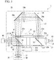
- FIG. 1 is a view illustrating a constitution of a main part of a confocal microscope according to a first embodiment of the present invention.
- a confocal microscope 1 of the present embodiment includes a light source 10, a confocal scanner 20, a microscope 30, and a camera 40 (imaging device).
- Such a confocal microscope 1 generates illumination light (excitation light) for scanning a sample SP using the confocal scanner 20 from light L1 output from the light source 10 and obtains a confocal image of the sample SP irradiated with illumination light using the camera 40.
- the light source 10 outputs the light L1 required for illumination of the sample SP toward the confocal scanner 20.
- the light L1 output from the light source 10 may be coherent light (laser light) or may be incoherent light. In the present embodiment, in order to facilitate understanding, it is assumed that light output from the light source 10 is laser light.
- the light source 10 outputs the light L1 having a wavelength range of 400 to 800 [nm], for example.
- the wavelength range of the light L1 output from the light source 10 is not limited to the foregoing wavelength range (400 to 800 [nm]) and can be an arbitrary wavelength range corresponding to optical characteristics of the sample SP.
- the confocal scanner 20 generates illumination light L4 for scanning the sample SP from the light L1 output from the light source 10 and guides reflected light, fluorescence, or the like (which will hereinafter be simply referred to as "return light” when generically referred to) obtained by irradiating the sample SP with illumination light to the camera 40.
- the confocal scanner 20 includes a collimating lens 21, a disk unit 22, a reflection mirror 23, a split light relay optical system 24 (light guider), a dichroic mirror 25 (beam splitter), an optical filter 26, and a relay lens 27.
- the collimating lens 21 converts the light L1 emitted from the light source 10 into parallel light L2. As illustrated in FIG. 1 , the collimating lens 21 is disposed on an outward side of a microlens array disk 22a and a pinhole array disk 22b in a radial direction such that an optical axis passes through an area between the microlens array disk 22a and the pinhole array disk 22b (which will be described below).
- the light L1 is emitted at a certain spread angle from the light source 10, and the light L1 is converted into the parallel light L2 by the collimating lens 21.
- the collimating lens 21 can be omitted.
- the disk unit 22 generates the illumination light L4 for scanning the sample SP from the parallel light L2 converted by the collimating lens 21.
- the disk unit 22 includes the microlens array disk 22a (first disk), the pinhole array disk 22b (second disk), a rotation shaft 22c (coupling shaft), a motor 22d (driver), and the like.
- the microlens array disk 22a is a disk having a circular plate shape having a plurality of microlenses 22e disposed in a predetermined pattern (for example, spirally disposed at equal pitch).
- the microlens array disk 22a is rotated in a circumferential direction centering on an axis core O illustrated in FIG. 1 .
- the pinhole array disk 22b is a disk having a circular plate shape having a plurality of pinholes 22f formed to be associated with the microlenses 22e of the microlens array disk 22a.
- the microlens array disk 22a and the pinhole array disk 22b are individually connected to the rotation shaft 22c and are disposed so as to face each other with a certain gap therebetween.
- the pinhole array disk 22b is rotated in the circumferential direction centering on the axis core O illustrated in FIG. 1 together with the microlens array disk 22a.
- the rotation shaft 22c is a shaft member to which the microlens array disk 22a and the pinhole array disk 22b are individually fixed and connects the microlens array disk 22a and the pinhole array disk 22b to each other.
- a central part of the microlens array disk 22a is fixed to a tip of the rotation shaft 22c.
- the pinhole array disk 22b is fixed to an intermediate part of the rotation shaft 22c.
- the motor 22d is connected to a root of the rotation shaft 22c.
- the motor 22d is connected to the rotation shaft 22c and generates motive power for rotating the rotation shaft 22c centering on the axis core O.
- the motor 22d rotatably drives the microlens array disk 22a and the pinhole array disk 22b in the circumferential direction centering on the rotation shaft 22c by rotating the rotation shaft 22c. Namely, when the rotation shaft 22c is rotatably driven by the motor 22d, the microlens array disk 22a and the pinhole array disk 22b can integrally rotate around the rotation shaft 22c.
- the motor 22d is disposed on a side of the pinhole array disk 22b opposite to the microlens array disk 22a.
- the motor 22d may be disposed on a side of the microlens array disk 22a opposite to the pinhole array disk 22b.
- the reflection mirror 23 is disposed at a position between the microlens array disk 22a and the pinhole array disk 22b and overlapping the optical axis of the collimating lens 21.
- the reflection mirror 23 reflects the parallel light L2, which is emitted from the collimating lens 21 and is incident between the microlens array disk 22a and the pinhole array disk 22b from the outward side thereof in the radial direction, toward the microlens array disk 22a.
- the reflection mirror 23 reflects the parallel light L2 in a manner parallel to the axis core O of the rotation shaft 22c and guides the parallel light L2 to a surface of the microlens array disk 22a on the pinhole array disk 22b side.
- the parallel light L2 guided to the microlens array disk 22a by the reflection mirror 23 is converted into split light L3 which is split into a plurality of light fluxes by the microlenses 22e.
- the parallel light L2 is incident on the surface of the microlens array disk 22a on the pinhole array disk 22b side, and the split light L3 is emitted from a surface of the microlens array disk 22a on a side opposite to the pinhole array disk 22b.
- the split light relay optical system 24 is an optical system forming a Koehler illumination system in which the microlens array disk 22a serves as an irradiation surface together with the microlenses 22e of the microlens array disk 22a.
- the split light relay optical system 24 includes a reflection mirror 24a, a Fourier lens 24b, and a reflection mirror 24c.
- the reflection mirror 24a is a mirror member on which the split light L3 emitted along the axis core O from the microlens array disk 22a is incident.
- the reflection mirror 24a is a mirror member reflecting the split light L3 such that the optical axis is orthogonal to the axis core O and is directed toward the axis core O.
- the reflection mirror 24a is disposed on a side of the microlens array disk 22a opposite to the pinhole array disk 22b.
- the Fourier lens 24b is a lens on which the split light L3 reflected by the reflection mirror 24a is incident.
- the split light L3 is light which is realized when the parallel light L2 is split into a plurality of light fluxes by the microlens array disk 22a.
- the Fourier lens 24b condenses and spatially superimposes the plurality of light fluxes on an irradiation surface M provided in the microlens array disk 22a. Namely, the Fourier lens 24b is disposed on an optical path of the split light L3 and forms the Koehler illumination system together with the microlenses 22e of the microlens array disk 22a.
- the reflection mirror 24c is a mirror member on which the split light L3 emitted from the Fourier lens 24b is incident.
- the reflection mirror 24c reflects the split light L3 emitted from the Fourier lens 24b in a direction orthogonal to the axis core O such that it is directed toward the microlens array disk 22a.
- the reflection mirror 24c is disposed with the axis core O interposed therebetween.
- the reflection mirror 24a and the reflection mirror 24c guide the split light L3 emitted from the microlens array disk 22a to a side opposite to the pinhole array disk 22b to the surface of the microlens array disk 22a on a side opposite to the pinhole array disk 22b.
- a split light guider which guides the split light L3 to the surface of the microlens array disk 22a on a side opposite to the pinhole array disk 22b is formed by the reflection mirror 24a and the reflection mirror 24c.
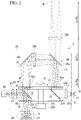
- FIG. 2 is a schematic view illustrating an optical path when the split light L3 is linearly guided without installing the reflection mirror 24a and the reflection mirror 24c in FIG. 1 .
- the microlenses 22e and the Fourier lens 24b are disposed in the Koehler illumination system in which a surface including a main point of the plurality of microlenses 22e serves as the irradiation surface M.
- a rear side focal surface of the microlenses 22e and a front side focal surface of the Fourier lens 24b are disposed so as to coincide with each other.
- a distance (focal distance) f ML from the main point of the microlenses 22e to the rear focal surface is a distance d 1
- a distance (focal distance) f FL from the main point of the Fourier lens 24b to the front focal surface is a distance d 2
- a distance from the main point of the microlenses 22e to the main point of the Fourier lens 24b becomes d 1 +d 2
- the distance (focal distance) f FL from the main point of the Fourier lens 24b to the rear focal surface is a distance d 3
- a distance from the main point of the microlenses 22e to the irradiation surface M becomes d 1 +d 2 +d 3 .
- an optical path length of the split light L3 from the main point of the microlenses 22e through which the split light L3 is emitted to the irradiation surface M becomes d 1 +d 2 +d 3 . Therefore, the optical path length of the split light L3 formed by the split light relay optical system 24 also becomes d 1 +d 2 +d 3 .
- the parallel light L2 is split into a plurality of light fluxes by the microlenses 22e so that it is converted into the split light L3.
- Each of the light fluxes of the split light L3 is converged at a focal point of each of the microlenses 22e, expands again thereafter, is reflected by the reflection mirror 24a, and is directed toward the Fourier lens 24b.
- Each of the light fluxes which has passed through the Fourier lens 24b becomes a parallel beam again and is reflected by the reflection mirror 24c, and a focal surface of the Fourier lens 24b (that is, the irradiation surface M) is irradiated therewith in a superimposed manner.
- the split light L3 becomes the illumination light L4 having a uniform distribution of intensities.
- the plurality of microlenses 22e split the illumination light L4 into a plurality of light fluxes.
- Each of the light fluxes is transmitted through the dichroic mirror 25 and becomes a spot at a focal point position of each of the microlenses 22e.
- the pinhole array disk 22b is disposed at a position on the focal surface of the microlenses 22e, and each of the light fluxes passes through the pinholes 22f associated with the microlenses 22e.
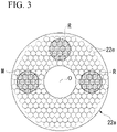
- FIG. 3 is a schematic front view of the microlens array disk 22a.
- a part R where the parallel light L2 emitted from the collimating lens 21 and reflected by the reflection mirror 23 becomes the split light L3 (that is, a part used for Koehler illumination) and the irradiation surface M (a part used for confocal scanning) are provided at different parts in the microlens array disk 22a.
- the reflection mirror 24a and the reflection mirror 24c of the present embodiment are disposed with the axis core O interposed therebetween when viewed in a direction along the axis core O.
- the part R where the parallel light L2 becomes the split light L3 and the irradiation surface M are provided with the axis core O interposed therebetween.
- the split light relay optical system 24 guides the split light L3 such that a position different from an incident position of the parallel light L2 on the microlens array disk 22a serves as the irradiation surface M.
- the part R where the parallel light L2 becomes the split light L3 is not necessarily provided at a position with the axis core O interposed therebetween with respect to the irradiation surface M. For example, as indicated by the two-dot dashed line in FIG.
- the part R where the parallel light L2 becomes the split light L3 may be disposed at a position rotated clockwise by 90° with respect to the irradiation surface M in the circumferential direction centering on the axis core O.
- This rotation angle (90°) is also an example and can be changed.
- the dichroic mirror 25 allows light with which the sample SP is irradiated (illumination light L4) to be transmitted therethrough and reflects return light L5 which is obtained by irradiating the sample SP with the illumination light L4 toward the optical filter 26.
- the dichroic mirror 25 is disposed on the optical axis of the collimating lens 21 and between the microlens array disk 22a and the pinhole array disk 22b provided in the disk unit 22.
- the dichroic mirror 25 is disposed between the microlens array disk 22a and the pinhole array disk 22b.
- the dichroic mirror 25 allows a plurality of light fluxes which have been split and converged by the microlenses 22e provided in the microlens array disk 22a to be transmitted therethrough.
- the light fluxes which have been transmitted through the dichroic mirror 25 are condensed in the pinholes 22f provided in the pinhole array disk 22b, pass through the pinholes 22f, and are emitted to the outside of the disk unit 22.
- the illumination light L4 with which the microlens array disk 22a is irradiated has a uniform distribution of intensities and becomes parallel light
- the illumination light L4 which passes through the pinholes 22f and is emitted to the outside of the disk unit 22 also has a uniform distribution of intensities.
- the dichroic mirror 25 reflects the return light L5 which has been transmitted through the pinholes 22f provided in the pinhole array disk 22b toward the optical filter 26 disposed on the outward side in the radial direction centering on the axis core O.
- the dichroic mirror 25 allows light with which the microlens array disk 22a is irradiated via the split light relay optical system 24 and which has passed through the microlenses 22e (illumination light L4) to be transmitted therethrough and reflects light incident from the pinhole array disk 22b side (return light) toward the outward side of the microlens array disk 22a and the pinhole array disk 22b in the radial direction.
- the optical filter 26 filters the return light L5 reflected by the dichroic mirror 25.
- a polarizing filter, an absorption filter (emission filter), a dichroic mirror, or the like can be used.
- the relay lens 27 is disposed between the optical filter 26 and the camera 40 and guides the return light L5 emitted from the optical filter 26 to the camera 40.
- the microscope 30 irradiates the sample SP with illumination light generated in the disk unit 22 and guides the return light L5 obtained by irradiating the sample SP with the illumination light L4 to the disk unit 22.
- the microscope 30 is an infinite distance correction optical system including an object lens 31.
- the sample SP is illustrated inside the microscope 30, but it should be noted that the sample SP does not constitute the microscope 30 and the sample SP can be replaced.
- the camera 40 images a confocal image of the sample SP which is irradiated with the illumination light L4.
- this camera 40 is a camera including a solid-state imaging device such as a charge coupled device (CCD) or a complementary metal oxide semiconductor (CMOS) and is capable of imaging a two-dimensional still image or a moving image.
- CMOS complementary metal oxide semiconductor
- a display device may display a confocal image of the sample SP obtained by the camera 40.
- light output from the light source 10 When operation of the confocal microscope 1 starts, light is output from the light source 10, and the disk unit 22 starts to rotate (rotate around the rotation shaft 22c).
- the light L1 output from the light source 10 is input to the confocal scanner 20. It is assumed that light output from the light source 10 is light having a distribution of intensities (for example, light having a Gaussian distribution).
- the light L1 input to the confocal scanner 20 incident on the collimating lens 21 is converted into the parallel light L2 by the collimating lens 21.
- the parallel light L2 is incident between the microlens array disk 22a and the pinhole array disk 22b from the collimating lens 21.
- the parallel light L2 is reflected toward the microlens array disk 22a by the reflection mirror 23 disposed between the microlens array disk 22a and the pinhole array disk 22b.
- the parallel light L2 with which the microlens array disk 22a is irradiated is split into a plurality of light fluxes by the microlenses 22e provided in the microlens array disk 22a and is converted into the split light L3 constituted of a plurality of light fluxes.
- the split light L3 is emitted through the microlenses 22e and is reflected toward the Fourier lens 24b by the reflection mirror 24a.
- each of the light fluxes is a parallel beam.
- These light fluxes are converted into light fluxes which are superimposed on the irradiation surface M.
- the split light L3 emitted from the Fourier lens 24b is reflected toward the reflection mirror 24c and is used for irradiating the irradiation surface M including the main point of the plurality of microlenses 22e.
- the microlenses 22e and the Fourier lens 24b form the Koehler illumination system in which a flat surface including the main point of the plurality of microlenses 22e serves as the irradiation surface M.
- a flat surface including the main point of the plurality of microlenses 22e serves as the irradiation surface M.
- the illumination light L4 is split into a plurality of light fluxes by the plurality of microlenses 22e. Each of the light fluxes is converged by the microlenses 22e and passes through the pinholes 22f of the pinhole array disk 22b. At this time, the illumination light L4 emitted through the microlenses 22e is transmitted through the dichroic mirror 25 and is incident on the pinhole array disk 22b. The illumination light L4 emitted through the pinholes 22f is emitted to the outside of the disk unit 22.
- the illumination light L4 emitted to the outside of the disk unit 22 is used for irradiating the sample SP via the object lens 31 provided in the microscope 30.
- the illumination light L4 emitted to the outside of the disk unit 22 is obtained by splitting light having a uniformized distribution of intensities. For this reason, the sample SP is irradiated with illumination light having a uniformized distribution of intensities.
- the return light L5 (return light obtained by irradiating the sample SP with illumination light) from the sample SP is incident on the disk unit 22 via the object lens 31 provided in the microscope 30. Further, the return light L5 goes through the pinholes 22f formed in the pinhole array disk 22b of the disk unit 22 and then is reflected toward the optical filter 26 by the dichroic mirror 25.
- the return light L5 reflected by the dichroic mirror 25 is incident on the camera 40 via the optical filter 26 and the relay lens 27 in this order and forms an image.
- the illumination light L4 for irradiating the sample SP is used for scanning in accordance with rotation of the disk unit 22. Accordingly, the return light L5 corresponding to a scanning position of the illumination light L4 is successively input to the camera 40. In this manner, a confocal image of the sample SP is obtained by the camera 40.
- the confocal scanner 20 includes the microlens array disk 22a which has the plurality of microlenses 22e and is rotated.
- the confocal scanner 20 includes the pinhole array disk 22b.
- the pinhole array disk 22b has the plurality of pinholes 22f formed to be associated with the microlenses 22e.
- the pinhole array disk 22b is disposed so as to face the microlens array disk 22a and is rotated together with the microlens array disk 22a.
- the confocal scanner 20 includes the split light relay optical system 24.
- the split light relay optical system 24 forms the Koehler illumination system in which the microlens array disk 22a serves as the irradiation surface M together with the microlenses 22e.
- the split light relay optical system 24 guides the split light L3 formed from the parallel light L2 which has been split into a plurality of light fluxes through the microlenses 22e to the irradiation surface M.
- the confocal scanner 20 includes the dichroic mirror 25.
- the dichroic mirror 25 is disposed between the microlens array disk 22a and the pinhole array disk 22b.
- the dichroic mirror 25 allows light with which the microlens array disk 22a is irradiated via the split light relay optical system 24 and which has passed through the microlenses 22e to be transmitted therethrough.
- the dichroic mirror 25 reflects light incident from the pinhole array disk 22b side toward the outward side of the microlens array disk 22a and the pinhole array disk 22b in the radial direction.
- the Koehler illumination system is formed by the microlenses 22e of the microlens array disk 22a and the split light relay optical system 24.
- the microlens array disk 22a and the motor 22d serve as both constituent elements for the confocal scanner generating the illumination light L4 and constituent elements for the homogenizer uniformizing a distribution of intensities of the illumination light L4. For this reason, according to the confocal scanner 20, there is no need to separately provide all the constituent elements for the homogenizer.
- the sample SP can be irradiated with the illumination light L4 having a uniform distribution of intensities, and a confocal image having a homogeneous brightness with no unevenness can be obtained.
- the split light relay optical system 24 guides the split light L3 such that a position different from the incident position of the parallel light L2 on the microlens array disk 22a serves as the irradiation surface M. Namely, in the confocal scanner 20, the distribution of intensities is uniformized at a part of the microlens array disk 22a which is not used when only the illumination light L4 is generated. Therefore, a space for disposing the microlenses 22e of the microlens array disk 22a can be effectively utilized.
- the split light relay optical system 24 includes the reflection mirror 24a and the reflection mirror 24c which function as the split light guiders.
- the reflection mirror 24a and the reflection mirror 24c guide the split light L3 emitted from the microlens array disk 22a to a side opposite to the pinhole array disk 22b to the surface of the microlens array disk 22a on a side opposite to the pinhole array disk 22b.
- the split light relay optical system 24 includes the Fourier lens 24b which is disposed on the optical path of the split light L3 and forms the Koehler illumination system together with the microlenses 22e.
- the split light L3 is emitted from the microlens array disk 22a to a side opposite to the pinhole array disk 22b.
- the split light L3 is guided from the microlens array disk 22a to a side opposite to the pinhole array disk 22b.
- the light source 10 can be disposed on the outward side of the microlens array disk 22a and the pinhole array disk 22b in the radial direction.
- the dimension of the confocal scanner 20 in a direction along the axis core O can be reduced.
- the confocal scanner 20 includes the rotation shaft 22c which connects the microlens array disk 22a and the pinhole array disk 22b to each other, and the motor 22d which rotatably drives the rotation shaft 22c.
- the microlens array disk 22a and the pinhole array disk 22b can be rotatably driven with the single motor 22d. Therefore, in the confocal scanner 20, increase in device size and cost rise are further curbed.
- the confocal microscope 1 includes the confocal scanner 20 which emits the illumination light L4 for scanning the sample SP, the light source 10 which outputs light toward the confocal scanner 20, and the camera 40 which images a confocal image of the sample SP irradiated with the illumination light L4.
- the confocal scanner 20 while increase in device size and cost rise are curbed, a distribution of intensities of light emitted from the confocal scanner 20 can be uniformized.
- the sample SP can be irradiated with the illumination light L4 having a uniform distribution of intensities, and a confocal image having a homogeneous brightness with no unevenness can be obtained.
- FIG. 4 is a view illustrating a constitution of a main part of a confocal microscope according to a second embodiment of the present invention.
- the same reference signs are applied to the same constitution as the constitution illustrated in FIG. 1 .
- a confocal microscope 2 of the present embodiment has a constitution in which the confocal scanner 20 of the confocal microscope 1 illustrated in FIG. 1 is replaced with a confocal scanner 20A and disposition of the light source 10 is changed.
- the light source 10 is disposed on a side of the microlens array disk 22a opposite to the pinhole array disk 22b.
- the collimating lens 21 is disposed between the light source 10 and the microlens array disk 22a.
- the parallel light L2 is incident on the surface of the microlens array disk 22a on a side opposite to the pinhole array disk 22b.
- the split light L3 is emitted from the surface of the microlens array disk 22a on the pinhole array disk 22b side toward the pinhole array disk 22b.
- the reflection mirror 23 included in the confocal scanner 20 illustrated in FIG. 1 is not provided, and a split light relay optical system 24A is provided in place of the split light relay optical system 24.
- the split light relay optical system 24A includes a plurality of reflection mirrors for guiding the split light L3 emitted from the microlens array disk 22a toward the pinhole array disk 22b to the surface of the microlens array disk 22a on a side opposite to the pinhole array disk 22b.
- the split light relay optical system 24A includes a reflection mirror 24d which is disposed between the microlens array disk 22a and the pinhole array disk 22b. This reflection mirror 24d reflects the split light L3 emitted from the microlens array disk 22a toward the outward side of the microlens array disk 22a in the radial direction.
- the split light relay optical system 24A includes a reflection mirror 24e which is disposed on the outward side of the microlens array disk 22a and the pinhole array disk 22b in the radial direction.
- This reflection mirror 24e reflects the split light L3 which has been reflected by the reflection mirror 24d to the outward side of the microlens array disk 22a and the pinhole array disk 22b in the radial direction.
- the reflection mirror 24e reflects the split light L3 such that the optical path of the split light L3 becomes parallel to the axis core O and is directed toward the light source 10.
- the split light relay optical system 24A includes a reflection mirror 24f which is disposed in the middle of the optical path of the split light L3 and between the reflection mirror 24e and the Fourier lens 24b. This reflection mirror 24f reflects the split light L3 incident from the reflection mirror 24e in directions orthogonal to the axis core O and directed toward the axis core O.
- the split light relay optical system 24A includes a reflection mirror 24g which is disposed in the middle of the optical path of the split light L3 and between the Fourier lens 24b and the irradiation surface M. This reflection mirror 24g is disposed with the axis core O interposed between the reflection mirror 24g and the reflection mirror 24f when viewed in a direction along the axis core O.
- the reflection mirror 24d, the reflection mirror 24e, the reflection mirror 24f, and the reflection mirror 24g form a split light guider which guides the split light L3 emitted from the microlens array disk 22a toward the pinhole array disk 22b to the surface of the microlens array disk 22a on a side opposite to the pinhole array disk 22b.
- the parallel light L2 is incident on the surface of the microlens array disk 22a on a side opposite to the pinhole array disk 22b.
- the split light L3 guided by the split light relay optical system 24A is incident on the surface of the microlens array disk 22a on a side opposite to the pinhole array disk 22b.
- both the parallel light L2 and the split light L3 are incident on the same surface of the microlens array disk 22a.
- the confocal scanner 20A of the present embodiment includes the split light relay optical system 24A.
- the split light relay optical system 24A includes the reflection mirror 24d, the reflection mirror 24e, the reflection mirror 24f, and the reflection mirror 24g forming the split light guider. These reflection mirrors reflect the split light L3 emitted from the microlens array disk 22a to the pinhole array disk 22b side toward the outward side of the microlens array disk 22a and the pinhole array disk 22b in the radial direction from between the microlens array disk 22a and the pinhole array disk 22b. In addition, these reflection mirrors guide the split light L3 to the surface of the microlens array disk 22a on a side opposite to the pinhole array disk 22b. Moreover, the split light relay optical system 24A includes the Fourier lens 24b which is disposed on the optical path of the split light L3 and forms the Koehler illumination system together with the microlenses 22e.
- both the parallel light L2 and the split light L3 are incident on the same surface of the microlens array disk 22a.
- design of the microlenses 22e becomes simple, and the microlenses 22e having a small aberration can be easily realized.
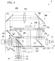
- FIG. 5 is a view illustrating a constitution of a main part of a confocal microscope according to a third embodiment of the present invention.
- the same reference signs are applied to the same constitution as the constitution illustrated in FIG. 1 .
- a confocal microscope 3 of the present embodiment has a constitution in which the confocal scanner 20 of the confocal microscope 1 illustrated in FIG. 1 is replaced with a confocal scanner 20B.
- the confocal scanner 20B includes a disk unit 22B in place of the disk unit 22.
- the disk unit 22B includes a second microlens array disk 22g in addition to the microlens array disk 22a and the pinhole array disk 22b.
- the second microlens array disk 22g is a disk having a circular plate shape having a plurality of second microlenses 22h disposed in a predetermined pattern (for example, spirally disposed at equal pitch). These second microlenses 22h are formed to be associated with the microlenses 22e of the microlens array disk 22a.
- the second microlens array disk 22g is disposed a side opposite to the pinhole array disk 22b with respect to the microlens array disk 22a and faces the microlens array disk 22a with a certain gap therebetween.
- the second microlens array disk 22g is connected to the microlens array disk 22a through the rotation shaft 22c and is rotated in the circumferential direction centering on the axis core O together with the microlens array disk 22a.
- Such a second microlens array disk 22g is disposed on the focal surface of the microlenses 22e of the microlens array disk 22a.
- Each of the second microlenses 22h in the second microlens array disk 22g is disposed on the rear focal surface of the associated microlenses 22e.
- the confocal scanner 20B includes a split light relay optical system 24B in place of the split light relay optical system 24 of the confocal scanner 20.
- the split light relay optical system 24B includes a plurality of reflection mirrors for guiding the split light L3 emitted from the second microlens array disk 22g to the surface of the microlens array disk 22a on a side opposite to the pinhole array disk 22b.
- the split light relay optical system 24B includes a reflection mirror 24h which is disposed on a side of the second microlens array disk 22g opposite to the microlens array disk 22a. This reflection mirror 24h reflects the incident split light L3 in directions orthogonal to the axis core O and directed toward the axis core O.
- the split light relay optical system 24B includes a reflection mirror 24i which is disposed with the axis core O interposed therebetween when viewed in a direction along the axis core O. As illustrated in FIG.
- this reflection mirror 24i is disposed on the outward side of the disk unit 22B and reflects the split light L3 incident from the reflection mirror 24i via a Fourier lens 24m (which will be described below) in directions parallel to the axis core O and directed toward the microlens array disk 22a.
- the split light relay optical system 24B includes a reflection mirror 24j which is disposed on the outward side of the disk unit 22B and between the microlens array disk 22a and the second microlens array disk 22g in a direction along the axis core O.
- This reflection mirror 24j reflects the split light L3 incident from the reflection mirror 24i toward an inward side of the microlens array disk 22a in the radial direction.
- the split light relay optical system 24B includes a reflection mirror 24k which is disposed between the microlens array disk 22a and the second microlens array disk 22g. This reflection mirror 24k reflects the illumination light L4 incident from the reflection mirror 24j to the surface of the microlens array disk 22a on a side opposite to the pinhole array disk 22b.
- the reflection mirror 24h, the reflection mirror 24i, the reflection mirror 24j, and the reflection mirror 24k form a split light guider which guides the split light L3 emitted from the microlens array disk 22a and having passed through the second microlens array disk 22g to the surface of the microlens array disk 22a on a side opposite to the pinhole array disk 22b.
- the split light relay optical system 24B includes the Fourier lens 24m which is disposed between the reflection mirror 24h and the reflection mirror 24i.
- the Fourier lens 24m is disposed such that the front focal surface of the Fourier lens 24m overlaps the main point of the second microlenses 22h of the second microlens array disk 22g.
- the microlenses 22e, the second microlenses 22h, and the Fourier lens 24m form the Koehler illumination system in which the microlens array disk 22a serves as the irradiation surface M.
- each of the light fluxes of the split light L3 is converged at the focal point of each of the microlenses 22e (that is, the second microlenses 22h), expands again thereafter, and becomes a parallel beam again by the Fourier lens 24m, and the irradiation surface M is irradiated therewith in a superimposed manner.
- the split light L3 becomes the illumination light L4 having a uniform distribution of intensities.
- the distribution of intensities of the split light L3 with which the irradiation surface M is irradiated can be further uniformized.
- the microlenses 22e and the second microlenses 22h may have perfectly the same shape but may have different properties.
- the confocal scanner 20B of the present embodiment includes the second microlens array disk 22g.
- the second microlens array disk 22g has the plurality of second microlenses 22h formed to be associated with the microlenses 22e.
- the second microlens array disk 22g is disposed so as to face the microlens array disk 22a and is rotated from a side opposite to the pinhole array disk 22b.
- the split light relay optical system 24B includes the Fourier lens 24m.
- the Fourier lens 24m is disposed on the optical path of the split light L3 and forms the Koehler illumination system together with the microlenses 22e and the second microlenses 22h.
- the split light relay optical system 24B includes the reflection mirrors (the reflection mirror 24h, the reflection mirror 24i, the reflection mirror 24j, and the reflection mirror 24k) which function as the split light guiders. These reflection mirrors guide the split light L3 emitted from the microlens array disk 22a to the second microlens array disk 22g side and transmitted through the second microlens array disk 22g to the surface of the microlens array disk 22a on a side opposite to the pinhole array disk 22b.
- reflection mirrors the reflection mirror 24h, the reflection mirror 24i, the reflection mirror 24j, and the reflection mirror 24k
- FIG. 6 is a view illustrating a constitution of a main part of a confocal microscope according to a fourth embodiment of the present invention.
- the same reference signs are applied to the same constitution as the constitution illustrated in FIG. 1 .
- a confocal microscope 4 of the present embodiment has a constitution in which the confocal scanner 20 of the confocal microscope 1 illustrated in FIG. 1 is replaced with a confocal scanner 20C and disposition of the light source 10 is changed.
- the light source 10 is disposed on a side of the microlens array disk 22a opposite to the pinhole array disk 22b.
- the light L1 emitted from the light source 10 is linearly polarized light (P-polarized light).
- the collimating lens 21 is disposed between the light source 10 and the microlens array disk 22a.
- the parallel light L2 is incident on the surface of the microlens array disk 22a on a side opposite to the pinhole array disk 22b.
- the split light L3 is emitted from the surface of the microlens array disk 22a on the pinhole array disk 22b side toward the pinhole array disk 22b.
- the reflection mirror 23 included in the confocal scanner 20 illustrated in FIG. 1 is not provided, and a split light relay optical system 24C is provided in place of the split light relay optical system 24.
- the split light relay optical system 24C includes a polarization beam splitter 24p, a 1/4 wavelength plate 24q, a split light reflection mirror 24r, and a reflection mirror 24s.
- the polarization beam splitter 24p is disposed between the collimating lens 21 and the microlens array disk 22a, allows P-polarized light to be transmitted therethrough, and reflects S-polarized light toward the Fourier lens 24b.
- the polarization beam splitter 24p allows the parallel light L2 to be transmitted therethrough.
- the split light L3 incident on the polarization beam splitter 24p is S-polarized light. For this reason, the polarization beam splitter 24p reflects the incident split light L3.
- the 1/4 wavelength plate 24q is disposed between the polarization beam splitter 24p and the microlens array disk 22a.
- the 1/4 wavelength plate 24q is an optical element for changing a phase of incident light by a 1/4 wavelength and emitting the light.
- the 1/4 wavelength plate 24q converts the parallel light L2 of incident P-polarized light transmitted through the polarization beam splitter 24p into circularly polarized light and emits the light.
- the 1/4 wavelength plate 24q converts the split light L3 of circularly polarized light incident from the microlens array disk 22a into S-polarized light and emits the light.
- the split light reflection mirror 24r is disposed between the microlens array disk 22a and the pinhole array disk 22b and reflects the split light L3 emitted from the microlens array disk 22a to the pinhole array disk 22b side again toward the 1/4 wavelength plate 24q via the microlens array disk 22a.
- This split light reflection mirror 24r is disposed at a position at half the focal distance of the microlenses 22e from the microlens array disk 22a.
- the reflection mirror 24s is disposed so as to face the polarization beam splitter 24p with the Fourier lens 24b interposed therebetween. When viewed in a direction along the axis core O, the reflection mirror 24s is disposed at a position with the axis core O interposed between the reflection mirror 24s and the polarization beam splitter 24p.
- This reflection mirror 24s reflects the split light L3 of S-polarized light reflected by the polarization beam splitter 24p toward the irradiation surface M.
- Such a reflection mirror 24s functions as a split light guider for guiding the split light L3 reflected by the polarization beam splitter 24p to the surface of the microlens array disk 22a on a side opposite to the pinhole array disk 22b.
- the parallel light L2 which has become P-polarized light is transmitted through the polarization beam splitter 24p and is converted into circularly polarized light by the 1/4 wavelength plate 24q.
- the parallel light L2 which has been converted into circularly polarized light is incident on the microlens array disk 22a and is converted into the split light L3.
- the split light L3 emitted from the microlens array disk 22a toward the pinhole array disk 22b is reflected toward the 1/4 wavelength plate 24q by the split light reflection mirror 24r.
- the split light L3 reflected by the 1/4 wavelength plate 24q is transmitted through the microlens array disk 22a again and is converted into S-polarized light by the 1/4 wavelength plate 24q.
- the split light L3 converted into S-polarized light by the 1/4 wavelength plate 24q is reflected by the polarization beam splitter 24p, and the irradiation surface M is irradiated therewith via the Fourier lens 24b and the reflection mirror 24s.
- the parallel light L2 is P-polarized light.
- the split light relay optical system 24C includes the polarization beam splitter 24p which reflects the split light L3 and allows the parallel light L2 to be transmitted therethrough, and the 1/4 wavelength plate 24q which is disposed between the polarization beam splitter 24p and the microlens array disk 22a.
- the split light relay optical system 24C includes the split light reflection mirror 24r. The split light reflection mirror 24r reflects the split light L3 emitted from the microlens array disk 22a to the pinhole array disk 22b side toward the 1/4 wavelength plate via the microlens array disk 22a.
- the split light relay optical system 24C includes the reflection mirror 24s for guiding the split light L3 reflected by the polarization beam splitter 24p to the surface of the microlens array disk 22a on a side opposite to the pinhole array disk 22b.
- the split light relay optical system 24C includes the Fourier lens 24b which is disposed on the optical path of the split light L3 and forms the Koehler illumination system together with the microlenses 22e.
- the split light L3 is caused to pass through one microlens array disk 22a twice between the 1/4 wavelength plate 24q and the split light reflection mirror 24r. For this reason, the distribution of intensities of the illumination light L4 can be further uniformized than when the split light L3 is caused to pass through the microlens array disk 22a only once.
- the confocal scanner and the confocal microscope according to the embodiments of the present invention have been described, but the present invention is not limited to the foregoing embodiments and can be freely changed within the scope of the present invention.
- the microlens array disk 22a may be increased in diameter such that the microlens array disk 22a covers the reflection mirror 24e when viewed in a direction along the axis core O.
- the intensity of the illumination light L4 can be further uniformized by increasing the number of times of causing the split light L3 to pass through the microlens array disk 22a.
- the light L1 emitted from the light source 10 is P-polarized light
- the light L1 output from the light source 10 may be S-polarized light.
- the polarization beam splitter 24p allows S-polarized light to be transmitted therethrough and reflects P-polarized light.
- the term "configured” is used to describe a component, unit or part of a device includes hardware and/or software that is constructed and/or programmed to carry out the desired function.
- unit is used to describe a component, unit or part of a hardware and/or software that is constructed and/or programmed to carry out the desired function.
- Typical examples of the hardware may include, but are not limited to, a device and a circuit.
Landscapes
- Physics & Mathematics (AREA)
- General Physics & Mathematics (AREA)
- Optics & Photonics (AREA)
- Chemical & Material Sciences (AREA)
- Analytical Chemistry (AREA)
- Microscoopes, Condenser (AREA)
Abstract
Description
- The present invention relates to a confocal scanner and a confocal microscope.
- Priority is claimed on
Japanese Patent Application No. 2021-041637, filed on March 15, 2021 - In the related art, a confocal microscope using a disk scanning-type confocal scanner has been developed. In this confocal microscope, a confocal scanner including a microlens array disk which has a plurality of microlenses formed in a predetermined pattern and a pinhole array disk which has a plurality of pinholes associated with the respective microlenses and formed in the same pattern as the microlenses and is constituted to be able to rotate together with the microlens array disk is used.
- In such a confocal microscope, a confocal image of a sample can be obtained by rotating disks (a microlens array disk and a pinhole array disk) provided in a confocal scanner and changing an irradiation position of laser light with respect to the sample (scanning a sample with laser light).
Japanese Patent No. 2663780 Japanese Unexamined Patent Application Publication No. 2019-174586 - The homogenizer disclosed in
Japanese Unexamined Patent Application Publication No. 2019-174586 Japanese Unexamined Patent Application Publication No. 2019-174586 Japanese Patent No. 2663780 Japanese Unexamined Patent Application Publication No. 2019-174586 Japanese Patent No. 2663780 - In order to resolve the foregoing problem, a confocal scanner (20, 20A, 20B, or 20C) according to an aspect of the present invention may include: a first disk (22a) which includes a plurality of microlenses (22e); a second disk (22b) which includes a plurality of pinholes (22f) formed to be associated with the microlenses, wherein one surface (A1) of the first disk faces another surface (B2) of the second disk, and the second disk rotates together with the first disk; a light guider (24, 24A, 24B, or 24C) which forms a Koehler illumination system together with the microlenses within a first region (R) set in the first disk, wherein the light guider guides a plurality of rays of split light (L3) split by the microlenses within the first region to a second region (M) set in the first disk; and a beam splitter (25) which is disposed between the one surface (A1) of the first disk and the another surface (B2) of the second disk, wherein light which has passed through the microlenses within the second region transmits through the beam splitter, and the beam splitter reflects light incident from the second disk toward an outward side of the first disk and the second disk in a radial direction.
- In addition, in the confocal scanner according to the aspect of the present invention, the first region and the second region are at different positions on the first disk.
- In addition, in the confocal scanner according to the aspect of the present invention, the light guider may include: a split light guider which guides split light emitted from another surface (B1) of the first disk in a direction of the another surface (B1) of the first disk; and a Fourier lens (24b or 24m) which is disposed on an optical path of the split light and forms a part of the Koehler illumination system.
- In addition, in the confocal scanner according to the aspect of the present invention, the light guider may include: a split light guider which reflects split light emitted from the one surface (A1) of the first disk to the second disk toward the outward side of the first disk and the second disk in the radial direction from between the one surface (A1) of the first disk and the another surface (B2) of the second disk, wherein the split light guider guides the reflected light in a direction of another surface (B1) of the first disk; and a Fourier lens which is disposed on an optical path of the split light and forms a part of the Koehler illumination system.
- In addition, the confocal scanner according to the aspect of the present invention further may include: a third disk (22g) which includes a plurality of second microlenses (22h) formed to be associated with the microlenses, wherein one surface (A3) of the third disk faces another surface (B1) of the first disk, and the third disk rotates together with the first disk and the second disk. The light guider may include: a split light guider which guides split light, which has emitted from the another surface (B1) of the first disk to the third disk and transmitted through the third disk, in a direction of the another surface (B1) of the first disk; and a Fourier lens which is disposed on an optical path of the split light and forms a part of the Koehler illumination system.
- In addition, in the confocal scanner according to the aspect of the present invention, the light guider may include: a polarization beam splitter (24p), wherein polarized light incident on the first region transmits through the polarization beam splitter, and the polarization beam splitter reflects the split light; a 1/4 wavelength plate (24q) which is disposed between the polarization beam splitter and the first disk; a reflection mirror (24r) which reflects the split light emitted from the one surface (A1) of the first disk to the second disk toward the 1/4 wavelength plate via the first disk; a split light guider which guides the split light reflected by the polarization beam splitter to another surface (B1) of the first disk; and a Fourier lens which is disposed on an optical path of the split light and forms a part of the Koehler illumination system.
- In addition, the confocal scanner according to the aspect of the present invention further may include: a coupling shaft (22c) which connects the first disk and the second disk to each other; and a driver (22d) which rotatably drives the coupling shaft.
- In addition, the confocal scanner according to the aspect of the present invention further may include: an optical filter (26) which filters the light reflected by the beam splitter; and a relay lens (27) which forms an image of the light emitted from the optical filter.
- In addition, the confocal scanner according to the aspect of the present invention further may include: a collimating lens (21) which converts light emitted from a light source into parallel light; and a reflection mirror (23) which reflects the parallel light, which has been emitted from the collimating lens, toward the first disk.
- In addition, in the confocal scanner according to the aspect of the present invention, the collimating lens is disposed on the outward side of the first disk and the second disk in the radial direction such that an optical axis of the parallel light passes through an area between the first disk and the second disk.
- A confocal microscope according to another aspect of the present invention may include: the confocal scanner according to any one of those described above, which emits illumination light for scanning a sample; a light source (10) which outputs light for generating the illumination light; and an imaging device (40) which images a confocal image of the sample.
- In addition, in the confocal microscope according to the aspect of the present invention, the first region and the second region are at different positions on the first disk.
- In addition, in the confocal microscope according to the aspect of the present invention, the light guider may include: a split light guider which guides split light emitted from another surface of the first disk in a direction of the another surface of the first disk; and a Fourier lens which is disposed on an optical path of the split light and forms a part of the Koehler illumination system.
- In addition, in the confocal microscope according to the aspect of the present invention, the light guider may include: a split light guider which reflects split light emitted from the one surface of the first disk to the second disk toward the outward side of the first disk and the second disk in the radial direction from between the one surface of the first disk and the another surface of the second disk, wherein the split light guider guides the reflected light in a direction of another surface of the first disk; and a Fourier lens which is disposed on an optical path of the split light and forms a part of the Koehler illumination system.
- In addition, in the confocal microscope according to the aspect of the present invention, the confocal scanner may further include: a third disk which includes a plurality of second microlenses formed to be associated with the microlenses, wherein one surface of the third disk faces another surface of the first disk, and the third disk rotates together with the first disk and the second disk. The light guider may further include: a split light guider which guides split light, which has emitted from the another surface of the first disk to the third disk and transmitted through the third disk, in a direction of the another surface of the first disk; and a Fourier lens which is disposed on an optical path of the split light and forms a part of the Koehler illumination system.
- In addition, in the confocal microscope according to the aspect of the present invention, the light guider may include: a polarization beam splitter, wherein polarized light incident on the first region transmits through the polarization beam splitter, and the polarization beam splitter reflects the split light; a 1/4 wavelength plate which is disposed between the polarization beam splitter and the first disk; a reflection mirror which reflects the split light emitted from the one surface of the first disk to the second disk toward the 1/4 wavelength plate via the first disk; a split light guider which guides the split light reflected by the polarization beam splitter to another surface of the first disk; and a Fourier lens which is disposed on an optical path of the split light and forms a part of the Koehler illumination system.
- In addition, in the confocal microscope according to the aspect of the present invention, the confocal scanner may further include: a coupling shaft which connects the first disk and the second disk to each other; and a driver which rotatably drives the coupling shaft.
- In addition, in the confocal microscope according to the aspect of the present invention, the confocal scanner may further include: an optical filter which filters the light reflected by the beam splitter; and a relay lens which forms an image of the light emitted from the optical filter.
- In addition, in the confocal microscope according to the aspect of the present invention, the confocal scanner may further include: a collimating lens which converts light emitted from a light source into parallel light; and a reflection mirror which reflects the parallel light, which has been emitted from the collimating lens, toward the first disk.
- In addition, in the confocal microscope according to the aspect of the present invention, the collimating lens is disposed on the outward side of the first disk and the second disk in the radial direction such that an optical axis of the parallel light passes through an area between the first disk and the second disk.
- According to the present invention, it is possible to achieve an effect in which increase in device size and cost rise can be curbed and a confocal image having a uniform brightness and high image quality can be obtained.
- Further features and aspects of the present disclosure will become apparent from the following detailed description of exemplary embodiments with reference to the attached drawings.
-
-
FIG. 1 is a view illustrating a constitution of a main part of a confocal microscope according to a first embodiment of the present invention. -
FIG. 2 is a schematic view illustrating an optical path when split light is linearly guided without installing reflection mirrors inFIG. 1 . -
FIG. 3 is a schematic front view of a microlens array disk according to the first embodiment of the present invention. -
FIG. 4 is a view illustrating a constitution of a main part of a confocal microscope according to a second embodiment of the present invention. -
FIG. 5 is a view illustrating a constitution of a main part of a confocal microscope according to a third embodiment of the present invention. -
FIG. 6 is a view illustrating a constitution of a main part of a confocal microscope according to a fourth embodiment of the present invention. - The embodiments of the present invention will be now described herein with reference to illustrative preferred embodiments. Those skilled in the art will recognize that many alternative preferred embodiments can be accomplished using the teaching of the present invention and that the present invention is not limited to the preferred embodiments illustrated herein for explanatory purposes.
- An aspect of the present invention is to provide a confocal scanner and a confocal microscope in which increase in device size and cost rise can be curbed and a confocal image having a uniform brightness and high image quality can be obtained.
- Hereinafter, a confocal scanner and a confocal microscope according to embodiments of the present invention will be described in detail with reference to the drawings. Hereinafter, first, an overview of the embodiments of the present invention will be described. Subsequently, details of each of the embodiments of the present invention will be described.
- The embodiments of the present invention provide a confocal scanner and a confocal microscope in which increase in device size and cost rise can be curbed and a confocal image having a uniform brightness and high image quality can be obtained. Here, the confocal microscope can be applied to a product such as a drug development support device utilizing a confocal laser microscopic method. In the foregoing product, for example, a laser light source which can be regarded as a point light source is expanded with a collimating lens or the like such that it becomes a two-dimensional surface light source. Further, the sample is excited by irradiating a sample such as a cell with the surface light source via an optical system of the confocal scanner. The cell has been fused with a fluorescent material in advance so that the cell emits fluorescence when excitation light is received. This fluorescence is imaged as an image using a microscopic optical system, and observation of the cell or analysis of behavior of the cell is performed. Such a confocal microscope is utilized in the fields of basic research on living beings to application/development of drug discovery.
- When a cell image is imaged, in order to obtain high image quality with no blur, a confocal method is utilized in the optical system. In addition, in order to uniformize a brightness of an image throughout the entire surface, it is preferable to use a homogenizer which uniformizes an intensity of illumination light (excitation light) throughout the entire surface. The embodiments of the present invention include two technologies, such as a technology for a confocal scanner realizing a confocal microscopic method and a technology for a homogenizer uniformizing illumination light.
- Each of the technology for a confocal scanner realizing a confocal microscopic method and the technology for a homogenizer uniformizing illumination light will be described.
-
Japanese Patent No. 2663780 - A disk unit is formed by the light condensing disk, the pinhole disk, and a drum (coupling shaft) which couples these to each other. The disk unit is attached to a motor and is rotatably driven. A confocal optical scanner is constituted of this disk unit and a beam splitter. When the disk unit is rotated by means of the motor, the function of the confocal scanner is realized.
-
Japanese Unexamined Patent Application Publication No. 2019-174586 Japanese Unexamined Patent Application Publication No. 2019-174586 - In order to realize a confocal scanner having uniformized illumination light, for example, a method of joining the devices in
Japanese Patent No. 2663780 Japanese Unexamined Patent Application Publication No. 2019-174586 Japanese Patent No. 2663780 Japanese Unexamined Patent Application Publication No. 2019-174586 Japanese Patent No. 2663780 Japanese Patent No. 2663780 Japanese Unexamined Patent Application Publication No. 2019-174586 - The confocal scanner according to the embodiment of the present invention includes a first disk which has a plurality of microlenses and is rotated. In addition, the confocal scanner includes a second disk. The second disk has a plurality of pinholes formed to be associated with the microlenses. In addition, the second disk is disposed so as to face the first disk and is rotated together with the first disk.
- In addition, the confocal scanner according to the embodiment of the present invention includes a light guider. The light guider forms the Koehler illumination system in which the first disk serves as an irradiation surface together with the microlenses. In addition, the light guider guides split light formed from parallel light which has been split into a plurality of light fluxes through the microlenses to the irradiation surface.
- Moreover, the confocal scanner according to the embodiment of the present invention includes a beam splitter. The beam splitter is disposed between the first disk and the second disk. In addition, the beam splitter allows light with which the first disk is irradiated via the light guider and which has passed through the microlenses to be transmitted therethrough. In addition, the beam splitter reflects light incident from the second disk side toward an outward side of the first disk and the second disk in a radial direction.
- In such a confocal scanner according to the embodiment of the present invention, the Koehler illumination system is formed by the microlenses of the first disk and the light guider. Namely, in the confocal scanner according to the embodiment of the present invention, the first disk and a driver which rotates the first disk serve as both constituent elements for the confocal scanner generating illumination light and constituent elements for the homogenizer uniformizing a distribution of intensities of illumination light. For this reason, according to the confocal scanner of the embodiment of the present invention, there is no need to separately provide all the constituent elements for the homogenizer.
- Therefore, according to the confocal scanner of the embodiment of the present invention, while increase in device size and cost rise are curbed, a distribution of intensities of light emitted from the confocal scanner can be uniformized. As a result, according to the confocal scanner of the embodiment of the present invention, a sample can be irradiated with illumination light having a uniform distribution of intensities, and a confocal image having a homogeneous brightness with no unevenness and high image quality can be obtained.
-
FIG. 1 is a view illustrating a constitution of a main part of a confocal microscope according to a first embodiment of the present invention. As illustrated inFIG. 1 , aconfocal microscope 1 of the present embodiment includes alight source 10, aconfocal scanner 20, amicroscope 30, and a camera 40 (imaging device). Such aconfocal microscope 1 generates illumination light (excitation light) for scanning a sample SP using theconfocal scanner 20 from light L1 output from thelight source 10 and obtains a confocal image of the sample SP irradiated with illumination light using thecamera 40. - The
light source 10 outputs the light L1 required for illumination of the sample SP toward theconfocal scanner 20. The light L1 output from thelight source 10 may be coherent light (laser light) or may be incoherent light. In the present embodiment, in order to facilitate understanding, it is assumed that light output from thelight source 10 is laser light. Thelight source 10 outputs the light L1 having a wavelength range of 400 to 800 [nm], for example. The wavelength range of the light L1 output from thelight source 10 is not limited to the foregoing wavelength range (400 to 800 [nm]) and can be an arbitrary wavelength range corresponding to optical characteristics of the sample SP. - The
confocal scanner 20 generates illumination light L4 for scanning the sample SP from the light L1 output from thelight source 10 and guides reflected light, fluorescence, or the like (which will hereinafter be simply referred to as "return light" when generically referred to) obtained by irradiating the sample SP with illumination light to thecamera 40. Theconfocal scanner 20 includes acollimating lens 21, adisk unit 22, areflection mirror 23, a split light relay optical system 24 (light guider), a dichroic mirror 25 (beam splitter), anoptical filter 26, and arelay lens 27. - The collimating
lens 21 converts the light L1 emitted from thelight source 10 into parallel light L2. As illustrated inFIG. 1 , the collimatinglens 21 is disposed on an outward side of amicrolens array disk 22a and apinhole array disk 22b in a radial direction such that an optical axis passes through an area between themicrolens array disk 22a and thepinhole array disk 22b (which will be described below). In the present embodiment, the light L1 is emitted at a certain spread angle from thelight source 10, and the light L1 is converted into the parallel light L2 by the collimatinglens 21. However, when parallel light is emitted from thelight source 10, the collimatinglens 21 can be omitted. - The
disk unit 22 generates the illumination light L4 for scanning the sample SP from the parallel light L2 converted by the collimatinglens 21. Thedisk unit 22 includes themicrolens array disk 22a (first disk), thepinhole array disk 22b (second disk), arotation shaft 22c (coupling shaft), amotor 22d (driver), and the like. - The
microlens array disk 22a is a disk having a circular plate shape having a plurality ofmicrolenses 22e disposed in a predetermined pattern (for example, spirally disposed at equal pitch). In addition, themicrolens array disk 22a is rotated in a circumferential direction centering on an axis core O illustrated inFIG. 1 . Thepinhole array disk 22b is a disk having a circular plate shape having a plurality ofpinholes 22f formed to be associated with themicrolenses 22e of themicrolens array disk 22a. Themicrolens array disk 22a and thepinhole array disk 22b are individually connected to therotation shaft 22c and are disposed so as to face each other with a certain gap therebetween. In addition, thepinhole array disk 22b is rotated in the circumferential direction centering on the axis core O illustrated inFIG. 1 together with themicrolens array disk 22a. - The
rotation shaft 22c is a shaft member to which themicrolens array disk 22a and thepinhole array disk 22b are individually fixed and connects themicrolens array disk 22a and thepinhole array disk 22b to each other. A central part of themicrolens array disk 22a is fixed to a tip of therotation shaft 22c. In addition, thepinhole array disk 22b is fixed to an intermediate part of therotation shaft 22c. In addition, themotor 22d is connected to a root of therotation shaft 22c. - The
motor 22d is connected to therotation shaft 22c and generates motive power for rotating therotation shaft 22c centering on the axis core O. Themotor 22d rotatably drives themicrolens array disk 22a and thepinhole array disk 22b in the circumferential direction centering on therotation shaft 22c by rotating therotation shaft 22c. Namely, when therotation shaft 22c is rotatably driven by themotor 22d, themicrolens array disk 22a and thepinhole array disk 22b can integrally rotate around therotation shaft 22c. In the present embodiment, as illustrated inFIG. 1 , themotor 22d is disposed on a side of thepinhole array disk 22b opposite to themicrolens array disk 22a. However, themotor 22d may be disposed on a side of themicrolens array disk 22a opposite to thepinhole array disk 22b. - The
reflection mirror 23 is disposed at a position between themicrolens array disk 22a and thepinhole array disk 22b and overlapping the optical axis of the collimatinglens 21. Thereflection mirror 23 reflects the parallel light L2, which is emitted from the collimatinglens 21 and is incident between themicrolens array disk 22a and thepinhole array disk 22b from the outward side thereof in the radial direction, toward themicrolens array disk 22a. Thereflection mirror 23 reflects the parallel light L2 in a manner parallel to the axis core O of therotation shaft 22c and guides the parallel light L2 to a surface of themicrolens array disk 22a on thepinhole array disk 22b side. - The parallel light L2 guided to the
microlens array disk 22a by thereflection mirror 23 is converted into split light L3 which is split into a plurality of light fluxes by themicrolenses 22e. Namely, in the present embodiment, as illustrated inFIG. 1 , the parallel light L2 is incident on the surface of themicrolens array disk 22a on thepinhole array disk 22b side, and the split light L3 is emitted from a surface of themicrolens array disk 22a on a side opposite to thepinhole array disk 22b. - The split light relay
optical system 24 is an optical system forming a Koehler illumination system in which themicrolens array disk 22a serves as an irradiation surface together with themicrolenses 22e of themicrolens array disk 22a. The split light relayoptical system 24 includes areflection mirror 24a, aFourier lens 24b, and areflection mirror 24c. - The
reflection mirror 24a is a mirror member on which the split light L3 emitted along the axis core O from themicrolens array disk 22a is incident. Thereflection mirror 24a is a mirror member reflecting the split light L3 such that the optical axis is orthogonal to the axis core O and is directed toward the axis core O. As illustrated inFIG. 1 , thereflection mirror 24a is disposed on a side of themicrolens array disk 22a opposite to thepinhole array disk 22b. - The
Fourier lens 24b is a lens on which the split light L3 reflected by thereflection mirror 24a is incident. As described above, the split light L3 is light which is realized when the parallel light L2 is split into a plurality of light fluxes by themicrolens array disk 22a. TheFourier lens 24b condenses and spatially superimposes the plurality of light fluxes on an irradiation surface M provided in themicrolens array disk 22a. Namely, theFourier lens 24b is disposed on an optical path of the split light L3 and forms the Koehler illumination system together with themicrolenses 22e of themicrolens array disk 22a. - The
reflection mirror 24c is a mirror member on which the split light L3 emitted from theFourier lens 24b is incident. Thereflection mirror 24c reflects the split light L3 emitted from theFourier lens 24b in a direction orthogonal to the axis core O such that it is directed toward themicrolens array disk 22a. Thereflection mirror 24c is disposed with the axis core O interposed therebetween. - The
reflection mirror 24a and thereflection mirror 24c guide the split light L3 emitted from themicrolens array disk 22a to a side opposite to thepinhole array disk 22b to the surface of themicrolens array disk 22a on a side opposite to thepinhole array disk 22b. Namely, a split light guider which guides the split light L3 to the surface of themicrolens array disk 22a on a side opposite to thepinhole array disk 22b is formed by thereflection mirror 24a and thereflection mirror 24c. -
FIG. 2 is a schematic view illustrating an optical path when the split light L3 is linearly guided without installing thereflection mirror 24a and thereflection mirror 24c inFIG. 1 . In theconfocal scanner 20 of the present embodiment, themicrolenses 22e and theFourier lens 24b are disposed in the Koehler illumination system in which a surface including a main point of the plurality ofmicrolenses 22e serves as the irradiation surface M. Specifically, a rear side focal surface of themicrolenses 22e and a front side focal surface of theFourier lens 24b are disposed so as to coincide with each other. For example, when a distance (focal distance) fML from the main point of themicrolenses 22e to the rear focal surface is a distance d1, and a distance (focal distance) fFL from the main point of theFourier lens 24b to the front focal surface is a distance d2, a distance from the main point of themicrolenses 22e to the main point of theFourier lens 24b becomes d1+d2. In addition, when the distance (focal distance) fFL from the main point of theFourier lens 24b to the rear focal surface is a distance d3, a distance from the main point of themicrolenses 22e to the irradiation surface M becomes d1+d2+d3. - Namely, in the
confocal scanner 20 of the present embodiment, an optical path length of the split light L3 from the main point of themicrolenses 22e through which the split light L3 is emitted to the irradiation surface M becomes d1+d2+d3. Therefore, the optical path length of the split light L3 formed by the split light relayoptical system 24 also becomes d1+d2+d3. - In such a Koehler illumination system formed by the
microlenses 22e and theFourier lens 24b, the parallel light L2 is split into a plurality of light fluxes by themicrolenses 22e so that it is converted into the split light L3. Each of the light fluxes of the split light L3 is converged at a focal point of each of themicrolenses 22e, expands again thereafter, is reflected by thereflection mirror 24a, and is directed toward theFourier lens 24b. Each of the light fluxes which has passed through theFourier lens 24b becomes a parallel beam again and is reflected by thereflection mirror 24c, and a focal surface of theFourier lens 24b (that is, the irradiation surface M) is irradiated therewith in a superimposed manner. - When each of the light fluxes is superimposed on the irradiation surface M, the split light L3 becomes the illumination light L4 having a uniform distribution of intensities. The plurality of
microlenses 22e split the illumination light L4 into a plurality of light fluxes. Each of the light fluxes is transmitted through thedichroic mirror 25 and becomes a spot at a focal point position of each of themicrolenses 22e. Thepinhole array disk 22b is disposed at a position on the focal surface of themicrolenses 22e, and each of the light fluxes passes through thepinholes 22f associated with themicrolenses 22e. -
FIG. 3 is a schematic front view of themicrolens array disk 22a. As illustrated inFIG. 3 , a part R where the parallel light L2 emitted from the collimatinglens 21 and reflected by thereflection mirror 23 becomes the split light L3 (that is, a part used for Koehler illumination) and the irradiation surface M (a part used for confocal scanning) are provided at different parts in themicrolens array disk 22a. Thereflection mirror 24a and thereflection mirror 24c of the present embodiment are disposed with the axis core O interposed therebetween when viewed in a direction along the axis core O. Namely, the part R where the parallel light L2 becomes the split light L3 and the irradiation surface M are provided with the axis core O interposed therebetween. In this manner, the split light relayoptical system 24 guides the split light L3 such that a position different from an incident position of the parallel light L2 on themicrolens array disk 22a serves as the irradiation surface M. The part R where the parallel light L2 becomes the split light L3 is not necessarily provided at a position with the axis core O interposed therebetween with respect to the irradiation surface M. For example, as indicated by the two-dot dashed line inFIG. 3 , the part R where the parallel light L2 becomes the split light L3 may be disposed at a position rotated clockwise by 90° with respect to the irradiation surface M in the circumferential direction centering on the axis core O. This rotation angle (90°) is also an example and can be changed. - Returning to
FIG. 1 , thedichroic mirror 25 allows light with which the sample SP is irradiated (illumination light L4) to be transmitted therethrough and reflects return light L5 which is obtained by irradiating the sample SP with the illumination light L4 toward theoptical filter 26. Specifically, thedichroic mirror 25 is disposed on the optical axis of the collimatinglens 21 and between themicrolens array disk 22a and thepinhole array disk 22b provided in thedisk unit 22. - The
dichroic mirror 25 is disposed between themicrolens array disk 22a and thepinhole array disk 22b. Thedichroic mirror 25 allows a plurality of light fluxes which have been split and converged by themicrolenses 22e provided in themicrolens array disk 22a to be transmitted therethrough. The light fluxes which have been transmitted through thedichroic mirror 25 are condensed in thepinholes 22f provided in thepinhole array disk 22b, pass through thepinholes 22f, and are emitted to the outside of thedisk unit 22. At this time, since the illumination light L4 with which themicrolens array disk 22a is irradiated has a uniform distribution of intensities and becomes parallel light, the illumination light L4 which passes through thepinholes 22f and is emitted to the outside of thedisk unit 22 also has a uniform distribution of intensities. - In addition, in the return light L5 obtained by irradiating the sample SP with illumination light, the
dichroic mirror 25 reflects the return light L5 which has been transmitted through thepinholes 22f provided in thepinhole array disk 22b toward theoptical filter 26 disposed on the outward side in the radial direction centering on the axis core O. Namely, thedichroic mirror 25 allows light with which themicrolens array disk 22a is irradiated via the split light relayoptical system 24 and which has passed through themicrolenses 22e (illumination light L4) to be transmitted therethrough and reflects light incident from thepinhole array disk 22b side (return light) toward the outward side of themicrolens array disk 22a and thepinhole array disk 22b in the radial direction. - The
optical filter 26 filters the return light L5 reflected by thedichroic mirror 25. Regarding thisoptical filter 26, a polarizing filter, an absorption filter (emission filter), a dichroic mirror, or the like can be used. Therelay lens 27 is disposed between theoptical filter 26 and thecamera 40 and guides the return light L5 emitted from theoptical filter 26 to thecamera 40. - The
microscope 30 irradiates the sample SP with illumination light generated in thedisk unit 22 and guides the return light L5 obtained by irradiating the sample SP with the illumination light L4 to thedisk unit 22. For example, themicroscope 30 is an infinite distance correction optical system including anobject lens 31. InFIG. 1 , for the sake of convenience, the sample SP is illustrated inside themicroscope 30, but it should be noted that the sample SP does not constitute themicroscope 30 and the sample SP can be replaced. - The
camera 40 images a confocal image of the sample SP which is irradiated with the illumination light L4. For example, thiscamera 40 is a camera including a solid-state imaging device such as a charge coupled device (CCD) or a complementary metal oxide semiconductor (CMOS) and is capable of imaging a two-dimensional still image or a moving image. For example, a display device (not illustrated) may display a confocal image of the sample SP obtained by thecamera 40. - When operation of the
confocal microscope 1 starts, light is output from thelight source 10, and thedisk unit 22 starts to rotate (rotate around therotation shaft 22c). The light L1 output from thelight source 10 is input to theconfocal scanner 20. It is assumed that light output from thelight source 10 is light having a distribution of intensities (for example, light having a Gaussian distribution). - First, the light L1 input to the
confocal scanner 20 incident on thecollimating lens 21 is converted into the parallel light L2 by the collimatinglens 21. The parallel light L2 is incident between themicrolens array disk 22a and thepinhole array disk 22b from the collimatinglens 21. The parallel light L2 is reflected toward themicrolens array disk 22a by thereflection mirror 23 disposed between themicrolens array disk 22a and thepinhole array disk 22b. - The parallel light L2 with which the
microlens array disk 22a is irradiated is split into a plurality of light fluxes by themicrolenses 22e provided in themicrolens array disk 22a and is converted into the split light L3 constituted of a plurality of light fluxes. The split light L3 is emitted through themicrolenses 22e and is reflected toward theFourier lens 24b by thereflection mirror 24a. In the split light L3 incident on theFourier lens 24b, each of the light fluxes is a parallel beam. These light fluxes are converted into light fluxes which are superimposed on the irradiation surface M. The split light L3 emitted from theFourier lens 24b is reflected toward thereflection mirror 24c and is used for irradiating the irradiation surface M including the main point of the plurality ofmicrolenses 22e. - At this time, the
microlenses 22e and theFourier lens 24b form the Koehler illumination system in which a flat surface including the main point of the plurality ofmicrolenses 22e serves as the irradiation surface M. For this reason, each of the light fluxes of the split light L3 is converged at the focal point of each of themicrolenses 22e, expands again thereafter, and becomes a parallel beam again by theFourier lens 24b, and the irradiation surface M is irradiated therewith in a superimposed manner. In this manner, when each of the light fluxes is superimposed on the irradiation surface M, the split light L3 becomes the illumination light L4 having a uniform distribution of intensities. - The illumination light L4 is split into a plurality of light fluxes by the plurality of
microlenses 22e. Each of the light fluxes is converged by themicrolenses 22e and passes through thepinholes 22f of thepinhole array disk 22b. At this time, the illumination light L4 emitted through themicrolenses 22e is transmitted through thedichroic mirror 25 and is incident on thepinhole array disk 22b. The illumination light L4 emitted through thepinholes 22f is emitted to the outside of thedisk unit 22. - The illumination light L4 emitted to the outside of the
disk unit 22 is used for irradiating the sample SP via theobject lens 31 provided in themicroscope 30. Here, the illumination light L4 emitted to the outside of thedisk unit 22 is obtained by splitting light having a uniformized distribution of intensities. For this reason, the sample SP is irradiated with illumination light having a uniformized distribution of intensities. - The return light L5 (return light obtained by irradiating the sample SP with illumination light) from the sample SP is incident on the
disk unit 22 via theobject lens 31 provided in themicroscope 30. Further, the return light L5 goes through thepinholes 22f formed in thepinhole array disk 22b of thedisk unit 22 and then is reflected toward theoptical filter 26 by thedichroic mirror 25. - The return light L5 reflected by the
dichroic mirror 25 is incident on thecamera 40 via theoptical filter 26 and therelay lens 27 in this order and forms an image. Here, since thedisk unit 22 rotates around therotation shaft 22c, the illumination light L4 for irradiating the sample SP is used for scanning in accordance with rotation of thedisk unit 22. Accordingly, the return light L5 corresponding to a scanning position of the illumination light L4 is successively input to thecamera 40. In this manner, a confocal image of the sample SP is obtained by thecamera 40. - As above, in the present embodiment, the
confocal scanner 20 includes themicrolens array disk 22a which has the plurality ofmicrolenses 22e and is rotated. In addition, theconfocal scanner 20 includes thepinhole array disk 22b. Thepinhole array disk 22b has the plurality ofpinholes 22f formed to be associated with themicrolenses 22e. In addition, thepinhole array disk 22b is disposed so as to face themicrolens array disk 22a and is rotated together with themicrolens array disk 22a. - In addition, the
confocal scanner 20 includes the split light relayoptical system 24. The split light relayoptical system 24 forms the Koehler illumination system in which themicrolens array disk 22a serves as the irradiation surface M together with themicrolenses 22e. In addition, the split light relayoptical system 24 guides the split light L3 formed from the parallel light L2 which has been split into a plurality of light fluxes through themicrolenses 22e to the irradiation surface M. - Moreover, the
confocal scanner 20 includes thedichroic mirror 25. Thedichroic mirror 25 is disposed between themicrolens array disk 22a and thepinhole array disk 22b. In addition, thedichroic mirror 25 allows light with which themicrolens array disk 22a is irradiated via the split light relayoptical system 24 and which has passed through themicrolenses 22e to be transmitted therethrough. In addition, thedichroic mirror 25 reflects light incident from thepinhole array disk 22b side toward the outward side of themicrolens array disk 22a and thepinhole array disk 22b in the radial direction. - In such a
confocal scanner 20, the Koehler illumination system is formed by themicrolenses 22e of themicrolens array disk 22a and the split light relayoptical system 24. Namely, in theconfocal scanner 20, themicrolens array disk 22a and themotor 22d serve as both constituent elements for the confocal scanner generating the illumination light L4 and constituent elements for the homogenizer uniformizing a distribution of intensities of the illumination light L4. For this reason, according to theconfocal scanner 20, there is no need to separately provide all the constituent elements for the homogenizer. - Therefore, according to the
confocal scanner 20, while increase in device size and cost rise are curbed, a distribution of intensities of light emitted from theconfocal scanner 20 is uniformized. Thus, according to theconfocal scanner 20, the sample SP can be irradiated with the illumination light L4 having a uniform distribution of intensities, and a confocal image having a homogeneous brightness with no unevenness can be obtained. - In addition, in the
confocal scanner 20, the split light relayoptical system 24 guides the split light L3 such that a position different from the incident position of the parallel light L2 on themicrolens array disk 22a serves as the irradiation surface M. Namely, in theconfocal scanner 20, the distribution of intensities is uniformized at a part of themicrolens array disk 22a which is not used when only the illumination light L4 is generated. Therefore, a space for disposing themicrolenses 22e of themicrolens array disk 22a can be effectively utilized. - In addition, in the
confocal scanner 20, the split light relayoptical system 24 includes thereflection mirror 24a and thereflection mirror 24c which function as the split light guiders. Thereflection mirror 24a and thereflection mirror 24c guide the split light L3 emitted from themicrolens array disk 22a to a side opposite to thepinhole array disk 22b to the surface of themicrolens array disk 22a on a side opposite to thepinhole array disk 22b. In addition, the split light relayoptical system 24 includes theFourier lens 24b which is disposed on the optical path of the split light L3 and forms the Koehler illumination system together with themicrolenses 22e. - In such a
confocal scanner 20, the split light L3 is emitted from themicrolens array disk 22a to a side opposite to thepinhole array disk 22b. In addition, the split light L3 is guided from themicrolens array disk 22a to a side opposite to thepinhole array disk 22b. For this reason, as illustrated inFIG. 1 , thelight source 10 can be disposed on the outward side of themicrolens array disk 22a and thepinhole array disk 22b in the radial direction. Therefore, compared to when themicrolens array disk 22a, thepinhole array disk 22b, and thelight source 10 are arrayed along the axis core O, the dimension of theconfocal scanner 20 in a direction along the axis core O can be reduced. - In addition, the
confocal scanner 20 includes therotation shaft 22c which connects themicrolens array disk 22a and thepinhole array disk 22b to each other, and themotor 22d which rotatably drives therotation shaft 22c. For this reason, themicrolens array disk 22a and thepinhole array disk 22b can be rotatably driven with thesingle motor 22d. Therefore, in theconfocal scanner 20, increase in device size and cost rise are further curbed. - In addition, the
confocal microscope 1 includes theconfocal scanner 20 which emits the illumination light L4 for scanning the sample SP, thelight source 10 which outputs light toward theconfocal scanner 20, and thecamera 40 which images a confocal image of the sample SP irradiated with the illumination light L4. According to theconfocal scanner 20, while increase in device size and cost rise are curbed, a distribution of intensities of light emitted from theconfocal scanner 20 can be uniformized. Thus, according to theconfocal microscope 1, the sample SP can be irradiated with the illumination light L4 having a uniform distribution of intensities, and a confocal image having a homogeneous brightness with no unevenness can be obtained. -
FIG. 4 is a view illustrating a constitution of a main part of a confocal microscope according to a second embodiment of the present invention. InFIG. 4 , the same reference signs are applied to the same constitution as the constitution illustrated inFIG. 1 . As illustrated inFIG. 4 , aconfocal microscope 2 of the present embodiment has a constitution in which theconfocal scanner 20 of theconfocal microscope 1 illustrated inFIG. 1 is replaced with aconfocal scanner 20A and disposition of thelight source 10 is changed. - In the
confocal microscope 2, thelight source 10 is disposed on a side of themicrolens array disk 22a opposite to thepinhole array disk 22b. In addition, in theconfocal scanner 20A, the collimatinglens 21 is disposed between thelight source 10 and themicrolens array disk 22a. - For this reason, in the
confocal scanner 20A, the parallel light L2 is incident on the surface of themicrolens array disk 22a on a side opposite to thepinhole array disk 22b. In addition, the split light L3 is emitted from the surface of themicrolens array disk 22a on thepinhole array disk 22b side toward thepinhole array disk 22b. - In the
confocal scanner 20A, thereflection mirror 23 included in theconfocal scanner 20 illustrated inFIG. 1 is not provided, and a split light relayoptical system 24A is provided in place of the split light relayoptical system 24. The split light relayoptical system 24A includes a plurality of reflection mirrors for guiding the split light L3 emitted from themicrolens array disk 22a toward thepinhole array disk 22b to the surface of themicrolens array disk 22a on a side opposite to thepinhole array disk 22b. - Specifically, the split light relay
optical system 24A includes areflection mirror 24d which is disposed between themicrolens array disk 22a and thepinhole array disk 22b. Thisreflection mirror 24d reflects the split light L3 emitted from themicrolens array disk 22a toward the outward side of themicrolens array disk 22a in the radial direction. In addition, the split light relayoptical system 24A includes areflection mirror 24e which is disposed on the outward side of themicrolens array disk 22a and thepinhole array disk 22b in the radial direction. Thisreflection mirror 24e reflects the split light L3 which has been reflected by thereflection mirror 24d to the outward side of themicrolens array disk 22a and thepinhole array disk 22b in the radial direction. Thereflection mirror 24e reflects the split light L3 such that the optical path of the split light L3 becomes parallel to the axis core O and is directed toward thelight source 10. - In addition, the split light relay
optical system 24A includes areflection mirror 24f which is disposed in the middle of the optical path of the split light L3 and between thereflection mirror 24e and theFourier lens 24b. Thisreflection mirror 24f reflects the split light L3 incident from thereflection mirror 24e in directions orthogonal to the axis core O and directed toward the axis core O. In addition, the split light relayoptical system 24A includes areflection mirror 24g which is disposed in the middle of the optical path of the split light L3 and between theFourier lens 24b and the irradiation surface M. Thisreflection mirror 24g is disposed with the axis core O interposed between thereflection mirror 24g and thereflection mirror 24f when viewed in a direction along the axis core O. - The
reflection mirror 24d, thereflection mirror 24e, thereflection mirror 24f, and thereflection mirror 24g form a split light guider which guides the split light L3 emitted from themicrolens array disk 22a toward thepinhole array disk 22b to the surface of themicrolens array disk 22a on a side opposite to thepinhole array disk 22b. - In such a
confocal scanner 20A, the parallel light L2 is incident on the surface of themicrolens array disk 22a on a side opposite to thepinhole array disk 22b. In addition, the split light L3 guided by the split light relayoptical system 24A is incident on the surface of themicrolens array disk 22a on a side opposite to thepinhole array disk 22b. Namely, in theconfocal scanner 20A, both the parallel light L2 and the split light L3 are incident on the same surface of themicrolens array disk 22a. - As described above, the
confocal scanner 20A of the present embodiment includes the split light relayoptical system 24A. The split light relayoptical system 24A includes thereflection mirror 24d, thereflection mirror 24e, thereflection mirror 24f, and thereflection mirror 24g forming the split light guider. These reflection mirrors reflect the split light L3 emitted from themicrolens array disk 22a to thepinhole array disk 22b side toward the outward side of themicrolens array disk 22a and thepinhole array disk 22b in the radial direction from between themicrolens array disk 22a and thepinhole array disk 22b. In addition, these reflection mirrors guide the split light L3 to the surface of themicrolens array disk 22a on a side opposite to thepinhole array disk 22b. Moreover, the split light relayoptical system 24A includes theFourier lens 24b which is disposed on the optical path of the split light L3 and forms the Koehler illumination system together with themicrolenses 22e. - According to such a
confocal scanner 20A, both the parallel light L2 and the split light L3 are incident on the same surface of themicrolens array disk 22a. For this reason, design of themicrolenses 22e becomes simple, and themicrolenses 22e having a small aberration can be easily realized. -
FIG. 5 is a view illustrating a constitution of a main part of a confocal microscope according to a third embodiment of the present invention. InFIG. 5 , the same reference signs are applied to the same constitution as the constitution illustrated inFIG. 1 . As illustrated inFIG. 5 , aconfocal microscope 3 of the present embodiment has a constitution in which theconfocal scanner 20 of theconfocal microscope 1 illustrated inFIG. 1 is replaced with aconfocal scanner 20B. - In the
confocal microscope 3, theconfocal scanner 20B includes adisk unit 22B in place of thedisk unit 22. Thedisk unit 22B includes a second microlens array disk 22g in addition to themicrolens array disk 22a and thepinhole array disk 22b. - The second microlens array disk 22g is a disk having a circular plate shape having a plurality of
second microlenses 22h disposed in a predetermined pattern (for example, spirally disposed at equal pitch). Thesesecond microlenses 22h are formed to be associated with themicrolenses 22e of themicrolens array disk 22a. The second microlens array disk 22g is disposed a side opposite to thepinhole array disk 22b with respect to themicrolens array disk 22a and faces themicrolens array disk 22a with a certain gap therebetween. The second microlens array disk 22g is connected to themicrolens array disk 22a through therotation shaft 22c and is rotated in the circumferential direction centering on the axis core O together with themicrolens array disk 22a. - Such a second microlens array disk 22g is disposed on the focal surface of the
microlenses 22e of themicrolens array disk 22a. Each of thesecond microlenses 22h in the second microlens array disk 22g is disposed on the rear focal surface of the associatedmicrolenses 22e. - In addition, in the
confocal microscope 3, theconfocal scanner 20B includes a split light relayoptical system 24B in place of the split light relayoptical system 24 of theconfocal scanner 20. The split light relayoptical system 24B includes a plurality of reflection mirrors for guiding the split light L3 emitted from the second microlens array disk 22g to the surface of themicrolens array disk 22a on a side opposite to thepinhole array disk 22b. - Specifically, the split light relay
optical system 24B includes areflection mirror 24h which is disposed on a side of the second microlens array disk 22g opposite to themicrolens array disk 22a. Thisreflection mirror 24h reflects the incident split light L3 in directions orthogonal to the axis core O and directed toward the axis core O. In addition, the split light relayoptical system 24B includes areflection mirror 24i which is disposed with the axis core O interposed therebetween when viewed in a direction along the axis core O. As illustrated inFIG. 5 , thisreflection mirror 24i is disposed on the outward side of thedisk unit 22B and reflects the split light L3 incident from thereflection mirror 24i via aFourier lens 24m (which will be described below) in directions parallel to the axis core O and directed toward themicrolens array disk 22a. - In addition, the split light relay
optical system 24B includes areflection mirror 24j which is disposed on the outward side of thedisk unit 22B and between themicrolens array disk 22a and the second microlens array disk 22g in a direction along the axis core O. Thisreflection mirror 24j reflects the split light L3 incident from thereflection mirror 24i toward an inward side of themicrolens array disk 22a in the radial direction. In addition, the split light relayoptical system 24B includes areflection mirror 24k which is disposed between themicrolens array disk 22a and the second microlens array disk 22g. Thisreflection mirror 24k reflects the illumination light L4 incident from thereflection mirror 24j to the surface of themicrolens array disk 22a on a side opposite to thepinhole array disk 22b. - The
reflection mirror 24h, thereflection mirror 24i, thereflection mirror 24j, and thereflection mirror 24k form a split light guider which guides the split light L3 emitted from themicrolens array disk 22a and having passed through the second microlens array disk 22g to the surface of themicrolens array disk 22a on a side opposite to thepinhole array disk 22b. - In addition, the split light relay
optical system 24B includes theFourier lens 24m which is disposed between thereflection mirror 24h and thereflection mirror 24i. TheFourier lens 24m is disposed such that the front focal surface of theFourier lens 24m overlaps the main point of thesecond microlenses 22h of the second microlens array disk 22g. - At this time, the
microlenses 22e, thesecond microlenses 22h, and theFourier lens 24m form the Koehler illumination system in which themicrolens array disk 22a serves as the irradiation surface M. For this reason, each of the light fluxes of the split light L3 is converged at the focal point of each of themicrolenses 22e (that is, thesecond microlenses 22h), expands again thereafter, and becomes a parallel beam again by theFourier lens 24m, and the irradiation surface M is irradiated therewith in a superimposed manner. In this manner, when each of the light fluxes is superimposed on the irradiation surface M, the split light L3 becomes the illumination light L4 having a uniform distribution of intensities. - Since the split light L3 passes through the
second microlenses 22h in addition to themicrolenses 22e, compared to when passing through only themicrolenses 22e, the distribution of intensities of the split light L3 with which the irradiation surface M is irradiated can be further uniformized. Themicrolenses 22e and thesecond microlenses 22h may have perfectly the same shape but may have different properties. - As described above, the
confocal scanner 20B of the present embodiment includes the second microlens array disk 22g. The second microlens array disk 22g has the plurality ofsecond microlenses 22h formed to be associated with themicrolenses 22e. In addition, the second microlens array disk 22g is disposed so as to face themicrolens array disk 22a and is rotated from a side opposite to thepinhole array disk 22b. Moreover, in theconfocal scanner 20B, the split light relayoptical system 24B includes theFourier lens 24m. TheFourier lens 24m is disposed on the optical path of the split light L3 and forms the Koehler illumination system together with themicrolenses 22e and thesecond microlenses 22h. In addition, the split light relayoptical system 24B includes the reflection mirrors (thereflection mirror 24h, thereflection mirror 24i, thereflection mirror 24j, and thereflection mirror 24k) which function as the split light guiders. These reflection mirrors guide the split light L3 emitted from themicrolens array disk 22a to the second microlens array disk 22g side and transmitted through the second microlens array disk 22g to the surface of themicrolens array disk 22a on a side opposite to thepinhole array disk 22b. - According to such a
confocal scanner 20B, since the split light L3 passes through thesecond microlenses 22h in addition to themicrolenses 22e, compared to when passing through only themicrolenses 22e, the distribution of intensities of the split light L3 with which the irradiation surface M is irradiated can be further uniformized. -
FIG. 6 is a view illustrating a constitution of a main part of a confocal microscope according to a fourth embodiment of the present invention. InFIG. 6 , the same reference signs are applied to the same constitution as the constitution illustrated inFIG. 1 . As illustrated inFIG. 6 , a confocal microscope 4 of the present embodiment has a constitution in which theconfocal scanner 20 of theconfocal microscope 1 illustrated inFIG. 1 is replaced with a confocal scanner 20C and disposition of thelight source 10 is changed. - In the confocal microscope 4, the
light source 10 is disposed on a side of themicrolens array disk 22a opposite to thepinhole array disk 22b. In the present embodiment, the light L1 emitted from thelight source 10 is linearly polarized light (P-polarized light). In addition, in the confocal scanner 20C, the collimatinglens 21 is disposed between thelight source 10 and themicrolens array disk 22a. - For this reason, in the confocal scanner 20C, the parallel light L2 is incident on the surface of the
microlens array disk 22a on a side opposite to thepinhole array disk 22b. In addition, the split light L3 is emitted from the surface of themicrolens array disk 22a on thepinhole array disk 22b side toward thepinhole array disk 22b. - In the confocal scanner 20C, the
reflection mirror 23 included in theconfocal scanner 20 illustrated inFIG. 1 is not provided, and a split light relayoptical system 24C is provided in place of the split light relayoptical system 24. The split light relayoptical system 24C includes apolarization beam splitter 24p, a 1/4wavelength plate 24q, a splitlight reflection mirror 24r, and areflection mirror 24s. - The
polarization beam splitter 24p is disposed between the collimatinglens 21 and themicrolens array disk 22a, allows P-polarized light to be transmitted therethrough, and reflects S-polarized light toward theFourier lens 24b. As described above, in the present embodiment, since the light L1 emitted from thelight source 10 is P-polarized light, the parallel light L2 is also P-polarized light. For this reason, thepolarization beam splitter 24p allows the parallel light L2 to be transmitted therethrough. On the other hand, as described below, the split light L3 incident on thepolarization beam splitter 24p is S-polarized light. For this reason, thepolarization beam splitter 24p reflects the incident split light L3. - The 1/4
wavelength plate 24q is disposed between thepolarization beam splitter 24p and themicrolens array disk 22a. The 1/4wavelength plate 24q is an optical element for changing a phase of incident light by a 1/4 wavelength and emitting the light. The 1/4wavelength plate 24q converts the parallel light L2 of incident P-polarized light transmitted through thepolarization beam splitter 24p into circularly polarized light and emits the light. In addition, the 1/4wavelength plate 24q converts the split light L3 of circularly polarized light incident from themicrolens array disk 22a into S-polarized light and emits the light. - The split
light reflection mirror 24r is disposed between themicrolens array disk 22a and thepinhole array disk 22b and reflects the split light L3 emitted from themicrolens array disk 22a to thepinhole array disk 22b side again toward the 1/4wavelength plate 24q via themicrolens array disk 22a. This splitlight reflection mirror 24r is disposed at a position at half the focal distance of themicrolenses 22e from themicrolens array disk 22a. - The
reflection mirror 24s is disposed so as to face thepolarization beam splitter 24p with theFourier lens 24b interposed therebetween. When viewed in a direction along the axis core O, thereflection mirror 24s is disposed at a position with the axis core O interposed between thereflection mirror 24s and thepolarization beam splitter 24p. Thisreflection mirror 24s reflects the split light L3 of S-polarized light reflected by thepolarization beam splitter 24p toward the irradiation surface M. Such areflection mirror 24s functions as a split light guider for guiding the split light L3 reflected by thepolarization beam splitter 24p to the surface of themicrolens array disk 22a on a side opposite to thepinhole array disk 22b. - In such a confocal scanner 20C, the parallel light L2 which has become P-polarized light is transmitted through the
polarization beam splitter 24p and is converted into circularly polarized light by the 1/4wavelength plate 24q. The parallel light L2 which has been converted into circularly polarized light is incident on themicrolens array disk 22a and is converted into the split light L3. The split light L3 emitted from themicrolens array disk 22a toward thepinhole array disk 22b is reflected toward the 1/4wavelength plate 24q by the splitlight reflection mirror 24r. - The split light L3 reflected by the 1/4
wavelength plate 24q is transmitted through themicrolens array disk 22a again and is converted into S-polarized light by the 1/4wavelength plate 24q. The split light L3 converted into S-polarized light by the 1/4wavelength plate 24q is reflected by thepolarization beam splitter 24p, and the irradiation surface M is irradiated therewith via theFourier lens 24b and thereflection mirror 24s. - As described above, in the confocal scanner 20C of the present embodiment, the parallel light L2 is P-polarized light. In addition, in the
confocal scanner 20, the split light relayoptical system 24C includes thepolarization beam splitter 24p which reflects the split light L3 and allows the parallel light L2 to be transmitted therethrough, and the 1/4wavelength plate 24q which is disposed between thepolarization beam splitter 24p and themicrolens array disk 22a. In addition, the split light relayoptical system 24C includes the splitlight reflection mirror 24r. The splitlight reflection mirror 24r reflects the split light L3 emitted from themicrolens array disk 22a to thepinhole array disk 22b side toward the 1/4 wavelength plate via themicrolens array disk 22a. In addition, the split light relayoptical system 24C includes thereflection mirror 24s for guiding the split light L3 reflected by thepolarization beam splitter 24p to the surface of themicrolens array disk 22a on a side opposite to thepinhole array disk 22b. Moreover, the split light relayoptical system 24C includes theFourier lens 24b which is disposed on the optical path of the split light L3 and forms the Koehler illumination system together with themicrolenses 22e. - According to such a confocal scanner 20C, the split light L3 is caused to pass through one
microlens array disk 22a twice between the 1/4wavelength plate 24q and the splitlight reflection mirror 24r. For this reason, the distribution of intensities of the illumination light L4 can be further uniformized than when the split light L3 is caused to pass through themicrolens array disk 22a only once. - Hereinabove, the confocal scanner and the confocal microscope according to the embodiments of the present invention have been described, but the present invention is not limited to the foregoing embodiments and can be freely changed within the scope of the present invention. For example, in the foregoing second embodiment, an example in which the
reflection mirror 24e is disposed on the outward side of thedisk unit 22 in the radial direction has been described. However, themicrolens array disk 22a may be increased in diameter such that themicrolens array disk 22a covers thereflection mirror 24e when viewed in a direction along the axis core O. In such a case, the intensity of the illumination light L4 can be further uniformized by increasing the number of times of causing the split light L3 to pass through themicrolens array disk 22a. - In addition, in the foregoing fourth embodiment, an example in which the light L1 emitted from the
light source 10 is P-polarized light has been described. However, the light L1 output from thelight source 10 may be S-polarized light. In such a case, thepolarization beam splitter 24p allows S-polarized light to be transmitted therethrough and reflects P-polarized light. - As used herein, the following directional terms "front, back, above, downward, right, left, vertical, horizontal, below, transverse, row and column" as well as any other similar directional terms refer to those instructions of a device equipped with the present invention. Accordingly, these terms, as utilized to describe the present invention should be interpreted relative to a device equipped with the present invention.
- The term "configured" is used to describe a component, unit or part of a device includes hardware and/or software that is constructed and/or programmed to carry out the desired function.
- Moreover, terms that are expressed as "means-plus function" in the claims should include any structure that can be utilized to carry out the function of that part of the present invention.
- The term "unit" is used to describe a component, unit or part of a hardware and/or software that is constructed and/or programmed to carry out the desired function. Typical examples of the hardware may include, but are not limited to, a device and a circuit.
- While preferred embodiments of the present invention have been described and illustrated above, it should be understood that these are examples of the present invention and are not to be considered as limiting. Additions, omissions, substitutions, and other modifications can be made without departing from the scope of the present invention. Accordingly, the present invention is not to be considered as being limited by the foregoing description, and is only limited by the scope of the claims.
Claims (15)
- A confocal scanner comprising:a first disk which comprises a plurality of microlenses;a second disk which comprises a plurality of pinholes formed to be associated with the microlenses, wherein one surface of the first disk faces another surface of the second disk, and the second disk rotates together with the first disk;a light guider which forms a Koehler illumination system together with the microlenses within a first region set in the first disk, wherein the light guider guides a plurality of rays of split light split by the microlenses within the first region to a second region set in the first disk; anda beam splitter which is disposed between the one surface of the first disk and the another surface of the second disk, wherein light which has passed through the microlenses within the second region transmits through the beam splitter, and the beam splitter reflects light incident from the second disk toward an outward side of the first disk and the second disk in a radial direction.
- The confocal scanner according to claim 1,
wherein the first region and the second region are at different positions on the first disk. - The confocal scanner according to claim 1 or 2,
wherein the light guider comprises:a split light guider which guides split light emitted from another surface of the first disk in a direction of the another surface of the first disk; anda Fourier lens which is disposed on an optical path of the split light and forms a part of the Koehler illumination system. - The confocal scanner according to claim 1 or 2,
wherein the light guider comprises:a split light guider which reflects split light emitted from the one surface of the first disk to the second disk toward the outward side of the first disk and the second disk in the radial direction from between the one surface of the first disk and the another surface of the second disk, wherein the split light guider guides the reflected light in a direction of another surface of the first disk; anda Fourier lens which is disposed on an optical path of the split light and forms a part of the Koehler illumination system. - The confocal scanner according to claim 1 or 2, further comprising:a third disk which comprises a plurality of second microlenses formed to be associated with the microlenses, wherein one surface of the third disk faces another surface of the first disk, and the third disk rotates together with the first disk and the second disk,wherein the light guider comprises:a split light guider which guides split light, which has emitted from the another surface of the first disk to the third disk and transmitted through the third disk, in a direction of the another surface of the first disk; anda Fourier lens which is disposed on an optical path of the split light and forms a part of the Koehler illumination system.
- The confocal scanner according to claim 1 or 2,
wherein the light guider comprises:a polarization beam splitter, wherein polarized light incident on the first region transmits through the polarization beam splitter, and the polarization beam splitter reflects the split light;a 1/4 wavelength plate which is disposed between the polarization beam splitter and the first disk;a reflection mirror which reflects the split light emitted from the one surface of the first disk to the second disk toward the 1/4 wavelength plate via the first disk;a split light guider which guides the split light reflected by the polarization beam splitter to another surface of the first disk; anda Fourier lens which is disposed on an optical path of the split light and forms a part of the Koehler illumination system. - The confocal scanner according to any one of claims 1 to 6, further comprising:a coupling shaft which connects the first disk and the second disk to each other; anda driver which rotatably drives the coupling shaft.
- The confocal scanner according to any one of claims 1 to 7, further comprising:an optical filter which filters the light reflected by the beam splitter; anda relay lens which forms an image of the light emitted from the optical filter.
- The confocal scanner according to claim 1, further comprising:a collimating lens which converts light emitted from a light source into parallel light; anda reflection mirror which reflects the parallel light, which has been emitted from the collimating lens, toward the first disk.
- The confocal scanner according to claim 9,
wherein the collimating lens is disposed on the outward side of the first disk and the second disk in the radial direction such that an optical axis of the parallel light passes through an area between the first disk and the second disk. - A confocal microscope comprising:the confocal scanner according to claim 1, which emits illumination light for scanning a sample;a light source which outputs light for generating the illumination light; andan imaging device which images a confocal image of the sample.
- The confocal microscope according to claim 11,
wherein the first region and the second region are at different positions on the first disk. - The confocal microscope according to claim 11 or 12,
wherein the light guider comprises:a split light guider which guides split light emitted from another surface of the first disk in a direction of the another surface of the first disk; anda Fourier lens which is disposed on an optical path of the split light and forms a part of the Koehler illumination system. - The confocal microscope according to claim 11 or 12,
wherein the light guider comprises:a split light guider which reflects split light emitted from the one surface of the first disk to the second disk toward the outward side of the first disk and the second disk in the radial direction from between the one surface of the first disk and the another surface of the second disk, wherein the split light guider guides the reflected light in a direction of another surface of the first disk; anda Fourier lens which is disposed on an optical path of the split light and forms a part of the Koehler illumination system. - The confocal microscope according to claim 11 or 12,wherein the confocal scanner further comprises:a third disk which comprises a plurality of second microlenses formed to be associated with the microlenses, wherein one surface of the third disk faces another surface of the first disk, and the third disk rotates together with the first disk and the second disk,wherein the light guider comprises:a split light guider which guides split light, which has emitted from the another surface of the first disk to the third disk and transmitted through the third disk, in a direction of the another surface of the first disk; anda Fourier lens which is disposed on an optical path of the split light and forms a part of the Koehler illumination system.
Applications Claiming Priority (1)
| Application Number | Priority Date | Filing Date | Title |
|---|---|---|---|
| JP2021041637A JP7180707B2 (en) | 2021-03-15 | 2021-03-15 | Confocal scanner and confocal microscope |
Publications (2)
| Publication Number | Publication Date |
|---|---|
| EP4060392A1 true EP4060392A1 (en) | 2022-09-21 |
| EP4060392B1 EP4060392B1 (en) | 2023-08-16 |
Family
ID=80222513
Family Applications (1)
| Application Number | Title | Priority Date | Filing Date |
|---|---|---|---|
| EP22155348.0A Active EP4060392B1 (en) | 2021-03-15 | 2022-02-07 | Confocal scanner and confocal microscope |
Country Status (3)
| Country | Link |
|---|---|
| US (1) | US12352942B2 (en) |
| EP (1) | EP4060392B1 (en) |
| JP (1) | JP7180707B2 (en) |
Families Citing this family (2)
| Publication number | Priority date | Publication date | Assignee | Title |
|---|---|---|---|---|
| DE102021128444B4 (en) * | 2021-11-02 | 2023-06-15 | MarWeTec GmbH | Method for the optical measurement of technical surfaces and device for carrying out the method |
| JP7768176B2 (en) * | 2023-03-30 | 2025-11-12 | 横河電機株式会社 | Disk unit, confocal scanner, and confocal microscope |
Citations (6)
| Publication number | Priority date | Publication date | Assignee | Title |
|---|---|---|---|---|
| JP2663780B2 (en) | 1991-05-29 | 1997-10-15 | 横河電機株式会社 | Optical scanner for confocal |
| JP2019056734A (en) * | 2017-09-20 | 2019-04-11 | オリンパス株式会社 | Multipoint confocal microscope |
| JP2019174586A (en) | 2018-03-28 | 2019-10-10 | 横河電機株式会社 | Optical irradiation device |
| WO2020125927A1 (en) * | 2018-12-17 | 2020-06-25 | Ecole Polytechnique Federale De Lausanne (Epfl) | Koehler integrator device and application thereof in a multi-focal confocal microscope |
| JP2020197633A (en) * | 2019-06-03 | 2020-12-10 | 横河電機株式会社 | Confocal scanner and confocal microscope |
| JP2021041637A (en) | 2019-09-12 | 2021-03-18 | 住友金属鉱山株式会社 | Copper-clad laminate and method for producing copper-clad laminate |
Family Cites Families (10)
| Publication number | Priority date | Publication date | Assignee | Title |
|---|---|---|---|---|
| EP0355219B1 (en) * | 1988-08-16 | 1994-04-06 | Itek Graphix Corp. | Optical system for stagger compensation in an optical scanner |
| EP0539691B1 (en) | 1991-10-31 | 1997-10-15 | Yokogawa Electric Corporation | Nipkow disk for confocal optical scanner |
| JP3930929B2 (en) * | 1996-11-28 | 2007-06-13 | オリンパス株式会社 | Confocal microscope |
| US6934079B2 (en) * | 2002-05-03 | 2005-08-23 | Max-Planck-Gesellschaft zur Förderung der Wissen-schaften e. V. | Confocal microscope comprising two microlens arrays and a pinhole diaphragm array |
| DE102007009551B3 (en) * | 2007-02-27 | 2008-08-21 | Ludwig-Maximilian-Universität | Device for the confocal illumination of a sample |
| JP5110370B2 (en) * | 2008-02-14 | 2012-12-26 | 横河電機株式会社 | Drug discovery screening device |
| JP5131552B2 (en) * | 2008-09-16 | 2013-01-30 | 横河電機株式会社 | Microscope equipment |
| EP3017331B1 (en) * | 2013-07-04 | 2019-08-21 | PerkinElmer Cellular Technologies Germany GmbH | Apparatus for confocal observation of a specimen |
| US10352860B2 (en) * | 2014-04-24 | 2019-07-16 | Bruker Nano, Inc. | Super resolution microscopy |
| EP3032312B1 (en) * | 2014-12-08 | 2020-02-26 | Yokogawa Electric Corporation | Confocal scanner and confocal microscope |
-
2021
- 2021-03-15 JP JP2021041637A patent/JP7180707B2/en active Active
-
2022
- 2022-02-04 US US17/592,654 patent/US12352942B2/en active Active
- 2022-02-07 EP EP22155348.0A patent/EP4060392B1/en active Active
Patent Citations (6)
| Publication number | Priority date | Publication date | Assignee | Title |
|---|---|---|---|---|
| JP2663780B2 (en) | 1991-05-29 | 1997-10-15 | 横河電機株式会社 | Optical scanner for confocal |
| JP2019056734A (en) * | 2017-09-20 | 2019-04-11 | オリンパス株式会社 | Multipoint confocal microscope |
| JP2019174586A (en) | 2018-03-28 | 2019-10-10 | 横河電機株式会社 | Optical irradiation device |
| WO2020125927A1 (en) * | 2018-12-17 | 2020-06-25 | Ecole Polytechnique Federale De Lausanne (Epfl) | Koehler integrator device and application thereof in a multi-focal confocal microscope |
| JP2020197633A (en) * | 2019-06-03 | 2020-12-10 | 横河電機株式会社 | Confocal scanner and confocal microscope |
| JP2021041637A (en) | 2019-09-12 | 2021-03-18 | 住友金属鉱山株式会社 | Copper-clad laminate and method for producing copper-clad laminate |
Also Published As
| Publication number | Publication date |
|---|---|
| EP4060392B1 (en) | 2023-08-16 |
| JP2022141373A (en) | 2022-09-29 |
| US20220291494A1 (en) | 2022-09-15 |
| JP7180707B2 (en) | 2022-11-30 |
| US12352942B2 (en) | 2025-07-08 |
Similar Documents
| Publication | Publication Date | Title |
|---|---|---|
| US9989746B2 (en) | Light microscope and microscopy method | |
| JP7068518B2 (en) | High throughput hyperspectral imaging system | |
| EP3032312B1 (en) | Confocal scanner and confocal microscope | |
| US20190049711A1 (en) | Light sheet microscope and method for imaging a sample by light sheet microscopy | |
| EP4060392B1 (en) | Confocal scanner and confocal microscope | |
| JP6090607B2 (en) | Confocal scanner, confocal microscope | |
| JP2016212154A (en) | Scan type microscope system | |
| JP6171970B2 (en) | Laser scanning microscope apparatus and control method | |
| JP2008058003A (en) | Microscope | |
| JP3585018B2 (en) | Confocal device | |
| JP7056306B2 (en) | Irradiation optics | |
| JP2016524192A (en) | Equipment for confocal observation of samples | |
| JP2006313356A5 (en) | ||
| EP4102283A1 (en) | Confocal scanner, confocal scanner system, and confocal microscope system | |
| JP7222310B2 (en) | Confocal scanner and confocal microscope | |
| JP6035735B2 (en) | Confocal light scanner and confocal microscope | |
| JP7768176B2 (en) | Disk unit, confocal scanner, and confocal microscope | |
| JP5652310B2 (en) | Microscope equipment | |
| JP2019074594A (en) | Microscope system | |
| JP2005181891A (en) | Laser microscope | |
| CN116067935B (en) | Super-resolution imaging method and device for single-beam light path | |
| US20250283824A1 (en) | Methods and systems for cell imaging | |
| EP4102282B1 (en) | Confocal scanner, confocal scanner system, and confocal microscope system | |
| JP4225850B2 (en) | Laser microscope | |
| JP6024576B2 (en) | Light source unit for confocal microscope |
Legal Events
| Date | Code | Title | Description |
|---|---|---|---|
| PUAI | Public reference made under article 153(3) epc to a published international application that has entered the european phase |
Free format text: ORIGINAL CODE: 0009012 |
|
| STAA | Information on the status of an ep patent application or granted ep patent |
Free format text: STATUS: THE APPLICATION HAS BEEN PUBLISHED |
|
| STAA | Information on the status of an ep patent application or granted ep patent |
Free format text: STATUS: REQUEST FOR EXAMINATION WAS MADE |
|
| AK | Designated contracting states |
Kind code of ref document: A1 Designated state(s): AL AT BE BG CH CY CZ DE DK EE ES FI FR GB GR HR HU IE IS IT LI LT LU LV MC MK MT NL NO PL PT RO RS SE SI SK SM TR |
|
| 17P | Request for examination filed |
Effective date: 20220818 |
|
| RBV | Designated contracting states (corrected) |
Designated state(s): AL AT BE BG CH CY CZ DE DK EE ES FI FR GB GR HR HU IE IS IT LI LT LU LV MC MK MT NL NO PL PT RO RS SE SI SK SM TR |
|
| RIC1 | Information provided on ipc code assigned before grant |
Ipc: G02B 27/28 20060101ALI20230126BHEP Ipc: G02B 27/09 20060101ALI20230126BHEP Ipc: G02B 21/00 20060101AFI20230126BHEP |
|
| GRAP | Despatch of communication of intention to grant a patent |
Free format text: ORIGINAL CODE: EPIDOSNIGR1 |
|
| STAA | Information on the status of an ep patent application or granted ep patent |
Free format text: STATUS: GRANT OF PATENT IS INTENDED |
|
| INTG | Intention to grant announced |
Effective date: 20230310 |
|
| GRAS | Grant fee paid |
Free format text: ORIGINAL CODE: EPIDOSNIGR3 |
|
| P01 | Opt-out of the competence of the unified patent court (upc) registered |
Effective date: 20230603 |
|
| GRAA | (expected) grant |
Free format text: ORIGINAL CODE: 0009210 |
|
| STAA | Information on the status of an ep patent application or granted ep patent |
Free format text: STATUS: THE PATENT HAS BEEN GRANTED |
|
| AK | Designated contracting states |
Kind code of ref document: B1 Designated state(s): AL AT BE BG CH CY CZ DE DK EE ES FI FR GB GR HR HU IE IS IT LI LT LU LV MC MK MT NL NO PL PT RO RS SE SI SK SM TR |
|
| REG | Reference to a national code |
Ref country code: CH Ref legal event code: EP |
|
| REG | Reference to a national code |
Ref country code: DE Ref legal event code: R096 Ref document number: 602022000325 Country of ref document: DE |
|
| REG | Reference to a national code |
Ref country code: IE Ref legal event code: FG4D |
|
| REG | Reference to a national code |
Ref country code: LT Ref legal event code: MG9D |
|
| REG | Reference to a national code |
Ref country code: NL Ref legal event code: MP Effective date: 20230816 |
|
| REG | Reference to a national code |
Ref country code: AT Ref legal event code: MK05 Ref document number: 1600616 Country of ref document: AT Kind code of ref document: T Effective date: 20230816 |
|
| PG25 | Lapsed in a contracting state [announced via postgrant information from national office to epo] |
Ref country code: GR Free format text: LAPSE BECAUSE OF FAILURE TO SUBMIT A TRANSLATION OF THE DESCRIPTION OR TO PAY THE FEE WITHIN THE PRESCRIBED TIME-LIMIT Effective date: 20231117 |
|
| PG25 | Lapsed in a contracting state [announced via postgrant information from national office to epo] |
Ref country code: IS Free format text: LAPSE BECAUSE OF FAILURE TO SUBMIT A TRANSLATION OF THE DESCRIPTION OR TO PAY THE FEE WITHIN THE PRESCRIBED TIME-LIMIT Effective date: 20231216 |
|
| PG25 | Lapsed in a contracting state [announced via postgrant information from national office to epo] |
Ref country code: SE Free format text: LAPSE BECAUSE OF FAILURE TO SUBMIT A TRANSLATION OF THE DESCRIPTION OR TO PAY THE FEE WITHIN THE PRESCRIBED TIME-LIMIT Effective date: 20230816 Ref country code: RS Free format text: LAPSE BECAUSE OF FAILURE TO SUBMIT A TRANSLATION OF THE DESCRIPTION OR TO PAY THE FEE WITHIN THE PRESCRIBED TIME-LIMIT Effective date: 20230816 Ref country code: PT Free format text: LAPSE BECAUSE OF FAILURE TO SUBMIT A TRANSLATION OF THE DESCRIPTION OR TO PAY THE FEE WITHIN THE PRESCRIBED TIME-LIMIT Effective date: 20231218 Ref country code: NO Free format text: LAPSE BECAUSE OF FAILURE TO SUBMIT A TRANSLATION OF THE DESCRIPTION OR TO PAY THE FEE WITHIN THE PRESCRIBED TIME-LIMIT Effective date: 20231116 Ref country code: NL Free format text: LAPSE BECAUSE OF FAILURE TO SUBMIT A TRANSLATION OF THE DESCRIPTION OR TO PAY THE FEE WITHIN THE PRESCRIBED TIME-LIMIT Effective date: 20230816 Ref country code: LV Free format text: LAPSE BECAUSE OF FAILURE TO SUBMIT A TRANSLATION OF THE DESCRIPTION OR TO PAY THE FEE WITHIN THE PRESCRIBED TIME-LIMIT Effective date: 20230816 Ref country code: LT Free format text: LAPSE BECAUSE OF FAILURE TO SUBMIT A TRANSLATION OF THE DESCRIPTION OR TO PAY THE FEE WITHIN THE PRESCRIBED TIME-LIMIT Effective date: 20230816 Ref country code: IS Free format text: LAPSE BECAUSE OF FAILURE TO SUBMIT A TRANSLATION OF THE DESCRIPTION OR TO PAY THE FEE WITHIN THE PRESCRIBED TIME-LIMIT Effective date: 20231216 Ref country code: HR Free format text: LAPSE BECAUSE OF FAILURE TO SUBMIT A TRANSLATION OF THE DESCRIPTION OR TO PAY THE FEE WITHIN THE PRESCRIBED TIME-LIMIT Effective date: 20230816 Ref country code: GR Free format text: LAPSE BECAUSE OF FAILURE TO SUBMIT A TRANSLATION OF THE DESCRIPTION OR TO PAY THE FEE WITHIN THE PRESCRIBED TIME-LIMIT Effective date: 20231117 Ref country code: FI Free format text: LAPSE BECAUSE OF FAILURE TO SUBMIT A TRANSLATION OF THE DESCRIPTION OR TO PAY THE FEE WITHIN THE PRESCRIBED TIME-LIMIT Effective date: 20230816 Ref country code: AT Free format text: LAPSE BECAUSE OF FAILURE TO SUBMIT A TRANSLATION OF THE DESCRIPTION OR TO PAY THE FEE WITHIN THE PRESCRIBED TIME-LIMIT Effective date: 20230816 |
|
| PG25 | Lapsed in a contracting state [announced via postgrant information from national office to epo] |
Ref country code: PL Free format text: LAPSE BECAUSE OF FAILURE TO SUBMIT A TRANSLATION OF THE DESCRIPTION OR TO PAY THE FEE WITHIN THE PRESCRIBED TIME-LIMIT Effective date: 20230816 |
|
| PG25 | Lapsed in a contracting state [announced via postgrant information from national office to epo] |
Ref country code: ES Free format text: LAPSE BECAUSE OF FAILURE TO SUBMIT A TRANSLATION OF THE DESCRIPTION OR TO PAY THE FEE WITHIN THE PRESCRIBED TIME-LIMIT Effective date: 20230816 |
|
| PG25 | Lapsed in a contracting state [announced via postgrant information from national office to epo] |
Ref country code: SM Free format text: LAPSE BECAUSE OF FAILURE TO SUBMIT A TRANSLATION OF THE DESCRIPTION OR TO PAY THE FEE WITHIN THE PRESCRIBED TIME-LIMIT Effective date: 20230816 Ref country code: RO Free format text: LAPSE BECAUSE OF FAILURE TO SUBMIT A TRANSLATION OF THE DESCRIPTION OR TO PAY THE FEE WITHIN THE PRESCRIBED TIME-LIMIT Effective date: 20230816 Ref country code: ES Free format text: LAPSE BECAUSE OF FAILURE TO SUBMIT A TRANSLATION OF THE DESCRIPTION OR TO PAY THE FEE WITHIN THE PRESCRIBED TIME-LIMIT Effective date: 20230816 Ref country code: EE Free format text: LAPSE BECAUSE OF FAILURE TO SUBMIT A TRANSLATION OF THE DESCRIPTION OR TO PAY THE FEE WITHIN THE PRESCRIBED TIME-LIMIT Effective date: 20230816 Ref country code: DK Free format text: LAPSE BECAUSE OF FAILURE TO SUBMIT A TRANSLATION OF THE DESCRIPTION OR TO PAY THE FEE WITHIN THE PRESCRIBED TIME-LIMIT Effective date: 20230816 Ref country code: CZ Free format text: LAPSE BECAUSE OF FAILURE TO SUBMIT A TRANSLATION OF THE DESCRIPTION OR TO PAY THE FEE WITHIN THE PRESCRIBED TIME-LIMIT Effective date: 20230816 Ref country code: SK Free format text: LAPSE BECAUSE OF FAILURE TO SUBMIT A TRANSLATION OF THE DESCRIPTION OR TO PAY THE FEE WITHIN THE PRESCRIBED TIME-LIMIT Effective date: 20230816 |
|
| REG | Reference to a national code |
Ref country code: DE Ref legal event code: R097 Ref document number: 602022000325 Country of ref document: DE |
|
| PLBE | No opposition filed within time limit |
Free format text: ORIGINAL CODE: 0009261 |
|
| STAA | Information on the status of an ep patent application or granted ep patent |
Free format text: STATUS: NO OPPOSITION FILED WITHIN TIME LIMIT |
|
| 26N | No opposition filed |
Effective date: 20240517 |
|
| PG25 | Lapsed in a contracting state [announced via postgrant information from national office to epo] |
Ref country code: IT Free format text: LAPSE BECAUSE OF FAILURE TO SUBMIT A TRANSLATION OF THE DESCRIPTION OR TO PAY THE FEE WITHIN THE PRESCRIBED TIME-LIMIT Effective date: 20230816 Ref country code: SI Free format text: LAPSE BECAUSE OF FAILURE TO SUBMIT A TRANSLATION OF THE DESCRIPTION OR TO PAY THE FEE WITHIN THE PRESCRIBED TIME-LIMIT Effective date: 20230816 |
|
| PG25 | Lapsed in a contracting state [announced via postgrant information from national office to epo] |
Ref country code: MC Free format text: LAPSE BECAUSE OF FAILURE TO SUBMIT A TRANSLATION OF THE DESCRIPTION OR TO PAY THE FEE WITHIN THE PRESCRIBED TIME-LIMIT Effective date: 20230816 |
|
| PG25 | Lapsed in a contracting state [announced via postgrant information from national office to epo] |
Ref country code: LU Free format text: LAPSE BECAUSE OF NON-PAYMENT OF DUE FEES Effective date: 20240207 |
|
| PG25 | Lapsed in a contracting state [announced via postgrant information from national office to epo] |
Ref country code: LU Free format text: LAPSE BECAUSE OF NON-PAYMENT OF DUE FEES Effective date: 20240207 |
|
| PG25 | Lapsed in a contracting state [announced via postgrant information from national office to epo] |
Ref country code: BG Free format text: LAPSE BECAUSE OF FAILURE TO SUBMIT A TRANSLATION OF THE DESCRIPTION OR TO PAY THE FEE WITHIN THE PRESCRIBED TIME-LIMIT Effective date: 20230816 |
|
| PG25 | Lapsed in a contracting state [announced via postgrant information from national office to epo] |
Ref country code: BG Free format text: LAPSE BECAUSE OF FAILURE TO SUBMIT A TRANSLATION OF THE DESCRIPTION OR TO PAY THE FEE WITHIN THE PRESCRIBED TIME-LIMIT Effective date: 20230816 |
|
| REG | Reference to a national code |
Ref country code: BE Ref legal event code: MM Effective date: 20240229 |
|
| PG25 | Lapsed in a contracting state [announced via postgrant information from national office to epo] |
Ref country code: BE Free format text: LAPSE BECAUSE OF NON-PAYMENT OF DUE FEES Effective date: 20240229 |
|
| PG25 | Lapsed in a contracting state [announced via postgrant information from national office to epo] |
Ref country code: IE Free format text: LAPSE BECAUSE OF NON-PAYMENT OF DUE FEES Effective date: 20240207 |
|
| PG25 | Lapsed in a contracting state [announced via postgrant information from national office to epo] |
Ref country code: IE Free format text: LAPSE BECAUSE OF NON-PAYMENT OF DUE FEES Effective date: 20240207 Ref country code: BE Free format text: LAPSE BECAUSE OF NON-PAYMENT OF DUE FEES Effective date: 20240229 |
|
| PG25 | Lapsed in a contracting state [announced via postgrant information from national office to epo] |
Ref country code: CY Free format text: LAPSE BECAUSE OF FAILURE TO SUBMIT A TRANSLATION OF THE DESCRIPTION OR TO PAY THE FEE WITHIN THE PRESCRIBED TIME-LIMIT; INVALID AB INITIO Effective date: 20220207 |
|
| REG | Reference to a national code |
Ref country code: CH Ref legal event code: PL |
|
| PG25 | Lapsed in a contracting state [announced via postgrant information from national office to epo] |
Ref country code: CH Free format text: LAPSE BECAUSE OF NON-PAYMENT OF DUE FEES Effective date: 20250228 |
|
| PG25 | Lapsed in a contracting state [announced via postgrant information from national office to epo] |
Ref country code: TR Free format text: LAPSE BECAUSE OF FAILURE TO SUBMIT A TRANSLATION OF THE DESCRIPTION OR TO PAY THE FEE WITHIN THE PRESCRIBED TIME-LIMIT Effective date: 20230816 |
|
| PGFP | Annual fee paid to national office [announced via postgrant information from national office to epo] |
Ref country code: GB Payment date: 20260121 Year of fee payment: 5 |
|
| PGFP | Annual fee paid to national office [announced via postgrant information from national office to epo] |
Ref country code: DE Payment date: 20260121 Year of fee payment: 5 |
|
| PGFP | Annual fee paid to national office [announced via postgrant information from national office to epo] |
Ref country code: FR Payment date: 20260121 Year of fee payment: 5 |