EP4059231B1 - Optical microphone substrate - Google Patents
Optical microphone substrate Download PDFInfo
- Publication number
- EP4059231B1 EP4059231B1 EP20811046.0A EP20811046A EP4059231B1 EP 4059231 B1 EP4059231 B1 EP 4059231B1 EP 20811046 A EP20811046 A EP 20811046A EP 4059231 B1 EP4059231 B1 EP 4059231B1
- Authority
- EP
- European Patent Office
- Prior art keywords
- substrate
- microphone assembly
- optical
- holes
- optical microphone
- Prior art date
- Legal status (The legal status is an assumption and is not a legal conclusion. Google has not performed a legal analysis and makes no representation as to the accuracy of the status listed.)
- Active
Links
Images

Classifications
-
- H—ELECTRICITY
- H04—ELECTRIC COMMUNICATION TECHNIQUE
- H04R—LOUDSPEAKERS, MICROPHONES, GRAMOPHONE PICK-UPS OR LIKE ACOUSTIC ELECTROMECHANICAL TRANSDUCERS; ELECTRIC HEARING AIDS; PUBLIC ADDRESS SYSTEMS
- H04R23/00—Transducers other than those covered by groups H04R9/00 - H04R21/00
- H04R23/008—Transducers other than those covered by groups H04R9/00 - H04R21/00 using optical signals for detecting or generating sound
-
- G—PHYSICS
- G01—MEASURING; TESTING
- G01B—MEASURING LENGTH, THICKNESS OR SIMILAR LINEAR DIMENSIONS; MEASURING ANGLES; MEASURING AREAS; MEASURING IRREGULARITIES OF SURFACES OR CONTOURS
- G01B11/00—Measuring arrangements characterised by the use of optical techniques
- G01B11/14—Measuring arrangements characterised by the use of optical techniques for measuring distance or clearance between spaced objects or spaced apertures
-
- G—PHYSICS
- G01—MEASURING; TESTING
- G01D—MEASURING NOT SPECIALLY ADAPTED FOR A SPECIFIC VARIABLE; ARRANGEMENTS FOR MEASURING TWO OR MORE VARIABLES NOT COVERED IN A SINGLE OTHER SUBCLASS; TARIFF METERING APPARATUS; MEASURING OR TESTING NOT OTHERWISE PROVIDED FOR
- G01D5/00—Mechanical means for transferring the output of a sensing member; Means for converting the output of a sensing member to another variable where the form or nature of the sensing member does not constrain the means for converting; Transducers not specially adapted for a specific variable
- G01D5/26—Mechanical means for transferring the output of a sensing member; Means for converting the output of a sensing member to another variable where the form or nature of the sensing member does not constrain the means for converting; Transducers not specially adapted for a specific variable characterised by optical transfer means, i.e. using infrared, visible, or ultraviolet light
- G01D5/266—Mechanical means for transferring the output of a sensing member; Means for converting the output of a sensing member to another variable where the form or nature of the sensing member does not constrain the means for converting; Transducers not specially adapted for a specific variable characterised by optical transfer means, i.e. using infrared, visible, or ultraviolet light by interferometric means
Definitions
- This invention relates generally to optical microphone assemblies and in particular to substrates for optical microphone assemblies.
- Microphones are used to convert sound waves into electrical signals, typically by measuring the displacement of a moveable member (e.g. a membrane) that vibrates in response to ambient acoustic vibrations.
- a moveable member e.g. a membrane
- capacitive readout commonly called condenser microphones
- electrostatic or electromagnetic readout mechanisms e.g. dynamic microphones.
- An alternative way of reading out the position of a microphone membrane is optical interferometric read out.
- a diffraction grating is provided on a substrate adjacent to a membrane, and electromagnetic radiation is directed onto the diffraction grating. A first portion of the light is reflected back from the grating. A second portion is transmitted through the grating, which diffracts the radiation. The diffracted radiation impinges on the membrane, which reflects it onto the grating. The radiation passes through the grating and the two portions of light interfere to create an interference pattern that can be detected by a detector.
- the interference pattern has a shape (i.e.
- Such microphones have a high signal to noise ratio (SNR) and high sensitivity. However, further improvements in the performance of such microphones are desirable.
- SNR signal to noise ratio
- the invention provides an optical microphone assembly comprising:
- the invention extends to a method of manufacturing an optical microphone assembly, the optical microphone assembly comprising a substrate, a membrane, a light source and at least one photo detector, the method comprising:
- the Applicant has appreciated that providing one or more holes in the substrate as described above can provide certain advantages over microphone assemblies of the prior art.
- the hole(s) may affect the light that is transmitted by or reflected from the substrate.
- the hole(s) may remove some of the light that would otherwise have contributed to the diffraction pattern created by the diffractive optical element. It is therefore to be understood that when it is said that at least one of said first and second optical paths at least partly overlaps with the one or more holes, this refers to the optical path(s) that would have been taken by the first and/or second portions of light from the light source to the detector(s) if the hole(s) were not present.
- the holes may help to improve the performance of the optical microphone assembly, for example, by removing parts of the light that contribute negatively to the optical signal strength and/or contrast.
- the hole(s) may help to improve the performance of the optical microphone assembly is by changing its acoustic properties.
- the hole(s) may help to reduce acoustical squeeze-film resistance between the membrane and the substrate that may otherwise give rise to noise in the optical microphone output signal.
- the hole(s) may also help to reduce squeeze-film noise displacement of the substrate, thereby reducing the total measured thermo-mechanical noise in the optical microphone.
- the hole(s) may affect the light that is transmitted by or reflected from the substrate, it is to be understood that the holes do not form part of the diffractive optical element.
- the diffractive optical element is not defined by the hole(s), i.e. the diffractive optical element is not formed by forming the hole(s) in the substrate.
- the diffractive optical element is diffractive due to comprising lines (e.g. grating lines) arranged in the first pattern.
- the hole(s) may be described as being uncorrelated with the diffraction pattern produced by the lines of the diffractive optical element.
- the hole(s) may overlap with the at least one diffractive optical element.
- the first and second patterns have respective first and second envelopes, wherein the first and second envelopes overlap. At least one, at least some or all of the hole(s) may be positioned within the first envelope.
- the presence of the hole(s) may advantageously improve the acoustic and/or optical properties of the optical microphone (e.g. by reducing squeeze film resistance and/or removing negative contributions to the optical signal strength/contrast). While the presence of one or more holes may provide such advantages, the benefit may be improved by selecting (e.g. optimising) the properties of the holes. For example, the size, shape, arrangement and/or other properties of the holes may be selected to increase the associated benefits.
- the length scale of the one or more holes would typically be larger than an average spacing between the lines (e.g. the distance between adjacent lines).
- the length scale of the one or more holes may be at least 3 times larger, at least 5 times larger, at least 10 times larger, at least 15 times larger or at least 20 times larger than the average spacing between the lines.
- a small number of large holes is provided.
- the number of holes may be between 1 and 8, between 2 and 6 or between 3 and 5.
- the second pattern may comprise one or more of: a single central hole; radially extending elongate holes, e.g. 2, 3, 4, 5, 6, 7, 8, or more than 8 radially extending elongate holes; radially extending lines of holes, e.g. in which a line of two or more holes extends from a centre point or a centre hole; concentric circles of holes, e.g. surrounding a central hole.
- the hole(s) may be circular.
- hole(s) extend "fully through” the substrate, it is to be understood that this means that the hole(s) extend through the substrate so as to form an air passage connecting one side of the substrate to the other, e.g. so that regions on either side of the substrate are in fluid communication through the hole(s).
- the method of manufacture may comprise etching the one or more holes in the substrate.
- the lines of the diffractive optical element(s) may be etched into or deposited on the substrate. Where they are etched, they are preferably non-perforating, i.e. they preferably do not extend fully through the substrate.
- the lines may be deposited metal lines.
- the lines may form a diffraction grating.
- the lines may be straight, although this is not essential and in some embodiments the lines are curved.
- the diffractive optical element may be a Fresnel lens.
- the substrate comprises a first substrate portion, wherein the at least one diffractive optical element is disposed on or formed in the first substrate portion.
- the substrate or the first substrate portion may have a thickness of thickness of 1 ⁇ m to 20 ⁇ m, preferably 2 ⁇ m to 10 ⁇ m, more preferably 3 ⁇ m to 5 ⁇ m.
- one or both of the first and second portions of light impinges on the first substrate portion.
- at least one of the first and second light paths passes through the first substrate portion.
- Having a thin substrate may provide advantages associated with optical transparency, acoustic performance and manufacturability.
- the substrate or the first substrate portion is substantially transparent at the wavelength of the light provided by the light source, e.g. such that the majority of light that impinges on the substrate or the first substrate portion is transmitted after two passes through the substrate (i.e. after entering the substrate, being reflected from a surface of the substrate and passing back through the substrate again).
- the transparency of the substrate may be achieved by virtue of the substrate of the first substrate portion being sufficiently thin for the light to be transmitted, e.g. the thickness of the substrate or the first substrate portion may be selected to provide a transparency according to the percentages specified above.
- the substrate or part thereof e.g. the first substrate portion
- the transparency of the substrate or first substrate portion may be wavelength-dependent, and the thickness required to achieve a particular transparency may depend on the material the substrate is made from. Accordingly, the thickness of the substrate or first substrate portion may selected to achieve a particular transparency for the wavelength of the light provided by the light source for a given substrate material.
- the wavelength of the light provided by the light source may be in the range 800nm to 1000nm, e.g. 850nm or 940nm. If the wavelength is 850nm, the substrate or first substrate portion thickness may be about 3 ⁇ m if the substrate is made from silicon. At other wavelengths and/or for other materials, the thickness may be less than or greater than 3 ⁇ m. For example, if the wavelength of the light is 940nm, the substrate or first substrate portion thickness may be about 10 ⁇ m if the substrate material is silicon.
- the use of a thin substrate may advantageously allow the use of substrate materials that would otherwise be too opaque to be used. These materials may provide advantages over conventional materials (e.g. glass) that are transparent even at greater thicknesses, e.g. such as improved manufacturability.
- the substrate may be made from silicon. Silicon is particularly advantageous as it can be readily and precisely etched to provide the required form of the substrate, e.g. including holes, apertures, and/or perforations as discussed elsewhere herein.
- the substrate (or the first substrate portion) is made from silicon, preferably the silicon is monocrystalline silicon. The silicon may be undoped or doped at a low level such that a suitable substrate transparency (as discussed above) is achieved.
- the substrate and/or the first substrate portion may comprise a layered structure (e.g. a sandwich of different materials, e.g including a silicon layer).
- the layered structure may consist of two, three or more than three layers, e.g. a first layer with a thin film layer on one or both sides.
- the layered structure may comprise or consist of mono-crystalline silicon (e.g. a 3 ⁇ m-thick layer) with a thin film on one or both sides.
- the thin film may comprise an anti-reflection coating.
- the thin film may have a high tensile stress (e.g. 1GPa or higher than 1GPa), e.g. in order to stiffen the substrate or the first substrate portion.
- a thin substrate may also improve the acoustic properties of the optical microphone assembly. For example, holes with a lower aspect ratio (i.e. formed in a thinner substrate) may provide a greater improvement of the acoustic properties of the optical microphone compared with holes of the same shape, size and pattern in a thicker substrate. Holes formed in a thinner substrate may be more easily manufactured.
- the optical microphone assembly may comprise more than one diffractive optical element.
- Each diffractive optical element may introduce a different relative phase delay to light transmitted or reflected by the diffractive optical element.
- the substrate or first substrate portion
- the substrate may have regions of different thickness such that each diffractive optical element has a different height. The displacement of the membrane may thus be measured with respect to a different working point for each diffractive optical element, thereby extending the working range of the optical microphone.
- the substrate may comprise a second substrate portion, e.g. surrounding the first substrate portion.
- the second substrate portion may be thicker than the first substrate portion. This may help to provide rigidity/stiffness for the substrate as a whole, and thus for the first substrate portion. Increased rigidity/stiffness may help to reduce noise, for example, by reducing movement of the substrate (or first substrate portion) which would otherwise contribute to the noise floor.
- the substrate may be integrally formed from a single piece of material, such that the first and second substrate portions are made from the same material.
- the first substrate portion may be a thinned region of the single piece.
- the method of manufacture may comprise etching a region of the substrate so as to provide a first substrate portion that is thinner than a second substrate potion, e.g. wherein the second substrate portion surrounds the first substrate portion.
- the first and second substrate portions may comprise two distinct pieces that are attached together.
- the first substrate portion may be formed from silicon.
- the optical microphone assembly may be arranged such that the first and second portions of light do not impinge on and/or do not pass through the second substrate portion.
- the second substrate portion may be substantially opaque at the wavelength of light provided by the light source.
- the second substrate portion may be substantially opaque due to its thickness, e.g. if it is made from the same material as the first substrate portion, due its material or because a covering is provided thereon.
- the second substrate portion may include apertures or perforations. Accordingly, when it is said that the second substrate portion may be substantially opaque, it is to be understood that this means that the parts of the second substrate portion other than any apertures or perforations are opaque.
- the optical microphone assembly may comprise an interstitial volume, wherein the substrate and membrane together define the interstitial volume therebetween.
- the optical microphone assembly may comprise an acoustic cavity, wherein a first side of the membrane is in fluid communication with the acoustic cavity and a second side of the membrane is in fluid communication with the exterior of the optical microphone assembly.
- the substrate comprises an apertured region, the apertured region comprising one or more apertures extending fully through the substrate.
- the substrate may comprise a plurality of apertures surrounding a central support portion of the substrate, the central support portion comprising the at least one diffractive optical element.
- the apertured region may be provided in the first substrate portion or in the second substrate portion.
- the apertures may provide a passage for air connecting the interstitial volume either with the acoustic cavity of the optical microphone assembly or with the exterior of the optical microphone assembly so that these regions are in fluid communication.
- the substrate may comprise a perforated region, the perforated region comprising perforations extending fully through the substrate.
- the perforated region may be provided in the first substrate portion or in the second substrate portion.
- the perforated region may provide a passage for air connecting the interstitial volume either with the acoustic cavity of the optical microphone assembly or with the exterior of the optical microphone assembly so that these regions are in fluid communication. This may help to improve the performance of the optical microphone assembly by reducing the acoustic resistance between the membrane and the substrate.
- the perforated region may be highly perforated, e.g. such that the total area of the perforations comprises greater than 50%, greater than 80%, greater than 90% or greater than 95% of the perforated region.
- the perforations may have tessellating shapes, e.g. squares, hexagons, triangles, rectangles.
- the perforations may be in a lattice arrangement, e.g. square lattice, hexagonal close packed.
- the perforated region of the second substrate portion may be maximally perforated.
- maximally perforated means that the total area of the perforations is maximised as much as practicable while maintaining sufficient structural integrity of the second substrate portion to support the first substrate portion. Maximising the degree of perforation in this way can help to minimise the acoustic resistance between the membrane and the substrate.
- the apertures and perforations are different from the holes in the first substrate portion and are not for providing the function of removing parts of the diffracted/reflected light. Accordingly, where the perforated region and/or the apertured region is provided in the first substrate portion, neither the apertures nor the perforations overlap with the first or second light path.
- Apertures and perforations as described in this context differ in that perforations are typically smaller and more numerous than apertures.
- the second substrate portion may be made from a different material from the first substrate portion. Where the perforated region and/or the apertured region is formed in the first substrate portion, the perforated region and/or the apertured region may be made from a different material from the rest of the first substrate potion.
- the second substrate portion, the perforated region and/or the apertured region may be made from a material that does not transmit light at the wavelength of the light from the light source, e.g. polysilicon.
- the method of manufacture may comprise etching perforations in the substrate to form the perforated region.
- the shape, size and/or arrangement of the apertures and/or perforations may be selected, e.g. optimized, to increase fluid communication between the interstitial volume and the acoustic cavity or optical microphone assembly exterior, e.g. to reduce or minimise acoustic resistance between the membrane and the substrate.
- the optical microphone assembly may comprise a mount structure which supports the membrane and substrate.
- the mount structure may be a composite structure and may comprise the second substrate portion.
- the thickness of mount structure may be less than 1mm, e.g. less than 500 ⁇ m, e.g. less than 400 ⁇ m.
- the membrane may be made from any suitable material, for example, silicon nitride.
- the membrane may be provided with corrugations, e.g. to increase membrane compliance, although corrugations are not essential.
- the membrane may be provided with a ventilation hole, although this is not essential. The ventilation hole may allow static equalization of pressure between the acoustic cavity and the microphone assembly exterior.
- first substrate portion provides certain advantages.
- Using a thin first substrate portion opens up the possibility of manufacturing the substrate from materials that would otherwise be too opaque to use, while providing a thicker second substrate portion can provide rigidity to mitigate the effects of noise.
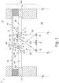
- Figure 1 shows an optical microphone assembly 2 comprising a substrate 4, a membrane 6, a light source 8 and two photo detectors 10.
- the substrate 4 comprises a first substrate portion 12 generally in the centre thereof and a second substrate portion 14 surrounding the first substrate portion.
- the substrate is manufactured from silicon.
- the first substrate portion 12 has a thickness of approximately 3 ⁇ m so that the silicon of the first substrate portion 12 is sufficiently thin to be substantially transparent to the wavelength of light provided by the light source 8, which is 850nm.
- a central region 13 of the first substrate portion 12 comprises two sub-portions 16, 18, each being provided with a respective diffractive optical element 20, 22.
- the diffractive optical elements 20, 22 comprise a plurality of reflective metal lines 24 deposited on the surface of the first substrate portion 12.
- the reflective lines are fabricated by depositing and patterning a metal layer, before performing a high-temperature LPCVD (low pressure chemical vapour deposition) processing step to deposit a highly tensile silicon nitride layer over the substrate.
- LPCVD low pressure chemical vapour deposition
- This approach would typically use a metal with a high melting point (such as tungsten) in order to withstand the LPCVD deposition step.
- a tensile film formed with a lower temperature process e.g. PECVD, plasma-enhanced chemical vapour deposition
- the LPCVD silicon nitride layer may provide two useful functions. It may function as an anti-reflection coating.
- the sub-portions 16, 18 have different thicknesses so as to introduce different phase delays to light passing therethrough. This provides two different working points with respect to which the membrane displacement is measured, which extends the working range of the optical microphone.
- this feature is not essential, and in variations on this embodiment and other embodiments, the first substrate portion 12 may have a uniform height and a single diffractive optical element.
- the light source 8 which in this example is a vertical-cavity surface-emitting laser (VCSEL), directs light 26 towards the first substrate portion 12.
- a first portion 28 of the light is reflected back from the diffractive optical elements 20, 22, and is incident on the detectors 10.
- a second portion 30 of the light is transmitted and diffracted by the diffractive optical elements 20, 22 and is incident on the membrane 6.
- the second portion 30 of light is reflected by the membrane 6, and propagates back through the first substrate portion 12 and is incident on the detectors 10.
- the first and second portions 28, 30 of light together create an interference pattern at the detectors 10.
- the interference pattern depends on the separation between the membrane 6 and the diffractive optical elements 20, 22.
- the measured intensity of light at the detectors 10 is used to determine the separation between the membrane 6 and the diffractive optical elements 20, 22, and thus to generate an output signal corresponding to the movement of the membrane 6.
- a plurality of holes 32 is provided in the first substrate portion 12.
- the plurality of holes 32 performs two functions. First, the holes 32 interrupt the optical paths taken by the light 26 and the first and second portions 28, 30 of light. The holes 32 therefore cause part of the light to be removed, such that it does not contribute to the interference pattern at the detectors.
- the light that is removed includes, for example, portions that contribute negatively to the optical signal strength and contrast.
- the holes 32 also serve as air passages such that an interstitial volume 34 between the substrate 4 and the membrane 6 is in fluid communication with an acoustic cavity 36 of the optical microphone assembly 2.
- the air passages provided by the holes 32 allow air that is displaced by movement of the membrane to flow out of the interstitial volume, thereby reducing acoustical squeeze-film resistance that may otherwise give rise to noise in the optical microphone output signal.
- the optical microphone assembly is shown as having a "top-port” configuration, i.e. wherein the acoustic cavity 36 is provided underneath the substrate 4, and the side of the membrane 6 facing away from the substrate 4 is in fluid communication with the exterior of the optical microphone 37.
- the optical microphone assembly may also be suitable for use in a "bottom-port” configuration, i.e. with an acoustic cavity enclosing a volume on the side of the membrane 6 that faces away from the substrate 4.
- the interstitial volume 34 would be in fluid communication with the exterior of the optical microphone assembly via the holes 32.
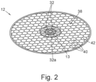
- the first substrate portion 12 comprises a perforated region 38, which surrounds a central region 13 of the first substrate portion 12. It can be seen that the holes 32 provided in the central region 13 of the first substrate portion 12 are arranged in concentric circles around a central hole 32a.
- the perforated region 38 comprises hexagonal perforations 40.
- the hexagonal perforations 40 are arranged in a hexagonal close-packed lattice arrangement.
- the perforations 40 occupy a large fraction of the area of the perforated region 38-in this example, the maximum area practicable while still maintaining sufficient structural integrity from the material 42 between the holes to support the central region 13 of the first substrate portion 12.
- the perforated region 38 provides air passages via which the interstitial volume 34 is in fluid communication with the acoustic cavity 36. This helps further to eliminate squeeze-film damping of the membrane and thereby to improve the performance of the optical microphone.
- the membrane 6 is provided with corrugations 44, which help to increase the membrane compliance and thus to increase the optical microphone sensitivity.
- the membrane 6 also comprises a central ventilation hole 46. This allows static equalization of pressure between the acoustic cavity and the microphone assembly exterior.
- the optical microphone assembly 2 also comprises a mounting structure 48, which comprises the second substrate portion 14. It can be seen that the mounting structure 48 is a composite structure comprising circumferential structures that support the membrane 6 and the first substrate portion 12. It can be seen that the mounting structure 48 is thicker than the first substrate portion 12. In this example, the mounting structure 48 is 400 ⁇ m thick. It will be appreciated that the dimensions of Figure 1 are not shown to scale. The thickness of the mounting structure 48 provides rigidity to reduce noise (e.g. thermo-mechanical noise) that may otherwise be caused by movement of thin first substrate portion 12.
- noise e.g. thermo-mechanical noise
- FIG 3 shows an alternative substrate 50 that may be used in optical microphone assemblies in accordance with the present invention, for example, in the optical microphone assembly 2 shown in Figure 1 .
- the substrate 50 comprises a first substrate portion 52 having a diffractive optical element (not shown) disposed on a central region 53 thereof.
- the central region 53 has holes 54 therethrough.
- the holes 54 are elongate and extend radially from a central point on the first substrate portion 52.
- the holes 54 perform an equivalent function to the holes 32 shown in Figures 1 and 2 .
- the substrate 50 comprises an apertured region 56.
- the apertured region 56 has three apertures 58 that extend fully through the substrate 50.
- the apertures 56 are arc-shaped sections surrounding the central region 53, such that the central region 53 has the form of central support platform supported by three radially extending beams 60.
- the apertures 50 perform a similar function to the perforations 40 shown in Figure 2 , i.e. putting an interstitial volume in fluid communication with an acoustic cavity.
- the substrate 50 also includes a second substrate portion 62, which is thicker than the first substrate portion 52 and forms part of a mounting structure when the substrate 50 is assembled in an optical microphone assembly.
- the beams 60 have the same thickness as the central region 53, although in variations on this and other embodiments, the beams 60 may be thicker than the central region 53, e.g. forming part of and having the same thickness as the second substrate portion 62.
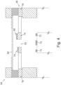
- Figure 4 shows a second embodiment of an optical microphone assembly 64.
- the optical microphone assembly 64 has equivalent features to the optical microphone assembly 2 shown in Figure 1 , i.e. a substrate 66, a membrane 68, a light source 70 and two detectors 72.
- the substrate 66 comprises a first substrate portion 74 and second substrate portion 76, the first substrate portion 74 having diffractive optical elements 78, 80 thereon.
- a single central hole 82 is provided instead of the plurality of holes 32.
- the hole 82 provides a similar function to the holes 32 of the embodiment of Figure 1 , except that due its different position, it removes a different portion of the light from the light source 8. The hole 82 therefore has a different impact on the interference pattern detected at detectors 72 compared with the arrangement shown in Figure 1 .
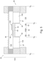
- Figure 5 shows an example of an optical microphone assembly 84 which is not part of the invention.
- the optical microphone assembly 84 has equivalent features to the optical microphone assembly 2 shown in Figures 1 and 4 , i.e. a substrate 86, a membrane 88, a light source 90 and two detectors 92.
- the substrate 86 comprises a first substrate portion 94 and second substrate portion 96, the first substrate portion 94 comprising a central region 95 having diffractive optical elements 98, 100 thereon. However, in this example, no holes are provided in the central region 95 of the first substrate portion 94.
- the first substrate portion 94 comprises only the central region 95
- the second substrate portion 96 (which is thicker than the first substrate portion 94) includes a peripheral region 97 which surrounds the central region 95 and has apertures 106 formed therein.
- An interstitial volume 102 is in fluid communication with an acoustic cavity 104 via the apertures 106.
- the apertures 106 have a similar form to the apertures 50 shown in and discussed with reference to Figure 3 , except that in this example the beams 60 form part of the second substrate portion 96, and so are thicker than the first substrate portion 94 (although this is not essential).
- a perforated region similar to perforated region 38 of Figures 1 and 2 may be provided instead of the apertures 106.
- the substrate 86 is made from silicon which, due to having a thickness of 3 ⁇ m, is substantially transparent to the light emitted by the light source 90, which in this example has a wavelength of 850nm, i.e. the substrate 86 is transparent by virtue of being sufficiently thin.
- silicon for the substrate 86 is advantageous because silicon is readily and precisely etched, allowing the apertures 106 (or perforations in variations on this example) to be etched in the substrate 86.
- the optical microphone assembly 84 comprises a mounting structure 108 which comprises the second substrate portion 96.
- the mounting structure 108 and the second substrate portion 96 are much thicker than the first substrate portion 94.
- the mounting structure (not shown to scale) is 400 ⁇ m thick.
- the mounting structure 108 and the second substrate portion 96 provide rigidity to reduce noise resulting from movement of the first substrate portion 94.
Landscapes
- Physics & Mathematics (AREA)
- General Physics & Mathematics (AREA)
- Engineering & Computer Science (AREA)
- Acoustics & Sound (AREA)
- Signal Processing (AREA)
- Electrostatic, Electromagnetic, Magneto- Strictive, And Variable-Resistance Transducers (AREA)
Description
- This invention relates generally to optical microphone assemblies and in particular to substrates for optical microphone assemblies.
- Microphones are used to convert sound waves into electrical signals, typically by measuring the displacement of a moveable member (e.g. a membrane) that vibrates in response to ambient acoustic vibrations. There are a number of ways of measuring the displacement of such a moveable member, including capacitive readout (commonly called condenser microphones) and electrostatic or electromagnetic readout mechanisms (e.g. dynamic microphones).
- An alternative way of reading out the position of a microphone membrane is optical interferometric read out. In typical examples of such systems, a diffraction grating is provided on a substrate adjacent to a membrane, and electromagnetic radiation is directed onto the diffraction grating. A first portion of the light is reflected back from the grating. A second portion is transmitted through the grating, which diffracts the radiation. The diffracted radiation impinges on the membrane, which reflects it onto the grating. The radiation passes through the grating and the two portions of light interfere to create an interference pattern that can be detected by a detector. The interference pattern has a shape (i.e. spatial distribution) matching the diffraction orders of the grating, but the light intensity directed into these diffraction orders depends on the relative phase of the two portions of light, and therefore on the distance between the grating and the membrane. The position (and therefore the movement) of the membrane can thus be determined from changes in the intensity of the light at the detector.
US 2006/0227845 andUS 7,440,117 describe displacement sensors that use optical interferometric read out. - Such microphones have a high signal to noise ratio (SNR) and high sensitivity. However, further improvements in the performance of such microphones are desirable.
- The invention provides an optical microphone assembly comprising:
- a substrate;
- an interferometic arrangement, the interferometric arrangement comprising a membrane and at least one diffractive optical element spaced from the membrane, wherein the at least one diffractive optical element comprises a plurality of lines formed in or disposed on a surface of the substrate, the plurality of lines being arranged in a first pattern; the optical microphone assembly further comprising:
- a light source arranged to provide light to said interferometric arrangement such that a first portion of said light propagates along a first optical path via said interferometric arrangement and a second portion of said light propagates along a second different optical path via said interferometric arrangement, thereby giving rise to an optical path difference between the first and second optical paths which depends on a distance between the membrane and the diffractive optical element; and
- at least one photo detector arranged to detect at least part of an interference pattern generated by said first and second portions of light dependent on said optical path difference;
- characterized in that the substrate comprises one or more holes extending fully through the substrate, the one or more holes being arranged in a second pattern that is different from the first pattern, wherein the one or more holes are positioned such that at least one of said first and second optical paths at least partly overlaps with the one or more holes.
- The invention extends to a method of manufacturing an optical microphone assembly, the optical microphone assembly comprising a substrate, a membrane, a light source and at least one photo detector, the method comprising:
- providing at least one diffractive optical element comprising a plurality of lines on a surface of the substrate by forming said plurality of lines in or on the surface, the plurality of lines being arranged in a first pattern;
- providing a membrane spaced from the diffractive optical element so as to form an interferometric arrangement;
- arranging a light source to provide light to said interferometric arrangement such that a first portion of said light propagates along a first optical path via said interferometric arrangement and a second portion of said light propagates along a second different optical path via said interferometric arrangement, thereby giving rise to an optical path difference between the first and second optical paths which depends on a distance between the membrane and the diffractive optical element; and
- arranging at least one photo detector to detect at least part of an interference pattern generated by said first and second portions of light dependent on said optical path difference;
- characterized in that the method comprises forming one or more holes in the substrate, the one or more holes extending fully through the substrate and being arranged in a second pattern that is different from the first pattern, wherein the one or more holes are positioned such that at least one of said first and second optical paths at least partly overlaps with the one or more holes.
- The Applicant has appreciated that providing one or more holes in the substrate as described above can provide certain advantages over microphone assemblies of the prior art. As the hole(s) at least partly overlap with the optical path taken by the light through the interferometric arrangement, the hole(s) may affect the light that is transmitted by or reflected from the substrate. For example, the hole(s) may remove some of the light that would otherwise have contributed to the diffraction pattern created by the diffractive optical element. It is therefore to be understood that when it is said that at least one of said first and second optical paths at least partly overlaps with the one or more holes, this refers to the optical path(s) that would have been taken by the first and/or second portions of light from the light source to the detector(s) if the hole(s) were not present. The holes may help to improve the performance of the optical microphone assembly, for example, by removing parts of the light that contribute negatively to the optical signal strength and/or contrast.
- Another way that the hole(s) may help to improve the performance of the optical microphone assembly is by changing its acoustic properties. For example, the hole(s) may help to reduce acoustical squeeze-film resistance between the membrane and the substrate that may otherwise give rise to noise in the optical microphone output signal. The hole(s) may also help to reduce squeeze-film noise displacement of the substrate, thereby reducing the total measured thermo-mechanical noise in the optical microphone.
- Although the hole(s) may affect the light that is transmitted by or reflected from the substrate, it is to be understood that the holes do not form part of the diffractive optical element. In particular, the diffractive optical element is not defined by the hole(s), i.e. the diffractive optical element is not formed by forming the hole(s) in the substrate. The diffractive optical element is diffractive due to comprising lines (e.g. grating lines) arranged in the first pattern. The hole(s) may be described as being uncorrelated with the diffraction pattern produced by the lines of the diffractive optical element. The hole(s) may overlap with the at least one diffractive optical element. For example, in a set of embodiments, the first and second patterns have respective first and second envelopes, wherein the first and second envelopes overlap. At least one, at least some or all of the hole(s) may be positioned within the first envelope.
- As noted above, the presence of the hole(s) may advantageously improve the acoustic and/or optical properties of the optical microphone (e.g. by reducing squeeze film resistance and/or removing negative contributions to the optical signal strength/contrast). While the presence of one or more holes may provide such advantages, the benefit may be improved by selecting (e.g. optimising) the properties of the holes. For example, the size, shape, arrangement and/or other properties of the holes may be selected to increase the associated benefits.
- The length scale of the one or more holes (e.g. a width or length of the one or more holes) would typically be larger than an average spacing between the lines (e.g. the distance between adjacent lines). For example, the length scale of the one or more holes may be at least 3 times larger, at least 5 times larger, at least 10 times larger, at least 15 times larger or at least 20 times larger than the average spacing between the lines. In some embodiments, a small number of large holes is provided. For example, the number of holes may be between 1 and 8, between 2 and 6 or between 3 and 5.
- When it is said that the holes are arranged in a pattern (i.e. the second pattern), it is to be understood that the term "pattern" does not necessarily imply any symmetry or repetition in the arrangement of holes, although the pattern may have symmetry, e.g. rotational, reflectional and/or translational symmetry. The second pattern may comprise one or more of: a single central hole; radially extending elongate holes, e.g. 2, 3, 4, 5, 6, 7, 8, or more than 8 radially extending elongate holes; radially extending lines of holes, e.g. in which a line of two or more holes extends from a centre point or a centre hole; concentric circles of holes, e.g. surrounding a central hole. Other patterns are possible. The hole(s) may be circular.
- When it is said that hole(s) extend "fully through" the substrate, it is to be understood that this means that the hole(s) extend through the substrate so as to form an air passage connecting one side of the substrate to the other, e.g. so that regions on either side of the substrate are in fluid communication through the hole(s). The method of manufacture may comprise etching the one or more holes in the substrate.
- The lines of the diffractive optical element(s) may be etched into or deposited on the substrate. Where they are etched, they are preferably non-perforating, i.e. they preferably do not extend fully through the substrate. The lines may be deposited metal lines.
- The lines may form a diffraction grating. The lines may be straight, although this is not essential and in some embodiments the lines are curved. For example, the diffractive optical element may be a Fresnel lens.
- The Applicant has appreciated that certain advantages may be obtained if the substrate or a portion thereof bearing the diffractive optical element is thin. In a set of embodiments, the substrate comprises a first substrate portion, wherein the at least one diffractive optical element is disposed on or formed in the first substrate portion. The substrate or the first substrate portion may have a thickness of thickness of 1µm to 20µm, preferably 2µm to 10µm, more preferably 3µm to 5µm. In a set of embodiments, one or both of the first and second portions of light impinges on the first substrate portion. In a set of embodiments, at least one of the first and second light paths passes through the first substrate portion.
- Having a thin substrate may provide advantages associated with optical transparency, acoustic performance and manufacturability.
- Preferably the substrate or the first substrate portion is substantially transparent at the wavelength of the light provided by the light source, e.g. such that the majority of light that impinges on the substrate or the first substrate portion is transmitted after two passes through the substrate (i.e. after entering the substrate, being reflected from a surface of the substrate and passing back through the substrate again). For example, at least 80%, at least 90% or at least 95% of the light may be transmitted after two passes through the substrate. The transparency of the substrate may be achieved by virtue of the substrate of the first substrate portion being sufficiently thin for the light to be transmitted, e.g. the thickness of the substrate or the first substrate portion may be selected to provide a transparency according to the percentages specified above. The substrate or part thereof (e.g. the first substrate portion) may be provided with an anti-reflection coating on one or both sides thereof. Reflections from the substrate surface may thereby be reduced.
- The transparency of the substrate or first substrate portion may be wavelength-dependent, and the thickness required to achieve a particular transparency may depend on the material the substrate is made from. Accordingly, the thickness of the substrate or first substrate portion may selected to achieve a particular transparency for the wavelength of the light provided by the light source for a given substrate material. The wavelength of the light provided by the light source may be in the range 800nm to 1000nm, e.g. 850nm or 940nm. If the wavelength is 850nm, the substrate or first substrate portion thickness may be about 3µm if the substrate is made from silicon. At other wavelengths and/or for other materials, the thickness may be less than or greater than 3µm. For example, if the wavelength of the light is 940nm, the substrate or first substrate portion thickness may be about 10µm if the substrate material is silicon.
- The use of a thin substrate may advantageously allow the use of substrate materials that would otherwise be too opaque to be used. These materials may provide advantages over conventional materials (e.g. glass) that are transparent even at greater thicknesses, e.g. such as improved manufacturability. For example, the substrate may be made from silicon. Silicon is particularly advantageous as it can be readily and precisely etched to provide the required form of the substrate, e.g. including holes, apertures, and/or perforations as discussed elsewhere herein. Where the substrate (or the first substrate portion) is made from silicon, preferably the silicon is monocrystalline silicon. The silicon may be undoped or doped at a low level such that a suitable substrate transparency (as discussed above) is achieved.
- The substrate and/or the first substrate portion may comprise a layered structure (e.g. a sandwich of different materials, e.g including a silicon layer). The layered structure may consist of two, three or more than three layers, e.g. a first layer with a thin film layer on one or both sides. For example, the layered structure may comprise or consist of mono-crystalline silicon (e.g. a 3µm-thick layer) with a thin film on one or both sides. The thin film may comprise an anti-reflection coating. The thin film may have a high tensile stress (e.g. 1GPa or higher than 1GPa), e.g. in order to stiffen the substrate or the first substrate portion.
- A thin substrate may also improve the acoustic properties of the optical microphone assembly. For example, holes with a lower aspect ratio (i.e. formed in a thinner substrate) may provide a greater improvement of the acoustic properties of the optical microphone compared with holes of the same shape, size and pattern in a thicker substrate. Holes formed in a thinner substrate may be more easily manufactured.
- The optical microphone assembly may comprise more than one diffractive optical element. Each diffractive optical element may introduce a different relative phase delay to light transmitted or reflected by the diffractive optical element. For example, the substrate (or first substrate portion) may have regions of different thickness such that each diffractive optical element has a different height. The displacement of the membrane may thus be measured with respect to a different working point for each diffractive optical element, thereby extending the working range of the optical microphone.
- The substrate may comprise a second substrate portion, e.g. surrounding the first substrate portion. The second substrate portion may be thicker than the first substrate portion. This may help to provide rigidity/stiffness for the substrate as a whole, and thus for the first substrate portion. Increased rigidity/stiffness may help to reduce noise, for example, by reducing movement of the substrate (or first substrate portion) which would otherwise contribute to the noise floor.
- The substrate may be integrally formed from a single piece of material, such that the first and second substrate portions are made from the same material. For example, the first substrate portion may be a thinned region of the single piece. The method of manufacture may comprise etching a region of the substrate so as to provide a first substrate portion that is thinner than a second substrate potion, e.g. wherein the second substrate portion surrounds the first substrate portion.
- The first and second substrate portions may comprise two distinct pieces that are attached together. The first substrate portion may be formed from silicon.
- The optical microphone assembly may be arranged such that the first and second portions of light do not impinge on and/or do not pass through the second substrate portion. The second substrate portion may be substantially opaque at the wavelength of light provided by the light source. For example, the second substrate portion may be substantially opaque due to its thickness, e.g. if it is made from the same material as the first substrate portion, due its material or because a covering is provided thereon. As discussed below, the second substrate portion may include apertures or perforations. Accordingly, when it is said that the second substrate portion may be substantially opaque, it is to be understood that this means that the parts of the second substrate portion other than any apertures or perforations are opaque.
- The optical microphone assembly may comprise an interstitial volume, wherein the substrate and membrane together define the interstitial volume therebetween. The optical microphone assembly may comprise an acoustic cavity, wherein a first side of the membrane is in fluid communication with the acoustic cavity and a second side of the membrane is in fluid communication with the exterior of the optical microphone assembly.
- In a set of embodiments, the substrate comprises an apertured region, the apertured region comprising one or more apertures extending fully through the substrate. For example, the substrate may comprise a plurality of apertures surrounding a central support portion of the substrate, the central support portion comprising the at least one diffractive optical element. The apertured region may be provided in the first substrate portion or in the second substrate portion. The apertures may provide a passage for air connecting the interstitial volume either with the acoustic cavity of the optical microphone assembly or with the exterior of the optical microphone assembly so that these regions are in fluid communication.
- Additionally or more typically alternatively, the substrate may comprise a perforated region, the perforated region comprising perforations extending fully through the substrate. The perforated region may be provided in the first substrate portion or in the second substrate portion. The perforated region may provide a passage for air connecting the interstitial volume either with the acoustic cavity of the optical microphone assembly or with the exterior of the optical microphone assembly so that these regions are in fluid communication. This may help to improve the performance of the optical microphone assembly by reducing the acoustic resistance between the membrane and the substrate. The perforated region may be highly perforated, e.g. such that the total area of the perforations comprises greater than 50%, greater than 80%, greater than 90% or greater than 95% of the perforated region. Additionally or alternatively, the perforations may have tessellating shapes, e.g. squares, hexagons, triangles, rectangles. The perforations may be in a lattice arrangement, e.g. square lattice, hexagonal close packed. The perforated region of the second substrate portion may be maximally perforated. In this context, maximally perforated means that the total area of the perforations is maximised as much as practicable while maintaining sufficient structural integrity of the second substrate portion to support the first substrate portion. Maximising the degree of perforation in this way can help to minimise the acoustic resistance between the membrane and the substrate.
- It is to be appreciated that the apertures and perforations, where provided, are different from the holes in the first substrate portion and are not for providing the function of removing parts of the diffracted/reflected light. Accordingly, where the perforated region and/or the apertured region is provided in the first substrate portion, neither the apertures nor the perforations overlap with the first or second light path.
- Apertures and perforations as described in this context differ in that perforations are typically smaller and more numerous than apertures.
- The second substrate portion may be made from a different material from the first substrate portion. Where the perforated region and/or the apertured region is formed in the first substrate portion, the perforated region and/or the apertured region may be made from a different material from the rest of the first substrate potion. The second substrate portion, the perforated region and/or the apertured region may be made from a material that does not transmit light at the wavelength of the light from the light source, e.g. polysilicon. The method of manufacture may comprise etching perforations in the substrate to form the perforated region.
- The shape, size and/or arrangement of the apertures and/or perforations may be selected, e.g. optimized, to increase fluid communication between the interstitial volume and the acoustic cavity or optical microphone assembly exterior, e.g. to reduce or minimise acoustic resistance between the membrane and the substrate.
- The optical microphone assembly may comprise a mount structure which supports the membrane and substrate. The mount structure may be a composite structure and may comprise the second substrate portion. The thickness of mount structure may be less than 1mm, e.g. less than 500µm, e.g. less than 400µm.
- The membrane may be made from any suitable material, for example, silicon nitride. The membrane may be provided with corrugations, e.g. to increase membrane compliance, although corrugations are not essential. The membrane may be provided with a ventilation hole, although this is not essential. The ventilation hole may allow static equalization of pressure between the acoustic cavity and the microphone assembly exterior.
- As discussed above, providing a relatively thin first substrate portion and a thicker second substrate portion, e.g. surrounding the first substrate portion, provides certain advantages. Using a thin first substrate portion opens up the possibility of manufacturing the substrate from materials that would otherwise be too opaque to use, while providing a thicker second substrate portion can provide rigidity to mitigate the effects of noise.
- Certain preferred embodiments will now be described, by way of example only, with reference to the accompanying drawings, in which:
-
Figure 1 shows a cross-sectional view of a first embodiment of an optical microphone assembly in accordance with the present invention; -
Figure 2 shows a perspective view of part of the substrate of the optical microphone assembly ofFigure 1 ; -
Figure 3 shows an alternative substrate for use in optical microphone assemblies in accordance with the present invention; -
Figure 4 shows a cross-sectional view of a second embodiment of an optical microphone assembly in accordance with the present invention; and -
Figure 5 shows a cross-sectional view of an example of an optical microphone assembly which is not part of the present invention. -
Figure 1 shows anoptical microphone assembly 2 comprising a substrate 4, a membrane 6, a light source 8 and twophoto detectors 10. The substrate 4 comprises afirst substrate portion 12 generally in the centre thereof and asecond substrate portion 14 surrounding the first substrate portion. The substrate is manufactured from silicon. Thefirst substrate portion 12 has a thickness of approximately 3µm so that the silicon of thefirst substrate portion 12 is sufficiently thin to be substantially transparent to the wavelength of light provided by the light source 8, which is 850nm. In this example, acentral region 13 of thefirst substrate portion 12 comprises two sub-portions 16, 18, each being provided with a respective diffractiveoptical element optical elements reflective metal lines 24 deposited on the surface of thefirst substrate portion 12. In this example, the reflective lines are fabricated by depositing and patterning a metal layer, before performing a high-temperature LPCVD (low pressure chemical vapour deposition) processing step to deposit a highly tensile silicon nitride layer over the substrate. This approach would typically use a metal with a high melting point (such as tungsten) in order to withstand the LPCVD deposition step. Alternatively, a tensile film formed with a lower temperature process (e.g. PECVD, plasma-enhanced chemical vapour deposition) may be employed. The LPCVD silicon nitride layer may provide two useful functions. It may function as an anti-reflection coating. It may also help to stiffen the substrate (or first substrate portion) due to its high tensile stress, which may advantageously reduce noise from movement of the substrate (or first substrate portion). However, neither the LPCVD silicon nitride layer nor the PECVD tensile film is essential. - The sub-portions 16, 18 have different thicknesses so as to introduce different phase delays to light passing therethrough. This provides two different working points with respect to which the membrane displacement is measured, which extends the working range of the optical microphone. However, this feature is not essential, and in variations on this embodiment and other embodiments, the
first substrate portion 12 may have a uniform height and a single diffractive optical element. - The light source 8, which in this example is a vertical-cavity surface-emitting laser (VCSEL), directs light 26 towards the
first substrate portion 12. Afirst portion 28 of the light is reflected back from the diffractiveoptical elements detectors 10. Asecond portion 30 of the light is transmitted and diffracted by the diffractiveoptical elements second portion 30 of light is reflected by the membrane 6, and propagates back through thefirst substrate portion 12 and is incident on thedetectors 10. The first andsecond portions detectors 10. The interference pattern depends on the separation between the membrane 6 and the diffractiveoptical elements detectors 10 is used to determine the separation between the membrane 6 and the diffractiveoptical elements - A plurality of
holes 32 is provided in thefirst substrate portion 12. The plurality ofholes 32 performs two functions. First, theholes 32 interrupt the optical paths taken by the light 26 and the first andsecond portions holes 32 therefore cause part of the light to be removed, such that it does not contribute to the interference pattern at the detectors. The light that is removed includes, for example, portions that contribute negatively to the optical signal strength and contrast. - The
holes 32 also serve as air passages such that aninterstitial volume 34 between the substrate 4 and the membrane 6 is in fluid communication with anacoustic cavity 36 of theoptical microphone assembly 2. The air passages provided by theholes 32 allow air that is displaced by movement of the membrane to flow out of the interstitial volume, thereby reducing acoustical squeeze-film resistance that may otherwise give rise to noise in the optical microphone output signal. - In this example, the optical microphone assembly is shown as having a "top-port" configuration, i.e. wherein the
acoustic cavity 36 is provided underneath the substrate 4, and the side of the membrane 6 facing away from the substrate 4 is in fluid communication with the exterior of theoptical microphone 37. However, the optical microphone assembly may also be suitable for use in a "bottom-port" configuration, i.e. with an acoustic cavity enclosing a volume on the side of the membrane 6 that faces away from the substrate 4. In such arrangements, theinterstitial volume 34 would be in fluid communication with the exterior of the optical microphone assembly via theholes 32. - As shown in perspective view in
Figure 2 , thefirst substrate portion 12 comprises aperforated region 38, which surrounds acentral region 13 of thefirst substrate portion 12. It can be seen that theholes 32 provided in thecentral region 13 of thefirst substrate portion 12 are arranged in concentric circles around acentral hole 32a. Theperforated region 38 compriseshexagonal perforations 40. Thehexagonal perforations 40 are arranged in a hexagonal close-packed lattice arrangement. Theperforations 40 occupy a large fraction of the area of the perforated region 38-in this example, the maximum area practicable while still maintaining sufficient structural integrity from the material 42 between the holes to support thecentral region 13 of thefirst substrate portion 12. Theperforated region 38 provides air passages via which theinterstitial volume 34 is in fluid communication with theacoustic cavity 36. This helps further to eliminate squeeze-film damping of the membrane and thereby to improve the performance of the optical microphone. - Returning to
Figure 1 , it can be seen that the membrane 6 is provided withcorrugations 44, which help to increase the membrane compliance and thus to increase the optical microphone sensitivity. The membrane 6 also comprises acentral ventilation hole 46. This allows static equalization of pressure between the acoustic cavity and the microphone assembly exterior. - The
optical microphone assembly 2 also comprises a mountingstructure 48, which comprises thesecond substrate portion 14. It can be seen that the mountingstructure 48 is a composite structure comprising circumferential structures that support the membrane 6 and thefirst substrate portion 12. It can be seen that the mountingstructure 48 is thicker than thefirst substrate portion 12. In this example, the mountingstructure 48 is 400µm thick. It will be appreciated that the dimensions ofFigure 1 are not shown to scale. The thickness of the mountingstructure 48 provides rigidity to reduce noise (e.g. thermo-mechanical noise) that may otherwise be caused by movement of thinfirst substrate portion 12. -
Figure 3 shows analternative substrate 50 that may be used in optical microphone assemblies in accordance with the present invention, for example, in theoptical microphone assembly 2 shown inFigure 1 . Thesubstrate 50 comprises afirst substrate portion 52 having a diffractive optical element (not shown) disposed on acentral region 53 thereof. Thecentral region 53 hasholes 54 therethrough. Theholes 54 are elongate and extend radially from a central point on thefirst substrate portion 52. Theholes 54 perform an equivalent function to theholes 32 shown inFigures 1 and2 . - The
substrate 50 comprises anapertured region 56. Theapertured region 56 has threeapertures 58 that extend fully through thesubstrate 50. Theapertures 56 are arc-shaped sections surrounding thecentral region 53, such that thecentral region 53 has the form of central support platform supported by three radially extending beams 60. In an optical microphone assembly, e.g. such as theassembly 2 inFigure 1 , theapertures 50 perform a similar function to theperforations 40 shown inFigure 2 , i.e. putting an interstitial volume in fluid communication with an acoustic cavity. Thesubstrate 50 also includes asecond substrate portion 62, which is thicker than thefirst substrate portion 52 and forms part of a mounting structure when thesubstrate 50 is assembled in an optical microphone assembly. In this example, thebeams 60 have the same thickness as thecentral region 53, although in variations on this and other embodiments, thebeams 60 may be thicker than thecentral region 53, e.g. forming part of and having the same thickness as thesecond substrate portion 62. -
Figure 4 shows a second embodiment of anoptical microphone assembly 64. Theoptical microphone assembly 64 has equivalent features to theoptical microphone assembly 2 shown inFigure 1 , i.e. a substrate 66, amembrane 68, alight source 70 and twodetectors 72. The substrate 66 comprises afirst substrate portion 74 andsecond substrate portion 76, thefirst substrate portion 74 having diffractiveoptical elements holes 32, a singlecentral hole 82 is provided. Thehole 82 provides a similar function to theholes 32 of the embodiment ofFigure 1 , except that due its different position, it removes a different portion of the light from the light source 8. Thehole 82 therefore has a different impact on the interference pattern detected atdetectors 72 compared with the arrangement shown inFigure 1 . -
Figure 5 shows an example of anoptical microphone assembly 84 which is not part of the invention. Theoptical microphone assembly 84 has equivalent features to theoptical microphone assembly 2 shown inFigures 1 and4 , i.e. asubstrate 86, amembrane 88, alight source 90 and twodetectors 92. Thesubstrate 86 comprises afirst substrate portion 94 andsecond substrate portion 96, thefirst substrate portion 94 comprising acentral region 95 having diffractiveoptical elements central region 95 of thefirst substrate portion 94. In addition, thefirst substrate portion 94 comprises only thecentral region 95, and the second substrate portion 96 (which is thicker than the first substrate portion 94) includes aperipheral region 97 which surrounds thecentral region 95 and hasapertures 106 formed therein. Aninterstitial volume 102 is in fluid communication with anacoustic cavity 104 via theapertures 106. Theapertures 106 have a similar form to theapertures 50 shown in and discussed with reference toFigure 3 , except that in this example thebeams 60 form part of thesecond substrate portion 96, and so are thicker than the first substrate portion 94 (although this is not essential). In variations on this example, a perforated region similar toperforated region 38 ofFigures 1 and2 may be provided instead of theapertures 106. Thesubstrate 86 is made from silicon which, due to having a thickness of 3µm, is substantially transparent to the light emitted by thelight source 90, which in this example has a wavelength of 850nm, i.e. thesubstrate 86 is transparent by virtue of being sufficiently thin. Using silicon for thesubstrate 86 is advantageous because silicon is readily and precisely etched, allowing the apertures 106 (or perforations in variations on this example) to be etched in thesubstrate 86. - The
optical microphone assembly 84 comprises a mountingstructure 108 which comprises thesecond substrate portion 96. The mountingstructure 108 and thesecond substrate portion 96 are much thicker than thefirst substrate portion 94. In this example, the mounting structure (not shown to scale) is 400µm thick. The mountingstructure 108 and thesecond substrate portion 96 provide rigidity to reduce noise resulting from movement of thefirst substrate portion 94. - It will be appreciated that only some embodiments of the present invention have been described above, and that other embodiments and variations on the above-described embodiments are possible within the scope of the invention. The scope of the invention is defined by the appended claims.
Claims (15)
- An optical microphone assembly (2; 64) comprising:a substrate (4; 50; 66);an interferometic arrangement, the interferometric arrangement comprising a membrane (6; 68) and at least one diffractive optical element (20, 22; 78, 80) spaced from the membrane (6; 68), wherein the at least one diffractive optical element (20, 22; 78, 80) comprises a plurality of lines (24) formed in or disposed on a surface of the substrate (4; 50; 66), the plurality of lines (24) being arranged in a first pattern; the optical microphone assembly (2; 64) further comprising:a light source (8; 70) arranged to provide light to said interferometric arrangement such that a first portion (28) of said light propagates along a first optical path via said interferometric arrangement and a second portion (30) of said light propagates along a second different optical path via said interferometric arrangement, thereby giving rise to an optical path difference between the first and second optical paths which depends on a distance between the membrane (6; 68) and the diffractive optical element (20, 22; 78, 80); andat least one photo detector (10; 72) arranged to detect at least part of an interference pattern generated by said first and second portions of light (28, 30) dependent on said optical path difference;characterized in that the substrate (4; 50; 66) comprises one or more holes (32; 54; 82) extending fully through the substrate (4; 50; 66), the one or more holes (32; 54; 82) being arranged in a second pattern that is different from the first pattern, wherein the one or more holes (32; 54; 82) are positioned such that at least one of said first and second optical paths at least partly overlaps with the one or more holes (32; 54; 82).
- The optical microphone assembly (2; 64) of claim 1, wherein the first and second patterns have respective first and second envelopes, wherein the first and second envelopes overlap.
- The optical microphone assembly (2; 64) of claim 2, wherein at least one, at least some or all of the hole(s) (32; 54; 82) are positioned within the first envelope.
- The optical microphone assembly (2; 64) of claim 1, 2 or 3, wherein the length scale of the one or more holes (32; 54; 82) is at least 3 times larger, at least 5 times larger, at least 10 times larger, at least 15 times larger or at least 20 times larger than an average spacing between the lines (24).
- The optical microphone assembly (2; 64) of any preceding claim, wherein the number of holes (32; 54; 82) is between 1 and 8, between 2 and 6 or between 3 and 5.
- The optical microphone assembly (2; 64) of any preceding claim, wherein the second pattern comprises one or more of: a single central hole; radially extending elongate holes; radially extending lines of holes; and concentric circles of holes.
- The optical microphone assembly (2; 64) of any preceding claim, wherein the lines (24) of the diffractive optical element(s) (20, 22; 78, 80) are etched into or deposited on the substrate (4; 50; 66).
- The optical microphone assembly (2; 64) of any preceding claim, wherein the substrate (4; 50; 66) comprises a first substrate portion (12; 52; 74), and the at least one diffractive optical element (20, 22; 78, 80) is disposed on or formed in the first substrate portion (12; 52; 74).
- The optical microphone assembly (2; 64) of any preceding claim, wherein the substrate (4; 50; 66) or the first substrate portion (12; 52; 74) has a thickness of thickness of 1µm to 20µm, preferably 2µm to 10µm, more preferably 3µm to 5µm.
- The optical microphone assembly (2; 64) of any preceding claim, wherein the substrate (4; 50; 66) or the first substrate portion (12; 52; 74) is substantially transparent at the wavelength of the light provided by the light source (8; 70).
- The optical microphone assembly (2; 64) of any preceding claim, wherein the substrate (4; 50; 66) or the first substrate portion (12; 52; 74) comprises a layered structure, wherein the layered structure consists of two, three or more than three layers.
- The optical microphone assembly (2; 64) of claim 11, wherein the layered structure comprises a mono-crystalline silicon layer with a thin film on one or both sides, wherein the thin film provides an anti-reflection coating and/or wherein the thin film has a tensile stress of at least 1GPa.
- The optical microphone assembly (2; 64) of any preceding claim, wherein the substrate (4; 50; 66) comprises a second substrate portion (14; 62; 76) surrounding a or the first substrate portion (12; 52; 74), wherein the second substrate portion (14; 62; 76) is thicker than the first substrate portion (12; 52; 74), wherein the optical microphone assembly (2; 64) is arranged such that the first and second portions of light (28, 30) do not impinge on and/or do not pass through the second substrate portion (14; 62; 76).
- The optical microphone assembly (2; 64) of any preceding claim, further comprising an interstitial volume (34) wherein the substrate (4; 50; 66) and membrane (6; 68) together define the interstitial volume (34) therebetween, and wherein the optical microphone assembly (2; 64) further comprises an acoustic cavity (36), wherein a first side of the membrane (6; 68) is in fluid communication with the acoustic cavity (36) and a second side of the membrane (6; 68) is in fluid communication with the exterior (37) of the optical microphone assembly (2; 64); andi) wherein the substrate (4; 50; 66) comprises an apertured region (56) comprising one or more apertures (58) extending fully through the substrate (4; 50; 66), wherein the apertures (58) provide a passage for air connecting the interstitial volume (34) either with the acoustic cavity (36) of the optical microphone assembly (2; 64) or with the exterior (37) of the optical microphone assembly (2; 64); orii) wherein the substrate (4; 50; 66) comprises a perforated region (38) comprising perforations (40) extending fully through the substrate (4; 50; 66), wherein the perforated region (38) provides a passage for air connecting the interstitial volume (34) either with the acoustic cavity (36) of the optical microphone assembly (2; 64) or with the exterior (37) of the optical microphone assembly (2; 64).
- A method of manufacturing an optical microphone assembly (2; 64), the optical microphone assembly (2; 64) comprising a substrate (4; 50; 66), a membrane (6; 68), a light source (8; 70) and at least one photo detector (10; 72), the method comprising:providing at least one diffractive optical element (20, 22; 78, 80) comprising a plurality of lines (24) on a surface of the substrate (4; 50; 66) by forming said plurality of lines (24) in or on the surface, the plurality of lines (24) being arranged in a first pattern;providing a membrane (6; 68) spaced from the diffractive optical element (20, 22; 78, 80) so as to form an interferometric arrangement;arranging a light source (8; 70) to provide light to said interferometric arrangement such that a first portion (28) of said light propagates along a first optical path via said interferometric arrangement and a second portion (30) of said light propagates along a second different optical path via said interferometric arrangement, thereby giving rise to an optical path difference between the first and second optical paths which depends on a distance between the membrane (6; 68) and the diffractive optical element (20, 22; 78, 80); andarranging at least one photo detector (10; 72) to detect at least part of an interference pattern generated by said first and second portions of light (28, 30) dependent on said optical path difference;characterized in that the method comprises forming one or more holes (32; 54; 82) in the substrate (4; 50; 66), the one or more holes (32; 54; 82) extending fully through the substrate (4; 50; 66) and being arranged in a second pattern that is different from the first pattern, wherein the one or more holes (32; 54; 82) are positioned such that at least one of said first and second optical paths at least partly overlaps with the one or more holes (32; 54; 82).
Applications Claiming Priority (2)
| Application Number | Priority Date | Filing Date | Title |
|---|---|---|---|
| GBGB1916380.7A GB201916380D0 (en) | 2019-11-11 | 2019-11-11 | Optical microphone substrate |
| PCT/GB2020/052867 WO2021094747A1 (en) | 2019-11-11 | 2020-11-11 | Optical microphone substrate |
Publications (2)
| Publication Number | Publication Date |
|---|---|
| EP4059231A1 EP4059231A1 (en) | 2022-09-21 |
| EP4059231B1 true EP4059231B1 (en) | 2024-09-04 |
Family
ID=69062268
Family Applications (1)
| Application Number | Title | Priority Date | Filing Date |
|---|---|---|---|
| EP20811046.0A Active EP4059231B1 (en) | 2019-11-11 | 2020-11-11 | Optical microphone substrate |
Country Status (5)
| Country | Link |
|---|---|
| US (2) | US12069432B2 (en) |
| EP (1) | EP4059231B1 (en) |
| JP (1) | JP2023500959A (en) |
| GB (1) | GB201916380D0 (en) |
| WO (1) | WO2021094747A1 (en) |
Families Citing this family (4)
| Publication number | Priority date | Publication date | Assignee | Title |
|---|---|---|---|---|
| CN112449295A (en) | 2019-08-30 | 2021-03-05 | 华为技术有限公司 | Microphone chip, microphone and terminal equipment |
| GB202019714D0 (en) * | 2020-12-14 | 2021-01-27 | Sensibel As | Optical displacement sensor |
| US11917366B1 (en) * | 2022-09-26 | 2024-02-27 | Aac Acoustic Technologies (Shenzhen) Co., Ltd. | MEMS optical microphone |
| CN115802261A (en) * | 2022-12-19 | 2023-03-14 | 电子科技大学 | A diffraction grating, its preparation method and an optical microphone |
Family Cites Families (6)
| Publication number | Priority date | Publication date | Assignee | Title |
|---|---|---|---|---|
| KR100437142B1 (en) | 2001-12-07 | 2004-06-25 | 에피밸리 주식회사 | Optical microphone |
| US7440117B2 (en) | 2002-03-29 | 2008-10-21 | Georgia Tech Research Corp. | Highly-sensitive displacement-measuring optical device |
| US7485847B2 (en) * | 2004-12-08 | 2009-02-03 | Georgia Tech Research Corporation | Displacement sensor employing discrete light pulse detection |
| US8488973B2 (en) | 2010-02-11 | 2013-07-16 | Silicon Audio, Inc. | Signal processing within an optical microphone |
| US9973860B2 (en) * | 2016-04-05 | 2018-05-15 | Infineon Technologies Ag | System and method for an optical MEMS transducer |
| GB201807889D0 (en) | 2018-05-15 | 2018-06-27 | Sintef Tto As | Microphone housing |
-
2019
- 2019-11-11 GB GBGB1916380.7A patent/GB201916380D0/en not_active Ceased
-
2020
- 2020-11-11 JP JP2022526741A patent/JP2023500959A/en active Pending
- 2020-11-11 WO PCT/GB2020/052867 patent/WO2021094747A1/en not_active Ceased
- 2020-11-11 EP EP20811046.0A patent/EP4059231B1/en active Active
- 2020-11-11 US US17/775,699 patent/US12069432B2/en active Active
-
2024
- 2024-07-16 US US18/774,567 patent/US12328548B2/en active Active
Also Published As
| Publication number | Publication date |
|---|---|
| US20220408198A1 (en) | 2022-12-22 |
| US12328548B2 (en) | 2025-06-10 |
| JP2023500959A (en) | 2023-01-11 |
| US20240373171A1 (en) | 2024-11-07 |
| GB201916380D0 (en) | 2019-12-25 |
| US12069432B2 (en) | 2024-08-20 |
| WO2021094747A1 (en) | 2021-05-20 |
| EP4059231A1 (en) | 2022-09-21 |
Similar Documents
| Publication | Publication Date | Title |
|---|---|---|
| US12328548B2 (en) | Optical microphone substrate | |
| US11240607B2 (en) | Optical microphone assembly | |
| EP3942263B1 (en) | Optical microphone assembly | |
| US20110038492A1 (en) | Optical sensing in a directional mems microphone | |
| JP5739224B2 (en) | Optical component manufacturing method and optical component | |
| CN109060106B (en) | Dual-cavity combined photointerferometric acoustic sensor probe and its sensing system | |
| US20210258700A1 (en) | Optical microphone | |
| US20180208454A1 (en) | Flexible membrane | |
| US9939565B2 (en) | Reflective element for fiber optic sensor | |
| US12041415B2 (en) | Apparatus for sound detection, sound localization and beam forming and method of producing such apparatus | |
| EP4477989A2 (en) | Optical displacement sensor | |
| CN114902696B (en) | Microstructure and method for manufacturing microstructure | |
| JP2023123198A (en) | force sensor | |
| CN219087309U (en) | Integrated optical fiber MEMS microphone probe and optical fiber MEMS microphone | |
| US20240329077A1 (en) | Optical displacement sensors | |
| CN111464927A (en) | Optical fiber microphone and sensitive structure and preparation method thereof |
Legal Events
| Date | Code | Title | Description |
|---|---|---|---|
| STAA | Information on the status of an ep patent application or granted ep patent |
Free format text: STATUS: UNKNOWN |
|
| STAA | Information on the status of an ep patent application or granted ep patent |
Free format text: STATUS: THE INTERNATIONAL PUBLICATION HAS BEEN MADE |
|
| PUAI | Public reference made under article 153(3) epc to a published international application that has entered the european phase |
Free format text: ORIGINAL CODE: 0009012 |
|
| STAA | Information on the status of an ep patent application or granted ep patent |
Free format text: STATUS: REQUEST FOR EXAMINATION WAS MADE |
|
| 17P | Request for examination filed |
Effective date: 20220610 |
|
| AK | Designated contracting states |
Kind code of ref document: A1 Designated state(s): AL AT BE BG CH CY CZ DE DK EE ES FI FR GB GR HR HU IE IS IT LI LT LU LV MC MK MT NL NO PL PT RO RS SE SI SK SM TR |
|
| DAV | Request for validation of the european patent (deleted) | ||
| DAX | Request for extension of the european patent (deleted) | ||
| GRAP | Despatch of communication of intention to grant a patent |
Free format text: ORIGINAL CODE: EPIDOSNIGR1 |
|
| STAA | Information on the status of an ep patent application or granted ep patent |
Free format text: STATUS: GRANT OF PATENT IS INTENDED |
|
| INTG | Intention to grant announced |
Effective date: 20240502 |
|
| RIN1 | Information on inventor provided before grant (corrected) |
Inventor name: VENNEROED, JAKOB Inventor name: SAGBERG, HAKON |
|
| GRAS | Grant fee paid |
Free format text: ORIGINAL CODE: EPIDOSNIGR3 |
|
| GRAA | (expected) grant |
Free format text: ORIGINAL CODE: 0009210 |
|
| STAA | Information on the status of an ep patent application or granted ep patent |
Free format text: STATUS: THE PATENT HAS BEEN GRANTED |
|
| AK | Designated contracting states |
Kind code of ref document: B1 Designated state(s): AL AT BE BG CH CY CZ DE DK EE ES FI FR GB GR HR HU IE IS IT LI LT LU LV MC MK MT NL NO PL PT RO RS SE SI SK SM TR |
|
| REG | Reference to a national code |
Ref country code: GB Ref legal event code: FG4D |
|
| REG | Reference to a national code |
Ref country code: CH Ref legal event code: EP |
|
| REG | Reference to a national code |
Ref country code: IE Ref legal event code: FG4D |
|
| REG | Reference to a national code |
Ref country code: DE Ref legal event code: R096 Ref document number: 602020037205 Country of ref document: DE |
|
| REG | Reference to a national code |
Ref country code: LT Ref legal event code: MG9D |
|
| REG | Reference to a national code |
Ref country code: NL Ref legal event code: MP Effective date: 20240904 |
|
| PG25 | Lapsed in a contracting state [announced via postgrant information from national office to epo] |
Ref country code: NO Free format text: LAPSE BECAUSE OF FAILURE TO SUBMIT A TRANSLATION OF THE DESCRIPTION OR TO PAY THE FEE WITHIN THE PRESCRIBED TIME-LIMIT Effective date: 20241204 |
|
| PG25 | Lapsed in a contracting state [announced via postgrant information from national office to epo] |
Ref country code: PL Free format text: LAPSE BECAUSE OF FAILURE TO SUBMIT A TRANSLATION OF THE DESCRIPTION OR TO PAY THE FEE WITHIN THE PRESCRIBED TIME-LIMIT Effective date: 20240904 Ref country code: GR Free format text: LAPSE BECAUSE OF FAILURE TO SUBMIT A TRANSLATION OF THE DESCRIPTION OR TO PAY THE FEE WITHIN THE PRESCRIBED TIME-LIMIT Effective date: 20241205 Ref country code: FI Free format text: LAPSE BECAUSE OF FAILURE TO SUBMIT A TRANSLATION OF THE DESCRIPTION OR TO PAY THE FEE WITHIN THE PRESCRIBED TIME-LIMIT Effective date: 20240904 |
|
| PG25 | Lapsed in a contracting state [announced via postgrant information from national office to epo] |
Ref country code: BG Free format text: LAPSE BECAUSE OF FAILURE TO SUBMIT A TRANSLATION OF THE DESCRIPTION OR TO PAY THE FEE WITHIN THE PRESCRIBED TIME-LIMIT Effective date: 20240904 |
|
| PG25 | Lapsed in a contracting state [announced via postgrant information from national office to epo] |
Ref country code: LV Free format text: LAPSE BECAUSE OF FAILURE TO SUBMIT A TRANSLATION OF THE DESCRIPTION OR TO PAY THE FEE WITHIN THE PRESCRIBED TIME-LIMIT Effective date: 20240904 |
|
| PG25 | Lapsed in a contracting state [announced via postgrant information from national office to epo] |
Ref country code: HR Free format text: LAPSE BECAUSE OF FAILURE TO SUBMIT A TRANSLATION OF THE DESCRIPTION OR TO PAY THE FEE WITHIN THE PRESCRIBED TIME-LIMIT Effective date: 20240904 |
|
| PG25 | Lapsed in a contracting state [announced via postgrant information from national office to epo] |
Ref country code: ES Free format text: LAPSE BECAUSE OF FAILURE TO SUBMIT A TRANSLATION OF THE DESCRIPTION OR TO PAY THE FEE WITHIN THE PRESCRIBED TIME-LIMIT Effective date: 20240904 Ref country code: RS Free format text: LAPSE BECAUSE OF FAILURE TO SUBMIT A TRANSLATION OF THE DESCRIPTION OR TO PAY THE FEE WITHIN THE PRESCRIBED TIME-LIMIT Effective date: 20241204 |
|
| PG25 | Lapsed in a contracting state [announced via postgrant information from national office to epo] |
Ref country code: RS Free format text: LAPSE BECAUSE OF FAILURE TO SUBMIT A TRANSLATION OF THE DESCRIPTION OR TO PAY THE FEE WITHIN THE PRESCRIBED TIME-LIMIT Effective date: 20241204 Ref country code: PL Free format text: LAPSE BECAUSE OF FAILURE TO SUBMIT A TRANSLATION OF THE DESCRIPTION OR TO PAY THE FEE WITHIN THE PRESCRIBED TIME-LIMIT Effective date: 20240904 Ref country code: NO Free format text: LAPSE BECAUSE OF FAILURE TO SUBMIT A TRANSLATION OF THE DESCRIPTION OR TO PAY THE FEE WITHIN THE PRESCRIBED TIME-LIMIT Effective date: 20241204 Ref country code: LV Free format text: LAPSE BECAUSE OF FAILURE TO SUBMIT A TRANSLATION OF THE DESCRIPTION OR TO PAY THE FEE WITHIN THE PRESCRIBED TIME-LIMIT Effective date: 20240904 Ref country code: HR Free format text: LAPSE BECAUSE OF FAILURE TO SUBMIT A TRANSLATION OF THE DESCRIPTION OR TO PAY THE FEE WITHIN THE PRESCRIBED TIME-LIMIT Effective date: 20240904 Ref country code: GR Free format text: LAPSE BECAUSE OF FAILURE TO SUBMIT A TRANSLATION OF THE DESCRIPTION OR TO PAY THE FEE WITHIN THE PRESCRIBED TIME-LIMIT Effective date: 20241205 Ref country code: FI Free format text: LAPSE BECAUSE OF FAILURE TO SUBMIT A TRANSLATION OF THE DESCRIPTION OR TO PAY THE FEE WITHIN THE PRESCRIBED TIME-LIMIT Effective date: 20240904 Ref country code: ES Free format text: LAPSE BECAUSE OF FAILURE TO SUBMIT A TRANSLATION OF THE DESCRIPTION OR TO PAY THE FEE WITHIN THE PRESCRIBED TIME-LIMIT Effective date: 20240904 Ref country code: BG Free format text: LAPSE BECAUSE OF FAILURE TO SUBMIT A TRANSLATION OF THE DESCRIPTION OR TO PAY THE FEE WITHIN THE PRESCRIBED TIME-LIMIT Effective date: 20240904 |
|
| REG | Reference to a national code |
Ref country code: AT Ref legal event code: MK05 Ref document number: 1721653 Country of ref document: AT Kind code of ref document: T Effective date: 20240904 |
|
| PG25 | Lapsed in a contracting state [announced via postgrant information from national office to epo] |
Ref country code: NL Free format text: LAPSE BECAUSE OF FAILURE TO SUBMIT A TRANSLATION OF THE DESCRIPTION OR TO PAY THE FEE WITHIN THE PRESCRIBED TIME-LIMIT Effective date: 20240904 |
|
| PG25 | Lapsed in a contracting state [announced via postgrant information from national office to epo] |
Ref country code: IS Free format text: LAPSE BECAUSE OF FAILURE TO SUBMIT A TRANSLATION OF THE DESCRIPTION OR TO PAY THE FEE WITHIN THE PRESCRIBED TIME-LIMIT Effective date: 20250104 Ref country code: PT Free format text: LAPSE BECAUSE OF FAILURE TO SUBMIT A TRANSLATION OF THE DESCRIPTION OR TO PAY THE FEE WITHIN THE PRESCRIBED TIME-LIMIT Effective date: 20250106 |
|
| PG25 | Lapsed in a contracting state [announced via postgrant information from national office to epo] |
Ref country code: SM Free format text: LAPSE BECAUSE OF FAILURE TO SUBMIT A TRANSLATION OF THE DESCRIPTION OR TO PAY THE FEE WITHIN THE PRESCRIBED TIME-LIMIT Effective date: 20240904 Ref country code: RO Free format text: LAPSE BECAUSE OF FAILURE TO SUBMIT A TRANSLATION OF THE DESCRIPTION OR TO PAY THE FEE WITHIN THE PRESCRIBED TIME-LIMIT Effective date: 20240904 |
|
| PG25 | Lapsed in a contracting state [announced via postgrant information from national office to epo] |
Ref country code: EE Free format text: LAPSE BECAUSE OF FAILURE TO SUBMIT A TRANSLATION OF THE DESCRIPTION OR TO PAY THE FEE WITHIN THE PRESCRIBED TIME-LIMIT Effective date: 20240904 Ref country code: AT Free format text: LAPSE BECAUSE OF FAILURE TO SUBMIT A TRANSLATION OF THE DESCRIPTION OR TO PAY THE FEE WITHIN THE PRESCRIBED TIME-LIMIT Effective date: 20240904 |
|
| PG25 | Lapsed in a contracting state [announced via postgrant information from national office to epo] |
Ref country code: CZ Free format text: LAPSE BECAUSE OF FAILURE TO SUBMIT A TRANSLATION OF THE DESCRIPTION OR TO PAY THE FEE WITHIN THE PRESCRIBED TIME-LIMIT Effective date: 20240904 |
|
| PG25 | Lapsed in a contracting state [announced via postgrant information from national office to epo] |
Ref country code: IT Free format text: LAPSE BECAUSE OF FAILURE TO SUBMIT A TRANSLATION OF THE DESCRIPTION OR TO PAY THE FEE WITHIN THE PRESCRIBED TIME-LIMIT Effective date: 20240904 Ref country code: SK Free format text: LAPSE BECAUSE OF FAILURE TO SUBMIT A TRANSLATION OF THE DESCRIPTION OR TO PAY THE FEE WITHIN THE PRESCRIBED TIME-LIMIT Effective date: 20240904 |
|
| REG | Reference to a national code |
Ref country code: DE Ref legal event code: R097 Ref document number: 602020037205 Country of ref document: DE |
|
| REG | Reference to a national code |
Ref country code: CH Ref legal event code: PL |
|
| PG25 | Lapsed in a contracting state [announced via postgrant information from national office to epo] |
Ref country code: MC Free format text: LAPSE BECAUSE OF FAILURE TO SUBMIT A TRANSLATION OF THE DESCRIPTION OR TO PAY THE FEE WITHIN THE PRESCRIBED TIME-LIMIT Effective date: 20240904 |
|
| PG25 | Lapsed in a contracting state [announced via postgrant information from national office to epo] |
Ref country code: DK Free format text: LAPSE BECAUSE OF FAILURE TO SUBMIT A TRANSLATION OF THE DESCRIPTION OR TO PAY THE FEE WITHIN THE PRESCRIBED TIME-LIMIT Effective date: 20240904 |
|
| PLBE | No opposition filed within time limit |
Free format text: ORIGINAL CODE: 0009261 |
|
| STAA | Information on the status of an ep patent application or granted ep patent |
Free format text: STATUS: NO OPPOSITION FILED WITHIN TIME LIMIT |
|
| PG25 | Lapsed in a contracting state [announced via postgrant information from national office to epo] |
Ref country code: LU Free format text: LAPSE BECAUSE OF NON-PAYMENT OF DUE FEES Effective date: 20241111 |
|
| REG | Reference to a national code |
Ref country code: CH Ref legal event code: PL |
|
| PG25 | Lapsed in a contracting state [announced via postgrant information from national office to epo] |
Ref country code: CH Free format text: LAPSE BECAUSE OF NON-PAYMENT OF DUE FEES Effective date: 20241130 |
|
| 26N | No opposition filed |
Effective date: 20250605 |
|
| REG | Reference to a national code |
Ref country code: BE Ref legal event code: MM Effective date: 20241130 |
|
| PG25 | Lapsed in a contracting state [announced via postgrant information from national office to epo] |
Ref country code: SE Free format text: LAPSE BECAUSE OF FAILURE TO SUBMIT A TRANSLATION OF THE DESCRIPTION OR TO PAY THE FEE WITHIN THE PRESCRIBED TIME-LIMIT Effective date: 20240904 |
|
| PG25 | Lapsed in a contracting state [announced via postgrant information from national office to epo] |
Ref country code: BE Free format text: LAPSE BECAUSE OF NON-PAYMENT OF DUE FEES Effective date: 20241130 |
|
| PG25 | Lapsed in a contracting state [announced via postgrant information from national office to epo] |
Ref country code: IE Free format text: LAPSE BECAUSE OF NON-PAYMENT OF DUE FEES Effective date: 20241111 |
|
| PGFP | Annual fee paid to national office [announced via postgrant information from national office to epo] |
Ref country code: DE Payment date: 20251118 Year of fee payment: 6 |
|
| PGFP | Annual fee paid to national office [announced via postgrant information from national office to epo] |
Ref country code: GB Payment date: 20251118 Year of fee payment: 6 |
|
| PGFP | Annual fee paid to national office [announced via postgrant information from national office to epo] |
Ref country code: FR Payment date: 20251117 Year of fee payment: 6 |
|
| PG25 | Lapsed in a contracting state [announced via postgrant information from national office to epo] |
Ref country code: HU Free format text: LAPSE BECAUSE OF FAILURE TO SUBMIT A TRANSLATION OF THE DESCRIPTION OR TO PAY THE FEE WITHIN THE PRESCRIBED TIME-LIMIT; INVALID AB INITIO Effective date: 20201111 |
|
| PG25 | Lapsed in a contracting state [announced via postgrant information from national office to epo] |
Ref country code: CY Free format text: LAPSE BECAUSE OF FAILURE TO SUBMIT A TRANSLATION OF THE DESCRIPTION OR TO PAY THE FEE WITHIN THE PRESCRIBED TIME-LIMIT; INVALID AB INITIO Effective date: 20201111 |