EP4057358A1 - Method for manufacturing display device - Google Patents
Method for manufacturing display device Download PDFInfo
- Publication number
- EP4057358A1 EP4057358A1 EP22157874.3A EP22157874A EP4057358A1 EP 4057358 A1 EP4057358 A1 EP 4057358A1 EP 22157874 A EP22157874 A EP 22157874A EP 4057358 A1 EP4057358 A1 EP 4057358A1
- Authority
- EP
- European Patent Office
- Prior art keywords
- layer
- light
- insulating layer
- display device
- emitting
- Prior art date
- Legal status (The legal status is an assumption and is not a legal conclusion. Google has not performed a legal analysis and makes no representation as to the accuracy of the status listed.)
- Pending
Links
Images








Classifications
-
- H—ELECTRICITY
- H10—SEMICONDUCTOR DEVICES; ELECTRIC SOLID-STATE DEVICES NOT OTHERWISE PROVIDED FOR
- H10H—INORGANIC LIGHT-EMITTING SEMICONDUCTOR DEVICES HAVING POTENTIAL BARRIERS
- H10H29/00—Integrated devices, or assemblies of multiple devices, comprising at least one light-emitting semiconductor element covered by group H10H20/00
- H10H29/10—Integrated devices comprising at least one light-emitting semiconductor component covered by group H10H20/00
- H10H29/14—Integrated devices comprising at least one light-emitting semiconductor component covered by group H10H20/00 comprising multiple light-emitting semiconductor components
- H10H29/142—Two-dimensional arrangements, e.g. asymmetric LED layout
-
- G—PHYSICS
- G06—COMPUTING OR CALCULATING; COUNTING
- G06F—ELECTRIC DIGITAL DATA PROCESSING
- G06F3/00—Input arrangements for transferring data to be processed into a form capable of being handled by the computer; Output arrangements for transferring data from processing unit to output unit, e.g. interface arrangements
- G06F3/01—Input arrangements or combined input and output arrangements for interaction between user and computer
- G06F3/03—Arrangements for converting the position or the displacement of a member into a coded form
- G06F3/041—Digitisers, e.g. for touch screens or touch pads, characterised by the transducing means
- G06F3/0412—Digitisers structurally integrated in a display
-
- H—ELECTRICITY
- H10—SEMICONDUCTOR DEVICES; ELECTRIC SOLID-STATE DEVICES NOT OTHERWISE PROVIDED FOR
- H10K—ORGANIC ELECTRIC SOLID-STATE DEVICES
- H10K50/00—Organic light-emitting devices
- H10K50/80—Constructional details
- H10K50/86—Arrangements for improving contrast, e.g. preventing reflection of ambient light
-
- H—ELECTRICITY
- H10—SEMICONDUCTOR DEVICES; ELECTRIC SOLID-STATE DEVICES NOT OTHERWISE PROVIDED FOR
- H10K—ORGANIC ELECTRIC SOLID-STATE DEVICES
- H10K59/00—Integrated devices, or assemblies of multiple devices, comprising at least one organic light-emitting element covered by group H10K50/00
- H10K59/10—OLED displays
- H10K59/12—Active-matrix OLED [AMOLED] displays
- H10K59/1201—Manufacture or treatment
-
- H—ELECTRICITY
- H10—SEMICONDUCTOR DEVICES; ELECTRIC SOLID-STATE DEVICES NOT OTHERWISE PROVIDED FOR
- H10K—ORGANIC ELECTRIC SOLID-STATE DEVICES
- H10K59/00—Integrated devices, or assemblies of multiple devices, comprising at least one organic light-emitting element covered by group H10K50/00
- H10K59/10—OLED displays
- H10K59/12—Active-matrix OLED [AMOLED] displays
- H10K59/124—Insulating layers formed between TFT elements and OLED elements
-
- H—ELECTRICITY
- H10—SEMICONDUCTOR DEVICES; ELECTRIC SOLID-STATE DEVICES NOT OTHERWISE PROVIDED FOR
- H10K—ORGANIC ELECTRIC SOLID-STATE DEVICES
- H10K59/00—Integrated devices, or assemblies of multiple devices, comprising at least one organic light-emitting element covered by group H10K50/00
- H10K59/40—OLEDs integrated with touch screens
-
- H—ELECTRICITY
- H10—SEMICONDUCTOR DEVICES; ELECTRIC SOLID-STATE DEVICES NOT OTHERWISE PROVIDED FOR
- H10K—ORGANIC ELECTRIC SOLID-STATE DEVICES
- H10K59/00—Integrated devices, or assemblies of multiple devices, comprising at least one organic light-emitting element covered by group H10K50/00
- H10K59/80—Constructional details
- H10K59/8791—Arrangements for improving contrast, e.g. preventing reflection of ambient light
-
- H—ELECTRICITY
- H10—SEMICONDUCTOR DEVICES; ELECTRIC SOLID-STATE DEVICES NOT OTHERWISE PROVIDED FOR
- H10K—ORGANIC ELECTRIC SOLID-STATE DEVICES
- H10K71/00—Manufacture or treatment specially adapted for the organic devices covered by this subclass
-
- G—PHYSICS
- G06—COMPUTING OR CALCULATING; COUNTING
- G06F—ELECTRIC DIGITAL DATA PROCESSING
- G06F2203/00—Indexing scheme relating to G06F3/00 - G06F3/048
- G06F2203/041—Indexing scheme relating to G06F3/041 - G06F3/045
- G06F2203/04102—Flexible digitiser, i.e. constructional details for allowing the whole digitising part of a device to be flexed or rolled like a sheet of paper
-
- G—PHYSICS
- G06—COMPUTING OR CALCULATING; COUNTING
- G06F—ELECTRIC DIGITAL DATA PROCESSING
- G06F2203/00—Indexing scheme relating to G06F3/00 - G06F3/048
- G06F2203/041—Indexing scheme relating to G06F3/041 - G06F3/045
- G06F2203/04103—Manufacturing, i.e. details related to manufacturing processes specially suited for touch sensitive devices
-
- H—ELECTRICITY
- H10—SEMICONDUCTOR DEVICES; ELECTRIC SOLID-STATE DEVICES NOT OTHERWISE PROVIDED FOR
- H10K—ORGANIC ELECTRIC SOLID-STATE DEVICES
- H10K59/00—Integrated devices, or assemblies of multiple devices, comprising at least one organic light-emitting element covered by group H10K50/00
- H10K59/10—OLED displays
- H10K59/12—Active-matrix OLED [AMOLED] displays
-
- H—ELECTRICITY
- H10—SEMICONDUCTOR DEVICES; ELECTRIC SOLID-STATE DEVICES NOT OTHERWISE PROVIDED FOR
- H10K—ORGANIC ELECTRIC SOLID-STATE DEVICES
- H10K59/00—Integrated devices, or assemblies of multiple devices, comprising at least one organic light-emitting element covered by group H10K50/00
- H10K59/30—Devices specially adapted for multicolour light emission
- H10K59/38—Devices specially adapted for multicolour light emission comprising colour filters or colour changing media [CCM]
Definitions
- the disclosure relates to a method for manufacturing a display device, and more particularly, to a method for manufacturing a display device which can improve reliability.
- Display devices have been widely applied to electronic devices such as mobile phones, televisions, monitors, tablet computers, car displays, wearable devices, and desktop computers. With the vigorous development of electronic products, the requirements for the display quality of the display devices also increase, such that the display devices are constantly improving towards display effects of high brightness, low energy consumption, high resolution, or high saturation. Meanwhile, the method for manufacturing the display device is constantly improving towards reduced process time, reduced process steps, or an improved process sequence.
- the disclosure provides a method for manufacturing a display device which can improve the reliability of a display device such as improving the bending endurance of the display device, improving the service life of the display device, or improving both of the above, but the disclosure is not limited thereto.
- the disclosure provides a method for manufacturing a display device, including the following steps.
- a substrate is provided.
- a pixel circuit is formed on the substrate.
- a light-emitting unit is formed on the pixel circuit.
- a touch sensing unit is formed on the light-emitting unit.
- An insulating layer is formed on the touch sensing unit.
- An anti-reflection layer is formed on the insulating layer.
- ком ⁇ онент or a film layer when a component or a film layer is described as being “on” or “connected to” another component or film layer, it may be directly on or connected to the another component or film layer, or there is an intervening component or film layer therebetween (i.e., being indirectly on or indirectly connected). Conversely, when a component or film layer is described as being “directly on” or “directly connected to” another component or film layer, there is no intervening component or film layer therebetween.
- first”, “second”, “third”, etc. may be used to describe components, but the components should not be limited by these terms. The terms are only intended to distinguish a component from another component in the specification. It is possible that the claims do not use the same terms and replace the terms with “first”, “second”, “third” etc. according to the sequence declared in the claims. Accordingly, in the specification, a first component may be described as a second component in the claims.
- bonds and connection such as “connect”, “interconnect”, etc. may mean that two structures are in direct contact, or that two structures are not in direct contact and another structure is provided therebetween.
- the terms related to bonding and connection may also cover cases where two structures are both movable or two structures are both fixed.
- the term “couple” includes any direct and indirect electrical connection means.
- a length, width, thickness, height, or area, or a distance or spacing between components may be measured by optical microscopy (OM), a scanning electron microscope (SEM), a film thickness profile measuring instrument (a-step), an ellipsometer, or other suitable methods.
- OM optical microscopy
- SEM scanning electron microscope
- a-step film thickness profile measuring instrument
- ellipsometer or other suitable methods.
- a cross-sectional structure image containing components to be measured may be obtained by a scanning electron microscope to measure the width, thickness, height, or area of each component, or the distance or spacing between the components, but the disclosure is not limited thereto.
- the terms such as “approximately”, “about”, or “substantially” are generally interpreted as one value being within a range of plus or minus 10%, plus or minus 5%, plus or minus 3%, plus or minus 2%, plus or minus 1%, or plus or minus 0.5% of a given value.
- a given value refers to an approximate value, i.e., in the absence of a specific expression of "approximately”, “about”, or “substantially”, the meaning of “approximately”, “about”, or “substantially” may still be implied.
- the expression “a given range is between a first numerical value and a second numerical value” means that the given range includes the first numerical value, the second numerical value, and other values therebetween.
- the electronic device of the disclosure may include a display device, an antenna device (e.g., a liquid crystal antenna), a sensing device, a light-emitting device, a touch device, or a splicing device, but is not limited thereto.
- the electronic device may include a bendable or flexible electronic device.
- the shape of the electronic device may be rectangular, circular, polygonal, a shape with curved edges, or other suitable shapes.
- the display device may include, for example, a light-emitting diode (LED), a liquid crystal, a fluorescence, a phosphor, a quantum dot (QD), other suitable materials, or a combination of the above, but is not limited thereto.
- LED light-emitting diode
- QD quantum dot
- the light-emitting diode may include, for example, an organic light-emitting diode (OLED), an inorganic light-emitting diode, a mini LED, a micro LED, a quantum dot LED (QLED or QDLED), other suitable materials, or any combination of the above, but is not limited thereto.
- the display device may include, for example, a splicing display device but is not limited thereto.
- the antenna device may include, for example, a liquid crystal antenna but is not limited thereto.
- the antenna device may include, for example, an antenna splicing device but is not limited thereto. It is noted that the electronic device may be any combination of the above but is not limited thereto.
- the electronic device may have peripheral systems such as a driving system, a control system, a light source system, a rack system, etc. to support a display device, an antenna device, or a splicing device.
- peripheral systems such as a driving system, a control system, a light source system, a rack system, etc. to support a display device, an antenna device, or a splicing device.
- a display device will be described to illustrate the content of the disclosure, but the disclosure is not limited thereto.
- FIG. 1 is a schematic partial cross-sectional view of a display device according to some embodiments of the disclosure.
- a display device 100 of this embodiment includes the following components sequentially from bottom to top: a substrate 110, a pixel circuit 120, a light-emitting unit 130, an encapsulation layer 140, a touch sensing unit 150, an insulating layer 160, an anti-reflection layer 170, and a cover layer 180.
- the substrate 110 has a thickness T1.
- the thickness T1 is, for example, the maximum thickness of the substrate 110 measured along the normal direction of the substrate 110.
- the substrate 110 may include a rigid substrate, a flexible substrate, or a combination of the above.
- the material of the substrate 110 may include glass, quartz, sapphire, ceramic, polycarbonate (PC), polyimide (PI), polyethylene terephthalate (PET), other suitable substrate materials, or combinations of the above, but is not limited thereto.
- the pixel circuit 120 is disposed on the substrate 110 and includes a transistor 121.
- the light-emitting unit 130 is disposed on the pixel circuit 120 and is electrically connected to the transistor 121 in the pixel circuit 120.
- the encapsulation layer 140 is disposed on the light-emitting unit 130.
- the encapsulation layer 140 includes a first insulating layer 141, a planarizing layer 142, and a second insulating layer 143.
- the first insulating layer 141 is disposed on the light-emitting unit 130 and has a thickness T2.
- the planarizing layer 142 is disposed on the first insulating layer 141 and has a thickness T3.
- the second insulating layer 143 is disposed on the planarizing layer 142 and has a thickness T4.
- the thickness T2 is, for example, the maximum thickness of the first insulating layer 141 measured along the normal direction of the substrate 110.
- the thickness T3 is, for example, the maximum thickness of the planarizing layer 142 measured along the normal direction of the substrate 110.
- the thickness T4 is, for example, the maximum thickness of the second insulating layer 143 measured along the normal direction of the substrate 110.
- the first insulating layer 141, the planarizing layer 142, and the second insulating layer 143 may respectively have a single-layer structure or a multi-layer structure.
- the materials of the first insulating layer 141 and the second insulating layer 143 may include, for example, an inorganic material (e.g., silicon nitride or other suitable inorganic materials) but are not limited thereto.
- the material of the planarizing layer 142 may include, for example, an organic material but is not limited thereto.
- the thickness T4 of the second insulating layer 143 is, for example, greater than the thickness T2 of the first insulating layer 141 (i.e., T4>T2), but the disclosure is not limited thereto.
- the ratio of the thickness T4 of the second insulating layer 143 to the thickness T2 of the first insulating layer 141 is, for example, greater than 1 and less than or equal to 3 (i.e., 1 ⁇ T4/T2 ⁇ 3), but the disclosure is not limited thereto.
- the thickness T3 of the planarizing layer 142 is, for example, greater than the sum of the thickness T2 of the first insulating layer 141 and the thickness T4 of the second insulating layer 143 (i.e., T3>T2+T4), but the disclosure is not limited thereto.
- the ratio of the thickness T3 of the planarizing layer 142 to the sum is, for example, greater than or equal to 3 and less than or equal to 6 (i.e., 3 ⁇ T3/(T2+T4) ⁇ 6), but the disclosure is not limited thereto.
- the thickness T2 of the first insulating layer 141 is, for example, greater than or equal to 0.5 ⁇ m and less than or equal to 1 ⁇ m (i.e., 0.5 ⁇ m ⁇ T2 ⁇ 1 ⁇ m) but is not limited thereto.
- the thickness T3 of the planarizing layer 142 is, for example, greater than or equal to 5 ⁇ m and less than or equal to 10 ⁇ m (i.e., 5 ⁇ m ⁇ T3 ⁇ 10 ⁇ m) but is not limited thereto.
- the thickness T4 of the second insulating layer 143 is, for example, greater than or equal to 0.8 ⁇ m and less than or equal to 1.5 ⁇ m (i.e., 0.8 ⁇ m ⁇ T4 ⁇ 1.5 ⁇ m) but is not limited thereto.
- the touch sensing unit 150 is disposed on the encapsulation layer 140.
- the insulating layer 160 is disposed on the touch sensing unit 150.
- the anti-reflection layer 170 is disposed on the insulating layer 160 and has a thickness T5.
- the thickness T5 is, for example, the maximum thickness of the anti-reflection layer 170 measured along the normal direction of the substrate 110.
- the cover layer 180 is disposed on the anti-reflection layer 170 and has a thickness T6.
- the thickness T6 is, for example, the maximum thickness of the cover layer 180 measured along the normal direction of the substrate 110.
- the thickness T1 of the substrate 110 is, for example, greater than the thickness T5 of the anti-reflection layer 170 but is not limited thereto.
- the thickness T6 of the cover layer 180 is, for example, greater than the thickness T5 of the anti-reflection layer 170 but is not limited thereto.
- the display device 100 of this embodiment further includes a buffer layer 111.
- the buffer layer 111 is disposed between the pixel circuit 120 and the substrate 110.
- the buffer layer 111 may have a single-layer structure or a multi-layer structure, and the buffer layer 111 may include an organic material, an inorganic material, or a combination of the above but is not limited thereto.
- FIG. 2 is a flowchart of a method for manufacturing a display device according to an embodiment of the disclosure.
- FIG. 3A to FIG. 3H are cross-sectional views showing a process of a method for manufacturing a display device according to some embodiments of the disclosure.
- FIG. 3H' and FIG. 3H " are partial cross-sectional views of a display device according to some embodiments of the disclosure.
- step S200 and step S210 are performed to provide a substrate 110 and form a pixel circuit 120 on the substrate 110.
- the pixel circuit 120 may include a transistor 121, a gate insulating layer GI, an insulating layer 122, and an insulating layer 123.
- the transistor 121 may include a gate electrode GE, a portion of the gate insulating layer GI, a source electrode SD1, a drain electrode SD2, and a semiconductor SE.
- the semiconductor SE is disposed on the substrate 110, the gate insulating layer GI is disposed on the semiconductor SE, the gate electrode GE is disposed on the gate insulating layer GI, the insulating layer 122 is disposed on the gate electrode GE, the source electrode SD1 and the drain electrode SD2 are disposed on the insulating layer 122, and the insulating layer 123 is disposed on the source electrode SD1 and the drain electrode SD2.
- the material of the semiconductor SE may include an amorphous silicon, a low temperature polysilicon (LTPS), a metal oxide (e.g., indium gallium zinc oxide (IGZO)), other suitable materials, or a combination of the above but is not limited thereto.
- different transistors may include different semiconductor layer materials, but the disclosure is not limited thereto.
- the transistor 121 of this embodiment is a top-gate transistor, the disclosure is not limited thereto. In other embodiments, the transistor may also include a bottom-gate transistor, a top-gate transistor, and/or a double-gate transistor, but the disclosure is not limited thereto.
- the display device 100a of this embodiment further includes a buffer layer 111, and the buffer layer 111 is disposed between the gate insulating layer GI of the pixel circuit 120 and the substrate 110.
- step S220 is performed to form a light-emitting unit 130 on the pixel circuit 120.
- the light-emitting unit 130 includes a first electrode 131, an insulating layer 132, a light-emitting element 133, and a second electrode 134.
- the first electrode 131 is disposed on the insulating layer 123.
- the insulating layer 132 is disposed on the first electrode 131.
- the insulating layer 132 has an opening 132a to expose part of the first electrode 131.
- the light-emitting element 133 is disposed in the opening 132a and on the first electrode 131 to electrically connect to the drain electrode SD2 of the transistor 121 via the first electrode 131.
- the second electrode 134 is disposed on the insulating layer 132 and in the opening 132a and is electrically connected to the light-emitting element 133.
- a light-emitting element 133 e.g., an organic light-emitting diode
- a light-emitting element 133 e.g., a micro light-emitting diode
- the light-emitting element 133 may include light-emitting diodes (LED) of different colors, e.g., a red light-emitting diode 133R, a green light-emitting diode 133G, and a blue light-emitting diode 133B, but is not limited thereto.
- step S230 is performed to form an encapsulation layer 140 on the light-emitting unit 130.
- the encapsulation layer 140 has a multi-layer structure, including a first insulating layer 141, a planarizing layer 142, and a second insulating layer 143.
- the first insulating layer 141 is disposed on the second electrode 134 of the light-emitting unit 130.
- the planarizing layer 142 is disposed on the first insulating layer 141.
- the second insulating layer 143 is disposed on the planarizing layer 142.
- the first insulating layer 141 and the second insulating layer 143 are respectively located on two opposite sides of the planarizing layer 142.
- the arrangement of the planarizing layer 142 may provide a substantially flat surface.
- thicknesses may be measured along the normal direction of the substrate 110 from the surface of the planarizing layer 142 to the surface of the substrate 110, and when the difference between any two thicknesses is less than or equal to 1 ⁇ m, the planarizing layer 142 may be regarded as flat, so that the subsequently manufactured layer (e.g., an anti-reflection layer 170) may have a better effect.
- step S240 and step S250 are performed to form a touch sensing unit 150 on the light-emitting unit 130 and form an insulating layer 160 on the touch sensing unit 150.
- the touch sensing unit 150 may include a first metal layer 151, an insulating layer 152, a conductive via 153, and a second metal layer 154, and the first metal layer 151 and the second metal layer 154 may include a patterned conductive layer, but the disclosure is not limited thereto.
- the first metal layer 151 is disposed on the second insulating layer 143 of the encapsulation layer 140.
- the first metal layer 151 is disposed corresponding to a non-light-emitting region 101 and is not disposed corresponding to light-emitting regions 102R, 102G, and 102B. Since the light-emitting element 133 of this embodiment emits light in a direction away from the substrate 110, the light-emitting regions 102R, 102G, and 102B are disposed corresponding to the light-emitting direction of the light-emitting element 133.
- the light-emitting regions 102R, 102G, and 102B may be defined as regions that overlap with the light-emitting element 133 (the red light-emitting diode 133R, the green light-emitting diode 133G, and the blue light-emitting diode 133B) in the light-emitting direction of the light-emitting element 133 (the red light-emitting diode 133R, the green light-emitting diode 133G, and the blue light-emitting diode 133B), and the non-light-emitting region 101 may be defined as a region that does not overlap with the light-emitting element 133 (the red light-emitting diode 133R, the green light-emitting diode 133G, and the blue light-emitting diode 133B) in the light-emitting direction of the light-emitting element 133 (the red light-emitting diode 133R,
- the insulating layer 152 is disposed on the first metal layer 151.
- the second metal layer 154 is disposed on the insulating layer 152 and is electrically connected to the first metal layer 151 via the conductive via 153 penetrating the insulating layer 152.
- the materials of the first metal layer 151 and the second metal layer 154 may include, for example, a stack of three metal layers, in which the first layer and the third layer are titanium, and the second layer located between the first layer and the third layer is aluminum, but the disclosure is not limited thereto.
- the insulating layer 152 may have a single-layer structure or a multi-layer structure, and the insulating layer 152 may include an inorganic material (e.g., silicon nitride or other suitable inorganic materials) but is not limited thereto.
- an inorganic material e.g., silicon nitride or other suitable inorganic materials
- a thickness T7 of the first metal layer 151 is, for example, greater than or equal to 0.1 ⁇ m and less than or equal to 0.4 ⁇ m (i.e., 0.1 ⁇ m ⁇ T7 ⁇ 0.4 ⁇ m) but is not limited thereto.
- a thickness T8 of the insulating layer 152 is, for example, greater than or equal to 0.1 ⁇ m and less than or equal to 0.4 ⁇ m (i.e., 0.1 ⁇ m ⁇ T8 ⁇ 0.4 ⁇ m) but is not limited thereto.
- a thickness T9 of the second metal layer 154 is, for example, greater than or equal to 0.2 ⁇ m and less than or equal to 0.5 ⁇ m (i.e., 0.2 ⁇ m ⁇ T9 ⁇ 0.5 ⁇ m) but is not limited thereto. If the thickness T7 of the first metal layer 151 is less than 0.1 ⁇ m or the thickness T9 of the second metal layer 154 is less than 0.2 ⁇ m, the impedance will increase and signal transmission will be affected. If the thickness T7 of the first metal layer 151 is greater than 0.4 ⁇ m or the thickness T9 of the second metal layer 154 is greater than 0.5 ⁇ m, the topography will be uneven, which will affect the polarization effect of a subsequently manufactured anti-reflection layer 170.
- the thickness T9 of the second metal layer 154 is, for example, greater than the thickness T7 of the first metal layer 151 (i.e., T9>T7) but is not limited thereto.
- the thickness T9 of the second metal layer 154 is, for example, greater than the thickness T8 of the insulating layer 152, and the thickness T8 of the insulating layer 152 is, for example, greater than the thickness T7 of the first metal layer 151 (i.e., T9>T8>T7), but the disclosure is not limited thereto.
- the ratio of the thickness T9 of the second metal layer 154 to the thickness T7 of the first metal layer 151 is, for example, greater than or equal to 1 and less than or equal to 1.5 (i.e., 1 ⁇ T9/T7 ⁇ 1.5), but the disclosure is not limited thereto.
- the insulating layer 160 is disposed on the insulating layer 152 and the second metal layer 154 of the touch sensing unit 150.
- the insulating layer 160 may have a single-layer structure or a multi-layer structure, and the insulating layer 160 may include an organic material, an inorganic material, or a combination of the above but is not limited thereto.
- step S260 and step S260a are performed to form an anti-reflection layer 170 on the insulating layer 160.
- the anti-reflection layer 170 may include, for example, a patterned anti-reflection layer but is not limited thereto, and the anti-reflection layer 170 may include a color filter layer 171R, a color filter layer 171G, and a color filter layer 171B.
- the anti-reflection layer 170 is formed on the insulating layer 160 by, for example, a semiconductor manufacturing process, and is not provided by adhering an anti-reflection layer which has been completed onto the insulating layer 160 through an adhesive layer.
- the anti-reflection layer 170 may be formed directly on the insulating layer 160, so that there is no other layer between the anti-reflection layer 170 and the insulating layer 160.
- the anti-reflection layer 170 may be formed on the insulating layer 160 by, for example, an ink-jet printing process, but disclosure does not specifically limit the formation method of the anti-reflection layer 170. Specifically, referring to FIG.
- the red color filter layer 171R is formed on the insulating layer 160 and is disposed corresponding to the light-emitting region 102R (i.e., the light-emitting region of the red light-emitting diode 133R) and the non-light-emitting region 101, but is not disposed corresponding to the light-emitting region 102G (i.e., the light-emitting region of the green light-emitting diode 133G) and the light-emitting region 102B (i.e., the light-emitting region of the blue light-emitting diode 133B).
- the light-emitting region 102R i.e., the light-emitting region of the red light-emitting diode 133R
- the non-light-emitting region 101 but is not disposed corresponding to the light-emitting region 102G (i.e., the light-emitting region of the green light-emitting diode 133
- the green color filter layer 171G is formed on the insulating layer 160 and the color filter layer 171R and is disposed corresponding to the light-emitting region 102G and the non-light-emitting region 101, but is not disposed corresponding to the light-emitting region 102R and the light-emitting region 102B.
- the blue color filter layer 171B is formed on the insulating layer 160 and the color filter layer 171G and is disposed corresponding to the light-emitting region 102B and the non-light-emitting region 101, but is not disposed corresponding to the light-emitting region 102R and the light-emitting region 102G.
- the stack of three color filter layers i.e., the stack of the color filter layer 171R, the color filter layer 171G, and the color filter layer 171B
- the stack of three color filter layers i.e., the stack of the color filter layer 171R, the color filter layer 171G, and the color filter layer 171B
- the anti-reflection layer 170 of this embodiment has been completed.
- the anti-reflection layer 170 may also be formed on the insulating layer 160 by, for example, a coating process, and the anti-reflection layer 170 may also be formed on the insulating layer 160 by, for example, a photolithography process.
- one layer of red color filter layer 171R is formed on the insulating layer 160 by a coating process, so that the red color filter layer 171R covers the light-emitting region 102R, the light-emitting region 102G, the light-emitting region 102B, and the non-light-emitting region 101 (not shown).
- the red color filter layer 171R is etched by a photolithography process to etch the color filter layer 171R on the light-emitting region 102G and the light-emitting region 102B and expose the insulating layer 160, as shown in FIG. 3E .
- the green color filter layer 171G is formed by a coating process and a photolithography process, so that the green color filter layer 171G is disposed in the light-emitting region 102G and the non-light-emitting region 101, and the color filter layer 171R of the light-emitting region 102R and the insulating layer 160 of the light-emitting region 102B are exposed, as shown in FIG. 3F .
- the blue color filter layer 171B is formed by a coating process and a photolithography process, so that the blue color filter layer 171B is disposed in the light-emitting region 102B and the non-light-emitting region 101, and the color filter layer 171R of the light-emitting region 102R and the color filter layer 171G of the light-emitting region 102G are exposed, as shown in FIG. 3G .
- the red color filter layer 171R is formed first, and then the green color filter layer 171G and the blue color filter layer 171B are formed, the disclosure does not specifically limit the sequence of forming the color filter layer. In some embodiments, the green color filter layer 171G or the blue color filter layer 171B may also be formed first.
- step S270 is performed to form a cover layer 180 on the anti-reflection layer 170.
- the cover layer 180 may be formed on the anti-reflection layer 170 by a coating process, but the disclosure does not specifically limit the formation method of the cover layer 180.
- the cover layer 180 includes a planarizing layer 181 and a planarizing layer 182.
- the planarizing layer 181 is first formed on the color filter layer 171R of the light-emitting region 102R, on the color filter layer 171G of the light-emitting region 102G, on the color filter layer 171B of the light-emitting region 102B, and on the color filter layer 171B of the non-light-emitting region 101 to perform planarization. Then, the planarizing layer 182 is formed on the planarizing layer 181 by a coating process.
- the planarizing layer 181 and the planarizing layer 182 may have a single-layer structure or a multi-layer structure, and the planarizing layer 181 and the planarizing layer 182 may include an organic material but are not limited thereto.
- the planarizing layer 181 and the planarizing layer 182 may include polyethylene terephthalate, polyimide, or a combination of the above but are not limited thereto. So far, the display device 100a of this embodiment has been completed.
- the cover layer 180 may also be formed on the anti-reflection layer 170 by, for example, a coating process and an adhesion process.
- the cover layer 180 includes a planarizing layer 181, an adhesive layer 183, and a substrate 184.
- the planarizing layer 181 is first formed on the color filter layer 171R of the light-emitting region 102R, on the color filter layer 171G of the light-emitting region 102G, on the color filter layer 171B of the light-emitting region 102B, and on the color filter layer 171B of the non-light-emitting region 101 to perform planarization.
- the substrate 184 may have a multi-layer structure, and may include a resin layer 1841, an adhesive layer 1842, a glass 1843, and a hard coating layer 1844 but is not limited thereto.
- a substrate 184a may also include a resin layer 1841, an adhesive layer 1842, a resin layer 1845, and a hard coating layer 1844, as shown in FIG. 3H ".
- the adhesive layer 183 and the adhesive layer 1842 may include an optical adhesive (OCA), the material of the resin layer 1841 may include polyethylene terephthalate, the material of the hard coating layer 1844 may include poly(methyl methacrylate) (PMMA), and the material of the resin layer 1845 may include colorless polyimide, but the disclosure is not limited thereto.
- OCA optical adhesive
- the material of the resin layer 1841 may include polyethylene terephthalate
- the material of the hard coating layer 1844 may include poly(methyl methacrylate) (PMMA)
- PMMA poly(methyl methacrylate)
- the material of the resin layer 1845 may include colorless polyimide, but the disclosure is not limited thereto.
- the method for manufacturing the display device 100a of the embodiment of the disclosure compared to a method of attaching an anti-reflection layer externally onto the insulating layer, the method of forming the anti-reflection layer 170 on the insulating layer 160 in the embodiment of the disclosure can reduce the overall thickness, reduce the bending stress, improve the reliability, or increase the service life.
- the display device 100a is a foldable display device or a stretchable display device (as shown in FIG.
- the method of forming the anti-reflection layer 170 on the insulating layer 160 in the embodiment of the disclosure can reduce the bending stress to suppress separation of the anti-reflection layer, which thereby improves the reliability of the display device or increases the service life of the display device.
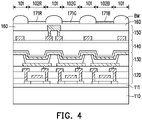
- FIG. 4 is a cross-sectional view showing a process of a method for manufacturing a display device according to another embodiment of the disclosure.
- FIG. 4 shows a step continuing FIG. 3D and replacing FIG. 3E to FIG. 3G .
- the same materials or methods may apply to the same or similar components in the embodiment of FIG. 4 and the embodiment of FIG. 3A to FIG. 3H , so the same and similar descriptions in the two embodiments will not be repeated herein, and the main difference between the two embodiments will be described.
- a black matrix layer BM is formed on the insulating layer 160.
- the black matrix layer BM may include a patterned black matrix layer and is disposed corresponding to the non-light-emitting region 101.
- the black matrix layer BM may expose the light-emitting region 102R, the light-emitting region 102G, and the light-emitting region 102B on the insulating layer 160.
- a red color filter layer 171R is formed on the insulating layer 160 and is disposed corresponding to the light-emitting region 102R
- a green color filter layer 171G is formed on the insulating layer 160 and is disposed corresponding to the light-emitting region 102G
- a blue color filter layer 171B is formed on the insulating layer 160 and is disposed corresponding to the light-emitting region 102B.
- the black matrix layer BM replaces the stack of three color filter layers located in the non-light-emitting region 101 in FIG. 3G and may have the effect of shielding light or as a blocking wall.
- the expression "corresponding to" described in the disclosure may mean, for example, that at least part of a component A and at least part of a component B overlap with each other in the normal direction of the substrate 110, or the component A and the component B completely overlap with each other.
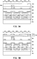
- FIG. 5A and FIG. 5B are cross-sectional views showing a process of a method for manufacturing a display device according to another embodiment of the disclosure.
- FIG. 5A and FIG. 5B show steps continuing FIG. 3D and replacing FIG. 3E to FIG. 3G .
- the same materials or methods may apply to the same or similar components in the embodiment of FIG. 5A to FIG. 5B and the embodiment of FIG. 3A to FIG. 3H , so the same and similar descriptions in the two embodiments will not be repeated herein, and the main difference between the two embodiments will be described.
- the anti-reflection layer 170a of this embodiment includes a yellow color filter layer 171Y and a blue color filter layer 171B.
- the yellow color filter layer 171Y is first formed on the insulating layer 160 and is disposed corresponding to the light-emitting region 102R, the light-emitting region 102G, and the non-light-emitting region 101, but is not disposed corresponding to the light-emitting region 102B.
- the blue color filter layer 171B is formed on the insulating layer 160 and the color filter layer 171Y by the above method and is disposed corresponding to the light-emitting region 102B and the non-light-emitting region 101, but is not disposed corresponding to the light-emitting region 102R and the light-emitting region 102G.
- the stack of two color filter layers i.e., the stack of the color filter layer 171Y and the color filter layer 171B) disposed on the non-light-emitting region 101 may have a light-shielding effect.
- FIG. 6A and FIG. 6B are respectively cross-sectional views showing a process of a method for manufacturing a display device according to some embodiments of the disclosure.
- FIG. 6A shows a step continuing FIG. 3D and replacing FIG. 3E to FIG. 3G .
- the same materials or methods may apply to the same or similar components in the embodiment of FIG. 6A (or the embodiment of FIG. 6B ) and the embodiment of FIG. 3A to FIG. 3H , so the same and similar descriptions in the two embodiments will not be repeated herein, and the main difference between the two embodiments will be described.
- step S260 and step S260b are performed to form an anti-reflection layer 170b on the insulating layer 160, and the anti-reflection layer 170b includes a polarizer 173.
- the anti-reflection layer 170b may have a multi-layer structure, a continuous structure, or a patterned structure, and the anti-reflection layer 170b further includes a first intermediate layer 172, a second intermediate layer 174, and a linear polarizer 175.
- the first intermediate layer 172 is disposed on the insulating layer 160
- the second intermediate layer 174 is disposed on the polarizer 173
- the linear polarizer 175 is disposed on the second intermediate layer 174.
- the first intermediate layer 172 and the second intermediate layer 174 are respectively disposed on two sides of the polarizer 173 to protect the polarizer 173 and increase attachment between the polarizer 173 and the insulating layer 160 (or the linear polarizer 175).
- the polarizer 173 in the anti-reflection layer 170b, may also be disposed directly on the insulating layer 160, and the linear polarizer 175 may be disposed directly on the polarizer 173 without the first intermediate layer 172 and the second intermediate layer 174 (not shown).
- the first intermediate layer 172, the polarizer 173, and the second intermediate layer 174 are sequentially formed directly on the insulating layer 160 by, for example, a coating process.
- the first intermediate layer 172, the polarizer 173, and the second intermediate layer 174 are all disposed corresponding to the light-emitting region 102R, the light-emitting region 102G, the light-emitting region 102B, and the non-light-emitting region 101.
- the materials of the first intermediate layer 172 and the second intermediate layer 174 may include an organic material.
- the first intermediate layer 172 and the second intermediate layer 174 may optionally not include an adhesive material, but the disclosure is not limited thereto.
- the material of the polarizer 173 includes, for example, a quarter wave plate (QWP).
- the wavelength of the polarizer 173 is, for example, the average value of the red wavelength, the green wavelength, and the blue wavelength, and is, for example, 550 nanometers (nm), but the disclosure is not limited thereto.
- a thickness T10 of the first intermediate layer 172 is, for example, 0.01 ⁇ m to 0.1 ⁇ m but is not limited thereto.
- a thickness T11 of the polarizer 173 is, for example, 1000 ⁇ m to 5000 ⁇ m but is not limited thereto.
- a thickness T12 of the second intermediate layer 174 is, for example, 0.05 ⁇ m to 1 ⁇ m but is not limited thereto.
- the linear polarizer 175 is formed directly on the second intermediate layer 174 by, for example, a coating process, and processes of aligning and baking (e.g., at 80°C to 100°C, but the disclosure is not limited thereto) the linear polarizer 175 are performed, but the disclosure is not limited thereto.
- the linear polarizer 175 may also be formed on the second intermediate layer 174 by, for example, a blade coating process, and the linear polarizer 175 may be aligned at the same time; then, the baking process of the linear polarizer 175 is performed.
- the alignment may include, for example, causing molecules in the linear polarizer 175 to be arranged in an orderly manner, so that the linear polarizer 175 can have a polarization function in a specific direction.
- an anti-reflection layer 170c of this embodiment is similar to the anti-reflection layer 170b of FIG. 6A , and the main difference between the two lies in that the anti-reflection layer 170c of this embodiment may include a polarizer 173a, a polarizer 173b, and a polarizer 173c designed for the light-emitting element 133 of different colors (the red light-emitting diode 133R, the green light-emitting diode 133G, and the blue light-emitting diode 133B).
- the polarizer 173a is disposed corresponding to at least the light-emitting region 102R but is not disposed corresponding to the light-emitting region 102G and the light-emitting region 102B
- the polarizer 173b is disposed corresponding to at least the light-emitting region 102G but is not disposed corresponding to the light-emitting region 102R and light-emitting region 102B
- the polarizer 173c is disposed corresponding to at least the light-emitting region 102B but is not disposed corresponding to the light-emitting region 102R and the light-emitting region 102G.
- the wavelength of the polarizer 173a is, for example, 1/4 of the red wavelength
- the wavelength of the polarizer 173b is, for example, 1/4 of the green wavelength
- the wavelength of the polarizer 173c is, for example, 1/4 of the blue wavelength, but the disclosure is not limited thereto.
- FIG. 7 is a cross-sectional view showing a process of a method for manufacturing a display device according to another embodiment of the disclosure.
- FIG. 7 shows a step continuing FIG. 3D and replacing FIG. 3E to FIG. 3G .
- the same materials or methods may apply to the same or similar components in the embodiment of FIG. 7 and the embodiment of FIG. 3A to FIG. 3H , so the same and similar descriptions in the two embodiments will not be repeated herein, and the main difference between the two embodiments will be described.
- step S260 and step S260c are performed to form an anti-reflection layer 170e on the insulating layer 160.
- the anti-reflection layer 170e includes a wire-grid polarizer (WGP) 176, and the wire-grid polarizer 176 may include a patterned wire-grid polarizer.
- WGP wire-grid polarizer
- the following two methods are adopted to form the wire-grid polarizer 176 directly on the insulating layer 160, but the disclosure is not limited thereto.
- the wire-grid polarizer 176 is deposited on the insulating layer 160 to directly cover the insulating layer 160; next, a plurality of openings 176a are formed by a photolithography process to expose the insulating layer 160; and then, a blackening treatment (e.g., oxidation) is performed to reduce reflection caused by the wire-grid polarizer 176.
- a blackening treatment e.g., oxidation
- the wire-grid polarizer 176 is formed directly on the insulating layer 160 by nanoimprint lithography, so that the wire-grid polarizer 176 directly covers the insulating layer 160 and has a plurality of openings 176a exposing the insulating layer 160; and then, a blackening treatment (e.g., oxidation) is performed to reduce reflection caused by the wire-grid polarizer 176.
- a blackening treatment e.g., oxidation
- an insulating layer 177 is formed on the wire-grid polarizer 176 and in the openings 176a of the wire-grid polarizer 176.
- the material of the wire-grid polarizer 176 may include aluminum, silver, platinum, gold, or a metal compound but is not limited thereto.
- FIG. 8A and FIG. 8B are schematic partial cross-sectional views of a display device according to some embodiments of the disclosure.
- a display device 100b (or a display device 100c) of this embodiment is substantially similar to the display device 100 of FIG. 1 , so the same and similar components in the two embodiments will not be repeatedly described herein.
- the main difference between the display device 100b (or the display device 100c) of this embodiment and the display device 100 lies in that the display device 100b (or the display device 100c) further includes an insulating layer 161 (or an insulating layer 162).
- the insulating layer 161 is disposed between the insulating layer 160 and the touch sensing unit 150.
- the insulating layer 161 has a plurality of recesses 161a, and the recesses 161a do not penetrate the insulating layer 161.
- the recess 161a may be disposed corresponding to the non-light-emitting region 101, but is not disposed corresponding to the light-emitting regions 102R, 102G, and 102B, so that the recess 161a can scatter external light to improve the anti-reflection effect.
- the insulating layer 162 of the display device 100c is disposed between the insulating layer 160 and the touch sensing unit 150 and has a plurality of rough surfaces 162a.
- the rough surface 162a may be disposed corresponding to the non-light-emitting region 101, but is not disposed corresponding to the light-emitting regions 102R, 102G, and 102B, so that the rough surface 162a can scatter external light to improve the anti-reflection effect.
- FIG. 9 is a schematic top view of a display device according to another embodiment of the disclosure.
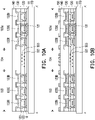
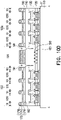
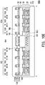
- FIG. 10A to FIG. 10E are cross-sectional views showing a process of a method for manufacturing the display device of FIG. 9 taken along section line A-A'.
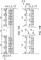
- FIG. 11A to FIG. 11C are cross-sectional views showing a process of a method for manufacturing the display device of FIG. 9 taken along section line B-B'.
- FIG. 9 omits several components in a display device 100d.
- the anti-reflection layer 170 and/or the cover layer 180 of island regions 103, 103a, and 103b in the display device 100d may be designed according to any of the above embodiments. The description below is based on a design similar to that shown in FIG. 3H , but the disclosure is not limited thereto.
- the display device 100d includes a plurality of island regions 103, 103a, and 103b, a plurality of bridge regions 104, and a plurality of opening regions 105.
- the island regions 103, 103a, and 103b are separate from each other and each includes a plurality of light-emitting units 130.
- the bridge regions 104 are respectively disposed between two adjacent island regions (e.g., between the island region 103 and the island region 103a, or between the island region 103a and the island region 103b), and are configured to connect two adjacent island regions (e.g., the island region 103 and the island region 103a, or the island region 103a and the island region 103b).
- the opening regions 105 have holes 190 which penetrate the display device 100d.
- the opening regions 105 are respectively disposed between two adjacent island regions (e.g., between the island region 103 and the island region 103b) to isolate two adjacent island regions (e.g., the island region 103 and the island region 103b) by the hole 190.
- the island regions 103, 103a, and 103b can be separate from each other, and the display device 100d of this embodiment can be stretchable.
- the stretchable display device 100d may be fit on an irregular surface (e.g., a spherical surface, a curved surface, an undulating surface, etc.) or may be stretched and enlarged for use.
- stretchable mentioned in this disclosure may mean, for example, that the size of the display device may be stretched from 5 inches to 6 inches, or the distance between the island region 103 and the island region 103a or between the island region 103a and the island region 103b of the display device may be changed by any operation, but the disclosure is not limited thereto.
- the same materials or methods may apply to the same or similar components and the same and similar descriptions in the two embodiments will not be repeated herein.
- the difference between the embodiment shown in FIG. 10A to FIG. 10E and the embodiment shown in FIG. 3A to FIG. 3H lies in that the method for manufacturing the display device 100d of this embodiment further includes forming the bridge region 104 between the island region 103 and the island region 103a adjacent to each other.
- a pixel circuit 120 is formed on the substrate 110, a light-emitting unit 130 is formed on the pixel circuit 120, an encapsulation layer 140 is formed on the light-emitting unit 130, and a touch sensing unit 150 is formed on the light-emitting unit 130.
- a transistor 121 in the pixel circuit 120 and the light-emitting unit 130 are both disposed in the island regions 103 and 103a, but are not disposed in the bridge region 104.
- a metal layer GE1 may be disposed on a gate insulating layer GI, and a metal layer SD3 may be disposed on an insulating layer 122.
- the light-emitting unit 130 includes a red light-emitting diode 133R, a green light-emitting diode 133G, and a blue light-emitting diode 133B.
- the touch sensing unit 150 is disposed on the encapsulation layer 140 in the island regions 103 and 103a and the bridge region 104, so that the touch sensing unit 150 in the island regions 103 and 103a and the touch sensing unit 150 in the bridge region 104 may be located on the same horizontal plane and may be easier to manufacture.
- an anti-reflection layer 170 is formed on the insulating layer 160, and the anti-reflection layer 170 includes a red color filter layer 171R, a green color filter layer 171G, and a blue color filter layer 171B.
- the red color filter layer 171R is disposed on the insulating layer 160 and is disposed corresponding to the light-emitting region 102R (i.e., the light-emitting region of the red light-emitting diode 133R) and the non-light-emitting region 101 in the island regions 103 and 103a and the bridge region 104.
- the green color filter layer 171G is disposed on the insulating layer 160 and the color filter layer 171R and is disposed corresponding to the light-emitting region 102G and the non-light-emitting region 101 in the island regions 103 and 103a and the bridge region 104.
- the blue color filter layer 171B is disposed on the insulating layer 160 and the color filter layer 171G and is disposed corresponding to the light-emitting region 102B and the non-light-emitting region 101 in the island regions 103 and 103a and the bridge region 104.
- a groove 191 is formed at the junction between the island regions 103 and 103a and the bridge region 104, and a cover layer 180 is formed on the anti-reflection layer 170 and in the groove 191.
- the groove 191 may be formed by, for example, etching, laser drilling, or a combination of the above but is not limited thereto.
- the groove 191 may expose part of the insulating layer 123 in the pixel circuit 120, and the groove 191 does not penetrate the substrate 110, so stress can be released accordingly.
- the cover layer 180 may cover the anti-reflection layer 170 and a sidewall 106 of the display device 100d. So far, the island regions 103 and 103a and the bridge region 104 in the display device 100d of this embodiment have been completed.
- FIG. 11A to FIG. 11C is similar to the embodiment shown in FIG. 3A to FIG. 3H , the same materials or methods may apply to the same or similar components and the same and similar descriptions in the two embodiments will not be repeated herein.
- the difference between the embodiment shown in FIG. 11A to FIG. 11C and the embodiment shown in FIG. 3A to FIG. 3H lies in that the method for manufacturing the display device 100d of this embodiment further includes forming an opening region 105 between the island region 103 and the island region 103b adjacent to each other.
- FIG. 11A to FIG. 11C may be regarded as steps continuing FIG. 10C and replacing FIG. 10D to FIG. 10E , and the manufacturing continues with the island region 103b and the opening region 105 in FIG. 11A to FIG. 11C respectively replacing the island region 103a and the bridge region 104 in FIG. 10A to FIG. 10C .
- the anti-reflection layer 170, the insulating layer 160, the touch sensing unit 150, the encapsulation layer 140, and the light-emitting unit 130 of the opening region 105 are etched and/or drilled to form a hole 192.
- the hole 192 may expose part of the insulating layer 123 in the pixel circuit 120.
- the pixel circuit 120 and the substrate 110 of the opening region 105 are etched and/or drilled to form a hole 193.
- the hole 192 is connected to the hole 193 to form a hole 190 penetrating the display device 100d.
- a sidewall 192a of the hole 192 and a sidewall 193a of the hole 193 may be rough surfaces. It is possible that the sidewall 192a of the hole 192 and the sidewall 193a of the hole 193 are not flush with each other.
- the hole 192 and the hole 193 in this embodiment are formed in two steps, in some embodiments, the hole 192 and the hole 193 may also be formed simultaneously in one step. In this embodiment, the hole 192 and the hole 193 may be formed by, for example, etching, laser drilling, or a combination of the above but are not limited thereto.
- a cover layer 180 is formed on the anti-reflection layer 170, in the hole 192, and in the hole 193.
- the cover layer 180 may cover the anti-reflection layer 170, the sidewall 106 of the display device 100d, the sidewall 192a of the hole 192, and the sidewall 193a of the hole 193. So far, the island regions 103 and 103b and the opening region 105 in the display device 100d of this embodiment have been completed.
- FIG. 12A to FIG. 12C are cross-sectional views showing a process of a method for manufacturing the display device of FIG. 9 taken along section line A-A' according to another embodiment. Since the embodiment shown in FIG. 12A to FIG. 12C is similar to the embodiment shown in FIG. 10A to FIG. 10E , the same materials or methods may apply to the same or similar components and the same and similar descriptions in the two embodiments will not be repeated herein. The difference between the embodiment shown in FIG. 12A to FIG. 12C and the embodiment shown in FIG. 10A to FIG.
- 10E lies in that, in the method for manufacturing the bridge region 104 of a display device 100e of this embodiment, first, a hole 191' is formed in the bridge region 104, and then a touch sensing unit 150' and an anti-reflection layer 170' are formed in the island regions 103 and 103a and the bridge region 104.
- the hole 191' is formed in the bridge region 104 so that the hole 191' can expose part of the insulating layer 123 in the pixel circuit 120.
- the touch sensing unit 150' is formed on the encapsulation layer 140 in the island regions 103 and 103a and in the hole 191' in the bridge region 104.
- the touch sensing unit 150' in the bridge region 104 is disposed on the insulating layer 123 in the hole 191', the touch sensing unit 150' in the bridge region 104 may be closer to the pixel circuit 120 and the light-emitting unit 130, so that the stress of the bridge region 104 can be more concentrated and easier to adjust or the bridge region 104 may have a better stretching effect .
- the anti-reflection layer 170' is formed on the insulating layer 160, and a cover layer 180' is formed on the anti-reflection layer 170'.
- the anti-reflection layer 170' may be disposed on the insulating layer 160 in the island regions 103 and 103a and on the insulating layer 160 in the hole 191' in the bridge region 104.
- the cover layer 180' may be disposed on the anti-reflection layer 170' in the island regions 103 and 103a and on the anti-reflection layer 170' in the hole 191' in the bridge region 104. So far, the island regions 103 and 103a and the bridge region 104 in the display device 100e of this embodiment have been completed.
- the opening region of the display device 100e in this embodiment may also be manufactured by a method different from that in FIG. 11A to FIG. 11C .
- the main difference between the method for manufacturing the opening region of this embodiment and the manufacturing method of FIG. 11A to FIG. 11C lies in that, in the method for manufacturing the opening region of the display device 100e of this embodiment, first, a hole which exposes part of the insulating layer 123 in the pixel circuit 120 is formed in the opening region, which is similar to the step shown in FIG. 12A (when the bridge region 104 in FIG. 12A is regarded as the opening region, and the island region 103a is regarded as the island region 103b).
- a touch sensing unit 150' and an anti-reflection layer 170' are formed in the island regions 103 and 103b, which similar to the step shown in FIG. 11A .
- a hole penetrating the display device 100e is formed in the opening region, which is similar to the step shown in FIG. 11B .
- a cover layer 180 is formed on the anti-reflection layer 170', which is similar to the step shown in FIG. 11C . So far, the island regions 103, 103b and the opening region in the display device 100e of this embodiment have been completed.
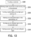
- FIG. 13 is a flowchart of a method for manufacturing a display device according to another embodiment of the disclosure.
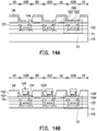
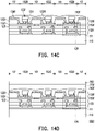
- FIG. 14A to FIG. 14D are cross-sectional views showing a process of a method for manufacturing a display device according to another embodiment of the disclosure. Since the embodiment shown in FIG. 2 (or FIG. 3A to FIG. 3H ) is similar to the embodiment shown in FIG. 13 (or FIG. 14A to FIG. 14D ), the same materials or methods may apply to the same or similar components and the same and similar descriptions in the two embodiments will not be repeated herein. The difference between the embodiment shown in FIG. 2 (or FIG. 3A to FIG. 3H ) and the embodiment shown in FIG. 13 (or FIG. 14A to FIG. 14D ) lies in that, in the method for manufacturing a display device 100f of this embodiment, a light-emitting element 133f is formed on the pixel circuit 120 by transfer and bonding.
- step S300 and step S310 are performed to provide a substrate 110 and form a pixel circuit 120 and a touch sensing unit 150f on the substrate 110.
- a buffer layer 111 is further included between the pixel circuit 120 and the substrate 110.
- the touch sensing unit 150f may include a first metal layer 151f and an insulating layer 152f.
- the first metal layer 151f and the insulating layer 152f are adjacently disposed on the insulating layer 123 of the pixel circuit 120.
- the first metal layer 151f is disposed corresponding to the non-light-emitting region 101, but is not disposed corresponding to the light-emitting regions 102R, 102G, and 102B.
- step S320 is performed to form a light-emitting unit 130f on the touch sensing unit 150f.
- the light-emitting unit 130f includes a first electrode 131f, an insulating layer 132f, a light-emitting element 133f, and a second electrode 134f.
- the first electrode 131f and the second electrode 134f are adjacently disposed on the insulating layer 152f.
- the insulating layer 132f is disposed on the first electrode 131f and the second electrode 134f.
- the insulating layer 132f has an opening 132f1 to expose part of the first electrode 131f and part of the second electrode 134f.
- the light-emitting element 133f which has been completed is transferred into the opening 132f1 to bond to the first electrode 131f and the second electrode 134f in the opening 132f1 and electrically connect to the transistor 121 via the first electrode 131f.
- the light-emitting element 133f may be, for example, a flip-chip micro light-emitting diode but is not limited thereto.
- the light-emitting element 133f may include a red light-emitting diode, a green light-emitting diode, and a blue light-emitting diode but is not limited thereto. In some embodiments, the light-emitting element 133f may also be a blue light-emitting diode.
- step S330, step S340, and step S350 are performed to form an encapsulation layer 140f on the light-emitting unit 130f, form an anti-reflection layer 170f on the encapsulation layer 140f, and form a cover layer 180 on the anti-reflection layer 170f.
- the encapsulation layer 140f may be disposed in the opening 132f1 and may cover the light-emitting element 133f and the second electrode 134f.
- the anti-reflection layer 170f may include a color filter layer, a polarizer, or a wire-grid polarizer. So far, the display device 100f of this embodiment has been completed.
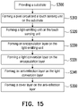
- FIG. 15 is a flowchart of a method for manufacturing a display device according to another embodiment of the disclosure.
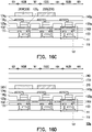
- FIG. 16A to FIG. 16D are cross-sectional views showing a process of a method for manufacturing a display device according to another embodiment of the disclosure. Since the embodiment shown in FIG. 13 (or FIG. 14A to FIG. 14D ) is similar to the embodiment shown in FIG. 15 (or FIG. 16A to FIG. 16D ), the same materials or methods may apply to the same or similar components and the same and similar descriptions in the two embodiments will not be repeated herein. The difference between the embodiment shown in FIG. 13 (or FIG. 14A to FIG. 14D ) and the embodiment shown in FIG. 15 (or FIG. 16A to FIG. 16D ) lies in that, the method for manufacturing a display device 100g of this embodiment further includes forming a light conversion layer 200 on an encapsulation layer 140g.
- steps S300 and S310 are performed to provide a substrate 110 and form a pixel circuit 120 and a touch sensing unit 150f on the substrate 110.
- a buffer layer 111 is further included between the pixel circuit 120 and the substrate 110.
- the touch sensing unit 150f may include a first metal layer 151f and an insulating layer 152f.
- the first metal layer 151f and the insulating layer 152f are adjacently disposed on an insulating layer 123 of the pixel circuit 120.
- the first metal layer 151f is disposed corresponding to the non-light-emitting region 101 but is not disposed corresponding to the light-emitting regions 102R, 102G, and 102B.
- step S320 is performed to form a light-emitting unit 130g on the touch sensing unit 150f.
- the light-emitting unit 130g includes a first electrode 131g, an insulating layer 132g, a light-emitting element 133g, a second electrode 134g, and an insulating layer 135g.
- the first electrode 131g is disposed on the insulating layer 152f.
- the insulating layer 132g is disposed on the first electrode 131g.
- the insulating layer 132g has an opening 132g1 to expose part of the first electrode 131g.
- the light-emitting element 133g which has been completed is transferred into the opening 132g1 to bond to the first electrode 131g in the opening 132g1 and electrically connect to the transistor 121 via the first electrode 131g.
- the insulating layer 135g is disposed on the insulating layer 132g and in the opening 132g1 to cover the light-emitting element 133g.
- the second electrode 134g is disposed on the insulating layer 135g and is electrically connected to the light-emitting element 133g.
- the light-emitting element 133g may be, for example, a vertical micro light-emitting diode or a vertical nano light-emitting diode (nano-LED) but is not limited thereto.
- the light-emitting element 133g may include a blue light-emitting diode but is not limited thereto.
- step S330 and step S331 are performed to form an encapsulation layer 140g on the light-emitting unit 130g and form a light conversion layer 200 on the encapsulation layer 140g.
- the encapsulation layer 140g may cover the insulating layer 135g and the second electrode 134g.
- the light conversion layer 200 may include a red light conversion layer 200R and a green light conversion layer 200G respectively disposed corresponding to one of the light-emitting elements 133g.
- the light conversion layer 200 may include, for example, quantum dots but is not limited thereto.
- step S341 and step S350 are performed to form an anti-reflection layer 170f on the light conversion layer 200 and form a cover layer 180 on the anti-reflection layer 170f.
- an insulating layer 210 may be further formed on the light conversion layer 200, so that the insulating layer 210 can cover the light conversion layer 200 and the insulating layer 135g.
- the anti-reflection layer 170f may include a color filter layer, a polarizer, or a wire-grid polarizer. So far, the display device 100g of this embodiment has been completed.
- the method of forming the anti-reflection layer on the insulating layer in the embodiments of the disclosure can reduce the overall thickness, reduce the bending stress, improve the reliability, or increase the service life.
- the display device is a foldable display device or a stretchable display device
- the display device when the display device is to be bent, rolled, or stretched, compared to the method of attaching an anti-reflection layer externally onto the insulating layer
- the method of forming the anti-reflection layer on the insulating layer in the embodiments of the disclosure can reduce the bending stress to suppress separation of the anti-reflection layer, which thereby improves the reliability of the display device or increases the service life of the display device.
Landscapes
- Engineering & Computer Science (AREA)
- General Engineering & Computer Science (AREA)
- Theoretical Computer Science (AREA)
- Physics & Mathematics (AREA)
- Human Computer Interaction (AREA)
- General Physics & Mathematics (AREA)
- Microelectronics & Electronic Packaging (AREA)
- Manufacturing & Machinery (AREA)
- Optics & Photonics (AREA)
- Electroluminescent Light Sources (AREA)
- Devices For Indicating Variable Information By Combining Individual Elements (AREA)
Abstract
Description
- The disclosure relates to a method for manufacturing a display device, and more particularly, to a method for manufacturing a display device which can improve reliability.
- Display devices have been widely applied to electronic devices such as mobile phones, televisions, monitors, tablet computers, car displays, wearable devices, and desktop computers. With the vigorous development of electronic products, the requirements for the display quality of the display devices also increase, such that the display devices are constantly improving towards display effects of high brightness, low energy consumption, high resolution, or high saturation. Meanwhile, the method for manufacturing the display device is constantly improving towards reduced process time, reduced process steps, or an improved process sequence.
- The disclosure provides a method for manufacturing a display device which can improve the reliability of a display device such as improving the bending endurance of the display device, improving the service life of the display device, or improving both of the above, but the disclosure is not limited thereto.
- The disclosure provides a method for manufacturing a display device, including the following steps. A substrate is provided. A pixel circuit is formed on the substrate. A light-emitting unit is formed on the pixel circuit. A touch sensing unit is formed on the light-emitting unit. An insulating layer is formed on the touch sensing unit. An anti-reflection layer is formed on the insulating layer.
- The accompanying drawings are included to provide a further understanding of the disclosure, and are incorporated in and constitute a part of this specification. The drawings illustrate embodiments of the disclosure and, together with the description, serve to explain the principles of the disclosure.
-
FIG. 1 is a schematic partial cross-sectional view of a display device according to some embodiments of the disclosure. -
FIG. 2 is a flowchart of a method for manufacturing a display device according to an embodiment of the disclosure. -
FIG. 3A to FIG. 3H are cross-sectional views showing a process of a method for manufacturing a display device according to some embodiments of the disclosure. -
FIG. 3H' andFIG. 3H " are partial cross-sectional views of a display device according to some embodiments of the disclosure. -
FIG. 4 is a cross-sectional view showing a process of a method for manufacturing a display device according to another embodiment of the disclosure. -
FIG. 5A and FIG. 5B are cross-sectional views showing a process of a method for manufacturing a display device according to another embodiment of the disclosure. -
FIG. 6A and FIG. 6B are respectively cross-sectional views showing a process of a method for manufacturing a display device according to some embodiments of the disclosure. -
FIG. 7 is a cross-sectional view showing a process of a method for manufacturing a display device according to another embodiment of the disclosure. -
FIG. 8A and FIG. 8B are schematic partial cross-sectional views of a display device according to some embodiments of the disclosure. -
FIG. 9 is a schematic top view of a display device according to another embodiment of the disclosure. -
FIG. 10A to FIG. 10E are cross-sectional views showing a process of a method for manufacturing the display device ofFIG. 9 taken along section line A-A'. -
FIG. 11A to FIG. 11C are cross-sectional views showing a process of a method for manufacturing the display device ofFIG. 9 taken along section line B-B'. -
FIG. 12A to FIG. 12C are cross-sectional views showing a process of a method for manufacturing the display device ofFIG. 9 taken along section line A-A' according to another embodiment. -
FIG. 13 is a flowchart of a method for manufacturing a display device according to another embodiment of the disclosure. -
FIG. 14A to FIG. 14D are cross-sectional views showing a process of a method for manufacturing a display device according to another embodiment of the disclosure. -
FIG. 15 is a flowchart of a method for manufacturing a display device according to another embodiment of the disclosure. -
FIG. 16A to FIG. 16D are cross-sectional views showing a process of a method for manufacturing a display device according to another embodiment of the disclosure. - The disclosure may be understood by referring to the following detailed description with reference to the accompanying drawings. It is noted that for comprehension of the reader and simplicity of the drawings, in the drawings of the disclosure, only a part of the electronic device is shown, and specific components in the drawings are not necessarily drawn to scale. Moreover, the quantity and the size of each component in the drawings are only schematic and are not intended to limit the scope of the disclosure.
- In the following specification and claims, the terms "having", "including", "comprising" etc. are open-ended terms, so they should be interpreted to mean "including but not limited to ...".
- It should be understood that when a component or a film layer is described as being "on" or "connected to" another component or film layer, it may be directly on or connected to the another component or film layer, or there is an intervening component or film layer therebetween (i.e., being indirectly on or indirectly connected). Conversely, when a component or film layer is described as being "directly on" or "directly connected to" another component or film layer, there is no intervening component or film layer therebetween.
- The terms such as "first", "second", "third", etc. may be used to describe components, but the components should not be limited by these terms. The terms are only intended to distinguish a component from another component in the specification. It is possible that the claims do not use the same terms and replace the terms with "first", "second", "third" etc. according to the sequence declared in the claims. Accordingly, in the specification, a first component may be described as a second component in the claims.
- In some embodiments of the disclosure, unless specifically defined, terms related to bonding and connection such as "connect", "interconnect", etc. may mean that two structures are in direct contact, or that two structures are not in direct contact and another structure is provided therebetween. The terms related to bonding and connection may also cover cases where two structures are both movable or two structures are both fixed. In addition, the term "couple" includes any direct and indirect electrical connection means.
- In the disclosure, a length, width, thickness, height, or area, or a distance or spacing between components may be measured by optical microscopy (OM), a scanning electron microscope (SEM), a film thickness profile measuring instrument (a-step), an ellipsometer, or other suitable methods. Specifically, according to some embodiments, a cross-sectional structure image containing components to be measured may be obtained by a scanning electron microscope to measure the width, thickness, height, or area of each component, or the distance or spacing between the components, but the disclosure is not limited thereto. In addition, there may be a certain error between any two values or directions used for comparison.
- In the disclosure, the terms such as "approximately", "about", or "substantially" are generally interpreted as one value being within a range of plus or minus 10%, plus or minus 5%, plus or minus 3%, plus or minus 2%, plus or minus 1%, or plus or minus 0.5% of a given value. Herein, a given value refers to an approximate value, i.e., in the absence of a specific expression of "approximately", "about", or "substantially", the meaning of "approximately", "about", or "substantially" may still be implied. In addition, the expression "a given range is between a first numerical value and a second numerical value" means that the given range includes the first numerical value, the second numerical value, and other values therebetween.
- The electronic device of the disclosure may include a display device, an antenna device (e.g., a liquid crystal antenna), a sensing device, a light-emitting device, a touch device, or a splicing device, but is not limited thereto. The electronic device may include a bendable or flexible electronic device. The shape of the electronic device may be rectangular, circular, polygonal, a shape with curved edges, or other suitable shapes. The display device may include, for example, a light-emitting diode (LED), a liquid crystal, a fluorescence, a phosphor, a quantum dot (QD), other suitable materials, or a combination of the above, but is not limited thereto. The light-emitting diode may include, for example, an organic light-emitting diode (OLED), an inorganic light-emitting diode, a mini LED, a micro LED, a quantum dot LED (QLED or QDLED), other suitable materials, or any combination of the above, but is not limited thereto. The display device may include, for example, a splicing display device but is not limited thereto. The antenna device may include, for example, a liquid crystal antenna but is not limited thereto. The antenna device may include, for example, an antenna splicing device but is not limited thereto. It is noted that the electronic device may be any combination of the above but is not limited thereto. The electronic device may have peripheral systems such as a driving system, a control system, a light source system, a rack system, etc. to support a display device, an antenna device, or a splicing device. Hereinafter, a display device will be described to illustrate the content of the disclosure, but the disclosure is not limited thereto.
- In the disclosure, the features in multiple different embodiments descried below may be replaced, combined, and/or mixed to form other embodiments without departing from the spirit of the disclosure. The features of the embodiments may be arbitrarily mixed and combined as long as they do not depart from or conflict with the spirit of the disclosure.
-
FIG. 1 is a schematic partial cross-sectional view of a display device according to some embodiments of the disclosure. Referring toFIG. 1 , adisplay device 100 of this embodiment includes the following components sequentially from bottom to top: asubstrate 110, apixel circuit 120, a light-emittingunit 130, anencapsulation layer 140, atouch sensing unit 150, an insulatinglayer 160, ananti-reflection layer 170, and acover layer 180. In this embodiment, thesubstrate 110 has a thickness T1. The thickness T1 is, for example, the maximum thickness of thesubstrate 110 measured along the normal direction of thesubstrate 110. Thesubstrate 110 may include a rigid substrate, a flexible substrate, or a combination of the above. For example, the material of thesubstrate 110 may include glass, quartz, sapphire, ceramic, polycarbonate (PC), polyimide (PI), polyethylene terephthalate (PET), other suitable substrate materials, or combinations of the above, but is not limited thereto. - The
pixel circuit 120 is disposed on thesubstrate 110 and includes atransistor 121. The light-emittingunit 130 is disposed on thepixel circuit 120 and is electrically connected to thetransistor 121 in thepixel circuit 120. - The
encapsulation layer 140 is disposed on the light-emittingunit 130. Theencapsulation layer 140 includes a first insulatinglayer 141, aplanarizing layer 142, and a second insulatinglayer 143. The first insulatinglayer 141 is disposed on the light-emittingunit 130 and has a thickness T2. Theplanarizing layer 142 is disposed on the first insulatinglayer 141 and has a thickness T3. The secondinsulating layer 143 is disposed on theplanarizing layer 142 and has a thickness T4. The thickness T2 is, for example, the maximum thickness of the first insulatinglayer 141 measured along the normal direction of thesubstrate 110. The thickness T3 is, for example, the maximum thickness of theplanarizing layer 142 measured along the normal direction of thesubstrate 110. The thickness T4 is, for example, the maximum thickness of the second insulatinglayer 143 measured along the normal direction of thesubstrate 110. In this embodiment, the first insulatinglayer 141, theplanarizing layer 142, and the second insulatinglayer 143 may respectively have a single-layer structure or a multi-layer structure. The materials of the first insulatinglayer 141 and the second insulatinglayer 143 may include, for example, an inorganic material (e.g., silicon nitride or other suitable inorganic materials) but are not limited thereto. The material of theplanarizing layer 142 may include, for example, an organic material but is not limited thereto. - In this embodiment, the thickness T4 of the second insulating
layer 143 is, for example, greater than the thickness T2 of the first insulating layer 141 (i.e., T4>T2), but the disclosure is not limited thereto. The ratio of the thickness T4 of the second insulatinglayer 143 to the thickness T2 of the first insulatinglayer 141 is, for example, greater than 1 and less than or equal to 3 (i.e., 1<T4/T2≤3), but the disclosure is not limited thereto. The thickness T3 of theplanarizing layer 142 is, for example, greater than the sum of the thickness T2 of the first insulatinglayer 141 and the thickness T4 of the second insulating layer 143 (i.e., T3>T2+T4), but the disclosure is not limited thereto. The ratio of the thickness T3 of theplanarizing layer 142 to the sum (i.e., the sum of the thickness T2 of the first insulatinglayer 141 and the thickness T4 of the second insulating layer 143) is, for example, greater than or equal to 3 and less than or equal to 6 (i.e., 3≤T3/(T2+T4) ≤6), but the disclosure is not limited thereto. In addition, in this embodiment, the thickness T2 of the first insulatinglayer 141 is, for example, greater than or equal to 0.5 µm and less than or equal to 1 µm (i.e., 0.5 µm≤T2≤1 µm) but is not limited thereto. The thickness T3 of theplanarizing layer 142 is, for example, greater than or equal to 5 µm and less than or equal to 10 µm (i.e., 5 µm≤T3≤10 µm) but is not limited thereto. The thickness T4 of the second insulatinglayer 143 is, for example, greater than or equal to 0.8 µm and less than or equal to 1.5 µm (i.e., 0.8 µm≤T4≤1.5 µm) but is not limited thereto. - The
touch sensing unit 150 is disposed on theencapsulation layer 140. The insulatinglayer 160 is disposed on thetouch sensing unit 150. Theanti-reflection layer 170 is disposed on the insulatinglayer 160 and has a thickness T5. The thickness T5 is, for example, the maximum thickness of theanti-reflection layer 170 measured along the normal direction of thesubstrate 110. Thecover layer 180 is disposed on theanti-reflection layer 170 and has a thickness T6. The thickness T6 is, for example, the maximum thickness of thecover layer 180 measured along the normal direction of thesubstrate 110. In addition, in this embodiment, the thickness T1 of thesubstrate 110 is, for example, greater than the thickness T5 of theanti-reflection layer 170 but is not limited thereto. The thickness T6 of thecover layer 180 is, for example, greater than the thickness T5 of theanti-reflection layer 170 but is not limited thereto. - Furthermore, the
display device 100 of this embodiment further includes abuffer layer 111. Thebuffer layer 111 is disposed between thepixel circuit 120 and thesubstrate 110. Thebuffer layer 111 may have a single-layer structure or a multi-layer structure, and thebuffer layer 111 may include an organic material, an inorganic material, or a combination of the above but is not limited thereto. - Other embodiments will be provided and described below. It is noted herein that the reference numerals and part of the descriptions of the above embodiment apply to the following embodiments, where the same numerals are used to represent the same or similar components, and descriptions of the same technical contents are omitted. Reference may be made to the above embodiment for the descriptions of the omitted contents, which will not be repeated in the following embodiments.
-
FIG. 2 is a flowchart of a method for manufacturing a display device according to an embodiment of the disclosure.FIG. 3A to FIG. 3H are cross-sectional views showing a process of a method for manufacturing a display device according to some embodiments of the disclosure.FIG. 3H' andFIG. 3H " are partial cross-sectional views of a display device according to some embodiments of the disclosure. - First, referring to
FIG. 2 andFIG. 3A at the same time, in a method for manufacturing adisplay device 100a of this embodiment, first, step S200 and step S210 are performed to provide asubstrate 110 and form apixel circuit 120 on thesubstrate 110. Specifically, thepixel circuit 120 may include atransistor 121, a gate insulating layer GI, an insulatinglayer 122, and an insulatinglayer 123. Thetransistor 121 may include a gate electrode GE, a portion of the gate insulating layer GI, a source electrode SD1, a drain electrode SD2, and a semiconductor SE. The semiconductor SE is disposed on thesubstrate 110, the gate insulating layer GI is disposed on the semiconductor SE, the gate electrode GE is disposed on the gate insulating layer GI, the insulatinglayer 122 is disposed on the gate electrode GE, the source electrode SD1 and the drain electrode SD2 are disposed on the insulatinglayer 122, and the insulatinglayer 123 is disposed on the source electrode SD1 and the drain electrode SD2. In this embodiment, the material of the semiconductor SE may include an amorphous silicon, a low temperature polysilicon (LTPS), a metal oxide (e.g., indium gallium zinc oxide (IGZO)), other suitable materials, or a combination of the above but is not limited thereto. In other embodiments, different transistors may include different semiconductor layer materials, but the disclosure is not limited thereto. Moreover, although thetransistor 121 of this embodiment is a top-gate transistor, the disclosure is not limited thereto. In other embodiments, the transistor may also include a bottom-gate transistor, a top-gate transistor, and/or a double-gate transistor, but the disclosure is not limited thereto. In addition, thedisplay device 100a of this embodiment further includes abuffer layer 111, and thebuffer layer 111 is disposed between the gate insulating layer GI of thepixel circuit 120 and thesubstrate 110. - Then, referring to
FIG. 2 andFIG. 3B at the same time, step S220 is performed to form a light-emittingunit 130 on thepixel circuit 120. Specifically, the light-emittingunit 130 includes afirst electrode 131, an insulatinglayer 132, a light-emittingelement 133, and asecond electrode 134. Thefirst electrode 131 is disposed on the insulatinglayer 123. The insulatinglayer 132 is disposed on thefirst electrode 131. The insulatinglayer 132 has anopening 132a to expose part of thefirst electrode 131. The light-emittingelement 133 is disposed in theopening 132a and on thefirst electrode 131 to electrically connect to the drain electrode SD2 of thetransistor 121 via thefirst electrode 131. Thesecond electrode 134 is disposed on the insulatinglayer 132 and in theopening 132a and is electrically connected to the light-emittingelement 133. In this embodiment, a light-emitting element 133 (e.g., an organic light-emitting diode) may be formed (e.g., by deposition, but the disclosure is not limited thereto) directly on thefirst electrode 131, or a light-emitting element 133 (e.g., a micro light-emitting diode) which has been completed may be placed on thefirst electrode 131 by indirect transfer. The light-emittingelement 133 may include light-emitting diodes (LED) of different colors, e.g., a red light-emittingdiode 133R, a green light-emittingdiode 133G, and a blue light-emittingdiode 133B, but is not limited thereto. - Next, referring to
FIG. 2 andFIG. 3C at the same time, step S230 is performed to form anencapsulation layer 140 on the light-emittingunit 130. Specifically, theencapsulation layer 140 has a multi-layer structure, including a first insulatinglayer 141, aplanarizing layer 142, and a second insulatinglayer 143. The first insulatinglayer 141 is disposed on thesecond electrode 134 of the light-emittingunit 130. Theplanarizing layer 142 is disposed on the first insulatinglayer 141. The secondinsulating layer 143 is disposed on theplanarizing layer 142. The first insulatinglayer 141 and the second insulatinglayer 143 are respectively located on two opposite sides of theplanarizing layer 142. In addition, the arrangement of theplanarizing layer 142 may provide a substantially flat surface. Specifically, for example, thicknesses may be measured along the normal direction of thesubstrate 110 from the surface of theplanarizing layer 142 to the surface of thesubstrate 110, and when the difference between any two thicknesses is less than or equal to 1 µm, theplanarizing layer 142 may be regarded as flat, so that the subsequently manufactured layer (e.g., an anti-reflection layer 170) may have a better effect. - Then, referring to
FIG. 2 andFIG. 3D at the same time, step S240 and step S250 are performed to form atouch sensing unit 150 on the light-emittingunit 130 and form an insulatinglayer 160 on thetouch sensing unit 150. Specifically, thetouch sensing unit 150 may include afirst metal layer 151, an insulatinglayer 152, a conductive via 153, and asecond metal layer 154, and thefirst metal layer 151 and thesecond metal layer 154 may include a patterned conductive layer, but the disclosure is not limited thereto. Thefirst metal layer 151 is disposed on the second insulatinglayer 143 of theencapsulation layer 140. Thefirst metal layer 151 is disposed corresponding to a non-light-emittingregion 101 and is not disposed corresponding to light-emittingregions element 133 of this embodiment emits light in a direction away from thesubstrate 110, the light-emittingregions element 133. In other words, the light-emittingregions diode 133R, the green light-emittingdiode 133G, and the blue light-emittingdiode 133B) in the light-emitting direction of the light-emitting element 133 (the red light-emittingdiode 133R, the green light-emittingdiode 133G, and the blue light-emittingdiode 133B), and the non-light-emittingregion 101 may be defined as a region that does not overlap with the light-emitting element 133 (the red light-emittingdiode 133R, the green light-emittingdiode 133G, and the blue light-emittingdiode 133B) in the light-emitting direction of the light-emitting element 133 (the red light-emittingdiode 133R, the green light-emittingdiode 133G, and the blue light-emittingdiode 133B). The insulatinglayer 152 is disposed on thefirst metal layer 151. Thesecond metal layer 154 is disposed on the insulatinglayer 152 and is electrically connected to thefirst metal layer 151 via the conductive via 153 penetrating the insulatinglayer 152. In this embodiment, the materials of thefirst metal layer 151 and thesecond metal layer 154 may include, for example, a stack of three metal layers, in which the first layer and the third layer are titanium, and the second layer located between the first layer and the third layer is aluminum, but the disclosure is not limited thereto. The insulatinglayer 152 may have a single-layer structure or a multi-layer structure, and the insulatinglayer 152 may include an inorganic material (e.g., silicon nitride or other suitable inorganic materials) but is not limited thereto. - In this embodiment, a thickness T7 of the
first metal layer 151 is, for example, greater than or equal to 0.1 µm and less than or equal to 0.4 µm (i.e., 0.1 µm≤T7≤0.4 µm) but is not limited thereto. A thickness T8 of the insulatinglayer 152 is, for example, greater than or equal to 0.1 µm and less than or equal to 0.4 µm (i.e., 0.1 µm≤T8≤0.4 µm) but is not limited thereto. A thickness T9 of thesecond metal layer 154 is, for example, greater than or equal to 0.2 µm and less than or equal to 0.5 µm (i.e., 0.2 µm≤T9≤0.5 µm) but is not limited thereto. If the thickness T7 of thefirst metal layer 151 is less than 0.1 µm or the thickness T9 of thesecond metal layer 154 is less than 0.2 µm, the impedance will increase and signal transmission will be affected. If the thickness T7 of thefirst metal layer 151 is greater than 0.4 µm or the thickness T9 of thesecond metal layer 154 is greater than 0.5 µm, the topography will be uneven, which will affect the polarization effect of a subsequently manufacturedanti-reflection layer 170. In addition, in this embodiment, the thickness T9 of thesecond metal layer 154 is, for example, greater than the thickness T7 of the first metal layer 151 (i.e., T9>T7) but is not limited thereto. The thickness T9 of thesecond metal layer 154 is, for example, greater than the thickness T8 of the insulatinglayer 152, and the thickness T8 of the insulatinglayer 152 is, for example, greater than the thickness T7 of the first metal layer 151 (i.e., T9>T8>T7), but the disclosure is not limited thereto. The ratio of the thickness T9 of thesecond metal layer 154 to the thickness T7 of thefirst metal layer 151 is, for example, greater than or equal to 1 and less than or equal to 1.5 (i.e., 1≤T9/T7≤1.5), but the disclosure is not limited thereto. - In this embodiment, the insulating
layer 160 is disposed on the insulatinglayer 152 and thesecond metal layer 154 of thetouch sensing unit 150. The insulatinglayer 160 may have a single-layer structure or a multi-layer structure, and the insulatinglayer 160 may include an organic material, an inorganic material, or a combination of the above but is not limited thereto. - Then, referring to
FIG. 2 ,FIG. 3E ,FIG. 3F , andFIG. 3G at the same time, step S260 and step S260a are performed to form ananti-reflection layer 170 on the insulatinglayer 160. Theanti-reflection layer 170 may include, for example, a patterned anti-reflection layer but is not limited thereto, and theanti-reflection layer 170 may include acolor filter layer 171R, acolor filter layer 171G, and acolor filter layer 171B. In this embodiment, theanti-reflection layer 170 is formed on the insulatinglayer 160 by, for example, a semiconductor manufacturing process, and is not provided by adhering an anti-reflection layer which has been completed onto the insulatinglayer 160 through an adhesive layer. In this embodiment, theanti-reflection layer 170 may be formed directly on the insulatinglayer 160, so that there is no other layer between theanti-reflection layer 170 and the insulatinglayer 160. In this embodiment, theanti-reflection layer 170 may be formed on the insulatinglayer 160 by, for example, an ink-jet printing process, but disclosure does not specifically limit the formation method of theanti-reflection layer 170. Specifically, referring toFIG. 3E , by an ink-jet printing process, the redcolor filter layer 171R is formed on the insulatinglayer 160 and is disposed corresponding to the light-emittingregion 102R (i.e., the light-emitting region of the red light-emittingdiode 133R) and the non-light-emittingregion 101, but is not disposed corresponding to the light-emittingregion 102G (i.e., the light-emitting region of the green light-emittingdiode 133G) and the light-emittingregion 102B (i.e., the light-emitting region of the blue light-emittingdiode 133B). Next, referring toFIG. 3F , the greencolor filter layer 171G is formed on the insulatinglayer 160 and thecolor filter layer 171R and is disposed corresponding to the light-emittingregion 102G and the non-light-emittingregion 101, but is not disposed corresponding to the light-emittingregion 102R and the light-emittingregion 102B. Next, referring toFIG. 3G , the bluecolor filter layer 171B is formed on the insulatinglayer 160 and thecolor filter layer 171G and is disposed corresponding to the light-emittingregion 102B and the non-light-emittingregion 101, but is not disposed corresponding to the light-emittingregion 102R and the light-emittingregion 102G. The stack of three color filter layers (i.e., the stack of thecolor filter layer 171R, thecolor filter layer 171G, and thecolor filter layer 171B) disposed on the non-light-emittingregion 101 may have a light-shielding effect. So far, theanti-reflection layer 170 of this embodiment has been completed. - In some embodiments, the
anti-reflection layer 170 may also be formed on the insulatinglayer 160 by, for example, a coating process, and theanti-reflection layer 170 may also be formed on the insulatinglayer 160 by, for example, a photolithography process. Specifically, one layer of redcolor filter layer 171R is formed on the insulatinglayer 160 by a coating process, so that the redcolor filter layer 171R covers the light-emittingregion 102R, the light-emittingregion 102G, the light-emittingregion 102B, and the non-light-emitting region 101 (not shown). Next, the redcolor filter layer 171R is etched by a photolithography process to etch thecolor filter layer 171R on the light-emittingregion 102G and the light-emittingregion 102B and expose the insulatinglayer 160, as shown inFIG. 3E . Then, according to steps similar to those described above, the greencolor filter layer 171G is formed by a coating process and a photolithography process, so that the greencolor filter layer 171G is disposed in the light-emittingregion 102G and the non-light-emittingregion 101, and thecolor filter layer 171R of the light-emittingregion 102R and the insulatinglayer 160 of the light-emittingregion 102B are exposed, as shown inFIG. 3F . Then, according to steps similar to those described above, the bluecolor filter layer 171B is formed by a coating process and a photolithography process, so that the bluecolor filter layer 171B is disposed in the light-emittingregion 102B and the non-light-emittingregion 101, and thecolor filter layer 171R of the light-emittingregion 102R and thecolor filter layer 171G of the light-emittingregion 102G are exposed, as shown inFIG. 3G . - Although in the method for manufacturing the
display device 100a of this embodiment, the redcolor filter layer 171R is formed first, and then the greencolor filter layer 171G and the bluecolor filter layer 171B are formed, the disclosure does not specifically limit the sequence of forming the color filter layer. In some embodiments, the greencolor filter layer 171G or the bluecolor filter layer 171B may also be formed first. - Then, referring to
FIG. 2 andFIG. 3H at the same time, step S270 is performed to form acover layer 180 on theanti-reflection layer 170. In this embodiment, thecover layer 180 may be formed on theanti-reflection layer 170 by a coating process, but the disclosure does not specifically limit the formation method of thecover layer 180. Specifically, thecover layer 180 includes aplanarizing layer 181 and aplanarizing layer 182. In this embodiment, by a coating process, theplanarizing layer 181 is first formed on thecolor filter layer 171R of the light-emittingregion 102R, on thecolor filter layer 171G of the light-emittingregion 102G, on thecolor filter layer 171B of the light-emittingregion 102B, and on thecolor filter layer 171B of the non-light-emittingregion 101 to perform planarization. Then, theplanarizing layer 182 is formed on theplanarizing layer 181 by a coating process. Theplanarizing layer 181 and theplanarizing layer 182 may have a single-layer structure or a multi-layer structure, and theplanarizing layer 181 and theplanarizing layer 182 may include an organic material but are not limited thereto. For example, theplanarizing layer 181 and theplanarizing layer 182 may include polyethylene terephthalate, polyimide, or a combination of the above but are not limited thereto. So far, thedisplay device 100a of this embodiment has been completed. - In some embodiments, the
cover layer 180 may also be formed on theanti-reflection layer 170 by, for example, a coating process and an adhesion process. Referring toFIG. 3H' , thecover layer 180 includes aplanarizing layer 181, anadhesive layer 183, and asubstrate 184. Specifically, by a coating process, theplanarizing layer 181 is first formed on thecolor filter layer 171R of the light-emittingregion 102R, on thecolor filter layer 171G of the light-emittingregion 102G, on thecolor filter layer 171B of the light-emittingregion 102B, and on thecolor filter layer 171B of the non-light-emittingregion 101 to perform planarization. Next, theadhesive layer 183 is formed on theplanarizing layer 181 by a coating process. Then, thesubstrate 184 is adhered onto theadhesive layer 183. Thesubstrate 184 may have a multi-layer structure, and may include aresin layer 1841, anadhesive layer 1842, aglass 1843, and ahard coating layer 1844 but is not limited thereto. In other embodiments, a substrate 184a may also include aresin layer 1841, anadhesive layer 1842, aresin layer 1845, and ahard coating layer 1844, as shown inFIG. 3H ". Theadhesive layer 183 and theadhesive layer 1842 may include an optical adhesive (OCA), the material of theresin layer 1841 may include polyethylene terephthalate, the material of thehard coating layer 1844 may include poly(methyl methacrylate) (PMMA), and the material of theresin layer 1845 may include colorless polyimide, but the disclosure is not limited thereto. - In brief, in the method for manufacturing the
display device 100a of the embodiment of the disclosure, compared to a method of attaching an anti-reflection layer externally onto the insulating layer, the method of forming theanti-reflection layer 170 on the insulatinglayer 160 in the embodiment of the disclosure can reduce the overall thickness, reduce the bending stress, improve the reliability, or increase the service life. For example, when thedisplay device 100a is a foldable display device or a stretchable display device (as shown inFIG. 9 ), and when the display device is to be bent, rolled, or stretched, compared to the method of attaching an anti-reflection layer externally onto the insulating layer, the method of forming theanti-reflection layer 170 on the insulatinglayer 160 in the embodiment of the disclosure can reduce the bending stress to suppress separation of the anti-reflection layer, which thereby improves the reliability of the display device or increases the service life of the display device. -
FIG. 4 is a cross-sectional view showing a process of a method for manufacturing a display device according to another embodiment of the disclosure.FIG. 4 shows a step continuingFIG. 3D and replacingFIG. 3E to FIG. 3G . The same materials or methods may apply to the same or similar components in the embodiment ofFIG. 4 and the embodiment ofFIG. 3A to FIG. 3H , so the same and similar descriptions in the two embodiments will not be repeated herein, and the main difference between the two embodiments will be described. - Referring to
FIG. 4 , a black matrix layer BM is formed on the insulatinglayer 160. The black matrix layer BM may include a patterned black matrix layer and is disposed corresponding to the non-light-emittingregion 101. The black matrix layer BM may expose the light-emittingregion 102R, the light-emittingregion 102G, and the light-emittingregion 102B on the insulatinglayer 160. Then, by an ink-jet printing process, a redcolor filter layer 171R is formed on the insulatinglayer 160 and is disposed corresponding to the light-emittingregion 102R, a greencolor filter layer 171G is formed on the insulatinglayer 160 and is disposed corresponding to the light-emittingregion 102G, and a bluecolor filter layer 171B is formed on the insulatinglayer 160 and is disposed corresponding to the light-emittingregion 102B. Therefore, in this embodiment, the black matrix layer BM replaces the stack of three color filter layers located in the non-light-emittingregion 101 inFIG. 3G and may have the effect of shielding light or as a blocking wall. The expression "corresponding to" described in the disclosure may mean, for example, that at least part of a component A and at least part of a component B overlap with each other in the normal direction of thesubstrate 110, or the component A and the component B completely overlap with each other. -
FIG. 5A and FIG. 5B are cross-sectional views showing a process of a method for manufacturing a display device according to another embodiment of the disclosure.FIG. 5A and FIG. 5B show steps continuingFIG. 3D and replacingFIG. 3E to FIG. 3G . The same materials or methods may apply to the same or similar components in the embodiment ofFIG. 5A to FIG. 5B and the embodiment ofFIG. 3A to FIG. 3H , so the same and similar descriptions in the two embodiments will not be repeated herein, and the main difference between the two embodiments will be described. - Referring to
FIG. 5A , theanti-reflection layer 170a of this embodiment includes a yellowcolor filter layer 171Y and a bluecolor filter layer 171B. Specifically, by an ink-jet printing process (or a coating process and a photolithography process), the yellowcolor filter layer 171Y is first formed on the insulatinglayer 160 and is disposed corresponding to the light-emittingregion 102R, the light-emittingregion 102G, and the non-light-emittingregion 101, but is not disposed corresponding to the light-emittingregion 102B. Then, the bluecolor filter layer 171B is formed on the insulatinglayer 160 and thecolor filter layer 171Y by the above method and is disposed corresponding to the light-emittingregion 102B and the non-light-emittingregion 101, but is not disposed corresponding to the light-emittingregion 102R and the light-emittingregion 102G. The stack of two color filter layers (i.e., the stack of thecolor filter layer 171Y and thecolor filter layer 171B) disposed on the non-light-emittingregion 101 may have a light-shielding effect. -
FIG. 6A and FIG. 6B are respectively cross-sectional views showing a process of a method for manufacturing a display device according to some embodiments of the disclosure.FIG. 6A (or FIG. 6B ) shows a step continuingFIG. 3D and replacingFIG. 3E to FIG. 3G . The same materials or methods may apply to the same or similar components in the embodiment ofFIG. 6A (or the embodiment ofFIG. 6B ) and the embodiment ofFIG. 3A to FIG. 3H , so the same and similar descriptions in the two embodiments will not be repeated herein, and the main difference between the two embodiments will be described. - Referring to
FIG. 2 andFIG. 6A , step S260 and step S260b are performed to form ananti-reflection layer 170b on the insulatinglayer 160, and theanti-reflection layer 170b includes apolarizer 173. In this embodiment, theanti-reflection layer 170b may have a multi-layer structure, a continuous structure, or a patterned structure, and theanti-reflection layer 170b further includes a firstintermediate layer 172, a secondintermediate layer 174, and alinear polarizer 175. The firstintermediate layer 172 is disposed on the insulatinglayer 160, the secondintermediate layer 174 is disposed on thepolarizer 173, and thelinear polarizer 175 is disposed on the secondintermediate layer 174. The firstintermediate layer 172 and the secondintermediate layer 174 are respectively disposed on two sides of thepolarizer 173 to protect thepolarizer 173 and increase attachment between thepolarizer 173 and the insulating layer 160 (or the linear polarizer 175). In some embodiments, in theanti-reflection layer 170b, thepolarizer 173 may also be disposed directly on the insulatinglayer 160, and thelinear polarizer 175 may be disposed directly on thepolarizer 173 without the firstintermediate layer 172 and the second intermediate layer 174 (not shown). In this embodiment, the firstintermediate layer 172, thepolarizer 173, and the secondintermediate layer 174 are sequentially formed directly on the insulatinglayer 160 by, for example, a coating process. The firstintermediate layer 172, thepolarizer 173, and the secondintermediate layer 174 are all disposed corresponding to the light-emittingregion 102R, the light-emittingregion 102G, the light-emittingregion 102B, and the non-light-emittingregion 101. In this embodiment, the materials of the firstintermediate layer 172 and the secondintermediate layer 174 may include an organic material. In other embodiments of the disclosure, the firstintermediate layer 172 and the secondintermediate layer 174 may optionally not include an adhesive material, but the disclosure is not limited thereto. The material of thepolarizer 173 includes, for example, a quarter wave plate (QWP). The wavelength of thepolarizer 173 is, for example, the average value of the red wavelength, the green wavelength, and the blue wavelength, and is, for example, 550 nanometers (nm), but the disclosure is not limited thereto. In addition, in this embodiment, a thickness T10 of the firstintermediate layer 172 is, for example, 0.01 µm to 0.1 µm but is not limited thereto. A thickness T11 of thepolarizer 173 is, for example, 1000 µm to 5000 µm but is not limited thereto. A thickness T12 of the secondintermediate layer 174 is, for example, 0.05 µm to 1 µm but is not limited thereto. - Next, the
linear polarizer 175 is formed directly on the secondintermediate layer 174 by, for example, a coating process, and processes of aligning and baking (e.g., at 80°C to 100°C, but the disclosure is not limited thereto) thelinear polarizer 175 are performed, but the disclosure is not limited thereto. In some embodiments, thelinear polarizer 175 may also be formed on the secondintermediate layer 174 by, for example, a blade coating process, and thelinear polarizer 175 may be aligned at the same time; then, the baking process of thelinear polarizer 175 is performed. The alignment may include, for example, causing molecules in thelinear polarizer 175 to be arranged in an orderly manner, so that thelinear polarizer 175 can have a polarization function in a specific direction. - Referring to
FIG. 6B , ananti-reflection layer 170c of this embodiment is similar to theanti-reflection layer 170b ofFIG. 6A , and the main difference between the two lies in that theanti-reflection layer 170c of this embodiment may include apolarizer 173a, apolarizer 173b, and apolarizer 173c designed for the light-emittingelement 133 of different colors (the red light-emittingdiode 133R, the green light-emittingdiode 133G, and the blue light-emittingdiode 133B). Thepolarizer 173a is disposed corresponding to at least the light-emittingregion 102R but is not disposed corresponding to the light-emittingregion 102G and the light-emittingregion 102B, thepolarizer 173b is disposed corresponding to at least the light-emittingregion 102G but is not disposed corresponding to the light-emittingregion 102R and light-emittingregion 102B, and thepolarizer 173c is disposed corresponding to at least the light-emittingregion 102B but is not disposed corresponding to the light-emittingregion 102R and the light-emittingregion 102G. In addition, the wavelength of thepolarizer 173a is, for example, 1/4 of the red wavelength, the wavelength of thepolarizer 173b is, for example, 1/4 of the green wavelength, and the wavelength of thepolarizer 173c is, for example, 1/4 of the blue wavelength, but the disclosure is not limited thereto. -
FIG. 7 is a cross-sectional view showing a process of a method for manufacturing a display device according to another embodiment of the disclosure.FIG. 7 shows a step continuingFIG. 3D and replacingFIG. 3E to FIG. 3G . The same materials or methods may apply to the same or similar components in the embodiment ofFIG. 7 and the embodiment ofFIG. 3A to FIG. 3H , so the same and similar descriptions in the two embodiments will not be repeated herein, and the main difference between the two embodiments will be described. - Referring to
FIG. 2 andFIG. 7 , step S260 and step S260c are performed to form ananti-reflection layer 170e on the insulatinglayer 160. Theanti-reflection layer 170e includes a wire-grid polarizer (WGP) 176, and the wire-grid polarizer 176 may include a patterned wire-grid polarizer. In this embodiment, for example, the following two methods are adopted to form the wire-grid polarizer 176 directly on the insulatinglayer 160, but the disclosure is not limited thereto. In the first method, first, the wire-grid polarizer 176 is deposited on the insulatinglayer 160 to directly cover the insulatinglayer 160; next, a plurality ofopenings 176a are formed by a photolithography process to expose the insulatinglayer 160; and then, a blackening treatment (e.g., oxidation) is performed to reduce reflection caused by the wire-grid polarizer 176. In the second method, the wire-grid polarizer 176 is formed directly on the insulatinglayer 160 by nanoimprint lithography, so that the wire-grid polarizer 176 directly covers the insulatinglayer 160 and has a plurality ofopenings 176a exposing the insulatinglayer 160; and then, a blackening treatment (e.g., oxidation) is performed to reduce reflection caused by the wire-grid polarizer 176. Next, after the wire-grid polarizer 176 is formed on the insulatinglayer 160, an insulatinglayer 177 is formed on the wire-grid polarizer 176 and in theopenings 176a of the wire-grid polarizer 176. In this embodiment, the material of the wire-grid polarizer 176 may include aluminum, silver, platinum, gold, or a metal compound but is not limited thereto. -
FIG. 8A and FIG. 8B are schematic partial cross-sectional views of a display device according to some embodiments of the disclosure. Referring toFIG. 1 andFIG. 8A (or FIG. 8B ) at the same time, adisplay device 100b (or adisplay device 100c) of this embodiment is substantially similar to thedisplay device 100 ofFIG. 1 , so the same and similar components in the two embodiments will not be repeatedly described herein. The main difference between thedisplay device 100b (or thedisplay device 100c) of this embodiment and thedisplay device 100 lies in that thedisplay device 100b (or thedisplay device 100c) further includes an insulating layer 161 (or an insulating layer 162). - Specifically, referring to
FIG. 8A , the insulatinglayer 161 is disposed between the insulatinglayer 160 and thetouch sensing unit 150. The insulatinglayer 161 has a plurality ofrecesses 161a, and therecesses 161a do not penetrate the insulatinglayer 161. Therecess 161a may be disposed corresponding to the non-light-emittingregion 101, but is not disposed corresponding to the light-emittingregions recess 161a can scatter external light to improve the anti-reflection effect. - In addition, in other embodiments, other morphology designs may also be adopted to replace the recess to achieve the anti-reflection effect. As shown in
FIG. 8B , the insulatinglayer 162 of thedisplay device 100c is disposed between the insulatinglayer 160 and thetouch sensing unit 150 and has a plurality ofrough surfaces 162a. Therough surface 162a may be disposed corresponding to the non-light-emittingregion 101, but is not disposed corresponding to the light-emittingregions rough surface 162a can scatter external light to improve the anti-reflection effect. -
FIG. 9 is a schematic top view of a display device according to another embodiment of the disclosure.FIG. 10A to FIG. 10E are cross-sectional views showing a process of a method for manufacturing the display device ofFIG. 9 taken along section line A-A'.FIG. 11A to FIG. 11C are cross-sectional views showing a process of a method for manufacturing the display device ofFIG. 9 taken along section line B-B'. For clarity of the drawings and convenience of illustration,FIG. 9 omits several components in adisplay device 100d. In addition, theanti-reflection layer 170 and/or thecover layer 180 ofisland regions display device 100d may be designed according to any of the above embodiments. The description below is based on a design similar to that shown inFIG. 3H , but the disclosure is not limited thereto. - Referring to
FIG. 9 , thedisplay device 100d includes a plurality ofisland regions bridge regions 104, and a plurality of openingregions 105. Theisland regions units 130. Thebridge regions 104 are respectively disposed between two adjacent island regions (e.g., between theisland region 103 and theisland region 103a, or between theisland region 103a and theisland region 103b), and are configured to connect two adjacent island regions (e.g., theisland region 103 and theisland region 103a, or theisland region 103a and theisland region 103b). The openingregions 105 haveholes 190 which penetrate thedisplay device 100d. The openingregions 105 are respectively disposed between two adjacent island regions (e.g., between theisland region 103 and theisland region 103b) to isolate two adjacent island regions (e.g., theisland region 103 and theisland region 103b) by thehole 190. In this embodiment, with the design of thebridge regions 104 and the openingregions 105, theisland regions display device 100d of this embodiment can be stretchable. Thestretchable display device 100d may be fit on an irregular surface (e.g., a spherical surface, a curved surface, an undulating surface, etc.) or may be stretched and enlarged for use. The expression "stretchable" mentioned in this disclosure may mean, for example, that the size of the display device may be stretched from 5 inches to 6 inches, or the distance between theisland region 103 and theisland region 103a or between theisland region 103a and theisland region 103b of the display device may be changed by any operation, but the disclosure is not limited thereto. - Next, since the embodiment shown in
FIG. 10A to FIG. 10E is similar to the embodiment shown inFIG. 3A to FIG. 3H , the same materials or methods may apply to the same or similar components and the same and similar descriptions in the two embodiments will not be repeated herein. The difference between the embodiment shown inFIG. 10A to FIG. 10E and the embodiment shown inFIG. 3A to FIG. 3H lies in that the method for manufacturing thedisplay device 100d of this embodiment further includes forming thebridge region 104 between theisland region 103 and theisland region 103a adjacent to each other. - Specifically, referring to
FIG. 10A and FIG. 10B first, sequentially, apixel circuit 120 is formed on thesubstrate 110, a light-emittingunit 130 is formed on thepixel circuit 120, anencapsulation layer 140 is formed on the light-emittingunit 130, and atouch sensing unit 150 is formed on the light-emittingunit 130. Atransistor 121 in thepixel circuit 120 and the light-emittingunit 130 are both disposed in theisland regions bridge region 104. In thebridge region 104, a metal layer GE1 may be disposed on a gate insulating layer GI, and a metal layer SD3 may be disposed on an insulatinglayer 122. The light-emittingunit 130 includes a red light-emittingdiode 133R, a green light-emittingdiode 133G, and a blue light-emittingdiode 133B. Thetouch sensing unit 150 is disposed on theencapsulation layer 140 in theisland regions bridge region 104, so that thetouch sensing unit 150 in theisland regions touch sensing unit 150 in thebridge region 104 may be located on the same horizontal plane and may be easier to manufacture. - Next, referring to
FIG. 10C , ananti-reflection layer 170 is formed on the insulatinglayer 160, and theanti-reflection layer 170 includes a redcolor filter layer 171R, a greencolor filter layer 171G, and a bluecolor filter layer 171B. Specifically, the redcolor filter layer 171R is disposed on the insulatinglayer 160 and is disposed corresponding to the light-emittingregion 102R (i.e., the light-emitting region of the red light-emittingdiode 133R) and the non-light-emittingregion 101 in theisland regions bridge region 104. The greencolor filter layer 171G is disposed on the insulatinglayer 160 and thecolor filter layer 171R and is disposed corresponding to the light-emittingregion 102G and the non-light-emittingregion 101 in theisland regions bridge region 104. The bluecolor filter layer 171B is disposed on the insulatinglayer 160 and thecolor filter layer 171G and is disposed corresponding to the light-emittingregion 102B and the non-light-emittingregion 101 in theisland regions bridge region 104. - Then, referring to
FIG. 10D andFIG. 10E , agroove 191 is formed at the junction between theisland regions bridge region 104, and acover layer 180 is formed on theanti-reflection layer 170 and in thegroove 191. In this embodiment, thegroove 191 may be formed by, for example, etching, laser drilling, or a combination of the above but is not limited thereto. Thegroove 191 may expose part of the insulatinglayer 123 in thepixel circuit 120, and thegroove 191 does not penetrate thesubstrate 110, so stress can be released accordingly. Thecover layer 180 may cover theanti-reflection layer 170 and asidewall 106 of thedisplay device 100d. So far, theisland regions bridge region 104 in thedisplay device 100d of this embodiment have been completed. - In addition, since the embodiment shown in
FIG. 11A to FIG. 11C is similar to the embodiment shown inFIG. 3A to FIG. 3H , the same materials or methods may apply to the same or similar components and the same and similar descriptions in the two embodiments will not be repeated herein. The difference between the embodiment shown inFIG. 11A to FIG. 11C and the embodiment shown inFIG. 3A to FIG. 3H lies in that the method for manufacturing thedisplay device 100d of this embodiment further includes forming anopening region 105 between theisland region 103 and theisland region 103b adjacent to each other. - Specifically,
FIG. 11A to FIG. 11C may be regarded as steps continuingFIG. 10C and replacingFIG. 10D to FIG. 10E , and the manufacturing continues with theisland region 103b and theopening region 105 inFIG. 11A to FIG. 11C respectively replacing theisland region 103a and thebridge region 104 inFIG. 10A to FIG. 10C . Referring toFIG. 11A first, theanti-reflection layer 170, the insulatinglayer 160, thetouch sensing unit 150, theencapsulation layer 140, and the light-emittingunit 130 of theopening region 105 are etched and/or drilled to form ahole 192. Thehole 192 may expose part of the insulatinglayer 123 in thepixel circuit 120. - Next, referring to
FIG. 11B , thepixel circuit 120 and thesubstrate 110 of theopening region 105 are etched and/or drilled to form ahole 193. Thehole 192 is connected to thehole 193 to form ahole 190 penetrating thedisplay device 100d. Asidewall 192a of thehole 192 and asidewall 193a of thehole 193 may be rough surfaces. It is possible that thesidewall 192a of thehole 192 and thesidewall 193a of thehole 193 are not flush with each other. In addition, although thehole 192 and thehole 193 in this embodiment are formed in two steps, in some embodiments, thehole 192 and thehole 193 may also be formed simultaneously in one step. In this embodiment, thehole 192 and thehole 193 may be formed by, for example, etching, laser drilling, or a combination of the above but are not limited thereto. - Then, referring to
FIG. 11C , acover layer 180 is formed on theanti-reflection layer 170, in thehole 192, and in thehole 193. Thecover layer 180 may cover theanti-reflection layer 170, thesidewall 106 of thedisplay device 100d, thesidewall 192a of thehole 192, and thesidewall 193a of thehole 193. So far, theisland regions opening region 105 in thedisplay device 100d of this embodiment have been completed. -
FIG. 12A to FIG. 12C are cross-sectional views showing a process of a method for manufacturing the display device ofFIG. 9 taken along section line A-A' according to another embodiment. Since the embodiment shown inFIG. 12A to FIG. 12C is similar to the embodiment shown inFIG. 10A to FIG. 10E , the same materials or methods may apply to the same or similar components and the same and similar descriptions in the two embodiments will not be repeated herein. The difference between the embodiment shown inFIG. 12A to FIG. 12C and the embodiment shown inFIG. 10A to FIG. 10E lies in that, in the method for manufacturing thebridge region 104 of adisplay device 100e of this embodiment, first, a hole 191' is formed in thebridge region 104, and then a touch sensing unit 150' and an anti-reflection layer 170' are formed in theisland regions bridge region 104. - Specifically, referring to
FIG. 12A which shows a step continuingFIG. 10A , the hole 191' is formed in thebridge region 104 so that the hole 191' can expose part of the insulatinglayer 123 in thepixel circuit 120. Then, referring toFIG. 12B , the touch sensing unit 150' is formed on theencapsulation layer 140 in theisland regions bridge region 104. Since the touch sensing unit 150' in thebridge region 104 is disposed on the insulatinglayer 123 in the hole 191', the touch sensing unit 150' in thebridge region 104 may be closer to thepixel circuit 120 and the light-emittingunit 130, so that the stress of thebridge region 104 can be more concentrated and easier to adjust or thebridge region 104 may have a better stretching effect . Then, referring toFIG. 12C , the anti-reflection layer 170' is formed on the insulatinglayer 160, and a cover layer 180' is formed on the anti-reflection layer 170'. The anti-reflection layer 170' may be disposed on the insulatinglayer 160 in theisland regions layer 160 in the hole 191' in thebridge region 104. The cover layer 180' may be disposed on the anti-reflection layer 170' in theisland regions bridge region 104. So far, theisland regions bridge region 104 in thedisplay device 100e of this embodiment have been completed. - In addition, the opening region of the
display device 100e in this embodiment may also be manufactured by a method different from that inFIG. 11A to FIG. 11C . The main difference between the method for manufacturing the opening region of this embodiment and the manufacturing method ofFIG. 11A to FIG. 11C lies in that, in the method for manufacturing the opening region of thedisplay device 100e of this embodiment, first, a hole which exposes part of the insulatinglayer 123 in thepixel circuit 120 is formed in the opening region, which is similar to the step shown inFIG. 12A (when thebridge region 104 inFIG. 12A is regarded as the opening region, and theisland region 103a is regarded as theisland region 103b). Next, a touch sensing unit 150' and an anti-reflection layer 170' are formed in theisland regions FIG. 11A . Then, a hole penetrating thedisplay device 100e is formed in the opening region, which is similar to the step shown inFIG. 11B . Then, acover layer 180 is formed on the anti-reflection layer 170', which is similar to the step shown inFIG. 11C . So far, theisland regions display device 100e of this embodiment have been completed. -
FIG. 13 is a flowchart of a method for manufacturing a display device according to another embodiment of the disclosure.FIG. 14A to FIG. 14D are cross-sectional views showing a process of a method for manufacturing a display device according to another embodiment of the disclosure. Since the embodiment shown inFIG. 2 (orFIG. 3A toFIG. 3H ) is similar to the embodiment shown inFIG. 13 (orFIG. 14A toFIG. 14D ), the same materials or methods may apply to the same or similar components and the same and similar descriptions in the two embodiments will not be repeated herein. The difference between the embodiment shown inFIG. 2 (orFIG. 3A toFIG. 3H ) and the embodiment shown inFIG. 13 (orFIG. 14A toFIG. 14D ) lies in that, in the method for manufacturing adisplay device 100f of this embodiment, a light-emittingelement 133f is formed on thepixel circuit 120 by transfer and bonding. - Specifically, referring to
FIG. 13 andFIG. 14A at the same time, in the method for manufacturing thedisplay device 100f of this embodiment, first, step S300 and step S310 are performed to provide asubstrate 110 and form apixel circuit 120 and atouch sensing unit 150f on thesubstrate 110. Specifically, abuffer layer 111 is further included between thepixel circuit 120 and thesubstrate 110. Thetouch sensing unit 150f may include afirst metal layer 151f and an insulatinglayer 152f. Thefirst metal layer 151f and the insulatinglayer 152f are adjacently disposed on the insulatinglayer 123 of thepixel circuit 120. Thefirst metal layer 151f is disposed corresponding to the non-light-emittingregion 101, but is not disposed corresponding to the light-emittingregions - Next, referring to
FIG. 13 ,FIG. 14A, and FIG. 14B , step S320 is performed to form a light-emittingunit 130f on thetouch sensing unit 150f. Specifically, the light-emittingunit 130f includes afirst electrode 131f, an insulatinglayer 132f, a light-emittingelement 133f, and asecond electrode 134f. Thefirst electrode 131f and thesecond electrode 134f are adjacently disposed on the insulatinglayer 152f. The insulatinglayer 132f is disposed on thefirst electrode 131f and thesecond electrode 134f. The insulatinglayer 132f has an opening 132f1 to expose part of thefirst electrode 131f and part of thesecond electrode 134f. The light-emittingelement 133f which has been completed is transferred into the opening 132f1 to bond to thefirst electrode 131f and thesecond electrode 134f in the opening 132f1 and electrically connect to thetransistor 121 via thefirst electrode 131f. In this embodiment, the light-emittingelement 133f may be, for example, a flip-chip micro light-emitting diode but is not limited thereto. The light-emittingelement 133f may include a red light-emitting diode, a green light-emitting diode, and a blue light-emitting diode but is not limited thereto. In some embodiments, the light-emittingelement 133f may also be a blue light-emitting diode. - Then, referring to
FIG. 13 ,FIG. 14C, and FIG. 14D , step S330, step S340, and step S350 are performed to form anencapsulation layer 140f on the light-emittingunit 130f, form ananti-reflection layer 170f on theencapsulation layer 140f, and form acover layer 180 on theanti-reflection layer 170f. Theencapsulation layer 140f may be disposed in the opening 132f1 and may cover the light-emittingelement 133f and thesecond electrode 134f. Theanti-reflection layer 170f may include a color filter layer, a polarizer, or a wire-grid polarizer. So far, thedisplay device 100f of this embodiment has been completed. -
FIG. 15 is a flowchart of a method for manufacturing a display device according to another embodiment of the disclosure.FIG. 16A to FIG. 16D are cross-sectional views showing a process of a method for manufacturing a display device according to another embodiment of the disclosure. Since the embodiment shown inFIG. 13 (orFIG. 14A toFIG. 14D ) is similar to the embodiment shown inFIG. 15 (orFIG. 16A toFIG. 16D ), the same materials or methods may apply to the same or similar components and the same and similar descriptions in the two embodiments will not be repeated herein. The difference between the embodiment shown inFIG. 13 (orFIG. 14A toFIG. 14D ) and the embodiment shown inFIG. 15 (orFIG. 16A toFIG. 16D ) lies in that, the method for manufacturing adisplay device 100g of this embodiment further includes forming alight conversion layer 200 on anencapsulation layer 140g. - Specifically, referring to
FIG. 15 andFIG. 16A at the same time, in the method for manufacturing thedisplay device 100g of this embodiment, first, steps S300 and S310 are performed to provide asubstrate 110 and form apixel circuit 120 and atouch sensing unit 150f on thesubstrate 110. Specifically, abuffer layer 111 is further included between thepixel circuit 120 and thesubstrate 110. Thetouch sensing unit 150f may include afirst metal layer 151f and an insulatinglayer 152f. Thefirst metal layer 151f and the insulatinglayer 152f are adjacently disposed on an insulatinglayer 123 of thepixel circuit 120. Thefirst metal layer 151f is disposed corresponding to the non-light-emittingregion 101 but is not disposed corresponding to the light-emittingregions - Next, referring to
FIG. 15 ,FIG. 16A, and FIG. 16B , step S320 is performed to form a light-emittingunit 130g on thetouch sensing unit 150f. Specifically, the light-emittingunit 130g includes afirst electrode 131g, an insulatinglayer 132g, a light-emittingelement 133g, asecond electrode 134g, and an insulatinglayer 135g. Thefirst electrode 131g is disposed on the insulatinglayer 152f. The insulatinglayer 132g is disposed on thefirst electrode 131g. The insulatinglayer 132g has an opening 132g1 to expose part of thefirst electrode 131g. The light-emittingelement 133g which has been completed is transferred into the opening 132g1 to bond to thefirst electrode 131g in the opening 132g1 and electrically connect to thetransistor 121 via thefirst electrode 131g. The insulatinglayer 135g is disposed on the insulatinglayer 132g and in the opening 132g1 to cover the light-emittingelement 133g. Thesecond electrode 134g is disposed on the insulatinglayer 135g and is electrically connected to the light-emittingelement 133g. In this embodiment, the light-emittingelement 133g may be, for example, a vertical micro light-emitting diode or a vertical nano light-emitting diode (nano-LED) but is not limited thereto. The light-emittingelement 133g may include a blue light-emitting diode but is not limited thereto. - Then, referring to
FIG. 15 andFIG. 16C , step S330 and step S331 are performed to form anencapsulation layer 140g on the light-emittingunit 130g and form alight conversion layer 200 on theencapsulation layer 140g. Theencapsulation layer 140g may cover the insulatinglayer 135g and thesecond electrode 134g. Thelight conversion layer 200 may include a redlight conversion layer 200R and a greenlight conversion layer 200G respectively disposed corresponding to one of the light-emittingelements 133g. In this embodiment, thelight conversion layer 200 may include, for example, quantum dots but is not limited thereto. - Then, referring to
FIG. 15 andFIG. 16D , step S341 and step S350 are performed to form ananti-reflection layer 170f on thelight conversion layer 200 and form acover layer 180 on theanti-reflection layer 170f. Before theanti-reflection layer 170f is formed on thelight conversion layer 200, an insulatinglayer 210 may be further formed on thelight conversion layer 200, so that the insulatinglayer 210 can cover thelight conversion layer 200 and the insulatinglayer 135g. Theanti-reflection layer 170f may include a color filter layer, a polarizer, or a wire-grid polarizer. So far, thedisplay device 100g of this embodiment has been completed. - In summary of the above, in the method for manufacturing the display device of the embodiments of the disclosure, compared to a method of attaching an anti-reflection layer externally onto the insulating layer, the method of forming the anti-reflection layer on the insulating layer in the embodiments of the disclosure can reduce the overall thickness, reduce the bending stress, improve the reliability, or increase the service life. For example, when the display device is a foldable display device or a stretchable display device, and when the display device is to be bent, rolled, or stretched, compared to the method of attaching an anti-reflection layer externally onto the insulating layer, the method of forming the anti-reflection layer on the insulating layer in the embodiments of the disclosure can reduce the bending stress to suppress separation of the anti-reflection layer, which thereby improves the reliability of the display device or increases the service life of the display device.
Claims (7)
- A method for manufacturing a display device (100, 100a, 100b, 100c, 100d, 100f, 100g), comprising:providing a substrate (110);forming a pixel circuit (120) on the substrate (110);forming a light-emitting unit (130, 130f, 130g) on the pixel circuit (120);forming a touch sensing unit (150, 150', 150f) on the light-emitting unit (130, 130f, 130g);forming an insulating layer (132f, 160, 161, 162) on the touch sensing unit (150, 150', 150f); andforming an anti-reflection layer (170, 170', 170a, 170b, 170c, 170e, 170f) on the insulating layer (132f, 160, 161, 162).
- The method as claimed in claim 1, wherein the anti-reflection layer (170, 170', 170a, 170b, 170c, 170e, 170f) is formed directly on the insulating layer (132f, 160, 161, 162).
- The method as claimed in claim 1, wherein the anti-reflection layer (170, 170', 170a, 170b, 170c, 170e, 170f) is formed on the insulating layer (132f, 160, 161, 162) by a coating process.
- The method as claimed in claim 1, wherein the anti-reflection layer (170, 170', 170a, 170b, 170c, 170e, 170f) is formed on the insulating layer (132f, 160, 161, 162) by a photolithography process.
- The method as claimed in claim 1, wherein the anti-reflection layer (170, 170', 170a, 170b, 170c, 170e, 170f) is formed on the insulating layer (132f, 160, 161, 162) by an ink-jet printing process.
- The method as claimed in claim 1, further comprising:
forming a hole (190) penetrating the display device (100d). - The method as claimed in claim 1, wherein the display device (100, 100a, 100b, 100c, 100d, 100f, 100g) is stretchable.
Applications Claiming Priority (1)
| Application Number | Priority Date | Filing Date | Title |
|---|---|---|---|
| CN202110255593.6A CN115050770A (en) | 2021-03-09 | 2021-03-09 | Manufacturing method of display device |
Publications (1)
| Publication Number | Publication Date |
|---|---|
| EP4057358A1 true EP4057358A1 (en) | 2022-09-14 |
Family
ID=80447628
Family Applications (1)
| Application Number | Title | Priority Date | Filing Date |
|---|---|---|---|
| EP22157874.3A Pending EP4057358A1 (en) | 2021-03-09 | 2022-02-22 | Method for manufacturing display device |
Country Status (3)
| Country | Link |
|---|---|
| US (2) | US12411566B2 (en) |
| EP (1) | EP4057358A1 (en) |
| CN (1) | CN115050770A (en) |
Families Citing this family (1)
| Publication number | Priority date | Publication date | Assignee | Title |
|---|---|---|---|---|
| CN119907407B (en) * | 2024-07-29 | 2026-02-03 | 合肥维信诺科技有限公司 | Display panel and display device |
Citations (1)
| Publication number | Priority date | Publication date | Assignee | Title |
|---|---|---|---|---|
| US20180182816A1 (en) * | 2016-12-26 | 2018-06-28 | Lg Display Co., Ltd. | Display Device with Integrated Touch Screen |
Family Cites Families (8)
| Publication number | Priority date | Publication date | Assignee | Title |
|---|---|---|---|---|
| KR102395098B1 (en) * | 2017-06-30 | 2022-05-06 | 삼성디스플레이 주식회사 | Display device and fabricating method of the same |
| CN109212802B (en) * | 2017-07-06 | 2021-05-18 | 京东方科技集团股份有限公司 | A touch panel and its manufacturing method and display device |
| KR102587732B1 (en) * | 2018-05-28 | 2023-10-12 | 삼성디스플레이 주식회사 | Display device and fabricating method thereof |
| KR102604051B1 (en) * | 2018-10-16 | 2023-11-20 | 삼성디스플레이 주식회사 | Organic light emitting display device |
| KR102830390B1 (en) * | 2019-03-19 | 2025-07-07 | 삼성디스플레이 주식회사 | Display panel and display apparatus including the same |
| CN110034167A (en) * | 2019-03-27 | 2019-07-19 | 武汉华星光电半导体显示技术有限公司 | Display panel and display device |
| CN110504291B (en) * | 2019-08-27 | 2021-11-30 | 京东方科技集团股份有限公司 | Display substrate, preparation method thereof and display device |
| CN115756190A (en) * | 2021-09-02 | 2023-03-07 | 群创光电股份有限公司 | flexible display |
-
2021
- 2021-03-09 CN CN202110255593.6A patent/CN115050770A/en active Pending
-
2022
- 2022-02-16 US US17/672,720 patent/US12411566B2/en active Active
- 2022-02-22 EP EP22157874.3A patent/EP4057358A1/en active Pending
-
2025
- 2025-08-10 US US19/295,677 patent/US20250362768A1/en active Pending
Patent Citations (1)
| Publication number | Priority date | Publication date | Assignee | Title |
|---|---|---|---|---|
| US20180182816A1 (en) * | 2016-12-26 | 2018-06-28 | Lg Display Co., Ltd. | Display Device with Integrated Touch Screen |
Also Published As
| Publication number | Publication date |
|---|---|
| US12411566B2 (en) | 2025-09-09 |
| CN115050770A (en) | 2022-09-13 |
| US20250362768A1 (en) | 2025-11-27 |
| US20220293688A1 (en) | 2022-09-15 |
Similar Documents
| Publication | Publication Date | Title |
|---|---|---|
| CN111863874A (en) | display device | |
| US20230307426A1 (en) | Display panel, preparing method thereof, and display device | |
| CN114497143A (en) | Display device | |
| US20250362768A1 (en) | Light emitting device | |
| WO2022226737A1 (en) | Display substrate and manufacturing method therefor, and display device | |
| US20250366316A1 (en) | Display device and manufacturing method thereof | |
| TWI896456B (en) | Electronic device | |
| US12369463B2 (en) | Display device and method of manufacturing the display device | |
| CN108803135B (en) | display screen | |
| US12142070B2 (en) | Electronic device having light-emitting unit and photosensor | |
| US20210111367A1 (en) | Display device and method of manufacturing the same | |
| CN116400822A (en) | transparent display device | |
| US20240206236A1 (en) | Display device and method of manufacturing the same | |
| US12422603B2 (en) | Electronic device | |
| KR20230067762A (en) | Display device and method of manufacturing the same | |
| TWI804313B (en) | Electronic device and manufacturing method thereof | |
| TWI797915B (en) | Mirror display | |
| TWI857334B (en) | Electronic device | |
| WO2022198374A1 (en) | Display substrate and preparation method therefor, display device, and color filter substrate | |
| TWI909732B (en) | Electronic device | |
| CN219696456U (en) | Display device | |
| US20260076069A1 (en) | Encapsulation layer and electronic device having the same | |
| TWI922774B (en) | Electronic device | |
| US20230317498A1 (en) | Light-emitting element panel | |
| US20260123161A1 (en) | Display device and method for manufacturing the same and electronic device |
Legal Events
| Date | Code | Title | Description |
|---|---|---|---|
| PUAI | Public reference made under article 153(3) epc to a published international application that has entered the european phase |
Free format text: ORIGINAL CODE: 0009012 |
|
| STAA | Information on the status of an ep patent application or granted ep patent |
Free format text: STATUS: THE APPLICATION HAS BEEN PUBLISHED |
|
| AK | Designated contracting states |
Kind code of ref document: A1 Designated state(s): AL AT BE BG CH CY CZ DE DK EE ES FI FR GB GR HR HU IE IS IT LI LT LU LV MC MK MT NL NO PL PT RO RS SE SI SK SM TR |
|
| STAA | Information on the status of an ep patent application or granted ep patent |
Free format text: STATUS: REQUEST FOR EXAMINATION WAS MADE |
|
| 17P | Request for examination filed |
Effective date: 20230310 |
|
| RBV | Designated contracting states (corrected) |
Designated state(s): AL AT BE BG CH CY CZ DE DK EE ES FI FR GB GR HR HU IE IS IT LI LT LU LV MC MK MT NL NO PL PT RO RS SE SI SK SM TR |
|
| STAA | Information on the status of an ep patent application or granted ep patent |
Free format text: STATUS: EXAMINATION IS IN PROGRESS |
|
| 17Q | First examination report despatched |
Effective date: 20251009 |