EP4057336A1 - Molded semiconductor package having a substrate with bevelled edge - Google Patents
Molded semiconductor package having a substrate with bevelled edge Download PDFInfo
- Publication number
- EP4057336A1 EP4057336A1 EP22159142.3A EP22159142A EP4057336A1 EP 4057336 A1 EP4057336 A1 EP 4057336A1 EP 22159142 A EP22159142 A EP 22159142A EP 4057336 A1 EP4057336 A1 EP 4057336A1
- Authority
- EP
- European Patent Office
- Prior art keywords
- substrate
- metal body
- side face
- main surface
- semiconductor package
- Prior art date
- Legal status (The legal status is an assumption and is not a legal conclusion. Google has not performed a legal analysis and makes no representation as to the accuracy of the status listed.)
- Withdrawn
Links
Images





Classifications
-
- H—ELECTRICITY
- H10—SEMICONDUCTOR DEVICES; ELECTRIC SOLID-STATE DEVICES NOT OTHERWISE PROVIDED FOR
- H10W—GENERIC PACKAGES, INTERCONNECTIONS, CONNECTORS OR OTHER CONSTRUCTIONAL DETAILS OF DEVICES COVERED BY CLASS H10
- H10W74/00—Encapsulations, e.g. protective coatings
- H10W74/10—Encapsulations, e.g. protective coatings characterised by their shape or disposition
- H10W74/111—Encapsulations, e.g. protective coatings characterised by their shape or disposition the semiconductor body being completely enclosed
-
- H—ELECTRICITY
- H10—SEMICONDUCTOR DEVICES; ELECTRIC SOLID-STATE DEVICES NOT OTHERWISE PROVIDED FOR
- H10W—GENERIC PACKAGES, INTERCONNECTIONS, CONNECTORS OR OTHER CONSTRUCTIONAL DETAILS OF DEVICES COVERED BY CLASS H10
- H10W40/00—Arrangements for thermal protection or thermal control
- H10W40/20—Arrangements for cooling
- H10W40/22—Arrangements for cooling characterised by their shape, e.g. having conical or cylindrical projections
- H10W40/226—Arrangements for cooling characterised by their shape, e.g. having conical or cylindrical projections characterised by projecting parts, e.g. fins to increase surface area
- H10W40/228—Arrangements for cooling characterised by their shape, e.g. having conical or cylindrical projections characterised by projecting parts, e.g. fins to increase surface area the projecting parts being wire-shaped or pin-shaped
-
- H—ELECTRICITY
- H10—SEMICONDUCTOR DEVICES; ELECTRIC SOLID-STATE DEVICES NOT OTHERWISE PROVIDED FOR
- H10P—GENERIC PROCESSES OR APPARATUS FOR THE MANUFACTURE OR TREATMENT OF DEVICES COVERED BY CLASS H10
- H10P54/00—Cutting or separating of wafers, substrates or parts of devices
-
- H—ELECTRICITY
- H10—SEMICONDUCTOR DEVICES; ELECTRIC SOLID-STATE DEVICES NOT OTHERWISE PROVIDED FOR
- H10W—GENERIC PACKAGES, INTERCONNECTIONS, CONNECTORS OR OTHER CONSTRUCTIONAL DETAILS OF DEVICES COVERED BY CLASS H10
- H10W40/00—Arrangements for thermal protection or thermal control
- H10W40/20—Arrangements for cooling
- H10W40/25—Arrangements for cooling characterised by their materials
- H10W40/255—Arrangements for cooling characterised by their materials having a laminate or multilayered structure, e.g. direct bond copper [DBC] ceramic substrates
-
- H—ELECTRICITY
- H10—SEMICONDUCTOR DEVICES; ELECTRIC SOLID-STATE DEVICES NOT OTHERWISE PROVIDED FOR
- H10W—GENERIC PACKAGES, INTERCONNECTIONS, CONNECTORS OR OTHER CONSTRUCTIONAL DETAILS OF DEVICES COVERED BY CLASS H10
- H10W40/00—Arrangements for thermal protection or thermal control
- H10W40/20—Arrangements for cooling
- H10W40/25—Arrangements for cooling characterised by their materials
- H10W40/258—Metallic materials
-
- H—ELECTRICITY
- H10—SEMICONDUCTOR DEVICES; ELECTRIC SOLID-STATE DEVICES NOT OTHERWISE PROVIDED FOR
- H10W—GENERIC PACKAGES, INTERCONNECTIONS, CONNECTORS OR OTHER CONSTRUCTIONAL DETAILS OF DEVICES COVERED BY CLASS H10
- H10W40/00—Arrangements for thermal protection or thermal control
- H10W40/70—Fillings or auxiliary members in containers or in encapsulations for thermal protection or control
- H10W40/77—Auxiliary members characterised by their shape
- H10W40/778—Auxiliary members characterised by their shape in encapsulations
-
- H—ELECTRICITY
- H10—SEMICONDUCTOR DEVICES; ELECTRIC SOLID-STATE DEVICES NOT OTHERWISE PROVIDED FOR
- H10W—GENERIC PACKAGES, INTERCONNECTIONS, CONNECTORS OR OTHER CONSTRUCTIONAL DETAILS OF DEVICES COVERED BY CLASS H10
- H10W70/00—Package substrates; Interposers; Redistribution layers [RDL]
- H10W70/40—Leadframes
- H10W70/421—Shapes or dispositions
- H10W70/424—Cross-sectional shapes
- H10W70/427—Bent parts
-
- H—ELECTRICITY
- H10—SEMICONDUCTOR DEVICES; ELECTRIC SOLID-STATE DEVICES NOT OTHERWISE PROVIDED FOR
- H10W—GENERIC PACKAGES, INTERCONNECTIONS, CONNECTORS OR OTHER CONSTRUCTIONAL DETAILS OF DEVICES COVERED BY CLASS H10
- H10W70/00—Package substrates; Interposers; Redistribution layers [RDL]
- H10W70/40—Leadframes
- H10W70/464—Additional interconnections in combination with leadframes
- H10W70/465—Bumps or wires
-
- H—ELECTRICITY
- H10—SEMICONDUCTOR DEVICES; ELECTRIC SOLID-STATE DEVICES NOT OTHERWISE PROVIDED FOR
- H10W—GENERIC PACKAGES, INTERCONNECTIONS, CONNECTORS OR OTHER CONSTRUCTIONAL DETAILS OF DEVICES COVERED BY CLASS H10
- H10W70/00—Package substrates; Interposers; Redistribution layers [RDL]
- H10W70/40—Leadframes
- H10W70/481—Leadframes for devices being provided for in groups H10D8/00 - H10D48/00
-
- H—ELECTRICITY
- H10—SEMICONDUCTOR DEVICES; ELECTRIC SOLID-STATE DEVICES NOT OTHERWISE PROVIDED FOR
- H10W—GENERIC PACKAGES, INTERCONNECTIONS, CONNECTORS OR OTHER CONSTRUCTIONAL DETAILS OF DEVICES COVERED BY CLASS H10
- H10W72/00—Interconnections or connectors in packages
- H10W72/50—Bond wires
-
- H—ELECTRICITY
- H10—SEMICONDUCTOR DEVICES; ELECTRIC SOLID-STATE DEVICES NOT OTHERWISE PROVIDED FOR
- H10W—GENERIC PACKAGES, INTERCONNECTIONS, CONNECTORS OR OTHER CONSTRUCTIONAL DETAILS OF DEVICES COVERED BY CLASS H10
- H10W74/00—Encapsulations, e.g. protective coatings
- H10W74/01—Manufacture or treatment
-
- H—ELECTRICITY
- H10—SEMICONDUCTOR DEVICES; ELECTRIC SOLID-STATE DEVICES NOT OTHERWISE PROVIDED FOR
- H10W—GENERIC PACKAGES, INTERCONNECTIONS, CONNECTORS OR OTHER CONSTRUCTIONAL DETAILS OF DEVICES COVERED BY CLASS H10
- H10W74/00—Encapsulations, e.g. protective coatings
- H10W74/01—Manufacture or treatment
- H10W74/014—Manufacture or treatment using batch processing
-
- H—ELECTRICITY
- H10—SEMICONDUCTOR DEVICES; ELECTRIC SOLID-STATE DEVICES NOT OTHERWISE PROVIDED FOR
- H10W—GENERIC PACKAGES, INTERCONNECTIONS, CONNECTORS OR OTHER CONSTRUCTIONAL DETAILS OF DEVICES COVERED BY CLASS H10
- H10W74/00—Encapsulations, e.g. protective coatings
- H10W74/01—Manufacture or treatment
- H10W74/016—Manufacture or treatment using moulds
-
- H—ELECTRICITY
- H10—SEMICONDUCTOR DEVICES; ELECTRIC SOLID-STATE DEVICES NOT OTHERWISE PROVIDED FOR
- H10W—GENERIC PACKAGES, INTERCONNECTIONS, CONNECTORS OR OTHER CONSTRUCTIONAL DETAILS OF DEVICES COVERED BY CLASS H10
- H10W74/00—Encapsulations, e.g. protective coatings
- H10W74/10—Encapsulations, e.g. protective coatings characterised by their shape or disposition
- H10W74/111—Encapsulations, e.g. protective coatings characterised by their shape or disposition the semiconductor body being completely enclosed
- H10W74/114—Encapsulations, e.g. protective coatings characterised by their shape or disposition the semiconductor body being completely enclosed by a substrate and the encapsulations
-
- H—ELECTRICITY
- H10—SEMICONDUCTOR DEVICES; ELECTRIC SOLID-STATE DEVICES NOT OTHERWISE PROVIDED FOR
- H10W—GENERIC PACKAGES, INTERCONNECTIONS, CONNECTORS OR OTHER CONSTRUCTIONAL DETAILS OF DEVICES COVERED BY CLASS H10
- H10W74/00—Encapsulations, e.g. protective coatings
- H10W74/10—Encapsulations, e.g. protective coatings characterised by their shape or disposition
- H10W74/111—Encapsulations, e.g. protective coatings characterised by their shape or disposition the semiconductor body being completely enclosed
- H10W74/127—Encapsulations, e.g. protective coatings characterised by their shape or disposition the semiconductor body being completely enclosed characterised by arrangements for sealing or adhesion
-
- H—ELECTRICITY
- H10—SEMICONDUCTOR DEVICES; ELECTRIC SOLID-STATE DEVICES NOT OTHERWISE PROVIDED FOR
- H10W—GENERIC PACKAGES, INTERCONNECTIONS, CONNECTORS OR OTHER CONSTRUCTIONAL DETAILS OF DEVICES COVERED BY CLASS H10
- H10W74/00—Encapsulations, e.g. protective coatings
- H10W74/10—Encapsulations, e.g. protective coatings characterised by their shape or disposition
- H10W74/111—Encapsulations, e.g. protective coatings characterised by their shape or disposition the semiconductor body being completely enclosed
- H10W74/129—Encapsulations, e.g. protective coatings characterised by their shape or disposition the semiconductor body being completely enclosed forming a chip-scale package [CSP]
-
- H—ELECTRICITY
- H10—SEMICONDUCTOR DEVICES; ELECTRIC SOLID-STATE DEVICES NOT OTHERWISE PROVIDED FOR
- H10W—GENERIC PACKAGES, INTERCONNECTIONS, CONNECTORS OR OTHER CONSTRUCTIONAL DETAILS OF DEVICES COVERED BY CLASS H10
- H10W90/00—Package configurations
-
- H—ELECTRICITY
- H10—SEMICONDUCTOR DEVICES; ELECTRIC SOLID-STATE DEVICES NOT OTHERWISE PROVIDED FOR
- H10W—GENERIC PACKAGES, INTERCONNECTIONS, CONNECTORS OR OTHER CONSTRUCTIONAL DETAILS OF DEVICES COVERED BY CLASS H10
- H10W90/00—Package configurations
- H10W90/811—Multiple chips on leadframes
-
- H—ELECTRICITY
- H10—SEMICONDUCTOR DEVICES; ELECTRIC SOLID-STATE DEVICES NOT OTHERWISE PROVIDED FOR
- H10W—GENERIC PACKAGES, INTERCONNECTIONS, CONNECTORS OR OTHER CONSTRUCTIONAL DETAILS OF DEVICES COVERED BY CLASS H10
- H10W72/00—Interconnections or connectors in packages
- H10W72/30—Die-attach connectors
- H10W72/351—Materials of die-attach connectors
- H10W72/352—Materials of die-attach connectors comprising metals or metalloids, e.g. solders
-
- H—ELECTRICITY
- H10—SEMICONDUCTOR DEVICES; ELECTRIC SOLID-STATE DEVICES NOT OTHERWISE PROVIDED FOR
- H10W—GENERIC PACKAGES, INTERCONNECTIONS, CONNECTORS OR OTHER CONSTRUCTIONAL DETAILS OF DEVICES COVERED BY CLASS H10
- H10W72/00—Interconnections or connectors in packages
- H10W72/50—Bond wires
- H10W72/531—Shapes of wire connectors
- H10W72/533—Cross-sectional shape
- H10W72/534—Cross-sectional shape being rectangular
-
- H—ELECTRICITY
- H10—SEMICONDUCTOR DEVICES; ELECTRIC SOLID-STATE DEVICES NOT OTHERWISE PROVIDED FOR
- H10W—GENERIC PACKAGES, INTERCONNECTIONS, CONNECTORS OR OTHER CONSTRUCTIONAL DETAILS OF DEVICES COVERED BY CLASS H10
- H10W72/00—Interconnections or connectors in packages
- H10W72/851—Dispositions of multiple connectors or interconnections
- H10W72/874—On different surfaces
- H10W72/884—Die-attach connectors and bond wires
-
- H—ELECTRICITY
- H10—SEMICONDUCTOR DEVICES; ELECTRIC SOLID-STATE DEVICES NOT OTHERWISE PROVIDED FOR
- H10W—GENERIC PACKAGES, INTERCONNECTIONS, CONNECTORS OR OTHER CONSTRUCTIONAL DETAILS OF DEVICES COVERED BY CLASS H10
- H10W74/00—Encapsulations, e.g. protective coatings
- H10W74/10—Encapsulations, e.g. protective coatings characterised by their shape or disposition
-
- H—ELECTRICITY
- H10—SEMICONDUCTOR DEVICES; ELECTRIC SOLID-STATE DEVICES NOT OTHERWISE PROVIDED FOR
- H10W—GENERIC PACKAGES, INTERCONNECTIONS, CONNECTORS OR OTHER CONSTRUCTIONAL DETAILS OF DEVICES COVERED BY CLASS H10
- H10W90/00—Package configurations
- H10W90/701—Package configurations characterised by the relative positions of pads or connectors relative to package parts
- H10W90/731—Package configurations characterised by the relative positions of pads or connectors relative to package parts of die-attach connectors
- H10W90/734—Package configurations characterised by the relative positions of pads or connectors relative to package parts of die-attach connectors between a chip and a stacked insulating package substrate, interposer or RDL
-
- H—ELECTRICITY
- H10—SEMICONDUCTOR DEVICES; ELECTRIC SOLID-STATE DEVICES NOT OTHERWISE PROVIDED FOR
- H10W—GENERIC PACKAGES, INTERCONNECTIONS, CONNECTORS OR OTHER CONSTRUCTIONAL DETAILS OF DEVICES COVERED BY CLASS H10
- H10W90/00—Package configurations
- H10W90/701—Package configurations characterised by the relative positions of pads or connectors relative to package parts
- H10W90/731—Package configurations characterised by the relative positions of pads or connectors relative to package parts of die-attach connectors
- H10W90/736—Package configurations characterised by the relative positions of pads or connectors relative to package parts of die-attach connectors between a chip and a stacked lead frame, conducting package substrate or heat sink
-
- H—ELECTRICITY
- H10—SEMICONDUCTOR DEVICES; ELECTRIC SOLID-STATE DEVICES NOT OTHERWISE PROVIDED FOR
- H10W—GENERIC PACKAGES, INTERCONNECTIONS, CONNECTORS OR OTHER CONSTRUCTIONAL DETAILS OF DEVICES COVERED BY CLASS H10
- H10W90/00—Package configurations
- H10W90/701—Package configurations characterised by the relative positions of pads or connectors relative to package parts
- H10W90/751—Package configurations characterised by the relative positions of pads or connectors relative to package parts of bond wires
- H10W90/755—Package configurations characterised by the relative positions of pads or connectors relative to package parts of bond wires between a chip and a laterally-adjacent insulating package substrate, interpose or RDL
-
- H—ELECTRICITY
- H10—SEMICONDUCTOR DEVICES; ELECTRIC SOLID-STATE DEVICES NOT OTHERWISE PROVIDED FOR
- H10W—GENERIC PACKAGES, INTERCONNECTIONS, CONNECTORS OR OTHER CONSTRUCTIONAL DETAILS OF DEVICES COVERED BY CLASS H10
- H10W90/00—Package configurations
- H10W90/701—Package configurations characterised by the relative positions of pads or connectors relative to package parts
- H10W90/751—Package configurations characterised by the relative positions of pads or connectors relative to package parts of bond wires
- H10W90/756—Package configurations characterised by the relative positions of pads or connectors relative to package parts of bond wires between a chip and a stacked lead frame, conducting package substrate or heat sink
Definitions
- Molded semiconductor packages typically include a substrate for high heat dissipation under a leadframe and each semiconductor die (chip) included in the package.
- the substrate often includes an insulation layer on a metal layer such as copper or aluminum.
- the conventional edge shape of the substrate is vertically linear (straight line) or a vertical step shape with an additional cut.
- a vertically linear edge shape is prone to separate from the molding compound that encapsulates each die included in the package, allowing humidity to penetrate through the delaminated area and which leads to reduced lifetime of the molded semiconductor package.
- a vertical step shape at the substrate edge improves adherence between the substrate and molding compound, but increases the overall cost of the package by requiring an additional cutting process to make the vertical step shape during the manufacturing process.
- the molded semiconductor package comprises: a plurality of semiconductor dies attached to a first side of a leadframe and electrically interconnected to form a power electronic circuit; a substrate attached to a second side of the leadframe opposite the first side, the substrate comprising a metal body and an electrically insulative material that separates the metal body from the leadframe; and a molding compound encapsulating the plurality of semiconductor dies, wherein the metal body comprises: a first surface in contact with the electrically insulative material; a second surface opposite the first surface and which is not covered by the molding compound; and a bevelled edge that extends between the first surface and the second surface, wherein the bevelled edge of the metal body has a first sloped side face that extends from the first surface to an apex of the bevelled edge, and a second sloped side face that extends from the apex to the second surface.
- the method comprises: attaching a plurality of semiconductor dies to a first side of a leadframe; electrically interconnecting the plurality of semiconductor dies to form a power electronic circuit; attaching a substrate to a second side of the leadframe opposite the first side, the substrate comprising a metal body and an electrically insulative material that separates the metal body from the leadframe; and encapsulating the plurality of semiconductor dies in a molding compound, wherein the metal body comprises: a first surface in contact with the electrically insulative material; a second surface opposite the first surface and which is not covered by the molding compound; and a bevelled edge that extends between the first surface and the second surface, wherein the bevelled edge of the metal body has a first sloped side face that extends from the first surface to an apex of the bevelled edge, and a second sloped side face that extends from the apex to the second surface.
- the method comprises: forming an electrically insulative layer on a first main surface of a metal sheet; forming a plurality of intersecting V-shaped grooves in the first main surface of the metal sheet using a blade having sloped sidewalls; forming a plurality of intersecting V-shaped grooves in the second main surface of the metal sheet using the same or different blade having sloped sidewalls, the intersecting V-shaped grooves formed in the second main surface of the metal sheet being vertically aligned with the intersecting V-shaped grooves formed in the first main surface of the metal sheet; and singulating the molded semiconductor package substrates along the V-shaped grooves formed in the first main surface and the second main surface of the metal sheet such that each singulated molded semiconductor package substrate has a metal body and an electrically insulative material.
- the embodiments described herein provide a molded semiconductor package having a heat dissipation substrate with a bevelled edge.
- the substrate with the bevelled edge is attached to a heat dissipation side of a leadframe, with semiconductor dies being attached to the opposite side of the leadframe.
- the bevelled edge of the substrate provides enhanced adherence between the substrate and a molding compound that encapsulates the dies as compared to a vertical linear edge, and offers higher thermal performance with larger exposed metal layer compared to a step cut edge shape.
- molded semiconductor package Described next, with reference to the figures, are exemplary embodiments of the molded semiconductor package and related methods of production.
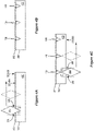
- Figure 1A illustrates a top plan view of a molded semiconductor package 100, according to an embodiment.
- Figure 1B illustrates a cross-sectional view of the molded semiconductor package 100 taken along the line labelled A-A' in Figure 1A .
- Figure 1C illustrates an enlarged view of the region labelled B in Figure 1B .
- the molded semiconductor package 100 includes semiconductor dies 102 attached to a first side 103 of a leadframe 104.
- Each semiconductor die 102 may comprise any type of semiconductor material such as Si, SiC, GaN, etc.
- Each semiconductor die 102 may include a lateral or vertical power device such as a power transistor and/or a power diode.
- a lateral power device all power and signal connections are made at the same side (e.g., facing side in Figure 1A ; top side in Figure 1B ) of the corresponding die 102.
- source, drain and gate connections may be made at the same side of the die corresponding die 102.
- some power and possibly signal connections are made at one side (e.g., the non-facing side in Figure 1A ; bottom side in Figure 1B ) of the corresponding die 102.
- the source/emitter and gate connections may be made at one side and the drain/collector connection may be made at the opposite side of the corresponding die 102.
- the semiconductor dies 102 are electrically interconnected to form a power electronic circuit such as a power converter, power inverter, B6 (3 half bridges), bridge rectifier, etc.
- the semiconductor dies 102 may be electrically interconnected to form the power electronic circuit by the leadframe 104 at the back side of the dies 102 (e.g., in the case of vertical devices) and/or by electrical conductors 106 such as wire bonds, wire ribbons, metal clips, etc. at the front side of the dies 102.
- Additional circuitry associated with operation of the power electronic circuit such as a microcontroller, driver circuitry, filters, etc. may be included in the molded semiconductor package 100, e.g., on a separate board 108 attached to the leadframe 104.
- the additional circuitry may include one or more semiconductor dies 110 and corresponding interconnects 112 such as metal traces on the board 108 and wire bonds, wire ribbons, metal clips, etc. for electrically interconnecting the one or more additional semiconductor dies 110 on the board 108 and/or electrically connecting the one or more additional semiconductor dies 110 to the semiconductor dies 102 separately attached to the leadframe 104.
- interconnects 112 such as metal traces on the board 108 and wire bonds, wire ribbons, metal clips, etc.
- a molding compound 114 encapsulates the semiconductor dies 102, 110.
- the molding compound 114 may comprise a wide variety of electrically insulating encapsulant materials including ceramics, epoxy materials and thermosetting plastics, to name a few.
- Leads 115 of the leadframe 104 may protrude through one or more side faces of the molding compound 114 to provide points of external electrical connection for the molded semiconductor package 100.
- the molding compound 114 above the leadframe 104 is not shown in Figure 1A to provide an unobstructed view of other components of the molded semiconductor package 100.
- the molded semiconductor package 100 also includes a substrate 116 attached to the side 105 of the leadframe 104 opposite the side 103 with the semiconductor dies 102.
- the substrate 116 includes a metal body 118 and an electrically insulative material 120 that separates the metal body 118 from the leadframe 104.
- the substrate 116 is thermally conductive and dissipates heat generated by the semiconductor dies 102 during operation, but the metal body 118 of the substrate 116 is electrically isolated from the semiconductor dies 102 by the electrically insulative material 120.
- the metal body 118 of the substrate 116 has a first surface 122 in contact with the electrically insulative material 120 of the substrate 116.
- the metal body 118 also has a second surface 124 opposite the first surface 122 and which is not covered by the molding compound 114.
- a bevelled edge 126 of the metal body 118 extends between the first surface 122 and the second surface 124.
- the bevelled edge 126 of the metal body 118 has a first sloped side face 128 that extends from the first surface 122 of the metal body 118 to an apex 130 of the bevelled edge 126, and a second sloped side face 132 that extends from the apex 130 of the bevelled edge 126 to the second surface 124 of the metal body 118.
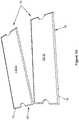
- Figure 1D includes an upper view which shows the metallized side 124 of the substrate 116, and a lower view which shows the electrically insulating side 122 of the substrate 116.
- the first sloped side face 128 of the bevelled edge 126 is visible in the lower view of Figure 1D whereas the second sloped side face 132 of the bevelled edge 126 is visible in the upper view of Figure 1D .
- the molding compound 114 contacts both the first sloped side face 128 and the second sloped side face 132 of the metal body 118 of the substrate 116, e.g., as shown in Figure 1C .
- an angle ⁇ 1 of the first sloped side face 128 of the metal body 118 of the substrate 116 as measured relative to a vertical projection from the apex 130 of the bevelled edge 126 may be in a range of 30 to 60 degrees.
- an angle a2 of the second sloped side face 132 of the metal body 118 of the substrate 116 as measured relative to a vertical projection from the apex 130 of the bevelled edge 126 may be in a range of 30 to 60 degrees.
- the metal body 118 of the substrate 116 may have a thickness 'T1' of 2 mm measured between the first and second surfaces 120, 124 of the metal body 118 and the bevelled edge 126 of the metal body 118 may have a thickness 'T2' in a range of 0.8 to 1.2 mm measured from the apex 130 inward.
- ⁇ 1 and ⁇ 2 decrease and the contact area between the molding compound 114 and the bevelled edge 126 of the substrate 116 increases which should further limit humidity penetration and increase reliability.
- a1 and a2 increase and the contact area between the molding compound 114 and the bevelled edge 126 of the substrate 116 decreases.
- a range of 30 to 60 degrees (°) for a1 and a2 provides for reduced humidity penetration and increased reliability.
- the electrically insulative material 120 of the substrate 116 may have a sloped side face 134 having the same angle ⁇ 1 as the first sloped side face 128 of the metal body 118 of the substrate 116.
- the sloped side face 134 of the electrically insulative material 120 of the substrate 116 is shown as a dashed slanted line in Figure 1C to indicate that the electrically insulative material 120 may instead have a vertical side face 136 in the bevelled edge region of the substrate 116.
- the metal body 118 of the substrate 116 may be at least 10x thicker than the electrically insulative material 120 of the substrate 116 (i.e., T1 ⁇ 10xT3 in Figure 1C ).
- T1 may be 2 mm or greater and T3 may be less than 200 ⁇ m, e.g., 160 ⁇ m or less.
- the electrically insulative material 120 of the substrate 116 may comprise one or more of SiO 2 , Al 2 O 3 , AIN, BN, and resin. Still other electrically insulating and thermally conductive materials may be used for the electrically insulative material 120 of the substrate 116.
- the metal body 118 of the substrate 116 may comprise Al, Cu or AlCu. Still other metal or metal alloys be used for the metal body 118 of the substrate 116.
- Figures 2A through 2C illustrate an embodiment of a method of producing the molded semiconductor package 100 shown in Figures 1A through 1D .
- Figure 2A shows a plan view of the semiconductor dies 102 attached to a first side 103 of the leadframe 104.
- the semiconductor dies 102 may be attached to the leadframe 104 using any standard die attach material such as solder, glue, adhesive, etc.
- the die attach material may be applied to the leadframe 104, the semiconductor dies 102, or both.
- the die attach material is not visible in Figure 2A .
- the leadframe 104 may be part of a leadframe sheet 200 that includes multiple leadframes. In this case, more than one molded semiconductor package 100 may be produced concurrently.
- FIG 2A at least some of the electrical connections 106 to the semiconductor dies 102 have been made, e.g., by wire bonding, ribbon bonding, clip bonding, etc.
- Figure 2B shows a plan view of the substrate 116 attached to the opposite side 105 of the leadframe 104 as the semiconductor dies 102.
- the substrate 116 may be attached to the leadframe 104 by bonding, gluing, adhering, soldering, etc.
- the electrically insulative material 120 of the substrate 116 electrically isolates the metal body 118 of the substrate 116 from the leadframe 104, as previously described herein.
- the electrically insulative material 120 of the substrate 116 faces upward in Figure 2B .
- the remainder of the electrical connections 106 to the semiconductor dies 102 have been made, e.g., by wire bonding, ribbon bonding, clip bonding, etc. to form the desired power electronic circuit which may include the separate board 108 with the one or more additional semiconductor dies 110.
- the separate board 108 with the one or more additional semiconductor dies 110 may be attached to the leadframe 104 by bonding, gluing, adhering, soldering, etc.
- the one or more additional semiconductor dies 110 instead may be attached directly to the leadframe 104 and the separate board 1-8 may be omitted.
- Figure 2C shows a cross-sectional view of the semiconductor dies 102 encapsulated in the molding compound 114.
- the molding compound 114 may be formed by placing the package assembly in a three-dimensional chamber and injecting liquified encapsulant material into the chamber. Examples of such techniques include injection molding, transfer molding, compression molding, and film-assist molding. In another embodiment, the molding compound 114 may be formed by a lamination technique.
- the packages 100 may be separated / singulated from one another post molding by severing the leads 115 and leadframe 104 of each molded semiconductor package 100 from the leadframe sheet 200.
- the leadframe sheet 200 may be stamped, punched, cut, etched, etc. in regions outside the molding compound 114 to singulate the packages 100.
- Figure 3A shows a bottom perspective view of a molded semiconductor package 100 produced in accordance with the method illustrated in Figures 2A through 2C , according to an embodiment.
- Figure 3B shows a top perspective view of the molded semiconductor package 100.
- Other lead types and configurations may be used.
- the second surface 124 of the metal body 118 of the substrate 116 is not covered by the molding compound 114.
- the exposed surface 124 of the metal body 118 provides an enhanced heat dissipation path at this side of the molded semiconductor package 100.
- Figures 4A through 4C illustrate partial cross-sectional views of an embodiment of a method for producing the substrate 116 used in the molded semiconductor packages 100 illustrated in Figures 1A through 3B .
- the substrate 116 Prior to attaching the substrate 116 to the leadframe 104, the substrate 116 is singulated from a substrate sheet 300.
- the substrate sheet 300 is used to concurrently produce a plurality of substrates 116 and comprises a metal or metal alloy such as Al, Cu, AlCu, etc.
- Figure 4A shows cutting a first main surface 302 of the substrate sheet 300 in multiple locations with a blade 304 having sloped sidewalls 306 to form the first sloped side face 128 of each substrate 116.
- the sloped sidewalls 306 of the blade 304 are angled ( ⁇ 1, ⁇ 2) in a range of 30 to 60 degrees.
- Figure 4B shows the substrate sheet 300 after all cuts are made in the first main surface 302 of the substrate sheet 300.
- Figure 4C shows cutting a second main surface 308 of the substrate sheet 300 in multiple locations with a blade 304 having sloped sidewalls 306 to form the second sloped side face 132 of each substrate 116.
- the sloped sidewalls 306 of the blade 304 used to cut the second main surface 308 of the substrate sheet 300 are angled ( ⁇ 1, ⁇ 2) in a range of 30 to 60 degrees.
- the same or different blade 304 may be used to cut the first and second main surfaces 302, 308 of the substrate sheet 300.
- the electrically insulative material 120 of each substrate 116 may be formed on the metal body 118 of each substrate before or after the first main surface 302 of the substrate sheet 300 is cut. Accordingly, the electrically insulative material 120 of each substrate 116 may or may not have the same sloped sidewall as the metal body 118 depending on when the electrically insulative material 120 is formed.
- the substrate sheet 300 is a composite sheet at the time of cutting and comprises a metal layer 400 and an electrically insulative layer 402 formed on a first main surface 404 of the metal layer 400.
- the first main surface 302 of the substrate sheet 300 corresponds to the main surface 406 of the electrically insulative layer 402 which faces away from the metal layer 400 as indicated by the vertical dashed arrow in Figure 4A .
- the substrate sheet 300 is cut as a metal layer 400 without the electrically insulative layer 402 formed thereon.
- the first main surface 302 of the substrate sheet 300 corresponds to the first main surface 404 of the metal layer 400 as indicated by the vertical solid arrow in Figure 4A .
- the second main surface 308 of the substrate sheet 300 corresponds to the second main surface 408 of the metal layer 400 as indicated by the vertical solid arrow in Figure 4C .
- Figures 5A through 5C illustrate partial top plan views of the substrate sheet 300 during different stages of production.
- the electrically insulative layer 402 shown in Figures 4A through 4C may be formed on the first main surface 404 of the metal layer 400 before or after cutting of the substrate sheet 300, as explained above.
- Figure 5A shows intersecting V-shaped grooves 500, 502 formed in the first main surface 404 of the metal layer 400 using the blade 304 with sloped sidewalls 306. If the electrically insulative layer 402 is formed on the first main surface 404 of the metal layer 400 before cutting of the substrate sheet 300, the intersecting V-shaped grooves 500, 502 are also formed in the electrically insulative layer 402 at the same angle as formed in the first main surface 404 of the metal layer 400.
- the angle of the intersecting V-shaped grooves 500, 502 corresponds to the angle ⁇ 1, ⁇ 2 of the sidewalls 306 of the blade 304 used to form the V-shaped grooves 500, 502 in the first main surface 404 of the metal layer 400, e.g., as shown in Figure 4A .
- Corresponding intersecting V-shaped grooves are formed in the second main surface 408 of the metal layer 400 using the same or different blade 304 with sloped sidewalls 306.
- the metal layer 400 may be cut halfway through from the first main surface 404, then the substrate sheet 300 is flipped and the cutting continues from the second main surface 408 of the metal layer 400.
- This approach results in the apex 130 of each bevelled edge 126 being approximately centered along the horizontal center line of each substrate 116.
- the apex 130 of each bevelled edge 126 instead may be formed off-centered with respect to the horizontal center line by cutting deeper into one of the main surfaces 404/408 of the substrate sheet 300 than the other surface 408/404.
- the intersecting V-shaped grooves formed in the second main surface 408 of the metal layer 400 are out of view in Figure 5A , but are vertically aligned with the intersecting V-shaped grooves 500, 502 formed in the first main surface 404 of the metal layer 400, e.g., as shown in Figure 4C .
- the V-shaped grooves may be formed in both main surfaces 404, 408 of the metal layer 400 by moving the same or different blade 304 with the same or different cutting angle in the x and y directions indicated in Figure 5A .
- Figure 5B shows openings 504 formed in the substrate sheet 300.
- the openings 504 may be used for alignment and/or fixing of the substrates 116 during subsequent processing, e.g., during molding.
- the openings 504 may be formed by punching, etching, laser drilling, mechanical drilling, etc.
- Figure 5C shows individual substrates 116 formed from the substrate sheet 300.
- the substrate sheet 300 may be stamped, punched, etched, cut, etc. to singulate the substrates 116.
- the substrates 116 are singulated along the vertically aligned V-shaped grooves formed in the opposing main surfaces 404, 408 of the metal layer 400.
- the substrate sheet 300 may be processed with the leadframe sheet 200 shown in Figures 2A through 2D with the substrates 116 singulated from the substrate sheet 300 post molding.
- the substrates 116 and leadframes 104 may be singulated using the same process, e.g., stamping, punching, etching, cutting, etc. post molding.
- the singulated substrates 116 each have the metal body 118, electrically insulative material 120 and bevelled edge 126 previously described herein.
- Example 1 A molded semiconductor package, comprising: a plurality of semiconductor dies attached to a first side of a leadframe and electrically interconnected to form a power electronic circuit; a substrate attached to a second side of the leadframe opposite the first side, the substrate comprising a metal body and an electrically insulative material that separates the metal body from the leadframe; and a molding compound encapsulating the plurality of semiconductor dies, wherein the metal body comprises: a first surface in contact with the electrically insulative material; a second surface opposite the first surface and which is not covered by the molding compound; and a bevelled edge that extends between the first surface and the second surface, wherein the bevelled edge of the metal body has a first sloped side face that extends from the first surface to an apex of the bevelled edge, and a second sloped side face that extends from the apex to the second surface.
- Example 2 The molded semiconductor package of example 1, wherein the molding compound contacts both the first sloped side face and the second sloped side face of the metal body.
- Example 3 The molded semiconductor package of example 1 or 2, wherein an angle of the first sloped side face of the metal body as measured relative to a vertical projection from the apex of the bevelled edge is in a range of 30 to 60 degrees.
- Example 4 The molded semiconductor package of any of examples 1 through 3, wherein an angle of the second sloped side face of the metal body as measured relative to a vertical projection from the apex of the bevelled edge is in a range of 30 to 60 degrees.
- Example 5 The molded semiconductor package of any of examples 1 through 4, wherein the first sloped side face and the second sloped side face of the metal body have the same slope.
- Example 6 The molded semiconductor package of any of examples 1 through 5, wherein the metal body has a thickness of 2 mm measured between the first surface and the second surface, and wherein the bevelled edge of the metal body has a thickness in a range of 0.8 to 1.2 mm measured from the apex inward.
- Example 7 The molded semiconductor package of any of examples 1 through 6, wherein the electrically insulative material has a sloped side face having the same angle as the first sloped side face of the metal body.
- Example 8 The molded semiconductor package of any of examples 1 through 7, wherein the metal body is at least 10x thicker than the electrically insulative material.
- Example 9 The molded semiconductor package of any of examples 1 through 8, wherein the electrically insulative material comprises one or more of SiO2, Al2O3, AIN, BN, and resin.
- Example 10 The molded semiconductor package of any of examples 1 through 9, wherein the metal body comprises Al, Cu or AlCu.
- Example 11 A method of producing a molded semiconductor package, the method comprising: attaching a plurality of semiconductor dies to a first side of a leadframe; electrically interconnecting the plurality of semiconductor dies to form a power electronic circuit; attaching a substrate to a second side of the leadframe opposite the first side, the substrate comprising a metal body and an electrically insulative material that separates the metal body from the leadframe; and encapsulating the plurality of semiconductor dies in a molding compound, wherein the metal body comprises: a first surface in contact with the electrically insulative material; a second surface opposite the first surface and which is not covered by the molding compound; and a bevelled edge that extends between the first surface and the second surface, wherein the bevelled edge of the metal body has a first sloped side face that extends from the first surface to an apex of the bevelled edge, and a second sloped side face that extends from the apex to the second surface.
- Example 12 The method of example 11, further comprising: prior to attaching the substrate to the second side of the leadframe, singulating the substrate from a substrate sheet.
- Example 13 The method of example 12, further comprising: prior to singulating the substrate from the substrate sheet, cutting a first main surface of the substrate sheet with a blade having sloped sidewalls to form the first sloped side face of the substrate, and cutting a second main surface of the substrate sheet opposite the first main surface with the same or different blade having sloped sidewalls to form the second sloped side face of the substrate.
- Example 14 The method of example 13, wherein the sloped sidewalls of each blade used to cut the substrate sheet are angled in a range of 30 to 60 degrees.
- Example 15 A method of batch producing molded semiconductor package substrates, the method comprising: forming an electrically insulative layer on a first main surface of a metal sheet; forming a plurality of intersecting V-shaped grooves in the first main surface of the metal sheet using a blade having sloped sidewalls; forming a plurality of intersecting V-shaped grooves in the second main surface of the metal sheet using the same or different blade having sloped sidewalls, the intersecting V-shaped grooves formed in the second main surface of the metal sheet being vertically aligned with the intersecting V-shaped grooves formed in the first main surface of the metal sheet; and singulating the molded semiconductor package substrates along the V-shaped grooves formed in the first main surface and the second main surface of the metal sheet such that each singulated molded semiconductor package substrate has a metal body and an electrically insulative material.
- the metal body of each molded semiconductor package substrate comprises: a first surface in contact with the electrically insulative material; a second surface opposite the first surface; and a bevelled edge that extends between the first surface and the second surface;
- the bevelled edge of each metal body has a first sloped side face that extends from the first surface of the metal body to an apex of the bevelled edge, and a second sloped side face that extends from the apex to the second surface of the metal body; an angle of the first sloped side face of each metal body corresponds to the angle of the sidewalls of the blade used to form the V-shaped grooves in the first main surface of the metal sheet; and an angle of the second sloped side face of each metal body corresponds to the angle of the sidewalls of the blade used to form the V-shaped grooves in the second main surface of the metal sheet.
- Example 17 The method of example 16, wherein the angle of the sloped sidewalls of the blade used to form the V-shaped grooves in the first main surface of the metal sheet is in a range of 30 to 60 degrees.
- Example 18 The method of example 16 or 17, wherein the angle of the sloped sidewalls of the blade used to form the V-shaped grooves in the second main surface of the metal sheet is in a range of 30 to 60 degrees.
- Example 19 The method of any of example 16 through 18, wherein: the electrically insulative layer is formed on the first main surface of the metal sheet before the V-shaped grooves are formed in the first main surface of the metal sheet; the electrically insulative material of each molded semiconductor package substrate has a sloped side face having the same angle as the first sloped side face of the metal body of the molded semiconductor package substrate; and an angle of the sloped side face of the electrically insulative material of each molded semiconductor package substrate corresponds to the angle of the sidewalls of the blade used to form the V-shaped grooves in the first main surface of the metal sheet.
- Example 20 The method of any of examples 15 through 19, wherein the same blade is used to form the V-shaped grooves in the both the first main surface and the second main surface of the metal sheet.
Landscapes
- Structures Or Materials For Encapsulating Or Coating Semiconductor Devices Or Solid State Devices (AREA)
Abstract
A molded semiconductor package includes: semiconductor dies attached to a first side of a leadframe and electrically interconnected to form a power electronic circuit; a substrate attached to a second side of the leadframe opposite the first side, and including a metal body and electrically insulative material that separates the metal body from the leadframe; and a molding compound encapsulating the dies. The metal body includes a first surface in contact with the electrically insulative material, a second surface opposite the first surface and which is not covered by the molding compound, and a bevelled edge extending between the first and second surfaces. The bevelled edge of the metal body has a first sloped side face that extends from the first surface to an apex of the bevelled edge, and a second sloped side face that extends from the apex to the second surface. Methods of producing the package are also described.
Description
- Molded semiconductor packages typically include a substrate for high heat dissipation under a leadframe and each semiconductor die (chip) included in the package. The substrate often includes an insulation layer on a metal layer such as copper or aluminum. The conventional edge shape of the substrate is vertically linear (straight line) or a vertical step shape with an additional cut.
- A vertically linear edge shape is prone to separate from the molding compound that encapsulates each die included in the package, allowing humidity to penetrate through the delaminated area and which leads to reduced lifetime of the molded semiconductor package.
- A vertical step shape at the substrate edge improves adherence between the substrate and molding compound, but increases the overall cost of the package by requiring an additional cutting process to make the vertical step shape during the manufacturing process.
- Accordingly, there is a need for an improved substrate design for molded semiconductor packages.
- According to an embodiment of a molded semiconductor package, the molded semiconductor package comprises: a plurality of semiconductor dies attached to a first side of a leadframe and electrically interconnected to form a power electronic circuit; a substrate attached to a second side of the leadframe opposite the first side, the substrate comprising a metal body and an electrically insulative material that separates the metal body from the leadframe; and a molding compound encapsulating the plurality of semiconductor dies, wherein the metal body comprises: a first surface in contact with the electrically insulative material; a second surface opposite the first surface and which is not covered by the molding compound; and a bevelled edge that extends between the first surface and the second surface, wherein the bevelled edge of the metal body has a first sloped side face that extends from the first surface to an apex of the bevelled edge, and a second sloped side face that extends from the apex to the second surface.
- According to an embodiment of a method of producing a molded semiconductor package, the method comprises: attaching a plurality of semiconductor dies to a first side of a leadframe; electrically interconnecting the plurality of semiconductor dies to form a power electronic circuit; attaching a substrate to a second side of the leadframe opposite the first side, the substrate comprising a metal body and an electrically insulative material that separates the metal body from the leadframe; and encapsulating the plurality of semiconductor dies in a molding compound, wherein the metal body comprises: a first surface in contact with the electrically insulative material; a second surface opposite the first surface and which is not covered by the molding compound; and a bevelled edge that extends between the first surface and the second surface, wherein the bevelled edge of the metal body has a first sloped side face that extends from the first surface to an apex of the bevelled edge, and a second sloped side face that extends from the apex to the second surface.
- According to an embodiment of a method of batch producing molded semiconductor package substrates, the method comprises: forming an electrically insulative layer on a first main surface of a metal sheet; forming a plurality of intersecting V-shaped grooves in the first main surface of the metal sheet using a blade having sloped sidewalls; forming a plurality of intersecting V-shaped grooves in the second main surface of the metal sheet using the same or different blade having sloped sidewalls, the intersecting V-shaped grooves formed in the second main surface of the metal sheet being vertically aligned with the intersecting V-shaped grooves formed in the first main surface of the metal sheet; and singulating the molded semiconductor package substrates along the V-shaped grooves formed in the first main surface and the second main surface of the metal sheet such that each singulated molded semiconductor package substrate has a metal body and an electrically insulative material.
- Those skilled in the art will recognize additional features and advantages upon reading the following detailed description, and upon viewing the accompanying drawings.
- The elements of the drawings are not necessarily to scale relative to each other. Like reference numerals designate corresponding similar parts. The features of the various illustrated embodiments can be combined unless they exclude each other. Embodiments are depicted in the drawings and are detailed in the description which follows.
-
Figure 1A illustrates a top plan view of a molded semiconductor package, according to an embodiment. -
Figure 1B illustrates a cross-sectional view of the molded semiconductor package taken along the line labelled A-A' inFigure 1A . -
Figure 1C illustrates an enlarged view of the region labelled B inFigure 1B . -
Figure 1D illustrates a metallized side and an electrically insulating side of a substrate included in the molded semiconductor package. -
Figures 2A through 2C illustrate an embodiment of a method of producing the molded semiconductor package shown inFigures 1A through 1D . -
Figure 3A shows a bottom perspective view of a molded semiconductor package produced in accordance with the method illustrated inFigures 2A through 2C , according to an embodiment. -
Figure 3B shows a top perspective view of the molded semiconductor package shown inFigure 3A . -
Figures 4A through 4C illustrate partial cross-sectional views of an embodiment of a method for producing the substrate used in the molded semiconductor packages shown inFigures 1A through 3B . -
Figures 5A through 5C illustrate partial top plan views of a substrate sheet used to produce the package substrates shown inFigures 1A through 4C , during different stages of production. - The embodiments described herein provide a molded semiconductor package having a heat dissipation substrate with a bevelled edge. The substrate with the bevelled edge is attached to a heat dissipation side of a leadframe, with semiconductor dies being attached to the opposite side of the leadframe. The bevelled edge of the substrate provides enhanced adherence between the substrate and a molding compound that encapsulates the dies as compared to a vertical linear edge, and offers higher thermal performance with larger exposed metal layer compared to a step cut edge shape.
- Described next, with reference to the figures, are exemplary embodiments of the molded semiconductor package and related methods of production.
-
Figure 1A illustrates a top plan view of a moldedsemiconductor package 100, according to an embodiment.Figure 1B illustrates a cross-sectional view of themolded semiconductor package 100 taken along the line labelled A-A' inFigure 1A .Figure 1C illustrates an enlarged view of the region labelled B inFigure 1B . - The
molded semiconductor package 100 includes semiconductor dies 102 attached to afirst side 103 of aleadframe 104. Each semiconductor die 102 may comprise any type of semiconductor material such as Si, SiC, GaN, etc. Eachsemiconductor die 102 may include a lateral or vertical power device such as a power transistor and/or a power diode. In the case of a lateral power device, all power and signal connections are made at the same side (e.g., facing side inFigure 1A ; top side inFigure 1B ) of thecorresponding die 102. For example, in the case of a lateral GaN power HEMT (high-electron-mobility transistor), source, drain and gate connections may be made at the same side of thedie corresponding die 102. In the case of a vertical power device, some power and possibly signal connections are made at one side (e.g., the non-facing side inFigure 1A ; bottom side inFigure 1B ) of thecorresponding die 102. For example, in the case of a vertical power MOSFET (metal-oxide-semiconductor field-effect transistor) or vertical IGBT (insulated gate bipolar transistor), the source/emitter and gate connections may be made at one side and the drain/collector connection may be made at the opposite side of thecorresponding die 102. - The semiconductor dies 102 are electrically interconnected to form a power electronic circuit such as a power converter, power inverter, B6 (3 half bridges), bridge rectifier, etc. The semiconductor dies 102 may be electrically interconnected to form the power electronic circuit by the
leadframe 104 at the back side of the dies 102 (e.g., in the case of vertical devices) and/or byelectrical conductors 106 such as wire bonds, wire ribbons, metal clips, etc. at the front side of thedies 102. Additional circuitry associated with operation of the power electronic circuit such as a microcontroller, driver circuitry, filters, etc. may be included in themolded semiconductor package 100, e.g., on aseparate board 108 attached to theleadframe 104. The additional circuitry may include one or more semiconductor dies 110 andcorresponding interconnects 112 such as metal traces on theboard 108 and wire bonds, wire ribbons, metal clips, etc. for electrically interconnecting the one or more additional semiconductor dies 110 on theboard 108 and/or electrically connecting the one or more additional semiconductor dies 110 to the semiconductor dies 102 separately attached to theleadframe 104. - A
molding compound 114 encapsulates the semiconductor dies 102, 110. Themolding compound 114 may comprise a wide variety of electrically insulating encapsulant materials including ceramics, epoxy materials and thermosetting plastics, to name a few.Leads 115 of theleadframe 104 may protrude through one or more side faces of themolding compound 114 to provide points of external electrical connection for the moldedsemiconductor package 100. Themolding compound 114 above theleadframe 104 is not shown inFigure 1A to provide an unobstructed view of other components of the moldedsemiconductor package 100. - The molded
semiconductor package 100 also includes asubstrate 116 attached to theside 105 of theleadframe 104 opposite theside 103 with the semiconductor dies 102. Thesubstrate 116 includes ametal body 118 and an electricallyinsulative material 120 that separates themetal body 118 from theleadframe 104. Thesubstrate 116 is thermally conductive and dissipates heat generated by the semiconductor dies 102 during operation, but themetal body 118 of thesubstrate 116 is electrically isolated from the semiconductor dies 102 by the electricallyinsulative material 120. - As shown in the enlarged view of
Figure 1C , themetal body 118 of thesubstrate 116 has afirst surface 122 in contact with the electricallyinsulative material 120 of thesubstrate 116. Themetal body 118 also has asecond surface 124 opposite thefirst surface 122 and which is not covered by themolding compound 114. Abevelled edge 126 of themetal body 118 extends between thefirst surface 122 and thesecond surface 124. Thebevelled edge 126 of themetal body 118 has a first slopedside face 128 that extends from thefirst surface 122 of themetal body 118 to anapex 130 of thebevelled edge 126, and a second slopedside face 132 that extends from theapex 130 of thebevelled edge 126 to thesecond surface 124 of themetal body 118. -
Figure 1D includes an upper view which shows themetallized side 124 of thesubstrate 116, and a lower view which shows the electrically insulatingside 122 of thesubstrate 116. The first slopedside face 128 of thebevelled edge 126 is visible in the lower view ofFigure 1D whereas the second slopedside face 132 of thebevelled edge 126 is visible in the upper view ofFigure 1D . - In one embodiment, the
molding compound 114 contacts both the first slopedside face 128 and the second slopedside face 132 of themetal body 118 of thesubstrate 116, e.g., as shown inFigure 1C . - Separately or in combination, an angle α1 of the first sloped
side face 128 of themetal body 118 of thesubstrate 116 as measured relative to a vertical projection from theapex 130 of thebevelled edge 126 may be in a range of 30 to 60 degrees. - Separately or in combination, an angle a2 of the second sloped
side face 132 of themetal body 118 of thesubstrate 116 as measured relative to a vertical projection from theapex 130 of thebevelled edge 126 may be in a range of 30 to 60 degrees. - Separately or in combination, the first sloped
side face 128 and the second slopedside face 132 of themetal body 118 of thesubstrate 116 may have the same slope (i.e., a1 = a2 inFigure 1C ). - Separately or in combination, the
metal body 118 of thesubstrate 116 may have a thickness 'T1' of 2 mm measured between the first andsecond surfaces metal body 118 and thebevelled edge 126 of themetal body 118 may have a thickness 'T2' in a range of 0.8 to 1.2 mm measured from theapex 130 inward. For T1 = 2 mm and T2 = 1 mm, a1 = a2 = 45°. For the same T1 but a larger T2 (e.g., 1.2 mm), α1 and α2 decrease and the contact area between themolding compound 114 and thebevelled edge 126 of thesubstrate 116 increases which should further limit humidity penetration and increase reliability. For the same T1 but a smaller T2 (e.g., 0.8 mm), a1 and a2 increase and the contact area between themolding compound 114 and thebevelled edge 126 of thesubstrate 116 decreases. A range of 30 to 60 degrees (°) for a1 and a2 provides for reduced humidity penetration and increased reliability. - Separately or in combination, the electrically
insulative material 120 of thesubstrate 116 may have a slopedside face 134 having the same angle α1 as the firstsloped side face 128 of themetal body 118 of thesubstrate 116. The slopedside face 134 of theelectrically insulative material 120 of thesubstrate 116 is shown as a dashed slanted line inFigure 1C to indicate that the electricallyinsulative material 120 may instead have avertical side face 136 in the bevelled edge region of thesubstrate 116. - Separately or in combination, the
metal body 118 of thesubstrate 116 may be at least 10x thicker than theelectrically insulative material 120 of the substrate 116 (i.e., T1 ≥ 10xT3 inFigure 1C ). For example, T1 may be 2 mm or greater and T3 may be less than 200 µm, e.g., 160 µm or less. - Separately or in combination, the electrically
insulative material 120 of thesubstrate 116 may comprise one or more of SiO2, Al2O3, AIN, BN, and resin. Still other electrically insulating and thermally conductive materials may be used for theelectrically insulative material 120 of thesubstrate 116. - Separately or in combination, the
metal body 118 of thesubstrate 116 may comprise Al, Cu or AlCu. Still other metal or metal alloys be used for themetal body 118 of thesubstrate 116. -
Figures 2A through 2C illustrate an embodiment of a method of producing the moldedsemiconductor package 100 shown inFigures 1A through 1D . -
Figure 2A shows a plan view of the semiconductor dies 102 attached to afirst side 103 of theleadframe 104. The semiconductor dies 102 may be attached to theleadframe 104 using any standard die attach material such as solder, glue, adhesive, etc. The die attach material may be applied to theleadframe 104, the semiconductor dies 102, or both. The die attach material is not visible inFigure 2A . - The
leadframe 104 may be part of aleadframe sheet 200 that includes multiple leadframes. In this case, more than one moldedsemiconductor package 100 may be produced concurrently. InFigure 2A , at least some of theelectrical connections 106 to the semiconductor dies 102 have been made, e.g., by wire bonding, ribbon bonding, clip bonding, etc. -
Figure 2B shows a plan view of thesubstrate 116 attached to theopposite side 105 of theleadframe 104 as the semiconductor dies 102. Thesubstrate 116 may be attached to theleadframe 104 by bonding, gluing, adhering, soldering, etc. Theelectrically insulative material 120 of thesubstrate 116 electrically isolates themetal body 118 of thesubstrate 116 from theleadframe 104, as previously described herein. Theelectrically insulative material 120 of thesubstrate 116 faces upward inFigure 2B . - Further in
Figure 2B , the remainder of theelectrical connections 106 to the semiconductor dies 102 have been made, e.g., by wire bonding, ribbon bonding, clip bonding, etc. to form the desired power electronic circuit which may include theseparate board 108 with the one or more additional semiconductor dies 110. Theseparate board 108 with the one or more additional semiconductor dies 110 may be attached to theleadframe 104 by bonding, gluing, adhering, soldering, etc. The one or more additional semiconductor dies 110 instead may be attached directly to theleadframe 104 and the separate board 1-8 may be omitted. -
Figure 2C shows a cross-sectional view of the semiconductor dies 102 encapsulated in themolding compound 114. Themolding compound 114 may be formed by placing the package assembly in a three-dimensional chamber and injecting liquified encapsulant material into the chamber. Examples of such techniques include injection molding, transfer molding, compression molding, and film-assist molding. In another embodiment, themolding compound 114 may be formed by a lamination technique. - In the case of batch producing the molded
semiconductor packages 100 using aleadframe sheet 200, thepackages 100 may be separated / singulated from one another post molding by severing theleads 115 andleadframe 104 of each moldedsemiconductor package 100 from theleadframe sheet 200. For example, theleadframe sheet 200 may be stamped, punched, cut, etched, etc. in regions outside themolding compound 114 to singulate thepackages 100. -
Figure 3A shows a bottom perspective view of a moldedsemiconductor package 100 produced in accordance with the method illustrated inFigures 2A through 2C , according to an embodiment.Figure 3B shows a top perspective view of the moldedsemiconductor package 100. Other lead types and configurations may be used. In each case, thesecond surface 124 of themetal body 118 of thesubstrate 116 is not covered by themolding compound 114. The exposedsurface 124 of themetal body 118 provides an enhanced heat dissipation path at this side of the moldedsemiconductor package 100. -
Figures 4A through 4C illustrate partial cross-sectional views of an embodiment of a method for producing thesubstrate 116 used in the moldedsemiconductor packages 100 illustrated inFigures 1A through 3B . Prior to attaching thesubstrate 116 to theleadframe 104, thesubstrate 116 is singulated from asubstrate sheet 300. Thesubstrate sheet 300 is used to concurrently produce a plurality ofsubstrates 116 and comprises a metal or metal alloy such as Al, Cu, AlCu, etc. -
Figure 4A shows cutting a first main surface 302 of thesubstrate sheet 300 in multiple locations with ablade 304 having slopedsidewalls 306 to form the firstsloped side face 128 of eachsubstrate 116. In one embodiment, the sloped sidewalls 306 of theblade 304 are angled (β1, β2) in a range of 30 to 60 degrees. -
Figure 4B shows thesubstrate sheet 300 after all cuts are made in the first main surface 302 of thesubstrate sheet 300. -
Figure 4C shows cutting a second main surface 308 of thesubstrate sheet 300 in multiple locations with ablade 304 having slopedsidewalls 306 to form the secondsloped side face 132 of eachsubstrate 116. In one embodiment, the sloped sidewalls 306 of theblade 304 used to cut the second main surface 308 of thesubstrate sheet 300 are angled (β1, β2) in a range of 30 to 60 degrees. - The same or
different blade 304 may be used to cut the first and second main surfaces 302, 308 of thesubstrate sheet 300. In the case of thesame blade 304 being used, the first and second sloped side faces 128, 132 of eachsubstrate 116 have the same angle (a1 = a2 = β1 = β2). Ifdifferent blades 304 are used to cut the first and second main surfaces 302, 308 of thesubstrate sheet 300, the first and second sloped side faces 128, 132 of eachsubstrate 116 may have different angles if the sidewalls slopes for theblades 304 are different (e.g., α1 = α2 ≠ β1 = β2). - The
electrically insulative material 120 of eachsubstrate 116 may be formed on themetal body 118 of each substrate before or after the first main surface 302 of thesubstrate sheet 300 is cut. Accordingly, the electricallyinsulative material 120 of eachsubstrate 116 may or may not have the same sloped sidewall as themetal body 118 depending on when the electricallyinsulative material 120 is formed. - In one embodiment, the
substrate sheet 300 is a composite sheet at the time of cutting and comprises ametal layer 400 and an electricallyinsulative layer 402 formed on a first main surface 404 of themetal layer 400. According to this embodiment, the first main surface 302 of thesubstrate sheet 300 corresponds to the main surface 406 of theelectrically insulative layer 402 which faces away from themetal layer 400 as indicated by the vertical dashed arrow inFigure 4A . - In another embodiment, the
substrate sheet 300 is cut as ametal layer 400 without theelectrically insulative layer 402 formed thereon. According to this embodiment, the first main surface 302 of thesubstrate sheet 300 corresponds to the first main surface 404 of themetal layer 400 as indicated by the vertical solid arrow inFigure 4A . In either case, the second main surface 308 of thesubstrate sheet 300 corresponds to the second main surface 408 of themetal layer 400 as indicated by the vertical solid arrow inFigure 4C . -
Figures 5A through 5C illustrate partial top plan views of thesubstrate sheet 300 during different stages of production. Theelectrically insulative layer 402 shown inFigures 4A through 4C may be formed on the first main surface 404 of themetal layer 400 before or after cutting of thesubstrate sheet 300, as explained above. -
Figure 5A shows intersecting V-shapedgrooves metal layer 400 using theblade 304 with slopedsidewalls 306. If theelectrically insulative layer 402 is formed on the first main surface 404 of themetal layer 400 before cutting of thesubstrate sheet 300, the intersecting V-shapedgrooves electrically insulative layer 402 at the same angle as formed in the first main surface 404 of themetal layer 400. The angle of the intersecting V-shapedgrooves sidewalls 306 of theblade 304 used to form the V-shapedgrooves metal layer 400, e.g., as shown inFigure 4A . - Corresponding intersecting V-shaped grooves are formed in the second main surface 408 of the
metal layer 400 using the same ordifferent blade 304 with slopedsidewalls 306. For example, themetal layer 400 may be cut halfway through from the first main surface 404, then thesubstrate sheet 300 is flipped and the cutting continues from the second main surface 408 of themetal layer 400. This approach results in the apex 130 of eachbevelled edge 126 being approximately centered along the horizontal center line of eachsubstrate 116. The apex 130 of eachbevelled edge 126 instead may be formed off-centered with respect to the horizontal center line by cutting deeper into one of the main surfaces 404/408 of thesubstrate sheet 300 than the other surface 408/404. - The intersecting V-shaped grooves formed in the second main surface 408 of the
metal layer 400 are out of view inFigure 5A , but are vertically aligned with the intersecting V-shapedgrooves metal layer 400, e.g., as shown inFigure 4C . The V-shaped grooves may be formed in both main surfaces 404, 408 of themetal layer 400 by moving the same ordifferent blade 304 with the same or different cutting angle in the x and y directions indicated inFigure 5A . -
Figure 5B showsopenings 504 formed in thesubstrate sheet 300. Theopenings 504 may be used for alignment and/or fixing of thesubstrates 116 during subsequent processing, e.g., during molding. Theopenings 504 may be formed by punching, etching, laser drilling, mechanical drilling, etc. -
Figure 5C showsindividual substrates 116 formed from thesubstrate sheet 300. Thesubstrate sheet 300 may be stamped, punched, etched, cut, etc. to singulate thesubstrates 116. Thesubstrates 116 are singulated along the vertically aligned V-shaped grooves formed in the opposing main surfaces 404, 408 of themetal layer 400. - Alternatively, the
substrate sheet 300 may be processed with theleadframe sheet 200 shown inFigures 2A through 2D with thesubstrates 116 singulated from thesubstrate sheet 300 post molding. For example, thesubstrates 116 andleadframes 104 may be singulated using the same process, e.g., stamping, punching, etching, cutting, etc. post molding. In each case, thesingulated substrates 116 each have themetal body 118, electricallyinsulative material 120 andbevelled edge 126 previously described herein. - Although the present disclosure is not so limited, the following numbered examples demonstrate one or more aspects of the disclosure.
- Example 1. A molded semiconductor package, comprising: a plurality of semiconductor dies attached to a first side of a leadframe and electrically interconnected to form a power electronic circuit; a substrate attached to a second side of the leadframe opposite the first side, the substrate comprising a metal body and an electrically insulative material that separates the metal body from the leadframe; and a molding compound encapsulating the plurality of semiconductor dies, wherein the metal body comprises: a first surface in contact with the electrically insulative material; a second surface opposite the first surface and which is not covered by the molding compound; and a bevelled edge that extends between the first surface and the second surface, wherein the bevelled edge of the metal body has a first sloped side face that extends from the first surface to an apex of the bevelled edge, and a second sloped side face that extends from the apex to the second surface.
- Example 2. The molded semiconductor package of example 1, wherein the molding compound contacts both the first sloped side face and the second sloped side face of the metal body.
- Example 3. The molded semiconductor package of example 1 or 2, wherein an angle of the first sloped side face of the metal body as measured relative to a vertical projection from the apex of the bevelled edge is in a range of 30 to 60 degrees.
- Example 4. The molded semiconductor package of any of examples 1 through 3, wherein an angle of the second sloped side face of the metal body as measured relative to a vertical projection from the apex of the bevelled edge is in a range of 30 to 60 degrees.
- Example 5. The molded semiconductor package of any of examples 1 through 4, wherein the first sloped side face and the second sloped side face of the metal body have the same slope.
- Example 6. The molded semiconductor package of any of examples 1 through 5, wherein the metal body has a thickness of 2 mm measured between the first surface and the second surface, and wherein the bevelled edge of the metal body has a thickness in a range of 0.8 to 1.2 mm measured from the apex inward.
- Example 7. The molded semiconductor package of any of examples 1 through 6, wherein the electrically insulative material has a sloped side face having the same angle as the first sloped side face of the metal body.
- Example 8. The molded semiconductor package of any of examples 1 through 7, wherein the metal body is at least 10x thicker than the electrically insulative material.
- Example 9. The molded semiconductor package of any of examples 1 through 8, wherein the electrically insulative material comprises one or more of SiO2, Al2O3, AIN, BN, and resin.
- Example 10. The molded semiconductor package of any of examples 1 through 9, wherein the metal body comprises Al, Cu or AlCu.
- Example 11. A method of producing a molded semiconductor package, the method comprising: attaching a plurality of semiconductor dies to a first side of a leadframe; electrically interconnecting the plurality of semiconductor dies to form a power electronic circuit; attaching a substrate to a second side of the leadframe opposite the first side, the substrate comprising a metal body and an electrically insulative material that separates the metal body from the leadframe; and encapsulating the plurality of semiconductor dies in a molding compound, wherein the metal body comprises: a first surface in contact with the electrically insulative material; a second surface opposite the first surface and which is not covered by the molding compound; and a bevelled edge that extends between the first surface and the second surface, wherein the bevelled edge of the metal body has a first sloped side face that extends from the first surface to an apex of the bevelled edge, and a second sloped side face that extends from the apex to the second surface.
- Example 12. The method of example 11, further comprising: prior to attaching the substrate to the second side of the leadframe, singulating the substrate from a substrate sheet.
- Example 13. The method of example 12, further comprising: prior to singulating the substrate from the substrate sheet, cutting a first main surface of the substrate sheet with a blade having sloped sidewalls to form the first sloped side face of the substrate, and cutting a second main surface of the substrate sheet opposite the first main surface with the same or different blade having sloped sidewalls to form the second sloped side face of the substrate.
- Example 14. The method of example 13, wherein the sloped sidewalls of each blade used to cut the substrate sheet are angled in a range of 30 to 60 degrees.
- Example 15. A method of batch producing molded semiconductor package substrates, the method comprising: forming an electrically insulative layer on a first main surface of a metal sheet; forming a plurality of intersecting V-shaped grooves in the first main surface of the metal sheet using a blade having sloped sidewalls; forming a plurality of intersecting V-shaped grooves in the second main surface of the metal sheet using the same or different blade having sloped sidewalls, the intersecting V-shaped grooves formed in the second main surface of the metal sheet being vertically aligned with the intersecting V-shaped grooves formed in the first main surface of the metal sheet; and singulating the molded semiconductor package substrates along the V-shaped grooves formed in the first main surface and the second main surface of the metal sheet such that each singulated molded semiconductor package substrate has a metal body and an electrically insulative material.
- The method of example 15, wherein: the metal body of each molded semiconductor package substrate comprises: a first surface in contact with the electrically insulative material; a second surface opposite the first surface; and a bevelled edge that extends between the first surface and the second surface; the bevelled edge of each metal body has a first sloped side face that extends from the first surface of the metal body to an apex of the bevelled edge, and a second sloped side face that extends from the apex to the second surface of the metal body; an angle of the first sloped side face of each metal body corresponds to the angle of the sidewalls of the blade used to form the V-shaped grooves in the first main surface of the metal sheet; and an angle of the second sloped side face of each metal body corresponds to the angle of the sidewalls of the blade used to form the V-shaped grooves in the second main surface of the metal sheet.
- Example 17. The method of example 16, wherein the angle of the sloped sidewalls of the blade used to form the V-shaped grooves in the first main surface of the metal sheet is in a range of 30 to 60 degrees.
- Example 18. The method of example 16 or 17, wherein the angle of the sloped sidewalls of the blade used to form the V-shaped grooves in the second main surface of the metal sheet is in a range of 30 to 60 degrees.
- Example 19. The method of any of example 16 through 18, wherein: the electrically insulative layer is formed on the first main surface of the metal sheet before the V-shaped grooves are formed in the first main surface of the metal sheet; the electrically insulative material of each molded semiconductor package substrate has a sloped side face having the same angle as the first sloped side face of the metal body of the molded semiconductor package substrate; and an angle of the sloped side face of the electrically insulative material of each molded semiconductor package substrate corresponds to the angle of the sidewalls of the blade used to form the V-shaped grooves in the first main surface of the metal sheet.
- Example 20. The method of any of examples 15 through 19, wherein the same blade is used to form the V-shaped grooves in the both the first main surface and the second main surface of the metal sheet.
- Terms such as "first", "second", and the like, are used to describe various elements, regions, sections, etc. and are also not intended to be limiting. Like terms refer to like elements throughout the description.
- As used herein, the terms "having", "containing", "including", "comprising" and the like are open ended terms that indicate the presence of stated elements or features, but do not preclude additional elements or features. The articles "a", "an" and "the" are intended to include the plural as well as the singular, unless the context clearly indicates otherwise.
- It is to be understood that the features of the various embodiments described herein may be combined with each other, unless specifically noted otherwise.
- Although specific embodiments have been illustrated and described herein, it will be appreciated by those of ordinary skill in the art that a variety of alternate and/or equivalent implementations may be substituted for the specific embodiments shown and described without departing from the scope of the present invention. This application is intended to cover any adaptations or variations of the specific embodiments discussed herein. Therefore, it is intended that this invention be limited only by the claims and the equivalents thereof.
Claims (15)
- A molded semiconductor package, comprising:a plurality of semiconductor dies attached to a first side of a leadframe and electrically interconnected to form a power electronic circuit;a substrate attached to a second side of the leadframe opposite the first side, the substrate comprising a metal body and an electrically insulative material that separates the metal body from the leadframe; anda molding compound encapsulating the plurality of semiconductor dies,wherein the metal body comprises:a first surface in contact with the electrically insulative material;a second surface opposite the first surface and which is not covered by the molding compound; anda bevelled edge that extends between the first surface and the second surface, wherein the bevelled edge of the metal body has a first sloped side face that extendsfrom the first surface to an apex of the bevelled edge, and a second sloped side face that extends from the apex to the second surface.
- The molded semiconductor package of claim 1, wherein the molding compound contacts both the first sloped side face and the second sloped side face of the metal body.
- The molded semiconductor package of claim 1 or 2, wherein an angle of the first sloped side face of the metal body as measured relative to a vertical projection from the apex of the bevelled edge is in a range of 30 to 60 degrees, and
wherein an angle of the second sloped side face of the metal body as measured relative to a vertical projection from the apex of the bevelled edge is in a range of 30 to 60 degrees. - The molded semiconductor package of one of the preceding claims, wherein the metal body has a thickness of 2 mm measured between the first surface and the second surface, and wherein the bevelled edge of the metal body has a thickness in a range of 0.8 to 1.2 mm measured from the apex inward.
- The molded semiconductor package of one of the preceding claims, wherein the electrically insulative material has a sloped side face having the same angle as the first sloped side face of the metal body.
- The molded semiconductor package of one of the preceding claims, wherein the metal body is at least 10x thicker than the electrically insulative material.
- The molded semiconductor package of one of the preceding claims, wherein the electrically insulative material comprises one or more of SiO2, Al2O3, AIN, BN, and resin.
- A method of producing a molded semiconductor package, the method comprising:attaching a plurality of semiconductor dies to a first side of a leadframe;electrically interconnecting the plurality of semiconductor dies to form a power electronic circuit;attaching a substrate to a second side of the leadframe opposite the first side, the substrate comprising a metal body and an electrically insulative material that separates the metal body from the leadframe; andencapsulating the plurality of semiconductor dies in a molding compound,wherein the metal body comprises:a first surface in contact with the electrically insulative material;a second surface opposite the first surface and which is not covered by the molding compound; anda bevelled edge that extends between the first surface and the second surface, wherein the bevelled edge of the metal body has a first sloped side face that extendsfrom the first surface to an apex of the bevelled edge, and a second sloped side face that extends from the apex to the second surface.
- The method of claim 8, further comprising:
prior to attaching the substrate to the second side of the leadframe, singulating the substrate from a substrate sheet. - The method of claim 9, further comprising:
prior to singulating the substrate from the substrate sheet, cutting a first main surface of the substrate sheet with a blade having sloped sidewalls to form the first sloped side face of the substrate, and cutting a second main surface of the substrate sheet opposite the first main surface with the same or different blade having sloped sidewalls to form the second sloped side face of the substrate. - A method of batch producing molded semiconductor package substrates, the method comprising:forming an electrically insulative layer on a first main surface of a metal sheet;forming a plurality of intersecting V-shaped grooves in the first main surface of the metal sheet using a blade having sloped sidewalls;forming a plurality of intersecting V-shaped grooves in the second main surface of the metal sheet using the same or different blade having sloped sidewalls, the intersecting V-shaped grooves formed in the second main surface of the metal sheet being vertically aligned with the intersecting V-shaped grooves formed in the first main surface of the metal sheet; andsingulating the molded semiconductor package substrates along the V-shaped grooves formed in the first main surface and the second main surface of the metal sheet such that each singulated molded semiconductor package substrate has a metal body and an electrically insulative material.
- The method of claim 11, wherein:the metal body of each molded semiconductor package substrate comprises:a first surface in contact with the electrically insulative material;a second surface opposite the first surface; anda bevelled edge that extends between the first surface and the second surface;the bevelled edge of each metal body has a first sloped side face that extends from the first surface of the metal body to an apex of the bevelled edge, and a second sloped side face that extends from the apex to the second surface of the metal body;an angle of the first sloped side face of each metal body corresponds to the angle of the sidewalls of the blade used to form the V-shaped grooves in the first main surface of the metal sheet; andan angle of the second sloped side face of each metal body corresponds to the angle of the sidewalls of the blade used to form the V-shaped grooves in the second main surface of the metal sheet.
- The method of claim 12, wherein the angle of the sloped sidewalls of the blade used to form the V-shaped grooves in the first main surface of the metal sheet and in the second main surface of the metal sheet is in a range of 30 to 60 degrees.
- The method of claim 12 or 13, wherein:the electrically insulative layer is formed on the first main surface of the metal sheet before the V-shaped grooves are formed in the first main surface of the metal sheet;the electrically insulative material of each molded semiconductor package substrate has a sloped side face having the same angle as the first sloped side face of the metal body of the molded semiconductor package substrate; andan angle of the sloped side face of the electrically insulative material of each molded semiconductor package substrate corresponds to the angle of the sidewalls of the blade used to form the V-shaped grooves in the first main surface of the metal sheet.
- The method of claim one of claims 11 to 14, wherein the same blade is used to form the V-shaped grooves in the both the first main surface and the second main surface of the metal sheet.
Applications Claiming Priority (1)
| Application Number | Priority Date | Filing Date | Title |
|---|---|---|---|
| US17/193,737 US11848243B2 (en) | 2021-03-05 | 2021-03-05 | Molded semiconductor package having a substrate with bevelled edge |
Publications (1)
| Publication Number | Publication Date |
|---|---|
| EP4057336A1 true EP4057336A1 (en) | 2022-09-14 |
Family
ID=80595357
Family Applications (1)
| Application Number | Title | Priority Date | Filing Date |
|---|---|---|---|
| EP22159142.3A Withdrawn EP4057336A1 (en) | 2021-03-05 | 2022-02-28 | Molded semiconductor package having a substrate with bevelled edge |
Country Status (3)
| Country | Link |
|---|---|
| US (1) | US11848243B2 (en) |
| EP (1) | EP4057336A1 (en) |
| CN (1) | CN115020366A (en) |
Citations (5)
| Publication number | Priority date | Publication date | Assignee | Title |
|---|---|---|---|---|
| US20030057573A1 (en) * | 2001-09-26 | 2003-03-27 | Kabushiki Kaisha Toshiba | Semiconductor device |
| US20050176175A1 (en) * | 2003-12-24 | 2005-08-11 | Sanyo Electric Co., Ltd. | Method of manufacturing hybrid integrated circuit device |
| US20070187839A1 (en) * | 2006-02-16 | 2007-08-16 | Stats Chippac Ltd. | Integrated circuit package system with heat sink |
| JP2010219385A (en) * | 2009-03-18 | 2010-09-30 | Mitsubishi Electric Corp | Semiconductor device |
| US20150371921A1 (en) * | 2013-02-05 | 2015-12-24 | Panasonic Intellectual Property Management Co., Ltd. | Semiconductor device and method for manufacturing same |
Family Cites Families (6)
| Publication number | Priority date | Publication date | Assignee | Title |
|---|---|---|---|---|
| US5196378A (en) | 1987-12-17 | 1993-03-23 | Texas Instruments Incorporated | Method of fabricating an integrated circuit having active regions near a die edge |
| US7232957B2 (en) * | 2003-09-25 | 2007-06-19 | Sanyo Electric Co., Ltd. | Hybrid integrated circuit device and method of manufacturing the same |
| JP4158738B2 (en) | 2004-04-20 | 2008-10-01 | 株式会社デンソー | Semiconductor module mounting structure, card-like semiconductor module, and heat-receiving member for adhering to card-like semiconductor module |
| KR100765945B1 (en) | 2004-08-06 | 2007-10-10 | 가부시끼가이샤 아라이도 마테리아루 | Collective substrate, semiconductor element mounting member, semiconductor device, imaging device, light emitting diode constituting member, and light emitting diode |
| JP2014093365A (en) | 2012-11-01 | 2014-05-19 | Toyota Industries Corp | Semiconductor device |
| WO2016120997A1 (en) | 2015-01-27 | 2016-08-04 | 三菱電機株式会社 | Semiconductor module |
-
2021
- 2021-03-05 US US17/193,737 patent/US11848243B2/en active Active
-
2022
- 2022-02-28 EP EP22159142.3A patent/EP4057336A1/en not_active Withdrawn
- 2022-03-04 CN CN202210207262.XA patent/CN115020366A/en active Pending
Patent Citations (5)
| Publication number | Priority date | Publication date | Assignee | Title |
|---|---|---|---|---|
| US20030057573A1 (en) * | 2001-09-26 | 2003-03-27 | Kabushiki Kaisha Toshiba | Semiconductor device |
| US20050176175A1 (en) * | 2003-12-24 | 2005-08-11 | Sanyo Electric Co., Ltd. | Method of manufacturing hybrid integrated circuit device |
| US20070187839A1 (en) * | 2006-02-16 | 2007-08-16 | Stats Chippac Ltd. | Integrated circuit package system with heat sink |
| JP2010219385A (en) * | 2009-03-18 | 2010-09-30 | Mitsubishi Electric Corp | Semiconductor device |
| US20150371921A1 (en) * | 2013-02-05 | 2015-12-24 | Panasonic Intellectual Property Management Co., Ltd. | Semiconductor device and method for manufacturing same |
Also Published As
| Publication number | Publication date |
|---|---|
| US11848243B2 (en) | 2023-12-19 |
| US20220285239A1 (en) | 2022-09-08 |
| CN115020366A (en) | 2022-09-06 |
Similar Documents
| Publication | Publication Date | Title |
|---|---|---|
| US7582958B2 (en) | Semiconductor package | |
| US7042068B2 (en) | Leadframe and semiconductor package made using the leadframe | |
| US6784540B2 (en) | Semiconductor device package with improved cooling | |
| EP2605276B1 (en) | Packaged leadless semiconductor device | |
| US7732899B1 (en) | Etch singulated semiconductor package | |
| US6756658B1 (en) | Making two lead surface mounting high power microleadframe semiconductor packages | |
| CN101364548B (en) | Method of manufacturing an integrated circuit module | |
| US7084488B2 (en) | Packaged semiconductor device and method of manufacture using shaped die | |
| US12368126B2 (en) | High thermal dissipation, packaged electronic device and manufacturing process thereof | |
| US20080290487A1 (en) | Lead frame for semiconductor device | |
| CN104064529B (en) | The method of semiconductor devices, semiconductor module and manufacture semiconductor devices and semiconductor module | |
| JP6709785B2 (en) | Package for electronic system having semiconductor chip | |
| US9355942B2 (en) | Gang clips having distributed-function tie bars | |
| US11145578B2 (en) | Semiconductor package with top or bottom side cooling and method for manufacturing the semiconductor package | |
| CN111244061B (en) | Packaging structure of GaN devices | |
| US6576988B2 (en) | Semiconductor package | |
| US11450593B2 (en) | Spacer frame for semiconductor packages | |
| US11848243B2 (en) | Molded semiconductor package having a substrate with bevelled edge | |
| US20240258372A1 (en) | Electronic component and package including stress release structure as lateral edge portion of semiconductor body | |
| CN117790434A (en) | A package with an electrically insulating and thermally conductive layer on top of an electronic component | |
| US6284570B1 (en) | Method of manufacturing a semiconductor component from a conductive substrate containing a plurality of vias | |
| US20250226297A1 (en) | Package with carrier having plated bottom surface and sidewall | |
| US20250309067A1 (en) | Semiconductor device and manufacturing method thereof | |
| US20260033380A1 (en) | Encapsulated package having tie bar exposed at stepped sidewall with notch | |
| US11404392B1 (en) | Molded semiconductor module for PCB embedding |
Legal Events
| Date | Code | Title | Description |
|---|---|---|---|
| PUAI | Public reference made under article 153(3) epc to a published international application that has entered the european phase |
Free format text: ORIGINAL CODE: 0009012 |
|
| STAA | Information on the status of an ep patent application or granted ep patent |
Free format text: STATUS: THE APPLICATION HAS BEEN PUBLISHED |
|
| AK | Designated contracting states |
Kind code of ref document: A1 Designated state(s): AL AT BE BG CH CY CZ DE DK EE ES FI FR GB GR HR HU IE IS IT LI LT LU LV MC MK MT NL NO PL PT RO RS SE SI SK SM TR |
|
| STAA | Information on the status of an ep patent application or granted ep patent |
Free format text: STATUS: THE APPLICATION IS DEEMED TO BE WITHDRAWN |
|
| 18D | Application deemed to be withdrawn |
Effective date: 20230315 |