EP4056666A1 - Electrical terminal with passivation layer - Google Patents
Electrical terminal with passivation layer Download PDFInfo
- Publication number
- EP4056666A1 EP4056666A1 EP22161023.1A EP22161023A EP4056666A1 EP 4056666 A1 EP4056666 A1 EP 4056666A1 EP 22161023 A EP22161023 A EP 22161023A EP 4056666 A1 EP4056666 A1 EP 4056666A1
- Authority
- EP
- European Patent Office
- Prior art keywords
- terminal
- combination
- fluorophore
- passivation film
- derivative
- Prior art date
- Legal status (The legal status is an assumption and is not a legal conclusion. Google has not performed a legal analysis and makes no representation as to the accuracy of the status listed.)
- Granted
Links
Images

Classifications
-
- H—ELECTRICITY
- H01—ELECTRIC ELEMENTS
- H01B—CABLES; CONDUCTORS; INSULATORS; SELECTION OF MATERIALS FOR THEIR CONDUCTIVE, INSULATING OR DIELECTRIC PROPERTIES
- H01B3/00—Insulators or insulating bodies characterised by the insulating materials; Selection of materials for their insulating or dielectric properties
- H01B3/002—Inhomogeneous material in general
-
- C—CHEMISTRY; METALLURGY
- C23—COATING METALLIC MATERIAL; COATING MATERIAL WITH METALLIC MATERIAL; CHEMICAL SURFACE TREATMENT; DIFFUSION TREATMENT OF METALLIC MATERIAL; COATING BY VACUUM EVAPORATION, BY SPUTTERING, BY ION IMPLANTATION OR BY CHEMICAL VAPOUR DEPOSITION, IN GENERAL; INHIBITING CORROSION OF METALLIC MATERIAL OR INCRUSTATION IN GENERAL
- C23C—COATING METALLIC MATERIAL; COATING MATERIAL WITH METALLIC MATERIAL; SURFACE TREATMENT OF METALLIC MATERIAL BY DIFFUSION INTO THE SURFACE, BY CHEMICAL CONVERSION OR SUBSTITUTION; COATING BY VACUUM EVAPORATION, BY SPUTTERING, BY ION IMPLANTATION OR BY CHEMICAL VAPOUR DEPOSITION, IN GENERAL
- C23C28/00—Coating for obtaining at least two superposed coatings either by methods not provided for in a single one of groups C23C2/00 - C23C26/00 or by combinations of methods provided for in subclasses C23C and C25C or C25D
-
- B—PERFORMING OPERATIONS; TRANSPORTING
- B32—LAYERED PRODUCTS
- B32B—LAYERED PRODUCTS, i.e. PRODUCTS BUILT-UP OF STRATA OF FLAT OR NON-FLAT, e.g. CELLULAR OR HONEYCOMB, FORM
- B32B15/00—Layered products comprising a layer of metal
- B32B15/04—Layered products comprising a layer of metal comprising metal as the main or only constituent of a layer, which is next to another layer of the same or of a different material
-
- C—CHEMISTRY; METALLURGY
- C09—DYES; PAINTS; POLISHES; NATURAL RESINS; ADHESIVES; COMPOSITIONS NOT OTHERWISE PROVIDED FOR; APPLICATIONS OF MATERIALS NOT OTHERWISE PROVIDED FOR
- C09K—MATERIALS FOR MISCELLANEOUS APPLICATIONS, NOT PROVIDED FOR ELSEWHERE
- C09K11/00—Luminescent materials, e.g. electroluminescent or chemiluminescent
- C09K11/06—Luminescent materials, e.g. electroluminescent or chemiluminescent containing organic luminescent materials
-
- G—PHYSICS
- G01—MEASURING; TESTING
- G01N—INVESTIGATING OR ANALYSING MATERIALS BY DETERMINING THEIR CHEMICAL OR PHYSICAL PROPERTIES
- G01N21/00—Investigating or analysing materials by the use of optical means, i.e. using sub-millimetre waves, infrared, visible or ultraviolet light
- G01N21/62—Systems in which the material investigated is excited whereby it emits light or causes a change in wavelength of the incident light
- G01N21/63—Systems in which the material investigated is excited whereby it emits light or causes a change in wavelength of the incident light optically excited
- G01N21/64—Fluorescence; Phosphorescence
-
- H—ELECTRICITY
- H01—ELECTRIC ELEMENTS
- H01B—CABLES; CONDUCTORS; INSULATORS; SELECTION OF MATERIALS FOR THEIR CONDUCTIVE, INSULATING OR DIELECTRIC PROPERTIES
- H01B1/00—Conductors or conductive bodies characterised by the conductive materials; Selection of materials as conductors
- H01B1/02—Conductors or conductive bodies characterised by the conductive materials; Selection of materials as conductors mainly consisting of metals or alloys
-
- H—ELECTRICITY
- H01—ELECTRIC ELEMENTS
- H01R—ELECTRICALLY-CONDUCTIVE CONNECTIONS; STRUCTURAL ASSOCIATIONS OF A PLURALITY OF MUTUALLY-INSULATED ELECTRICAL CONNECTING ELEMENTS; COUPLING DEVICES; CURRENT COLLECTORS
- H01R13/00—Details of coupling devices of the kinds covered by groups H01R12/70 or H01R24/00 - H01R33/00
- H01R13/02—Contact members
- H01R13/03—Contact members characterised by the material, e.g. plating, or coating materials
Definitions
- the present invention relates to an electrical contact and in particular, although not exclusively, to an electrically conductive plating on an electrical terminal that is configured to fluoresce as a means of identifying the plating.
- Electrical connectors are typically formed from a base substrate material that is coated with a high conductivity layer to enable contacts to be mated with minimised contact resistance.
- Example electrical contacts include conductive pins insertable within backplates and male and female push-fit contacts to couple electronic components and/or circuits.
- Typical electrically conducting plating materials include copper, gold, nickel, silver and alloys thereof.
- Silver as a contact plating provides high conductivity and ductility to allow the connectors to compress together when mated. This maximises the contact area and minimises contact resistance. Silver is also easy to solder.
- silver connectors unlike other metals such as gold, tends to tarnish in air.
- Other plating materials may oxidise or can be susceptible to environmental degradation that may affect the conductivity, connection interface or integrity. Accordingly, it is known to apply protective films or layers over the conducting layer to prevent corrosion and/or wear. For example, a lubricating oil may be applied to gold plating for wear resistance.
- Surfactant based coatings have also been proposed in an attempt to provide protection against corrosive environments and to maintain low contact resistance.
- US 6,627,329 describes an electrical connector having a plated material protected by a bonding layer of an organic substance and a lubricating layer formed on the bonding layer.
- the organic substance is capable of combining chemically with the plating layer.
- an electrical connector having high electrical conductivity, low contact resistance as well as a resistance to environmental effects, wear and tarnishing. It is a further specific objective to provide a coating for an electrical connector that is readily identifiable, preferably optically, to allow optical/visual inspection of a coated substrate to confirm the presence of a type or class of protective passivation layer, such as fundamental material composition.
- the electrical connector may be a male or female electrical terminal.
- the objectives are achieved via a coating layer applied to an electrical terminal that incorporates a fluorophore component or compound at a protective passivation film that, in turn, provides a protective characteristic to an underlying metallic conductive layer applied to a substrate.
- the fluorophore may be provided at a polar organic passivation film via any one or a combination of mechanisms including but not limited to entrapment, tethering, entanglement, covalent/chemical bonding, and/or electrostatic bonding such as ionic or Van der Waals interactions.
- the polar organic passivation film may be provided at the substrate via any one or a combination of mechanisms including but not limited to absorption at the metallic conductive layer, chemical bonding with the metallic conductive layer, cross linking with the metallic conductive layer or electrostatic bonding to the metallic conductive layer (ionic or Van der Waals interactions).
- the present disclosure also provides an optical/visual inspection system including apparatus and method for the inspection of electrical terminals to determine any one or a combination of characteristics of the electrical terminals including in particular the presence of a metallic conductive layer, a type of metallic conductive layer, the presence or type of an organic passivation film, and a thickness or density of an organic passivation film.
- a male or female electrical terminal comprising: a substrate; a metallic conductive layer provided on the substrate; an organic passivation film provided on the metallic conductive layer; and a fluorophore provided at the passivation layer.
- the organic passivation film comprises a compound having an organic tail and a polar or ionic head group.
- the organic tail comprises a linear, branched, substituted or unsubstituted alkyl or phenyl group.
- the polar or ionic head group comprises any one or a combination of at least one of: a sulphate, a sulfonate, sulphide, a disulphide, an alkyl sulphide, a dialkyl sulphide, a sulfhydryl group, a phosphate, a carboxylate, a carboxyl, a phenolic, an epoxy, an amine, an imine oxide, an ether, an ester, an ethoxylate, a glycerol, a hydroxyl or polyhydroxy.
- the compound comprises a C 5 -C 30 saturated or unsaturated alkyl chain and a polar head group comprising a sulfhydryl group.
- the compound comprises a thiol.
- the compound comprises C 16 -C 22 saturated linear alkyl chain and a polar head group comprising a sulfhydryl group (i.e., a thiol compound).
- the organic passivation film comprises a monomolecular thickness.
- the organic passivation film comprises a bimolecular or multimolecular thickness.
- the fluorophore comprises any one or a combination of at least one of: an organic compound; an inorganic compound; a biological fluorophore; a quantum dot.
- the fluorophore comprises any one or a combination of at least one of: an anthracene derivative; a quinolone or quinoline derivative; a xanthene or xanthene derivative; a pyrene or pyrene derivative.
- the fluorophore comprises any one or a combination of at least one of fluorescein (resorcinolphthalein) or a fluorescein derivative; rhodamine or a rhodamine derivative such as rhodamine 6G (Rh6G), rhodamine 560 (Rh560), sulforhodamine B (SRhB), rhodamine 640 (Rh640), and fluorescein 548 (F1548); or 8-hydroxypyrene-1,3,6-trisulfonic acid trisodium salt.
- the metallic conductive layer comprises a metal or metal alloy comprising any one or a combination of at least one of: silver, gold, nickel.
- the substrate comprises any one or a combination of at least one of: copper, a copper alloy, iron, steel, stainless steel.
- an optical inspection system for inspecting electrical terminals comprising: an electromagnetic energy source to emit excitation energy towards an electrical terminal as claimed herein; an image capturing device for capturing an image of the excited electrical terminal; and an optical analysis module for analysing the captured image and determining one or more characteristics of the electrical terminal.
- the one or more characteristics of the electrical terminal may include any one or a combination of: the presence or type of the metallic conductive layer, the presence, type, thickness or density of the polar organic passivation film.
- the optical inspection system may further comprise any one or a combination of: an electromagnetic energy filter to minimise or eliminate capture of ambient electromagnetic energy and/or electromagnetic energy emitted directly by the electromagnetic energy source; a data storage unit; a user interface; a reference library; a power source; a control unit configured to control any one or a combination of the electromagnetic energy source, the image capturing device, the optical analysis module, the data storage unit, the power source, the user interface or the reference library.
- an electromagnetic energy filter to minimise or eliminate capture of ambient electromagnetic energy and/or electromagnetic energy emitted directly by the electromagnetic energy source
- a data storage unit to minimise or eliminate capture of ambient electromagnetic energy and/or electromagnetic energy emitted directly by the electromagnetic energy source
- a data storage unit to minimise or eliminate capture of ambient electromagnetic energy and/or electromagnetic energy emitted directly by the electromagnetic energy source
- a data storage unit to minimise or eliminate capture of ambient electromagnetic energy and/or electromagnetic energy emitted directly by the electromagnetic energy source
- a user interface to minimise or eliminate capture of ambient electromagnetic energy and/or electromagnetic energy emitted directly
- control unit comprises any one or a combination of a control module, a communication module, and a processor.
- the image capturing device comprises a camera to record an image of the electrical terminal.
- the electromagnetic energy source comprises a lamp configured to emit an excitation energy in a range of 100 nm to 750 nm, 100 nm to 60 nm or 100 nm to 400 nm.
- the wavelength of the electromagnetic energy source may be determined by a spectrometer or spectral radiometer such as a Thermo Scientific TM 201/220 UV visible spectrometer available from Fisher Scientific, UK.
- the electromagnetic energy source comprises a UV lamp.
- the power source further comprises a power source to power the electromagnetic energy source wherein the power source is a battery, a connection socket, a cable and/or a plug for connection to an electricity supply.
- the inspection system is configured for the automated or part-automated inspection of electrical terminals.
- Such automation is implemented via the electronic components, architecture and system function in combination with suitable control software as described.
- Control, intervention and modification of the operational parameters of the inspection system may be implemented locally or remotely via interrogation of the software via the user interface as described.
- an optical inspection apparatus for inspecting electrical terminals comprising: an electromagnetic energy source to emit excitation energy towards an electrical terminal to enable visual observation of any fluorescence emitted by the electrical terminal.
- an electrical terminal 10 alternatively termed a contact, comprises a primary metallic body forming a substrate 11.
- Substrate 11 may be formed from a steel and in particular stainless steel.
- a silver-plating layer 12 is provided over substrate 11.
- Silver layer 12, relative to substrate 11 comprises high electrical conductivity and ductility.
- a passivation film or layer 13 is provided over the silver layer 12.
- Layer 13 comprises an ionic and/or polar organic compound that both protects the underlying silver layer 12 from environmental degradation.
- Layer 13 also comprises a friction coefficient being less than that of a silver layer 12 so as to provide wear protection.
- the electrical terminal 10 may be a male or female electrical terminal.
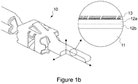
- Figure 1b is a perspective view of a male electrical terminal 10 having a substrate 11, a first metallic conductive layer 12a, a second metallic conductive layer 12b and an organic passivation film 13 according to an embodiment of the present disclosure.
- the organic passivation film 13 comprises an ionic and/or polar organic compound that both protects the underlying silver layer 12 from environmental degradation
- the terminal 10 is optionally a male and/or female connector e.g., push-fit type, that are connectable to provide an electrically conducting junction to establish an electrical conduit or circuit.
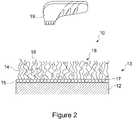
- the organic passivation film 13 comprises a compound having a polar or ionic head group 15 and hydrocarbon tail or chain 14 extending from head group 15.
- Head groups 15 are configured for adsorption at a surface 17 of the electrically conducting layer 12. Depending on the type of head group 15, the adsorption may occur through one or a combination of mechanisms including chemical bonding, crosslinking, electrostatic bonding (ionic or Van der Waals interactions) with the conducting layer 12 at the region of surface 17.
- Passivation film 13 further comprises a fluorophore 16.
- Fluorophore 16 may be retained at the passivation film 13 via any one or a combination of mechanisms including but not limited to entrapment, tethering, entanglement, covalent/chemical bonding and/or electrostatic bonding (ionic or Van der Waals interactions).
- fluorophore 16 is distributed generally homogeneously within passivation film 13 in a plane parallel to surface 17 and/or in a direction perpendicular to surface 17 (in a thickness direction of film 13).
- the fluorophore 16 may be provided at or towards an external surface 18 of film 13 relative to electrically conducting layer 12.
- Terminal 10 having the layered configuration as described, is advantageous, via incorporation of the fluorophore 16, to fluoresce in response to incident electromagnetic radiation.
- a radiation comprises UV light generated/emitted from a UV torch 19 having an internal UV lamp (not shown) powered by a battery or other electrical supply (not shown).
- the present disclosure also relates to an inspection system 20, being apparatus and method to inspect terminals 10 and to determine any one or a combination of characteristics of the terminal including for example the presence of the metallic conductive layer (silver layer 12), a type of metallic conductive layer, the presence or type of the organic passivation film 13, or a thickness or density of the organic passivation film 13.
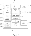
- the system 20 comprises a control unit 32 having a control module 33, a communication module 35 and a processor 34.
- Modules 33 and 35 may be implemented as software present and operational on an electronic machine control unit (MCU) comprising a conventional architecture including a printed circuit board and associated electronic components as described.
- MCU electronic machine control unit
- System 20 further comprises: an image capturing device implemented as a camera 21 having a camera module 22, also implemented as software and hosted at or independently of the control unit 32; and a filter 23 to prevent or minimise capture of electromagnetic radiation emitted directly from an electromagnetic energy source 24. Filter 23 may also be configured to filter ambient electromagnetic radiation to enable camera 21 to capture images resultant substantially or exclusively from the fluorescence emitted from fluorophore 16 within film 13.
- System 20 further comprises an image analysis unit 26 having an analysis module, implemented as software and installed and operational locally at the image analysis unit 26. According to further implementations, analysis module 27 may be hosted and operational at control unit 32.
- Analysis unit 26 via analysis module 27 is configured to analyse images captured by camera 21 and to determine at least one characteristic of the terminal 10 including in particular, a characteristic of passivation film 13 and/or a characteristic of metallic layer 12. Analysis unit 26 may utilise reference library 30 to output a quantitative and/or qualitative output quantifier useful by personnel to identify and/or characterise terminal 10 relative to at least one predefined characteristic (i.e., physical, mechanical, electrical and/or chemical parameters). Control, data input and output at system 20 is managed by a user interacting with the system 20 via a user interface 31 using conventional input means (e.g. a touch screen, keyboard, keypad etc).
- conventional input means e.g. a touch screen, keyboard, keypad etc.
- the power source 29 may comprise a local battery (installed at system 20) or may comprise a socket, terminal or junction to allow coupling of system 20 to a remote power source.
- System 20 may be implemented as a mobile, handheld device or as a desktop device. If implemented as a desktop device, camera 21 and/or image analysis unit 26 may be movably or remotely coupled to system 20 so as to be positionable in close proximity to a terminal 10 to characterise whilst the majority and remaining components of the system 20 may be located remotely.
- system 20 is configured to allow personnel to inspect terminals 10 by emitting electromagnetic energy from UV lamp 25, capturing an image of fluorescence emitted from the fluorophore 16 within layer 13, analysing the image to identify one or more aspects of the terminal 10 and characterise the terminal quantitatively or qualitatively according to predetermined criteria and/or parameters.
- Such terminals 10 may be connected to electrical cables via crimping or ultrasonic welding.
- the electrical cables may be copper or aluminium cables.
- the terminals 10 may be housed in a connector housing and joined to the electrical cables for connection with other related electrical equipment.
- Such a joining structure of the electrical cables and the terminals 10 is achieved by joining the electrical cables to the terminals 10 by various methods such ultrasonic welding.
- a metal passivation layer configured to enable optical/visual identification by fluorescence to confirm the presence and/or material type of the passivation layer on the substrate of the terminals, improved control of an ultrasonic welding process involving the terminals may be achieved.
- organic passivation layer 13 Specific embodiments of the organic passivation layer 13 are described with reference to the following examples.
- a silver-plated substrate was formed by silver plating according to conventional techniques.
- the dual layer structure was immersed in a previously prepared 5 mM solution of SH-(CH 2 ) 17 CH in ethanol for at least 12 hours.
- Fluorescein was added to the solution prior to immersion of the silver-plated substrate at a concentration in the range 1.0 ⁇ 10 -2 mo1/1 to 1.0 ⁇ 10 -7 mol/l (approximately 300 to 700 ppm).
- a chemosorption process occurred to form a continuous uninterrupted passivation layer on the metallic conducting layer.
- the molecules were entrapped within the hydrocarbon tails of the passivation layer via entanglement and Van der Waals interactions.
Landscapes
- Chemical & Material Sciences (AREA)
- Organic Chemistry (AREA)
- Materials Engineering (AREA)
- Engineering & Computer Science (AREA)
- Health & Medical Sciences (AREA)
- Pathology (AREA)
- Physics & Mathematics (AREA)
- General Health & Medical Sciences (AREA)
- General Physics & Mathematics (AREA)
- Immunology (AREA)
- Analytical Chemistry (AREA)
- Life Sciences & Earth Sciences (AREA)
- Biochemistry (AREA)
- Nuclear Medicine, Radiotherapy & Molecular Imaging (AREA)
- Chemical Kinetics & Catalysis (AREA)
- Mechanical Engineering (AREA)
- Metallurgy (AREA)
- Investigating, Analyzing Materials By Fluorescence Or Luminescence (AREA)
- Testing Or Measuring Of Semiconductors Or The Like (AREA)
- Electroluminescent Light Sources (AREA)
- Measuring Leads Or Probes (AREA)
Abstract
Description
- The present invention relates to an electrical contact and in particular, although not exclusively, to an electrically conductive plating on an electrical terminal that is configured to fluoresce as a means of identifying the plating.
- Electrical connectors are typically formed from a base substrate material that is coated with a high conductivity layer to enable contacts to be mated with minimised contact resistance. Example electrical contacts include conductive pins insertable within backplates and male and female push-fit contacts to couple electronic components and/or circuits. Typical electrically conducting plating materials include copper, gold, nickel, silver and alloys thereof.
- Silver as a contact plating provides high conductivity and ductility to allow the connectors to compress together when mated. This maximises the contact area and minimises contact resistance. Silver is also easy to solder. However, silver connectors, unlike other metals such as gold, tends to tarnish in air. Other plating materials may oxidise or can be susceptible to environmental degradation that may affect the conductivity, connection interface or integrity. Accordingly, it is known to apply protective films or layers over the conducting layer to prevent corrosion and/or wear. For example, a lubricating oil may be applied to gold plating for wear resistance. Surfactant based coatings have also been proposed in an attempt to provide protection against corrosive environments and to maintain low contact resistance.
-
US 6,627,329 describes an electrical connector having a plated material protected by a bonding layer of an organic substance and a lubricating layer formed on the bonding layer. The organic substance is capable of combining chemically with the plating layer. - However, it is difficult to differentiate and identify the various types of electrical connectors and contacts in-situ. In particular, it is often problematic for personnel to identify if a contact is coated with, for example, high conductivity silver or is simply a uncoated material such as tin. This can lead to manufactured terminals to be identified incorrectly, which causes connection performance issues when the terminals are installed in the field. Accordingly, what is required is improved electrical connectors and contacts that address these problems.
- It is an objective of the present disclosure to provide an electrical connector having high electrical conductivity, low contact resistance as well as a resistance to environmental effects, wear and tarnishing. It is a further specific objective to provide a coating for an electrical connector that is readily identifiable, preferably optically, to allow optical/visual inspection of a coated substrate to confirm the presence of a type or class of protective passivation layer, such as fundamental material composition. The electrical connector may be a male or female electrical terminal.
- It is a further specific objective to provide a metal passivation layer configured to enable optical/visual identification by fluorescence to confirm the presence and/or material type of the passivation layer on the substrate.
- It is a yet further objective to provide an optical inspection apparatus, system and method enabling the inspection of electrical contacts to confirm the presence and/or a physical, mechanical or chemical characteristic of the passivation layer.
- The objectives are achieved via a coating layer applied to an electrical terminal that incorporates a fluorophore component or compound at a protective passivation film that, in turn, provides a protective characteristic to an underlying metallic conductive layer applied to a substrate.
- The fluorophore may be provided at a polar organic passivation film via any one or a combination of mechanisms including but not limited to entrapment, tethering, entanglement, covalent/chemical bonding, and/or electrostatic bonding such as ionic or Van der Waals interactions.
- According to the present disclosure, the polar organic passivation film may be provided at the substrate via any one or a combination of mechanisms including but not limited to absorption at the metallic conductive layer, chemical bonding with the metallic conductive layer, cross linking with the metallic conductive layer or electrostatic bonding to the metallic conductive layer (ionic or Van der Waals interactions).
- The present disclosure also provides an optical/visual inspection system including apparatus and method for the inspection of electrical terminals to determine any one or a combination of characteristics of the electrical terminals including in particular the presence of a metallic conductive layer, a type of metallic conductive layer, the presence or type of an organic passivation film, and a thickness or density of an organic passivation film.
- According to a first aspect of the present disclosure there is provided a male or female electrical terminal comprising: a substrate; a metallic conductive layer provided on the substrate; an organic passivation film provided on the metallic conductive layer; and a fluorophore provided at the passivation layer.
- Optionally, the organic passivation film comprises a compound having an organic tail and a polar or ionic head group. Optionally, the organic tail comprises a linear, branched, substituted or unsubstituted alkyl or phenyl group. Optionally, the polar or ionic head group comprises any one or a combination of at least one of: a sulphate, a sulfonate, sulphide, a disulphide, an alkyl sulphide, a dialkyl sulphide, a sulfhydryl group, a phosphate, a carboxylate, a carboxyl, a phenolic, an epoxy, an amine, an imine oxide, an ether, an ester, an ethoxylate, a glycerol, a hydroxyl or polyhydroxy.
- Preferably, the compound comprises a C5-C30 saturated or unsaturated alkyl chain and a polar head group comprising a sulfhydryl group. Preferably the compound comprises a thiol. Optionally, the compound comprises C16-C22 saturated linear alkyl chain and a polar head group comprising a sulfhydryl group (i.e., a thiol compound).
- Preferably, the organic passivation film comprises a monomolecular thickness. Optionally, the organic passivation film comprises a bimolecular or multimolecular thickness.
- Optionally, the fluorophore comprises any one or a combination of at least one of: an organic compound; an inorganic compound; a biological fluorophore; a quantum dot.
- Optionally, the fluorophore comprises any one or a combination of at least one of: an anthracene derivative; a quinolone or quinoline derivative; a xanthene or xanthene derivative; a pyrene or pyrene derivative.
- Optionally, the fluorophore comprises any one or a combination of at least one of fluorescein (resorcinolphthalein) or a fluorescein derivative; rhodamine or a rhodamine derivative such as rhodamine 6G (Rh6G), rhodamine 560 (Rh560), sulforhodamine B (SRhB), rhodamine 640 (Rh640), and fluorescein 548 (F1548); or 8-hydroxypyrene-1,3,6-trisulfonic acid trisodium salt.
- Optionally, the metallic conductive layer comprises a metal or metal alloy comprising any one or a combination of at least one of: silver, gold, nickel. Optionally, the substrate comprises any one or a combination of at least one of: copper, a copper alloy, iron, steel, stainless steel.
- According to a further aspect of the present disclosure there is provided an optical inspection system for inspecting electrical terminals comprising: an electromagnetic energy source to emit excitation energy towards an electrical terminal as claimed herein; an image capturing device for capturing an image of the excited electrical terminal; and an optical analysis module for analysing the captured image and determining one or more characteristics of the electrical terminal.
- Optionally, the one or more characteristics of the electrical terminal may include any one or a combination of: the presence or type of the metallic conductive layer, the presence, type, thickness or density of the polar organic passivation film.
- Optionally, the optical inspection system may further comprise any one or a combination of: an electromagnetic energy filter to minimise or eliminate capture of ambient electromagnetic energy and/or electromagnetic energy emitted directly by the electromagnetic energy source; a data storage unit; a user interface; a reference library; a power source; a control unit configured to control any one or a combination of the electromagnetic energy source, the image capturing device, the optical analysis module, the data storage unit, the power source, the user interface or the reference library.
- Optionally, the control unit comprises any one or a combination of a control module, a communication module, and a processor.
- Optionally, the image capturing device comprises a camera to record an image of the electrical terminal. Optionally, the electromagnetic energy source comprises a lamp configured to emit an excitation energy in a range of 100 nm to 750 nm, 100 nm to 60 nm or 100 nm to 400 nm. The wavelength of the electromagnetic energy source may be determined by a spectrometer or spectral radiometer such as a Thermo Scientific™ 201/220 UV visible spectrometer available from Fisher Scientific, UK. Optionally, the electromagnetic energy source comprises a UV lamp. Optionally, the power source further comprises a power source to power the electromagnetic energy source wherein the power source is a battery, a connection socket, a cable and/or a plug for connection to an electricity supply.
- Optionally, the inspection system is configured for the automated or part-automated inspection of electrical terminals. Such automation is implemented via the electronic components, architecture and system function in combination with suitable control software as described. Control, intervention and modification of the operational parameters of the inspection system may be implemented locally or remotely via interrogation of the software via the user interface as described.
- According to a further aspect of the present disclosure there is provided an optical inspection apparatus for inspecting electrical terminals comprising: an electromagnetic energy source to emit excitation energy towards an electrical terminal to enable visual observation of any fluorescence emitted by the electrical terminal.
- A specific implementation of the present disclosure will now be described, by way of example only, and with reference to the accompanying drawings in which:
-
Figure 1a is a cross sectional view through an electrical terminal having a substrate, a metallic conductive layer and an organic passivation film according to a specific implementation; -
Figure 1b is a perspective view of a male electrical terminal having a substrate, a metallic conductive layer and an organic passivation film according to a specific implementation; -
Figure 2 is a magnified cross sectional view of the metallic conductive layer and the passivation film according to the specific implementation; and -
Figure 3 illustrates schematically selected architectural components of an optical inspection system for characterising electrical terminals. - Referring to
figure 1a anelectrical terminal 10, alternatively termed a contact, comprises a primary metallic body forming asubstrate 11.Substrate 11 may be formed from a steel and in particular stainless steel. A silver-plating layer 12 is provided oversubstrate 11.Silver layer 12, relative tosubstrate 11 comprises high electrical conductivity and ductility. A passivation film orlayer 13 is provided over thesilver layer 12.Layer 13 comprises an ionic and/or polar organic compound that both protects theunderlying silver layer 12 from environmental degradation.Layer 13 also comprises a friction coefficient being less than that of asilver layer 12 so as to provide wear protection. Theelectrical terminal 10 may be a male or female electrical terminal. In this regard,Figure 1b is a perspective view of a maleelectrical terminal 10 having asubstrate 11, a first metallicconductive layer 12a, a second metallicconductive layer 12b and anorganic passivation film 13 according to an embodiment of the present disclosure. Theorganic passivation film 13 comprises an ionic and/or polar organic compound that both protects theunderlying silver layer 12 from environmental degradation The terminal 10 is optionally a male and/or female connector e.g., push-fit type, that are connectable to provide an electrically conducting junction to establish an electrical conduit or circuit. - Referring to
figure 2 , theorganic passivation film 13 comprises a compound having a polar orionic head group 15 and hydrocarbon tail orchain 14 extending fromhead group 15.Head groups 15 are configured for adsorption at asurface 17 of theelectrically conducting layer 12. Depending on the type ofhead group 15, the adsorption may occur through one or a combination of mechanisms including chemical bonding, crosslinking, electrostatic bonding (ionic or Van der Waals interactions) with the conductinglayer 12 at the region ofsurface 17.Passivation film 13 further comprises afluorophore 16.Fluorophore 16, according to optional implementations and depending upon the chemical type of thefluorophore 16 andhydrocarbon tail 14, may be retained at thepassivation film 13 via any one or a combination of mechanisms including but not limited to entrapment, tethering, entanglement, covalent/chemical bonding and/or electrostatic bonding (ionic or Van der Waals interactions). Preferably, fluorophore 16 is distributed generally homogeneously withinpassivation film 13 in a plane parallel to surface 17 and/or in a direction perpendicular to surface 17 (in a thickness direction of film 13). Optionally, thefluorophore 16 may be provided at or towards anexternal surface 18 offilm 13 relative to electrically conductinglayer 12. -
Terminal 10, having the layered configuration as described, is advantageous, via incorporation of thefluorophore 16, to fluoresce in response to incident electromagnetic radiation. Such a radiation, according to the preferred embodiment, comprises UV light generated/emitted from aUV torch 19 having an internal UV lamp (not shown) powered by a battery or other electrical supply (not shown). - The present disclosure also relates to an
inspection system 20, being apparatus and method to inspectterminals 10 and to determine any one or a combination of characteristics of the terminal including for example the presence of the metallic conductive layer (silver layer 12), a type of metallic conductive layer, the presence or type of theorganic passivation film 13, or a thickness or density of theorganic passivation film 13. Thesystem 20 comprises acontrol unit 32 having acontrol module 33, acommunication module 35 and aprocessor 34.Modules System 20 further comprises: an image capturing device implemented as acamera 21 having acamera module 22, also implemented as software and hosted at or independently of thecontrol unit 32; and afilter 23 to prevent or minimise capture of electromagnetic radiation emitted directly from anelectromagnetic energy source 24.Filter 23 may also be configured to filter ambient electromagnetic radiation to enablecamera 21 to capture images resultant substantially or exclusively from the fluorescence emitted fromfluorophore 16 withinfilm 13.System 20 further comprises animage analysis unit 26 having an analysis module, implemented as software and installed and operational locally at theimage analysis unit 26. According to further implementations,analysis module 27 may be hosted and operational atcontrol unit 32.Analysis unit 26 viaanalysis module 27 is configured to analyse images captured bycamera 21 and to determine at least one characteristic of the terminal 10 including in particular, a characteristic ofpassivation film 13 and/or a characteristic ofmetallic layer 12.Analysis unit 26 may utilisereference library 30 to output a quantitative and/or qualitative output quantifier useful by personnel to identify and/or characterise terminal 10 relative to at least one predefined characteristic (i.e., physical, mechanical, electrical and/or chemical parameters). Control, data input and output atsystem 20 is managed by a user interacting with thesystem 20 via auser interface 31 using conventional input means (e.g. a touch screen, keyboard, keypad etc). Thepower source 29 may comprise a local battery (installed at system 20) or may comprise a socket, terminal or junction to allow coupling ofsystem 20 to a remote power source.System 20 may be implemented as a mobile, handheld device or as a desktop device. If implemented as a desktop device,camera 21 and/orimage analysis unit 26 may be movably or remotely coupled tosystem 20 so as to be positionable in close proximity to a terminal 10 to characterise whilst the majority and remaining components of thesystem 20 may be located remotely. - In use,
system 20 is configured to allow personnel to inspectterminals 10 by emitting electromagnetic energy fromUV lamp 25, capturing an image of fluorescence emitted from thefluorophore 16 withinlayer 13, analysing the image to identify one or more aspects of the terminal 10 and characterise the terminal quantitatively or qualitatively according to predetermined criteria and/or parameters. -
Such terminals 10 may be connected to electrical cables via crimping or ultrasonic welding. The electrical cables may be copper or aluminium cables. Theterminals 10 may be housed in a connector housing and joined to the electrical cables for connection with other related electrical equipment. Such a joining structure of the electrical cables and theterminals 10 is achieved by joining the electrical cables to theterminals 10 by various methods such ultrasonic welding. By providing a metal passivation layer configured to enable optical/visual identification by fluorescence to confirm the presence and/or material type of the passivation layer on the substrate of the terminals, improved control of an ultrasonic welding process involving the terminals may be achieved. - Specific embodiments of the
organic passivation layer 13 are described with reference to the following examples. - A silver-plated substrate was formed by silver plating according to conventional techniques. The dual layer structure was immersed in a previously prepared 5 mM solution of SH-(CH2)17CH in ethanol for at least 12 hours. Fluorescein was added to the solution prior to immersion of the silver-plated substrate at a concentration in the range 1.0×10⁻² mo1/1 to 1.0×10⁻⁷ mol/l (approximately 300 to 700 ppm). During emersion a chemosorption process occurred to form a continuous uninterrupted passivation layer on the metallic conducting layer. After drying in an air or nitrogen atmosphere, the molecules were entrapped within the hydrocarbon tails of the passivation layer via entanglement and Van der Waals interactions.
- Unless defined otherwise, all technical and scientific terms used herein have the same meaning as commonly understood to one of ordinary skill in the art to which the presently described subject matter pertains.
- Where a range of values is provided, for example, concentration ranges, percentage ranges, or ratio ranges, it is understood that each intervening value, to the tenth of the unit of the lower limit, unless the context clearly dictates otherwise, between the upper and lower limit of that range and any other stated or intervening value in that stated range, is encompassed within the described subject matter. The upper and lower limits of these smaller ranges may independently be included in the smaller ranges, and such embodiments are also encompassed within the described subject matter, subject to any specifically excluded limit in the stated range. Where the stated range includes one or both of the limits, ranges excluding either or both of those included limits are also included in the described subject matter.
- It should be understood that the terms "a" and "an" as used above and elsewhere herein refer to "one or more" of the enumerated components. It will be clear to one of ordinary skill in the art that the use of the singular includes the plural unless specifically stated otherwise. Therefore, the terms "a," "an" and "at least one" are used interchangeably in this application.
- Unless otherwise indicated, all numbers expressing quantities of ingredients, properties such as size, weight, reaction conditions and so forth used in the specification and claims are to the understood as being modified in all instances by the term "about". Accordingly, unless indicated to the contrary, the numerical parameters set forth in the following specification and attached claims are approximations that may vary depending upon the desired properties sought to be obtained by the present subject matter. At the very least, and not as an attempt to limit the application of the doctrine of equivalents to the scope of the claims, each numerical parameter should at least be construed in light of the number of reported significant digits and by applying ordinary rounding techniques.
- Throughout the application, descriptions of various embodiments use "comprising" language; however, it will be understood by one of skill in the art, that in some instances, an embodiment can alternatively be described using the language "consisting essentially of or "consisting of."
Claims (13)
- A male or female electrical terminal comprising:a substrate;a metallic conductive layer provided on the substrate;an organic passivation film provided on the metallic conductive layer; anda fluorophore provided at the passivation layer.
- The terminal as claimed in claim 1, wherein the organic passivation film comprises a compound having an organic tail and a polar or ionic head group.
- The terminal as claimed in claim 2, wherein the organic tail comprises a linear, branched, substituted or unsubstituted alkyl or phenyl group.
- The terminal as claimed in claim 2 or 3, wherein the polar or ionic head group comprises any one or a combination of at least one of: a sulphate, a sulfonate, sulphide, a disulphide, an alkyl sulphide, a dialkyl sulphide, a sulfhydryl group, a phosphate, a carboxylate, a carboxyl, a phenolic, an epoxy, an amine, an imine oxide, an ether, an ester, an ethoxylate, a glycerol, a hydroxyl or polyhydroxy.
- The terminal as claimed in claim 2, wherein the compound comprises a C5-C30 saturated or unsaturated alkyl chain and a polar head group comprising a sulfhydryl group.
- The terminal as claimed in claim 2, wherein the compound comprises C16-C22 saturated linear alkyl chain and a polar head group comprising a sulfhydryl group.
- The terminal as claimed in any preceding claim, wherein the organic passivation film comprises a monomolecular thickness.
- The terminal as claimed in any one of claims 1 to 6, wherein the organic passivation film comprises a bimolecular or multimolecular thickness.
- The terminal as claimed in any preceding claim, wherein the fluorophore comprises any one or a combination of at least one of:• an organic compound• an inorganic compound• a biological fluorophore• a quantum dot.
- The terminal as claimed in any preceding claim, wherein the fluorophore comprises any one or a combination of at least one of:• an anthracene derivative• a quinolone or quinoline derivative• a xanthene or xanthene derivative• a pyrene or pyrene derivative
- The terminal as claimed in any one of claims 1 to 10, wherein the fluorophore comprises any one or a combination of at least one of fluorescein or a fluorescein derivative; rhodamine or a rhodamine derivative such as rhodamine 6G (Rh6G), rhodamine 560 (Rh560), sulforhodamine B (SRhB), rhodamine 640 (Rh640), and fluorescein 548 (F1548); or 8-hydroxypyrene-1,3,6-trisulfonic acid trisodium salt.
- The terminalas claimed in any preceding claim, wherein the metallic conductive layer comprises a metal or metal alloy comprising any one or a combination of at least one of: silver, gold, nickel.
- The terminal as claimed in any preceding claim, wherein the substrate comprises any one or a combination of at least one of: copper, a copper alloy, iron, steel, stainless steel.
Applications Claiming Priority (1)
| Application Number | Priority Date | Filing Date | Title |
|---|---|---|---|
| GB2103380.8A GB2604636A (en) | 2021-03-11 | 2021-03-11 | Electrical Contact with Passivation Layer |
Publications (2)
| Publication Number | Publication Date |
|---|---|
| EP4056666A1 true EP4056666A1 (en) | 2022-09-14 |
| EP4056666B1 EP4056666B1 (en) | 2023-11-01 |
Family
ID=75623054
Family Applications (1)
| Application Number | Title | Priority Date | Filing Date |
|---|---|---|---|
| EP22161023.1A Active EP4056666B1 (en) | 2021-03-11 | 2022-03-09 | Electrical terminal with passivation layer |
Country Status (2)
| Country | Link |
|---|---|
| EP (1) | EP4056666B1 (en) |
| GB (1) | GB2604636A (en) |
Cited By (1)
| Publication number | Priority date | Publication date | Assignee | Title |
|---|---|---|---|---|
| CN118099892A (en) * | 2024-04-24 | 2024-05-28 | 珠海聚能精密工业有限公司 | Corrosion-resistant copper terminal and processing technology thereof |
Citations (2)
| Publication number | Priority date | Publication date | Assignee | Title |
|---|---|---|---|---|
| US6627329B1 (en) | 1998-06-29 | 2003-09-30 | Japan Aviation Electronics Industry | Plated materials and contacts for connectors made by using the same |
| KR20120000974A (en) * | 2010-06-28 | 2012-01-04 | 엘지이노텍 주식회사 | Light emitting device, light emitting device manufacturing method, light emitting device package and lighting system |
-
2021
- 2021-03-11 GB GB2103380.8A patent/GB2604636A/en not_active Withdrawn
-
2022
- 2022-03-09 EP EP22161023.1A patent/EP4056666B1/en active Active
Patent Citations (2)
| Publication number | Priority date | Publication date | Assignee | Title |
|---|---|---|---|---|
| US6627329B1 (en) | 1998-06-29 | 2003-09-30 | Japan Aviation Electronics Industry | Plated materials and contacts for connectors made by using the same |
| KR20120000974A (en) * | 2010-06-28 | 2012-01-04 | 엘지이노텍 주식회사 | Light emitting device, light emitting device manufacturing method, light emitting device package and lighting system |
Non-Patent Citations (1)
| Title |
|---|
| WHITE L. K. ET AL: "The Detection of Corrosion Phenomena with pH-Sensitive Fluorescent Dyes on Aluminum- and Gold-Metallized IC Devices", vol. 128, no. 5, 1 May 1981 (1981-05-01), pages 953 - 956, XP055856830, ISSN: 0013-4651, Retrieved from the Internet <URL:https://citeseerx.ist.psu.edu/viewdoc/download?doi=10.1.1.852.9517&rep=rep1&type=pdf> DOI: 10.1149/1.2127581 * |
Cited By (1)
| Publication number | Priority date | Publication date | Assignee | Title |
|---|---|---|---|---|
| CN118099892A (en) * | 2024-04-24 | 2024-05-28 | 珠海聚能精密工业有限公司 | Corrosion-resistant copper terminal and processing technology thereof |
Also Published As
| Publication number | Publication date |
|---|---|
| EP4056666B1 (en) | 2023-11-01 |
| GB2604636A (en) | 2022-09-14 |
| GB202103380D0 (en) | 2021-04-28 |
Similar Documents
| Publication | Publication Date | Title |
|---|---|---|
| Jellesen et al. | Corrosion failure due to flux residues in an electronic add-on device | |
| US10056707B2 (en) | Electrical contact including corrosion-resistant coating | |
| EP4056666B1 (en) | Electrical terminal with passivation layer | |
| Song | Corrosion behavior and prevention strategies for magnesium (Mg) alloys | |
| Zhan et al. | Reliability of printed circuit boards processed using no-clean flux technology in temperature–humidity–bias conditions | |
| KR101788688B1 (en) | Electronic component | |
| US20120132541A1 (en) | Sub-coating coated metal corrosion measurement | |
| Ambat et al. | Humidity and electronics: corrosion reliability issues and preventive measures | |
| Yadav et al. | Statistical analysis of corrosion failures in hearing aid devices from tropical regions | |
| Antler | Effect of surface contamination on electric contact performance | |
| Antler et al. | Base metal contacts: An exploratory study of separable connection to tin-lead | |
| Dukhi et al. | Formation of corrosive sulfur with dibenzyl disulfide in fluid-filled transformers | |
| Hannigan et al. | Corrosion of RoHS-Compliant surface finishes in corrosive mixed flowing gas environments | |
| Goti | Cost-Benefit Analysis of ENIG vs. HASL vs. OSP for Class 3 PCBs | |
| Li et al. | Alkanolamines as activators in no-clean flux systems: investigation of humidity robustness and solderability | |
| JP2015045045A (en) | METAL MATERIAL FOR ELECTRONIC COMPONENT AND ITS MANUFACTURING METHOD, CONNECTOR TERMINAL USING THE SAME, CONNECTOR AND ELECTRONIC COMPONENT | |
| JP3184375B2 (en) | Method for evaluating and restoring solderability of electronic components | |
| Tegehall | Impact of humidity and contamination on surface insulation resistance and electrochemical migration | |
| Minzari | Investigation of electronic corrosion mechanisms | |
| JP2015045050A (en) | METAL MATERIAL FOR ELECTRONIC COMPONENT AND ITS MANUFACTURING METHOD, CONNECTOR TERMINAL USING THE SAME, CONNECTOR AND ELECTRONIC COMPONENT | |
| JP2015045047A (en) | METAL MATERIAL FOR ELECTRONIC COMPONENT AND ITS MANUFACTURING METHOD, CONNECTOR TERMINAL USING THE SAME, CONNECTOR AND ELECTRONIC COMPONENT | |
| Asikainen et al. | A systematic corrosion failure analysis of Li-ion powered hearing aids from various markets | |
| Bratin et al. | Surface evaluation of the silver finishes via sequential electrochemical reduction analysis (SERA) | |
| Bratin et al. | Evaluating finishes using SERA | |
| Ramírez Rico et al. | Corrosion of old overhead lines: insights into aluminum-steel galvanic couple using electrochemical techniques |
Legal Events
| Date | Code | Title | Description |
|---|---|---|---|
| PUAI | Public reference made under article 153(3) epc to a published international application that has entered the european phase |
Free format text: ORIGINAL CODE: 0009012 |
|
| STAA | Information on the status of an ep patent application or granted ep patent |
Free format text: STATUS: THE APPLICATION HAS BEEN PUBLISHED |
|
| AK | Designated contracting states |
Kind code of ref document: A1 Designated state(s): AL AT BE BG CH CY CZ DE DK EE ES FI FR GB GR HR HU IE IS IT LI LT LU LV MC MK MT NL NO PL PT RO RS SE SI SK SM TR |
|
| STAA | Information on the status of an ep patent application or granted ep patent |
Free format text: STATUS: REQUEST FOR EXAMINATION WAS MADE |
|
| 17P | Request for examination filed |
Effective date: 20230217 |
|
| RAP3 | Party data changed (applicant data changed or rights of an application transferred) |
Owner name: APTIV TECHNOLOGIES LIMITED |
|
| RBV | Designated contracting states (corrected) |
Designated state(s): AL AT BE BG CH CY CZ DE DK EE ES FI FR GB GR HR HU IE IS IT LI LT LU LV MC MK MT NL NO PL PT RO RS SE SI SK SM TR |
|
| GRAP | Despatch of communication of intention to grant a patent |
Free format text: ORIGINAL CODE: EPIDOSNIGR1 |
|
| STAA | Information on the status of an ep patent application or granted ep patent |
Free format text: STATUS: GRANT OF PATENT IS INTENDED |
|
| INTG | Intention to grant announced |
Effective date: 20230531 |
|
| P01 | Opt-out of the competence of the unified patent court (upc) registered |
Effective date: 20230816 |
|
| GRAS | Grant fee paid |
Free format text: ORIGINAL CODE: EPIDOSNIGR3 |
|
| GRAA | (expected) grant |
Free format text: ORIGINAL CODE: 0009210 |
|
| STAA | Information on the status of an ep patent application or granted ep patent |
Free format text: STATUS: THE PATENT HAS BEEN GRANTED |
|
| AK | Designated contracting states |
Kind code of ref document: B1 Designated state(s): AL AT BE BG CH CY CZ DE DK EE ES FI FR GB GR HR HU IE IS IT LI LT LU LV MC MK MT NL NO PL PT RO RS SE SI SK SM TR |
|
| REG | Reference to a national code |
Ref country code: GB Ref legal event code: FG4D |
|
| REG | Reference to a national code |
Ref country code: CH Ref legal event code: EP |
|
| REG | Reference to a national code |
Ref country code: IE Ref legal event code: FG4D |
|
| REG | Reference to a national code |
Ref country code: DE Ref legal event code: R096 Ref document number: 602022000811 Country of ref document: DE |
|
| REG | Reference to a national code |
Ref country code: LT Ref legal event code: MG9D |
|
| REG | Reference to a national code |
Ref country code: NL Ref legal event code: MP Effective date: 20231101 |
|
| PG25 | Lapsed in a contracting state [announced via postgrant information from national office to epo] |
Ref country code: GR Free format text: LAPSE BECAUSE OF FAILURE TO SUBMIT A TRANSLATION OF THE DESCRIPTION OR TO PAY THE FEE WITHIN THE PRESCRIBED TIME-LIMIT Effective date: 20240202 |
|
| PG25 | Lapsed in a contracting state [announced via postgrant information from national office to epo] |
Ref country code: IS Free format text: LAPSE BECAUSE OF FAILURE TO SUBMIT A TRANSLATION OF THE DESCRIPTION OR TO PAY THE FEE WITHIN THE PRESCRIBED TIME-LIMIT Effective date: 20240301 |
|
| PG25 | Lapsed in a contracting state [announced via postgrant information from national office to epo] |
Ref country code: LT Free format text: LAPSE BECAUSE OF FAILURE TO SUBMIT A TRANSLATION OF THE DESCRIPTION OR TO PAY THE FEE WITHIN THE PRESCRIBED TIME-LIMIT Effective date: 20231101 |
|
| REG | Reference to a national code |
Ref country code: AT Ref legal event code: MK05 Ref document number: 1627218 Country of ref document: AT Kind code of ref document: T Effective date: 20231101 |
|
| PG25 | Lapsed in a contracting state [announced via postgrant information from national office to epo] |
Ref country code: NL Free format text: LAPSE BECAUSE OF FAILURE TO SUBMIT A TRANSLATION OF THE DESCRIPTION OR TO PAY THE FEE WITHIN THE PRESCRIBED TIME-LIMIT Effective date: 20231101 |
|
| PG25 | Lapsed in a contracting state [announced via postgrant information from national office to epo] |
Ref country code: AT Free format text: LAPSE BECAUSE OF FAILURE TO SUBMIT A TRANSLATION OF THE DESCRIPTION OR TO PAY THE FEE WITHIN THE PRESCRIBED TIME-LIMIT Effective date: 20231101 |
|
| PG25 | Lapsed in a contracting state [announced via postgrant information from national office to epo] |
Ref country code: ES Free format text: LAPSE BECAUSE OF FAILURE TO SUBMIT A TRANSLATION OF THE DESCRIPTION OR TO PAY THE FEE WITHIN THE PRESCRIBED TIME-LIMIT Effective date: 20231101 |
|
| PG25 | Lapsed in a contracting state [announced via postgrant information from national office to epo] |
Ref country code: NL Free format text: LAPSE BECAUSE OF FAILURE TO SUBMIT A TRANSLATION OF THE DESCRIPTION OR TO PAY THE FEE WITHIN THE PRESCRIBED TIME-LIMIT Effective date: 20231101 Ref country code: LT Free format text: LAPSE BECAUSE OF FAILURE TO SUBMIT A TRANSLATION OF THE DESCRIPTION OR TO PAY THE FEE WITHIN THE PRESCRIBED TIME-LIMIT Effective date: 20231101 Ref country code: IS Free format text: LAPSE BECAUSE OF FAILURE TO SUBMIT A TRANSLATION OF THE DESCRIPTION OR TO PAY THE FEE WITHIN THE PRESCRIBED TIME-LIMIT Effective date: 20240301 Ref country code: GR Free format text: LAPSE BECAUSE OF FAILURE TO SUBMIT A TRANSLATION OF THE DESCRIPTION OR TO PAY THE FEE WITHIN THE PRESCRIBED TIME-LIMIT Effective date: 20240202 Ref country code: ES Free format text: LAPSE BECAUSE OF FAILURE TO SUBMIT A TRANSLATION OF THE DESCRIPTION OR TO PAY THE FEE WITHIN THE PRESCRIBED TIME-LIMIT Effective date: 20231101 Ref country code: BG Free format text: LAPSE BECAUSE OF FAILURE TO SUBMIT A TRANSLATION OF THE DESCRIPTION OR TO PAY THE FEE WITHIN THE PRESCRIBED TIME-LIMIT Effective date: 20240201 Ref country code: AT Free format text: LAPSE BECAUSE OF FAILURE TO SUBMIT A TRANSLATION OF THE DESCRIPTION OR TO PAY THE FEE WITHIN THE PRESCRIBED TIME-LIMIT Effective date: 20231101 Ref country code: PT Free format text: LAPSE BECAUSE OF FAILURE TO SUBMIT A TRANSLATION OF THE DESCRIPTION OR TO PAY THE FEE WITHIN THE PRESCRIBED TIME-LIMIT Effective date: 20240301 |
|
| PG25 | Lapsed in a contracting state [announced via postgrant information from national office to epo] |
Ref country code: SE Free format text: LAPSE BECAUSE OF FAILURE TO SUBMIT A TRANSLATION OF THE DESCRIPTION OR TO PAY THE FEE WITHIN THE PRESCRIBED TIME-LIMIT Effective date: 20231101 Ref country code: RS Free format text: LAPSE BECAUSE OF FAILURE TO SUBMIT A TRANSLATION OF THE DESCRIPTION OR TO PAY THE FEE WITHIN THE PRESCRIBED TIME-LIMIT Effective date: 20231101 Ref country code: PL Free format text: LAPSE BECAUSE OF FAILURE TO SUBMIT A TRANSLATION OF THE DESCRIPTION OR TO PAY THE FEE WITHIN THE PRESCRIBED TIME-LIMIT Effective date: 20231101 Ref country code: NO Free format text: LAPSE BECAUSE OF FAILURE TO SUBMIT A TRANSLATION OF THE DESCRIPTION OR TO PAY THE FEE WITHIN THE PRESCRIBED TIME-LIMIT Effective date: 20240201 Ref country code: LV Free format text: LAPSE BECAUSE OF FAILURE TO SUBMIT A TRANSLATION OF THE DESCRIPTION OR TO PAY THE FEE WITHIN THE PRESCRIBED TIME-LIMIT Effective date: 20231101 Ref country code: HR Free format text: LAPSE BECAUSE OF FAILURE TO SUBMIT A TRANSLATION OF THE DESCRIPTION OR TO PAY THE FEE WITHIN THE PRESCRIBED TIME-LIMIT Effective date: 20231101 |
|
| PG25 | Lapsed in a contracting state [announced via postgrant information from national office to epo] |
Ref country code: DK Free format text: LAPSE BECAUSE OF FAILURE TO SUBMIT A TRANSLATION OF THE DESCRIPTION OR TO PAY THE FEE WITHIN THE PRESCRIBED TIME-LIMIT Effective date: 20231101 |
|
| PG25 | Lapsed in a contracting state [announced via postgrant information from national office to epo] |
Ref country code: CZ Free format text: LAPSE BECAUSE OF FAILURE TO SUBMIT A TRANSLATION OF THE DESCRIPTION OR TO PAY THE FEE WITHIN THE PRESCRIBED TIME-LIMIT Effective date: 20231101 |
|
| PG25 | Lapsed in a contracting state [announced via postgrant information from national office to epo] |
Ref country code: SK Free format text: LAPSE BECAUSE OF FAILURE TO SUBMIT A TRANSLATION OF THE DESCRIPTION OR TO PAY THE FEE WITHIN THE PRESCRIBED TIME-LIMIT Effective date: 20231101 |
|
| PG25 | Lapsed in a contracting state [announced via postgrant information from national office to epo] |
Ref country code: SM Free format text: LAPSE BECAUSE OF FAILURE TO SUBMIT A TRANSLATION OF THE DESCRIPTION OR TO PAY THE FEE WITHIN THE PRESCRIBED TIME-LIMIT Effective date: 20231101 Ref country code: SK Free format text: LAPSE BECAUSE OF FAILURE TO SUBMIT A TRANSLATION OF THE DESCRIPTION OR TO PAY THE FEE WITHIN THE PRESCRIBED TIME-LIMIT Effective date: 20231101 Ref country code: IT Free format text: LAPSE BECAUSE OF FAILURE TO SUBMIT A TRANSLATION OF THE DESCRIPTION OR TO PAY THE FEE WITHIN THE PRESCRIBED TIME-LIMIT Effective date: 20231101 Ref country code: EE Free format text: LAPSE BECAUSE OF FAILURE TO SUBMIT A TRANSLATION OF THE DESCRIPTION OR TO PAY THE FEE WITHIN THE PRESCRIBED TIME-LIMIT Effective date: 20231101 Ref country code: DK Free format text: LAPSE BECAUSE OF FAILURE TO SUBMIT A TRANSLATION OF THE DESCRIPTION OR TO PAY THE FEE WITHIN THE PRESCRIBED TIME-LIMIT Effective date: 20231101 Ref country code: CZ Free format text: LAPSE BECAUSE OF FAILURE TO SUBMIT A TRANSLATION OF THE DESCRIPTION OR TO PAY THE FEE WITHIN THE PRESCRIBED TIME-LIMIT Effective date: 20231101 |
|
| REG | Reference to a national code |
Ref country code: DE Ref legal event code: R097 Ref document number: 602022000811 Country of ref document: DE |
|
| PLBE | No opposition filed within time limit |
Free format text: ORIGINAL CODE: 0009261 |
|
| STAA | Information on the status of an ep patent application or granted ep patent |
Free format text: STATUS: NO OPPOSITION FILED WITHIN TIME LIMIT |
|
| 26N | No opposition filed |
Effective date: 20240802 |
|
| PG25 | Lapsed in a contracting state [announced via postgrant information from national office to epo] |
Ref country code: SI Free format text: LAPSE BECAUSE OF FAILURE TO SUBMIT A TRANSLATION OF THE DESCRIPTION OR TO PAY THE FEE WITHIN THE PRESCRIBED TIME-LIMIT Effective date: 20231101 |
|
| PG25 | Lapsed in a contracting state [announced via postgrant information from national office to epo] |
Ref country code: SI Free format text: LAPSE BECAUSE OF FAILURE TO SUBMIT A TRANSLATION OF THE DESCRIPTION OR TO PAY THE FEE WITHIN THE PRESCRIBED TIME-LIMIT Effective date: 20231101 |
|
| PG25 | Lapsed in a contracting state [announced via postgrant information from national office to epo] |
Ref country code: LU Free format text: LAPSE BECAUSE OF NON-PAYMENT OF DUE FEES Effective date: 20240309 |
|
| PG25 | Lapsed in a contracting state [announced via postgrant information from national office to epo] |
Ref country code: MC Free format text: LAPSE BECAUSE OF FAILURE TO SUBMIT A TRANSLATION OF THE DESCRIPTION OR TO PAY THE FEE WITHIN THE PRESCRIBED TIME-LIMIT Effective date: 20231101 |
|
| PG25 | Lapsed in a contracting state [announced via postgrant information from national office to epo] |
Ref country code: MC Free format text: LAPSE BECAUSE OF FAILURE TO SUBMIT A TRANSLATION OF THE DESCRIPTION OR TO PAY THE FEE WITHIN THE PRESCRIBED TIME-LIMIT Effective date: 20231101 Ref country code: LU Free format text: LAPSE BECAUSE OF NON-PAYMENT OF DUE FEES Effective date: 20240309 |
|
| REG | Reference to a national code |
Ref country code: BE Ref legal event code: MM Effective date: 20240331 |
|
| PG25 | Lapsed in a contracting state [announced via postgrant information from national office to epo] |
Ref country code: BE Free format text: LAPSE BECAUSE OF NON-PAYMENT OF DUE FEES Effective date: 20240331 |
|
| PG25 | Lapsed in a contracting state [announced via postgrant information from national office to epo] |
Ref country code: IE Free format text: LAPSE BECAUSE OF NON-PAYMENT OF DUE FEES Effective date: 20240309 |
|
| PG25 | Lapsed in a contracting state [announced via postgrant information from national office to epo] |
Ref country code: IE Free format text: LAPSE BECAUSE OF NON-PAYMENT OF DUE FEES Effective date: 20240309 Ref country code: BE Free format text: LAPSE BECAUSE OF NON-PAYMENT OF DUE FEES Effective date: 20240331 |
|
| REG | Reference to a national code |
Ref country code: DE Ref legal event code: R081 Ref document number: 602022000811 Country of ref document: DE Owner name: APTIV TECHNOLOGIES AG, CH Free format text: FORMER OWNER: APTIV TECHNOLOGIES LIMITED, ST. MICHAEL, BB |
|
| PG25 | Lapsed in a contracting state [announced via postgrant information from national office to epo] |
Ref country code: RO Free format text: LAPSE BECAUSE OF FAILURE TO SUBMIT A TRANSLATION OF THE DESCRIPTION OR TO PAY THE FEE WITHIN THE PRESCRIBED TIME-LIMIT Effective date: 20231101 |
|
| PG25 | Lapsed in a contracting state [announced via postgrant information from national office to epo] |
Ref country code: CY Free format text: LAPSE BECAUSE OF FAILURE TO SUBMIT A TRANSLATION OF THE DESCRIPTION OR TO PAY THE FEE WITHIN THE PRESCRIBED TIME-LIMIT; INVALID AB INITIO Effective date: 20220309 |
|
| PG25 | Lapsed in a contracting state [announced via postgrant information from national office to epo] |
Ref country code: FI Free format text: LAPSE BECAUSE OF FAILURE TO SUBMIT A TRANSLATION OF THE DESCRIPTION OR TO PAY THE FEE WITHIN THE PRESCRIBED TIME-LIMIT Effective date: 20231101 |
|
| REG | Reference to a national code |
Ref country code: CH Ref legal event code: H13 Free format text: ST27 STATUS EVENT CODE: U-0-0-H10-H13 (AS PROVIDED BY THE NATIONAL OFFICE) Effective date: 20251023 |
|
| PG25 | Lapsed in a contracting state [announced via postgrant information from national office to epo] |
Ref country code: TR Free format text: LAPSE BECAUSE OF FAILURE TO SUBMIT A TRANSLATION OF THE DESCRIPTION OR TO PAY THE FEE WITHIN THE PRESCRIBED TIME-LIMIT Effective date: 20231101 |
|
| PG25 | Lapsed in a contracting state [announced via postgrant information from national office to epo] |
Ref country code: CH Free format text: LAPSE BECAUSE OF NON-PAYMENT OF DUE FEES Effective date: 20250331 |
|
| PGFP | Annual fee paid to national office [announced via postgrant information from national office to epo] |
Ref country code: GB Payment date: 20260204 Year of fee payment: 5 |
|
| PGFP | Annual fee paid to national office [announced via postgrant information from national office to epo] |
Ref country code: DE Payment date: 20260223 Year of fee payment: 5 |
|
| PGFP | Annual fee paid to national office [announced via postgrant information from national office to epo] |
Ref country code: FR Payment date: 20260205 Year of fee payment: 5 |