EP4053994A1 - Microwave system with narrow band coupling and solderless mounting - Google Patents
Microwave system with narrow band coupling and solderless mounting Download PDFInfo
- Publication number
- EP4053994A1 EP4053994A1 EP21159977.4A EP21159977A EP4053994A1 EP 4053994 A1 EP4053994 A1 EP 4053994A1 EP 21159977 A EP21159977 A EP 21159977A EP 4053994 A1 EP4053994 A1 EP 4053994A1
- Authority
- EP
- European Patent Office
- Prior art keywords
- waveguide
- microwave
- microwave system
- waveguide coupler
- cover
- Prior art date
- Legal status (The legal status is an assumption and is not a legal conclusion. Google has not performed a legal analysis and makes no representation as to the accuracy of the status listed.)
- Pending
Links
Images



Classifications
-
- H—ELECTRICITY
- H01—ELECTRIC ELEMENTS
- H01P—WAVEGUIDES; RESONATORS, LINES, OR OTHER DEVICES OF THE WAVEGUIDE TYPE
- H01P5/00—Coupling devices of the waveguide type
- H01P5/08—Coupling devices of the waveguide type for linking dissimilar lines or devices
- H01P5/10—Coupling devices of the waveguide type for linking dissimilar lines or devices for coupling balanced lines or devices with unbalanced lines or devices
- H01P5/107—Hollow-waveguide/strip-line transitions
-
- H—ELECTRICITY
- H01—ELECTRIC ELEMENTS
- H01P—WAVEGUIDES; RESONATORS, LINES, OR OTHER DEVICES OF THE WAVEGUIDE TYPE
- H01P5/00—Coupling devices of the waveguide type
- H01P5/12—Coupling devices having more than two ports
- H01P5/16—Conjugate devices, i.e. devices having at least one port decoupled from one other port
- H01P5/18—Conjugate devices, i.e. devices having at least one port decoupled from one other port consisting of two coupled guides, e.g. directional couplers
- H01P5/181—Conjugate devices, i.e. devices having at least one port decoupled from one other port consisting of two coupled guides, e.g. directional couplers the guides being hollow waveguides
- H01P5/182—Conjugate devices, i.e. devices having at least one port decoupled from one other port consisting of two coupled guides, e.g. directional couplers the guides being hollow waveguides the waveguides being arranged in parallel
Definitions
- the invention generally relates to a microwave system for processing microwave signals.
- microwave modules are connected to the amplifier main body by solder joints between the direct current (DC) and radio frequency (RF) planes.
- DC direct current
- RF radio frequency
- a microwave system configured for processing microwave signals.
- the microwave system comprises at least two microwave modules (MICs), a cover, and a waveguide coupler.
- Each MIC comprises a printed circuit board (PCB) and is coupled to a waveguide-feed of the waveguide coupler.
- the respective PCB is mounted solderless and the cover is mounted solderless, as well.
- the cover is configured to cover the first MIC, the at least second MIC, and at least a portion of the waveguide coupler.
- the elimination of solder joints for mounting the PCBs and the cover significantly simplifies both system assembly and subsequent maintenance and repair work, thus saving costs.
- the solderless mounting of the cover also ensures that the cover can be mounted in a fast manner, thereby reducing the manufacturing costs.
- the cover can be easily removed for maintenance purposes such that a technician, e.g. a service technician, has easy access to the respective components, namely the MICs as well as the waveguide coupler at least partly.
- the integration of at least two MICs allows for larger amplification factors and larger absolute amplitudes of the radio frequency (RF) signals to be achieved. In fact, powers up to 400 W can be realized while simultaneously ensuring easy maintenance of the microwave system due to the direct access provided.
- RF radio frequency
- the cover can also comprise multiple parts which together form the cover as a whole.
- a first part of the cover can be arranged to cover at least the first MIC.
- a second part of the cover can then be arranged to cover the second MIC.
- the parts forming the entire cover are mounted solderless.
- the respective parts are also connected with each other in a detachable manner, e.g. in a solderless manner.
- the cover is also mounted in a non-welded manner.
- the cover is mounted in a detachable manner, thereby enabling access to the components of the microwave system covered by the cover.
- the cover may at least partly be configured as a portion of the waveguide-feed. A major portion (greater than 50 %) of the waveguide-feed or rather the entire waveguide-feed may then be established by the cover and the waveguide coupler. Accordingly, the cover combines the effects of being solderless mounted and advantageously participating in the RF signal feed-in mechanism, thereby providing synergy effects with regard to the manufacturing of the microwave system. Therefore, by removing the cover the components which are involved in the feed-in mechanism are easily accessible.
- the first MIC may be isolated from the at least second MIC by means of the waveguide coupler.
- the waveguide coupler may electrically decouple the MICs from each other.
- the cover may also contribute in decoupling the first MIC and the second MIC from each other. Interference effects based on electrical cross talk between the at least two MICs may thus be reduced. Accordingly, the RF signal quality and/or the coupling characteristics are/is improved.
- the waveguide coupler may have a coupling portion that is associated with a narrow side of the waveguide-feed.
- the individual MICs are coupled with the waveguide coupler via the narrow side of the respective waveguide-feeds.
- Coupling of the individual MICs via the narrow side of the waveguide coupler additionally provides that only a single side of the waveguide coupler has to be machined, e.g. milled, precisely.
- the opposite side of the machined one can be a flat surface, e.g. a surface of an aluminum plate. It is not necessary to precisely machine the respective flat surface.
- the manufacturing costs are significantly reduced, as only one portion of the waveguide coupler has to be manufactured precisely in contrast to the prior art requiring to machine two complex half-shells in a precise manner.
- the coupling portion is associated with the narrow side of the waveguide-feed, a simple and cost-effective design is provided such that the installation space may be compact and the overall dimensions are reduced.
- the waveguide coupler is also less prone to failure since the entire tolerance liability is reduced accordingly.
- the coupling established via the narrow sides enables a simple and compact arrangement of the overall microwave system, particularly the waveguide coupler.
- the waveguide coupler may comprise at least one bottom component comprising at least one recess.
- the waveguide coupler may additionally comprise at least one top component having a flat surface.
- the flat surface of the top component may be correspondingly coupled to the bottom component to close the recess such that waveguide portions are established.
- the bottom component may be a combiner bottom component, splitter bottom component, or the like.
- the top component may be a combiner top component, splitter top component, or the like.
- the top component may be mountable solderless to the bottom component, e.g. via screwing, plugging or sticking. Since the top component comprises only a flat surface, the production thereof may be rather simple.
- the recess may be established by several recess portions each having a rectangular cross section.
- the size of the respective rectangular cross sections differ along the waveguide portions, particularly they are narrowing until the coupling portion and, then, they are widening.
- the relative positions of the recess portions with the rectangular cross section may differ along the waveguide portions such that at least one stepped side of the recess is provided, particularly the side being perpendicular to the plane established by the top component, e.g. the flat surface.
- the waveguide-feed may comprise a cross-sectional rectangular shape having two opposite narrow sides and two opposite broad sides.
- the narrow and broad sides of the waveguide-feed may correspond to the narrow and broad sides of the recess of the bottom component of the waveguide coupler.
- RF radio frequency
- the coupling portion may be located between two waveguide portions integrated within the waveguide coupler.
- the coupling portion may be configured to provide a coupling between the first waveguide portion associated with a first waveguide-feed and a second waveguide portion associated with a second waveguide-feed.
- the coupling portion enables interaction between electromagnetic waves, in particular RF signals, propagating through the first and second waveguide portions.
- signal properties may be varied due to coupling effects.
- the waveguide portions which are arranged on opposite sides of the respective coupling portion, may each terminate at opposite waveguide-feeds.
- the first waveguide portion may terminate at the first waveguide-feed.
- the second waveguide portion may terminate at the second waveguide-feed. Since the waveguide coupler comprises two waveguide-feeds and a coupling portion arranged nearby, a combined signal may be established having improved properties, e.g. an enhanced signal strength (amplitude) in case of being operated as a coupler rather than a splitter/divider.
- the cover may be connectable via a detachable connection, particularly by means of screwing, plugging or sticking.
- the cover may be connectable with regard to the waveguide coupler. Detaching the cover may be achievable without significant effort such that the waveguide coupler, the waveguide-feeds and the coupling portion are easily accessible in case that repair or maintenance work is required. In particular, no microfabrication equipment or measures need to be taken.
- Each of the two waveguide portions may interact with at least one MIC, respectively.
- the waveguide coupler may advantageously decouple the MICs from each other such that direct (non-reflected) interactions between the MICs are impossible.
- the coupling portion of the waveguide coupler interaction between electromagnetic waves propagating through the first and second waveguide portions may interact with each other. Based on the arrangement decoupling is improved, a compact design is achieved, the waveguide is easily accessible (since the components are solderless mounted), and improved signal properties may be achieved.
- the microwave system may comprise at least one radio frequency (RF) port that is established by a coupling structure on the PCB of the respective MIC.
- the RF port enables RF signals to be emitted via the coupling structure into the waveguide-feed coupled to the respective MIC.
- the RF port may also ensure to decouple RF signals from the waveguide-feed. Since the RF port is established by the coupling structure of the respective PCB, the design of the microwave system may be compact.
- the coupling structure is integrated into the PCB of the respective microwave module, namely the MIC.
- the coupling structure relates to the interface between the waveguide, e.g. the hollow conductor with the rectangular cross section, and the PCB of the respective microwave module, namely the MIC.
- the at least one RF port may directly interact with a waveguide portion of the waveguide coupler. Accordingly, no additional intermediate coupling components, such as e.g. antennas, are required.
- the RF signals are directly emitted into the waveguide-feed of the waveguide coupler. Hence, an additional component can be saved, thereby reducing the number of components required for establishing the microwave system.
- This arrangement also allows additional recesses due to separately arranged PCBs to be avoided. Hence, the microwave system is more simple and cost-efficient.
- the microwave system relates to a solid state microwave system due to the PCBs of the microwave modules.
- At least one additional RF component may be arranged at the waveguide coupler.
- the additional RF component may be arranged inside a waveguide portion of the waveguide coupler.
- the additional RF component can be e.g. a filtering element, a sensing element, etc.
- the additional RF component may be an integral part of the waveguide coupler.
- the additional RF component may be milled into the waveguide coupler or a specific mounting structure for mounting the additional RF component may be milled into the waveguide coupler.
- additional RF components can be included in the waveguide coupler, the dimensions of the coupler may still be compact. Since the waveguide coupler is produced via milling anyhow, the integration of the additional RF component as an integral part of the waveguide coupler does not require post-milling production steps. Accordingly, the waveguide coupler is producible at high efficiency although additional RF components may be integrated.
- the at least one additional RF component may be arranged at an input port and/or an output port of the waveguide coupler. Consequently, the coupling portion may remain unmodified such that the coupling mechanism between the electromagnetic waves of the opposite waveguide portions is not influenced. Moreover, the input and output ports of the waveguide coupler may be easily accessible and may be more robust against modification by the integration of an additional RF component, compared to the coupling portion.
- the microwave system may have a power supply line that is at least partially established by means of a flexible material, particularly a polyimide, e.g. Kapton.
- the power supply line may in particular serve power supply for the first and the at least second MIC. Since the power supply line is made from a flexible material, e.g. the polyimide film, arrangement of the power supply line may be more robust with regard to manufacturing tolerances. Further, as the power connection (usually DC but AC is also within the scope of the present disclosure) of the individual MICs is established by means of a flat flexible connector with a Kapton-circuit board, a pure plug-in connection is provided in this regard. Accordingly, repair and maintenance work is significantly simplified.
- the at least two MICs may be electrically connected in parallel with each other.
- they may be connected in parallel with respect to a power supply via the power supply line. Accordingly, they may be independently operated.
- operation of the second MIC could be impossible if a power failure occurs at the first MIC.
- the parallel layout is advantageous.
- One or all of the microwave modules may comprise or consist of a microwave integrated circuit, preferably a monolithic microwave integrated circuit.
- the first and or second MIC may be suitable for emission of RF signals in similar or different RF bands.
- the first and or second MIC may be configured for emission of RF signals within the Ka-band (27 GHz to 31 GHz) and/or the Ku-band (12.75 GHz to 14.50 GHz).
- a waveguide may generally also be called a hollow conductor, hollow wave guide, rectangular wave guide, HF-wave guide, RF-wave guide, hollow-metallic wave guide, etc.
- Waveguide systems may be used in satellite applications which typically have restricted available space for the hollow conductor system.
- the waveguide system is connected to a payload of the satellite, for instance measurement and/or analyzing devices, as well as an antenna system such that the signals can be transmitted between the payload and the antenna system.
- the most demanding requirements are the insertion loss of the hollow conductor system as well as its mass and dimensions since satellite applications generally demand for lightweight and compact systems.
- the microwave system according to the invention provides improved signal properties as the independently emitted RF signals may be coupled with each other, while the overall setup including the waveguide coupler and the cover as well as the MICs is very compact.
- the cover and the PCBs of the MICs are mounted solderless maintenance and repair work may be performed more efficient and at reduced risks of failures.
- the phrase "at least one of A, B, and C", for example, means (A), (B), (C), (A and B), (A and C), (B and C), or (A, B, and C), including all further possible permutations when greater than three elements are listed.
- the term “at least one of A and B” generally means “A and/or B", namely "A” alone, “B” alone or "A and B”.
- Fig. 1 is a schematic drawing of the microwave system 10 (also called system).
- the microwave system 10 comprises a first microwave module (MIC) 12 and a second MIC 14 arranged next to each other.
- MIC microwave module
- the microwave system 10 comprises a cover 16 that is transparently illustrated in Figure 1 .
- the cover 16 is arranged such that it covers at least the first MIC 12 and the second MIC 14.
- the cover 16 may generally comprise multiple parts forming the cover 16 as a whole.
- the cover 16 is mounted by means of screwed connections 18.
- the cover 16 may also be larger in size and may be mounted via additional holes 19.
- the first MIC 12 comprises a printed circuit board (PCB) 20.
- the second MIC 14 comprises a second PCB 22.
- both MICs 12, 14 could also include only a single PCB, namely a common PCB.
- the microwave system 10 is directly or indirectly mounted to a single system-PCB 23. Accordingly, the additional screw holes 19 may not only be used for mounting the cover 16 but also for mounting the system-PCB 23.
- the first MIC 12 is coupled to an external power supply line by means of a first flexible detachable connector 24.
- the connector 24 may be configured for plug-in connections.
- the second MIC 14 is coupled to an external power supply line by means of a second flexible detachable connector 26.
- the microwave system 10 comprises a first radio frequency (RF) port 28 and a second RF port 30.
- the first RF port 28 is arranged at a first waveguide-feed 32.
- the second RF port 30 is arranged at a second waveguide-feed 34.
- the RF ports 28, 30 may represent splitter/combiner interaction ports, which may depend on the respective operation mode of the microwave system 10.
- the RF ports 28, 30 may comprise printed waveguide-to-coaxial adaptors or these may be associated thereto. Accordingly, an electromagnetic wave (in particular an RF signal) may be collected by the second RF port 30 at the corresponding waveguide-feed 34, fed by means of portions/arms of a coaxial supply line 36 to the first MIC 12 and/or the second MIC 14.
- the RF signals may be amplified. Subsequently, the signals are transmitted using the coaxial supply line 36 to the first RF port 28. Finally, RF electromagnetic waves may be emitted into the corresponding waveguide-feed 32 despite having increased amplitudes or, generally, modified wave properties.
- Fig. 2 is a cross-sectional view of the microwave system 10 including the waveguide coupler 38 and the cover 16 according to the intersection line A-A indicated in Fig. 1 .
- Fig. 2 some additional components are shown in this cross-sectional view.
- the cover 16 covers the first MIC 12 (and the second MIC 14 which is not shown as to the cross-sectional view).
- the first waveguide-feed 32 and the second waveguide-feed 34 there are the first waveguide-feed 32 and the second waveguide-feed 34.
- the cover 16 is configured such that it partially forms the first and second waveguide-feeds 32, 34.
- the waveguide coupler 38 comprises a bottom component 40, a first top component 42, and a second top component 44.
- the first top component 42 may be considered a combiner top.
- the second top component 44 may be considered a splitter top.
- the top components 42, 44 may also be established in an integrated manner, thereby establishing a single top component.
- the bottom component 40 and the top components 42, 44 substantially form the waveguide coupler 38 as a whole.
- the components 40, 42, 44 of the waveguide coupler 38 comprise corresponding recesses such that together with the system PCB 23 and the cover 16 they establish the waveguide-feeds 32, 34.
- the system PCB 23 and the cover 16 are mounted solderless, thereby providing the above-mentioned advantages with regard to repair and maintenance work.
- Fig. 3 is a schematic drawing of the power supply line 48. Some of the before mentioned components are omitted for improved visibility.
- the power supply line 48 is configured to provide DC power for the first and second MICs 12, 14 via the plug-in connectors 24, 26. Since the power supply line 48 is configured as a plug-in connection without solder joints, the electrical connection can be detached without any problems.
- Fig. 4 is a schematic drawing of the waveguide coupler 38.
- the waveguide coupler 38 comprises a bottom component 40 and top components, only one of which is shown here, i.e. the first top component 42.
- the waveguide coupler 38 as a whole may also comprise only a single top component as already indicated above.
- the waveguide coupler 38 comprises several inputs and/or outputs 52a, 52b, 52c. Moreover, at the inputs/outputs 52a, 52b, 52c additional connection members (may also be referred to as connection flanges) are attached 54a, 54b, 54c, 54d. Likewise, at these positions additional waveguide components, such as filters, could be applied as well. However, these are optional components serving for establishing a connection between the waveguide coupler 38 and external hollow conductor components, e.g. for improving the coupling characteristics.
- the top component 42 is mounted by means of screwed connections 56 to the bottom component 40. Only a single screw is shown, but generally there may be a plurality of screws.
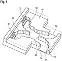
- Fig. 5 is a schematic drawing of the bottom component 40 of the waveguide coupler 38.
- the top component 42 is omitted for visibility reasons.
- the bottom component 40 comprises a first waveguide portion 58 and a second waveguide portion 60.
- the first waveguide portion 58 comprises or is associated to a first waveguide-feed 32 and a first waveguide output 62.
- the second waveguide portion 60 comprises or is associated to a second waveguide-feed 64 and a second waveguide output 66.
- the first waveguide-feed 32 and the second waveguide-feed 64 shown in Fig. 5 are arranged on the same side relative to the system-PCB 23. Accordingly, they generally represent both either splitter interaction ports or combiner interaction ports.
- the waveguide coupler 38 comprises a coupling portion 68 arranged at the bottom component 40 which generally allows for an interaction to take place between the first waveguide portion 58 and the second waveguide portion 60 with regard to the propagation of electromagnetic waves.
- the coupling portion 68 is arranged such that the first waveguide-feed 32 and the second waveguide-feed 64 are decoupled by the waveguide coupler 38.
- the waveguide coupler 38 in particular the bottom component 40, comprises a wall structure such that no electromagnetic waves can directly propagate from the first waveguide-feed 32 to the second waveguide-feed 64 or vice versa. This is achieved by arranging the coupling portion 68 at a lateral distance of the waveguide-feeds 32, 64.
- the hollow portion of the waveguide coupler 38 has a rectangular cross-sectional shape with parallel opposite narrow sides 70 and parallel opposite broad sides 72.
- the rectangular shape may basically be established entirely with regard to the bottom component 40 of the waveguide coupler 38. This shape allows for total reflection conditions such that the electromagnetic waves may propagate without significant losses.
- the coupling portion 68 is associated with the narrow side 70 of the hollow portion of the waveguide coupler 38. Since the coupling portion 68 is associated with the narrow side 70 of the waveguide coupler 38, the top component 42 of the waveguide coupler 38 may comprise a flat surface, e.g. a non-machined one.
- the hollow portion of the waveguide coupler 38 is then completed if the top component 42 is fixed to the bottom component 40, thereby closing or rather covering the recess.
- no cutouts/recesses with a shape corresponding to the hollow portions of the bottom component 40 have to be produced/milled inside the top component 42. Accordingly, the production of the top component 42 of the waveguide coupler 38 is very simple.
- the bottom component 40 and the top component 42 can be stacked on each other very easily without taking any relative positions into account, which would be necessary in case of using complex parts for both sides.
- the waveguide coupler 38 can be produced via milling.
- the waveguide coupler 38 can comprise or be made of aluminum (Al) or similar appropriate lightweight materials.
- Fig. 6 is a schematic drawing of a waveguide-feed 32 according to the present disclosure.
- the waveguide-feed 32 is associated with the first waveguide portion 58 of the bottom component 40 of the waveguide coupler 38.
- a RF port 28 is arranged at the waveguide-feed 32.
- the RF port 28 is generally configured to emit electromagnetic waves, in particular RF signals via the coupling structure 74.
- the coupling structure 74 is associated to the RF port 28 at the waveguide-feed 32.
- the second waveguide-feed 64 comprises similar components, although not shown here.
- the RF port 28 and its corresponding coupling structure 74 is associated with the printed circuit board of the respective MIC. Accordingly, the coupling structure 74 is integrated into the respective PCB of the respective microwave module, namely the MIC. In fact, the coupling structure 74 relates to the interface between the waveguide portion 58, e.g. the hollow conductor with the rectangular cross section, and the PCB of the respective microwave module, namely the MIC.
- the present application may reference quantities and numbers. Unless specifically stated, such quantities and numbers are not to be considered restrictive, but exemplary of the possible quantities or numbers associated with the present application. Also in this regard, the present application may use the term “plurality” to reference a quantity or number. In this regard, the term “plurality” is meant to be any number that is more than one, for example, two, three, four, five, etc. The terms “about”, “approximately”, “near” etc., mean plus or minus 5% of the stated value.
Landscapes
- Waveguide Connection Structure (AREA)
Abstract
Description
- The invention generally relates to a microwave system for processing microwave signals.
- In known microwave applications, such as solid-state microwave amplifiers (e.g. satcom or broadband amplifiers), coupling is usually performed at the so-called broad side of the rectangular coupler, also called waveguide coupler. This coupling arrangement results in an acceptable coupling with regard to the restricted space requirements. However, this arrangement also comprises some disadvantages. Firstly, the coupler has to be split in the middle, resulting in two half shells that together establish the coupler. This means that two complex half-shells have to be manufactured in order to ensure the desired coupling characteristics, whose precision requirements are thus extremely high. Secondly, the microwave modules are connected to the amplifier main body by solder joints between the direct current (DC) and radio frequency (RF) planes. In particular, the RF connections are critical and prone to tolerances. The RF connections are commonly one of the most difficult parts to manufacture and align, such as in case of broadband amplifiers. As a consequence, repair and maintenance can only be conducted by specialized experts at the factory site and even then involves a severe risk of damage.
- Moreover, in known microwave amplifiers, separate antenna elements are commonly used for feeding (coupling-in) the RF signals into the waveguide. As the printed circuit boards of the microwave modules show some variations with regard to each other due to production tolerances (due to fraying and displacement of the metallization), the feeding mechanism of the RF signals suffers thereof.
- Accordingly, there exists a need for a microwave system, which is more robust against production tolerances, which is compact and lightweight, which allows for cost-effective maintenance and repair work, and which provides an improved RF feeding mechanism.
- The subject matter of the independent claim satisfies the respective need. Preferred embodiments are indicated within the dependent claims and the following description, each of which, individually or in combination, may represent aspects of the present disclosure.
- A summary of certain embodiments disclosed herein is set forth below. It should be understood that these aspects are presented merely to provide a brief summary of these certain embodiments and that these aspects are not intended to limit the scope of this disclosure. This disclosure may encompass a variety of aspects that may not be set forth below.
- According to a first aspect, a microwave system is provided. The microwave system is configured for processing microwave signals. The microwave system comprises at least two microwave modules (MICs), a cover, and a waveguide coupler. Each MIC comprises a printed circuit board (PCB) and is coupled to a waveguide-feed of the waveguide coupler. The respective PCB is mounted solderless and the cover is mounted solderless, as well. The cover is configured to cover the first MIC, the at least second MIC, and at least a portion of the waveguide coupler.
- The elimination of solder joints for mounting the PCBs and the cover significantly simplifies both system assembly and subsequent maintenance and repair work, thus saving costs. In addition, the solderless mounting of the cover also ensures that the cover can be mounted in a fast manner, thereby reducing the manufacturing costs. In fact, the cover can be easily removed for maintenance purposes such that a technician, e.g. a service technician, has easy access to the respective components, namely the MICs as well as the waveguide coupler at least partly. Furthermore, the integration of at least two MICs allows for larger amplification factors and larger absolute amplitudes of the radio frequency (RF) signals to be achieved. In fact, powers up to 400 W can be realized while simultaneously ensuring easy maintenance of the microwave system due to the direct access provided.
- In an alternative, the cover can also comprise multiple parts which together form the cover as a whole. In this case, a first part of the cover can be arranged to cover at least the first MIC. A second part of the cover can then be arranged to cover the second MIC. However, the parts forming the entire cover are mounted solderless. In addition, the respective parts are also connected with each other in a detachable manner, e.g. in a solderless manner.
- Generally, the cover, particularly its parts, is also mounted in a non-welded manner. Put differently, the cover is mounted in a detachable manner, thereby enabling access to the components of the microwave system covered by the cover.
- The cover may at least partly be configured as a portion of the waveguide-feed. A major portion (greater than 50 %) of the waveguide-feed or rather the entire waveguide-feed may then be established by the cover and the waveguide coupler. Accordingly, the cover combines the effects of being solderless mounted and advantageously participating in the RF signal feed-in mechanism, thereby providing synergy effects with regard to the manufacturing of the microwave system. Therefore, by removing the cover the components which are involved in the feed-in mechanism are easily accessible.
- The first MIC may be isolated from the at least second MIC by means of the waveguide coupler. In particular, the waveguide coupler may electrically decouple the MICs from each other. Moreover, the cover may also contribute in decoupling the first MIC and the second MIC from each other. Interference effects based on electrical cross talk between the at least two MICs may thus be reduced. Accordingly, the RF signal quality and/or the coupling characteristics are/is improved.
- The waveguide coupler may have a coupling portion that is associated with a narrow side of the waveguide-feed. Hence, the individual MICs are coupled with the waveguide coupler via the narrow side of the respective waveguide-feeds. Coupling of the individual MICs via the narrow side of the waveguide coupler additionally provides that only a single side of the waveguide coupler has to be machined, e.g. milled, precisely. In contrast, the opposite side of the machined one can be a flat surface, e.g. a surface of an aluminum plate. It is not necessary to precisely machine the respective flat surface. Hence, the manufacturing costs are significantly reduced, as only one portion of the waveguide coupler has to be manufactured precisely in contrast to the prior art requiring to machine two complex half-shells in a precise manner. Since the coupling portion is associated with the narrow side of the waveguide-feed, a simple and cost-effective design is provided such that the installation space may be compact and the overall dimensions are reduced. The waveguide coupler is also less prone to failure since the entire tolerance liability is reduced accordingly. Generally, the coupling established via the narrow sides enables a simple and compact arrangement of the overall microwave system, particularly the waveguide coupler.
- The waveguide coupler may comprise at least one bottom component comprising at least one recess. The waveguide coupler may additionally comprise at least one top component having a flat surface. The flat surface of the top component may be correspondingly coupled to the bottom component to close the recess such that waveguide portions are established. The bottom component may be a combiner bottom component, splitter bottom component, or the like. The top component may be a combiner top component, splitter top component, or the like. The top component may be mountable solderless to the bottom component, e.g. via screwing, plugging or sticking. Since the top component comprises only a flat surface, the production thereof may be rather simple.
- In general, the recess may be established by several recess portions each having a rectangular cross section. The size of the respective rectangular cross sections differ along the waveguide portions, particularly they are narrowing until the coupling portion and, then, they are widening. However, the relative positions of the recess portions with the rectangular cross section may differ along the waveguide portions such that at least one stepped side of the recess is provided, particularly the side being perpendicular to the plane established by the top component, e.g. the flat surface.
- The waveguide-feed may comprise a cross-sectional rectangular shape having two opposite narrow sides and two opposite broad sides. The narrow and broad sides of the waveguide-feed may correspond to the narrow and broad sides of the recess of the bottom component of the waveguide coupler. For the propagation of radio frequency (RF) signals rectangular shapes allow standing waves to be achieved (total reflection). Thus, the dissipation of the electromagnetic signals may be reduced.
- The coupling portion may be located between two waveguide portions integrated within the waveguide coupler. The coupling portion may be configured to provide a coupling between the first waveguide portion associated with a first waveguide-feed and a second waveguide portion associated with a second waveguide-feed. Thus, the coupling portion enables interaction between electromagnetic waves, in particular RF signals, propagating through the first and second waveguide portions. As a result, signal properties may be varied due to coupling effects.
- The waveguide portions, which are arranged on opposite sides of the respective coupling portion, may each terminate at opposite waveguide-feeds. In particular, the first waveguide portion may terminate at the first waveguide-feed. The second waveguide portion may terminate at the second waveguide-feed. Since the waveguide coupler comprises two waveguide-feeds and a coupling portion arranged nearby, a combined signal may be established having improved properties, e.g. an enhanced signal strength (amplitude) in case of being operated as a coupler rather than a splitter/divider.
- The cover may be connectable via a detachable connection, particularly by means of screwing, plugging or sticking. Preferably, the cover may be connectable with regard to the waveguide coupler. Detaching the cover may be achievable without significant effort such that the waveguide coupler, the waveguide-feeds and the coupling portion are easily accessible in case that repair or maintenance work is required. In particular, no microfabrication equipment or measures need to be taken.
- Each of the two waveguide portions may interact with at least one MIC, respectively. As the coupling portion is located in between those portions, the waveguide coupler may advantageously decouple the MICs from each other such that direct (non-reflected) interactions between the MICs are impossible. Moreover, by means of the coupling portion of the waveguide coupler interaction between electromagnetic waves propagating through the first and second waveguide portions may interact with each other. Based on the arrangement decoupling is improved, a compact design is achieved, the waveguide is easily accessible (since the components are solderless mounted), and improved signal properties may be achieved.
- The microwave system may comprise at least one radio frequency (RF) port that is established by a coupling structure on the PCB of the respective MIC. The RF port enables RF signals to be emitted via the coupling structure into the waveguide-feed coupled to the respective MIC. Moreover, the RF port may also ensure to decouple RF signals from the waveguide-feed. Since the RF port is established by the coupling structure of the respective PCB, the design of the microwave system may be compact.
- In other words, the coupling structure is integrated into the PCB of the respective microwave module, namely the MIC. In fact, the coupling structure relates to the interface between the waveguide, e.g. the hollow conductor with the rectangular cross section, and the PCB of the respective microwave module, namely the MIC.
- Thus, the at least one RF port may directly interact with a waveguide portion of the waveguide coupler. Accordingly, no additional intermediate coupling components, such as e.g. antennas, are required. The RF signals are directly emitted into the waveguide-feed of the waveguide coupler. Hence, an additional component can be saved, thereby reducing the number of components required for establishing the microwave system. This arrangement also allows additional recesses due to separately arranged PCBs to be avoided. Hence, the microwave system is more simple and cost-efficient.
- Generally, the microwave system relates to a solid state microwave system due to the PCBs of the microwave modules.
- At least one additional RF component may be arranged at the waveguide coupler. In particular, the additional RF component may be arranged inside a waveguide portion of the waveguide coupler. The additional RF component can be e.g. a filtering element, a sensing element, etc.
- In an alternative, the additional RF component may be an integral part of the waveguide coupler. In particular, the additional RF component may be milled into the waveguide coupler or a specific mounting structure for mounting the additional RF component may be milled into the waveguide coupler. Although additional RF components can be included in the waveguide coupler, the dimensions of the coupler may still be compact. Since the waveguide coupler is produced via milling anyhow, the integration of the additional RF component as an integral part of the waveguide coupler does not require post-milling production steps. Accordingly, the waveguide coupler is producible at high efficiency although additional RF components may be integrated.
- In particular, the at least one additional RF component may be arranged at an input port and/or an output port of the waveguide coupler. Consequently, the coupling portion may remain unmodified such that the coupling mechanism between the electromagnetic waves of the opposite waveguide portions is not influenced. Moreover, the input and output ports of the waveguide coupler may be easily accessible and may be more robust against modification by the integration of an additional RF component, compared to the coupling portion.
- The microwave system may have a power supply line that is at least partially established by means of a flexible material, particularly a polyimide, e.g. Kapton. The power supply line may in particular serve power supply for the first and the at least second MIC. Since the power supply line is made from a flexible material, e.g. the polyimide film, arrangement of the power supply line may be more robust with regard to manufacturing tolerances. Further, as the power connection (usually DC but AC is also within the scope of the present disclosure) of the individual MICs is established by means of a flat flexible connector with a Kapton-circuit board, a pure plug-in connection is provided in this regard. Accordingly, repair and maintenance work is significantly simplified.
- The at least two MICs may be electrically connected in parallel with each other. In particular, they may be connected in parallel with respect to a power supply via the power supply line. Accordingly, they may be independently operated. In case of a serial electrical connection, operation of the second MIC could be impossible if a power failure occurs at the first MIC. Hence, the parallel layout is advantageous.
- One or all of the microwave modules may comprise or consist of a microwave integrated circuit, preferably a monolithic microwave integrated circuit.
- The first and or second MIC may be suitable for emission of RF signals in similar or different RF bands. In particular, the first and or second MIC may be configured for emission of RF signals within the Ka-band (27 GHz to 31 GHz) and/or the Ku-band (12.75 GHz to 14.50 GHz).
- A waveguide may generally also be called a hollow conductor, hollow wave guide, rectangular wave guide, HF-wave guide, RF-wave guide, hollow-metallic wave guide, etc.
- Waveguide systems may be used in satellite applications which typically have restricted available space for the hollow conductor system. The waveguide system is connected to a payload of the satellite, for instance measurement and/or analyzing devices, as well as an antenna system such that the signals can be transmitted between the payload and the antenna system. In satellite applications, the most demanding requirements are the insertion loss of the hollow conductor system as well as its mass and dimensions since satellite applications generally demand for lightweight and compact systems. The microwave system according to the invention provides improved signal properties as the independently emitted RF signals may be coupled with each other, while the overall setup including the waveguide coupler and the cover as well as the MICs is very compact. Moreover, as the cover and the PCBs of the MICs are mounted solderless maintenance and repair work may be performed more efficient and at reduced risks of failures.
- The forgoing aspects and further advantages of the claimed subject matter will become more readily appreciated as the same become better understood by reference to the following detailed description when taken in conjunction with the accompanying drawings. In the drawings,
-
Fig. 1 is a schematic drawing of the microwave system according to the invention; -
Fig. 2 is a cross-sectional view of the microwave system including the waveguide coupler and the cover according to the intersection line indicated inFig. 1 ; -
Fig. 3 is a schematic drawing of the power supply line used by the microwave system according to the invention; -
Fig. 4 is a schematic drawing of the waveguide coupler used by the microwave system according to the invention; -
Fig. 5 is a schematic drawing of the bottom component of the waveguide coupler used by the microwave system according to the invention; and -
Fig. 6 is a schematic drawing of a waveguide-feed used by the microwave system according to the invention. - The detailed description set forth below in connection with the appended drawings, where like numerals reference like elements, is intended as a description of various embodiments of the disclosed subject matter and is not intended to represent the only embodiments. Each embodiment described in this disclosure is provided merely as an example or illustration and should not be construed as preferred or advantageous over other embodiments. The illustrative examples provided herein are not intended to be exhaustive or to limit the claimed subject matter to the precise forms disclosed. Various modifications to the described embodiments will be readily apparent to those skilled in the art, and the general principles defined herein may be applied to other embodiments and applications without departing from the spirit and scope of the described embodiments. Thus, the described embodiments are not limited to the embodiments shown, but are to be accorded the widest scope consistent with the principles and features disclosed herein.
- All of the features disclosed hereinafter with respect to the example embodiments and/or the accompanying figures can alone or in any subcombination be combined with features of the aspects of the present disclosure including features of preferred embodiments thereof, provided the resulting feature combination is reasonable to a person skilled in the art.
- For the purposes of the present disclosure, the phrase "at least one of A, B, and C", for example, means (A), (B), (C), (A and B), (A and C), (B and C), or (A, B, and C), including all further possible permutations when greater than three elements are listed. In other words, the term "at least one of A and B" generally means "A and/or B", namely "A" alone, "B" alone or "A and B".
-
Fig. 1 is a schematic drawing of the microwave system 10 (also called system). Themicrowave system 10 comprises a first microwave module (MIC) 12 and asecond MIC 14 arranged next to each other. - The
microwave system 10 comprises acover 16 that is transparently illustrated inFigure 1 . Thecover 16 is arranged such that it covers at least thefirst MIC 12 and thesecond MIC 14. Thecover 16 may generally comprise multiple parts forming thecover 16 as a whole. Thecover 16 is mounted by means of screwedconnections 18. Thecover 16 may also be larger in size and may be mounted viaadditional holes 19. - The
first MIC 12 comprises a printed circuit board (PCB) 20. Thesecond MIC 14 comprises asecond PCB 22. Generally, bothMICs - As shown in
Figure 1 , themicrowave system 10 is directly or indirectly mounted to a single system-PCB 23. Accordingly, the additional screw holes 19 may not only be used for mounting thecover 16 but also for mounting the system-PCB 23. - The
first MIC 12 is coupled to an external power supply line by means of a first flexibledetachable connector 24. Theconnector 24 may be configured for plug-in connections. Similar, thesecond MIC 14 is coupled to an external power supply line by means of a second flexibledetachable connector 26. - The
microwave system 10 comprises a first radio frequency (RF)port 28 and asecond RF port 30. Thefirst RF port 28 is arranged at a first waveguide-feed 32. Thesecond RF port 30 is arranged at a second waveguide-feed 34. TheRF ports microwave system 10. TheRF ports second RF port 30 at the corresponding waveguide-feed 34, fed by means of portions/arms of acoaxial supply line 36 to thefirst MIC 12 and/or thesecond MIC 14. There, the RF signals may be amplified. Subsequently, the signals are transmitted using thecoaxial supply line 36 to thefirst RF port 28. Finally, RF electromagnetic waves may be emitted into the corresponding waveguide-feed 32 despite having increased amplitudes or, generally, modified wave properties. -
Fig. 2 is a cross-sectional view of themicrowave system 10 including thewaveguide coupler 38 and thecover 16 according to the intersection line A-A indicated inFig. 1 . Thus, compared toFig. 1 some additional components are shown in this cross-sectional view. - There is the
first MIC 12 and thesystem PCB 23. Thecover 16 covers the first MIC 12 (and thesecond MIC 14 which is not shown as to the cross-sectional view). In addition, there are the first waveguide-feed 32 and the second waveguide-feed 34. Thecover 16 is configured such that it partially forms the first and second waveguide-feeds - The
waveguide coupler 38 comprises abottom component 40, a firsttop component 42, and a secondtop component 44. The firsttop component 42 may be considered a combiner top. The secondtop component 44 may be considered a splitter top. However, thetop components - The
bottom component 40 and thetop components waveguide coupler 38 as a whole. Thecomponents waveguide coupler 38 comprise corresponding recesses such that together with thesystem PCB 23 and thecover 16 they establish the waveguide-feeds system PCB 23 and thecover 16 are mounted solderless, thereby providing the above-mentioned advantages with regard to repair and maintenance work. - There is shown as well the
external bias board 50 which provides a flexible electricalpower supply line 48 for the first andsecond MICs -
Fig. 3 is a schematic drawing of thepower supply line 48. Some of the before mentioned components are omitted for improved visibility. Thepower supply line 48 is configured to provide DC power for the first andsecond MICs connectors power supply line 48 is configured as a plug-in connection without solder joints, the electrical connection can be detached without any problems. -
Fig. 4 is a schematic drawing of thewaveguide coupler 38. Thewaveguide coupler 38 comprises abottom component 40 and top components, only one of which is shown here, i.e. the firsttop component 42. Generally, thewaveguide coupler 38 as a whole may also comprise only a single top component as already indicated above. - The
waveguide coupler 38 comprises several inputs and/oroutputs outputs waveguide coupler 38 and external hollow conductor components, e.g. for improving the coupling characteristics. Thetop component 42 is mounted by means of screwedconnections 56 to thebottom component 40. Only a single screw is shown, but generally there may be a plurality of screws. -
Fig. 5 is a schematic drawing of thebottom component 40 of thewaveguide coupler 38. Thetop component 42 is omitted for visibility reasons. Thebottom component 40 comprises afirst waveguide portion 58 and asecond waveguide portion 60. Thefirst waveguide portion 58 comprises or is associated to a first waveguide-feed 32 and afirst waveguide output 62. Thesecond waveguide portion 60 comprises or is associated to a second waveguide-feed 64 and asecond waveguide output 66. Notably, the first waveguide-feed 32 and the second waveguide-feed 64 shown inFig. 5 are arranged on the same side relative to the system-PCB 23. Accordingly, they generally represent both either splitter interaction ports or combiner interaction ports. - The
waveguide coupler 38 comprises acoupling portion 68 arranged at thebottom component 40 which generally allows for an interaction to take place between thefirst waveguide portion 58 and thesecond waveguide portion 60 with regard to the propagation of electromagnetic waves. - As can be seen from the figure, the
coupling portion 68 is arranged such that the first waveguide-feed 32 and the second waveguide-feed 64 are decoupled by thewaveguide coupler 38. In other words, thewaveguide coupler 38, in particular thebottom component 40, comprises a wall structure such that no electromagnetic waves can directly propagate from the first waveguide-feed 32 to the second waveguide-feed 64 or vice versa. This is achieved by arranging thecoupling portion 68 at a lateral distance of the waveguide-feeds - The hollow portion of the
waveguide coupler 38 has a rectangular cross-sectional shape with parallel oppositenarrow sides 70 and parallel oppositebroad sides 72. - The rectangular shape may basically be established entirely with regard to the
bottom component 40 of thewaveguide coupler 38. This shape allows for total reflection conditions such that the electromagnetic waves may propagate without significant losses. - Notably, the
coupling portion 68 is associated with thenarrow side 70 of the hollow portion of thewaveguide coupler 38. Since thecoupling portion 68 is associated with thenarrow side 70 of thewaveguide coupler 38, thetop component 42 of thewaveguide coupler 38 may comprise a flat surface, e.g. a non-machined one. - The hollow portion of the
waveguide coupler 38 is then completed if thetop component 42 is fixed to thebottom component 40, thereby closing or rather covering the recess. In particular, no cutouts/recesses with a shape corresponding to the hollow portions of thebottom component 40 have to be produced/milled inside thetop component 42. Accordingly, the production of thetop component 42 of thewaveguide coupler 38 is very simple. In addition, thebottom component 40 and thetop component 42 can be stacked on each other very easily without taking any relative positions into account, which would be necessary in case of using complex parts for both sides. - In the prior art, coupling between waveguide portions via the broad side was done. However, this results in several disadvantages. Firstly, the structure of the waveguide coupler would not be as compact. Secondly, in this case, the top component would have to comprise correspondingly shaped hollow portions since the overall waveguide coupler would then need to comprise two complex shaped half-shells. This is required in order to have the possibility to gain access to the waveguide portions and the coupling portion. This means that in case of "broad side"-coupling two complex half-shells have to be produced which can advantageously be avoided by the "narrow side"-coupling according to the present disclosure.
- The
waveguide coupler 38, particularly itsbottom component 40, can be produced via milling. Thewaveguide coupler 38 can comprise or be made of aluminum (Al) or similar appropriate lightweight materials. -
Fig. 6 is a schematic drawing of a waveguide-feed 32 according to the present disclosure. - The waveguide-
feed 32 is associated with thefirst waveguide portion 58 of thebottom component 40 of thewaveguide coupler 38. At the waveguide-feed 32, aRF port 28 is arranged. TheRF port 28 is generally configured to emit electromagnetic waves, in particular RF signals via thecoupling structure 74. In this regard, thecoupling structure 74 is associated to theRF port 28 at the waveguide-feed 32. The second waveguide-feed 64 comprises similar components, although not shown here. - It becomes obvious that the
RF port 28 and itscorresponding coupling structure 74 is associated with the printed circuit board of the respective MIC. Accordingly, thecoupling structure 74 is integrated into the respective PCB of the respective microwave module, namely the MIC. In fact, thecoupling structure 74 relates to the interface between thewaveguide portion 58, e.g. the hollow conductor with the rectangular cross section, and the PCB of the respective microwave module, namely the MIC. - The present application may reference quantities and numbers. Unless specifically stated, such quantities and numbers are not to be considered restrictive, but exemplary of the possible quantities or numbers associated with the present application. Also in this regard, the present application may use the term "plurality" to reference a quantity or number. In this regard, the term "plurality" is meant to be any number that is more than one, for example, two, three, four, five, etc. The terms "about", "approximately", "near" etc., mean plus or minus 5% of the stated value.
- Although the disclosure has been illustrated and described with respect to one or more implementations, equivalent alterations and modifications will occur to others skilled in the art upon the reading and understanding of this specification and the annexed drawings. In addition, while a particular feature of the disclosure may have been disclosed with respect to only one of several implementations, such feature may be combined with one or more other features of the other implementations as may be desired and advantageous for any given or particular application.
Claims (15)
- A microwave system (10) for processing microwave signals, the microwave system (10) comprising at least two microwave modules (12, 14), a cover (16), and a waveguide coupler (38),
wherein each microwave module (12, 14) comprises a printed circuit board (20, 22), wherein each microwave module is coupled to a waveguide-feed (32) of the waveguide coupler (38),
wherein the respective printed circuit board (20, 22) is mounted solderless,
wherein the cover (16) is mounted solderless, and
wherein the cover (16) is configured to cover the first microwave module (12), the at least second microwave module (14), and at least a portion of the waveguide coupler (38). - The microwave system (10) of claim 1, wherein the cover (16) is at least partly configured as a portion of the waveguide-feed (32) such that a major portion or substantially all of the waveguide-feed (32) are/is established by the cover (16) and the waveguide coupler (38).
- The microwave system (10) of claims 1 or 2, wherein the first microwave module (12) is isolated from the at least second microwave module (14) by means of the waveguide coupler (38), in particular wherein the waveguide coupler (38) electrically decouples the microwave modules (12, 14) from each other.
- The microwave system (10) of any of the preceding claims, wherein the waveguide coupler (38) has a coupling portion (68) that is associated with a narrow side (70) of the waveguide-feed (32).
- The microwave system (10) of claim 4, wherein the waveguide coupler (38) comprises at least one bottom component (40) comprising at least one recess and at least one top component (42) having a flat surface, wherein the flat surface of the top component (42) is correspondingly coupled to the bottom component (40) to close the recess such that waveguide portions (58, 60) are established.
- The microwave system (10) of claim 4 or 5, wherein the waveguide-feed (32) comprises a cross-sectional rectangular shape having two opposite narrow sides (70) and two opposite broad sides (72).
- The microwave system (10) of any of the claims 4 to 6, wherein the coupling portion (68) is located between the two waveguide portions (58, 60) integrated within the waveguide coupler (38).
- The microwave system (10) of claim 7, wherein the waveguide portions (58, 60) each are terminated at opposite waveguide-feeds (32, 64).
- The microwave system (10) of any of the preceding claims, wherein the cover (16) is connectable via a detachable connection, particularly by means of screwing, plugging or sticking.
- The microwave system (10) of any of the preceding claims, wherein the microwave system (10) comprises at least one radio frequency port (28) that is established by a coupling structure (74) on the printed circuit board (20, 22) of the respective microwave module (12, 14).
- The microwave system (10) of claim 10, wherein the at least one radio frequency port (28) directly interacts with a waveguide portion (58) of the waveguide coupler (38).
- The microwave system (10) of any of the preceding claims, wherein at least one additional radio frequency component is arranged at the waveguide coupler (38).
- The microwave system (10) of any of claim 12, wherein the additional radio frequency component is an integral part of the waveguide coupler (38).
- The microwave system (10) of any of the claims 12 or 13, wherein the at least one additional radio frequency component is arranged at an input port and/or an output port of the waveguide coupler (38).
- The microwave system (10) of any of the preceding claims, wherein the microwave system (10) has a power supply line (48) that is at least partially established by means of a flexible material, particularly a polyimide, e.g. Kapton.
Priority Applications (1)
| Application Number | Priority Date | Filing Date | Title |
|---|---|---|---|
| EP21159977.4A EP4053994A1 (en) | 2021-03-01 | 2021-03-01 | Microwave system with narrow band coupling and solderless mounting |
Applications Claiming Priority (1)
| Application Number | Priority Date | Filing Date | Title |
|---|---|---|---|
| EP21159977.4A EP4053994A1 (en) | 2021-03-01 | 2021-03-01 | Microwave system with narrow band coupling and solderless mounting |
Publications (1)
| Publication Number | Publication Date |
|---|---|
| EP4053994A1 true EP4053994A1 (en) | 2022-09-07 |
Family
ID=74844850
Family Applications (1)
| Application Number | Title | Priority Date | Filing Date |
|---|---|---|---|
| EP21159977.4A Pending EP4053994A1 (en) | 2021-03-01 | 2021-03-01 | Microwave system with narrow band coupling and solderless mounting |
Country Status (1)
| Country | Link |
|---|---|
| EP (1) | EP4053994A1 (en) |
Cited By (1)
| Publication number | Priority date | Publication date | Assignee | Title |
|---|---|---|---|---|
| CN120197401A (en) * | 2025-05-26 | 2025-06-24 | 东莞市佳超五金科技有限公司 | Heterogeneous material crystallization welding control method based on microwave energy distribution |
-
2021
- 2021-03-01 EP EP21159977.4A patent/EP4053994A1/en active Pending
Non-Patent Citations (3)
| Title |
|---|
| SAMOSKA LORENE A ET AL: "A W-Band Spatial Power-Combining Amplifier using GaN MMICs", 2018 15TH EUROPEAN RADAR CONFERENCE (EURAD), EUROPEAN MICROWAVE ASSOCIATION, 26 September 2018 (2018-09-26), pages 329 - 332, XP033453446, DOI: 10.23919/EURAD.2018.8546595 * |
| XIE XIAOQIANG ET AL: "A Waveguide-Based Spatial Power Combining Module at Higher Millimeter-Wave Frequency", vol. 34, no. 3-4, 1 April 2013 (2013-04-01), US, pages 299 - 307, XP055829513, ISSN: 1866-6892, Retrieved from the Internet <URL:https://link.springer.com/content/pdf/10.1007/s10762-013-9964-8.pdf> DOI: 10.1007/s10762-013-9964-8 * |
| YIN KANG ET AL: "A broadband power-combined amplifier based on multi-stage probe-pair traveling-wave power divider/combiner at Ka-band", vol. 28, no. 9, 13 June 2014 (2014-06-13), NL, pages 1056 - 1067, XP055829514, ISSN: 0920-5071, Retrieved from the Internet <URL:https://www.tandfonline.com/doi/pdf/10.1080/09205071.2014.904758> DOI: 10.1080/09205071.2014.904758 * |
Cited By (1)
| Publication number | Priority date | Publication date | Assignee | Title |
|---|---|---|---|---|
| CN120197401A (en) * | 2025-05-26 | 2025-06-24 | 东莞市佳超五金科技有限公司 | Heterogeneous material crystallization welding control method based on microwave energy distribution |
Similar Documents
| Publication | Publication Date | Title |
|---|---|---|
| US9287605B2 (en) | Passive coaxial power splitter/combiner | |
| US5886671A (en) | Low-cost communication phased-array antenna | |
| US5264860A (en) | Metal flared radiator with separate isolated transmit and receive ports | |
| EP1921709B1 (en) | Compact, dual-beam, phased array antenna architecture | |
| US6407722B1 (en) | Choke coupled coaxial connector | |
| US8294530B2 (en) | PCB mounted directional coupler assembly | |
| US20140009357A1 (en) | Hybrid Single Aperture Inclined Antenna | |
| JP2009545221A (en) | Compact orthogonal polarization converter optimized in mesh plane for antenna | |
| US7289078B2 (en) | Millimeter wave antenna | |
| US5229728A (en) | Integrated waveguide combiner | |
| US5329248A (en) | Power divider/combiner having wide-angle microwave lenses | |
| CN112242612A (en) | Patch Antenna | |
| US20200251800A1 (en) | Coupling device and antenna | |
| GB2594935A (en) | Modular high frequency device | |
| CN218215639U (en) | Couplers, Calibration Sets and Base Station Antennas | |
| Van Messem et al. | Compact self-shielding components for beamforming networks implemented in substrate integrated coaxial line technology | |
| US12548917B2 (en) | Modular full duplex aperture antenna subarrays | |
| US6956449B2 (en) | Quadrature hybrid low loss directional coupler | |
| JP2025063097A (en) | Signal transceiver device, power supply structure, and antenna | |
| JP2025132178A (en) | Waveguide slot array antenna and method of manufacturing the same | |
| JP2022185566A (en) | Compact low-profile aperture antenna with integrated diplexer | |
| US12506238B2 (en) | Filter and antenna module | |
| JPH07263887A (en) | Microwave circuit device | |
| EP0491505B1 (en) | Integrated waveguide combiner | |
| CN108666728B (en) | Self-feedback RF soft magnetic power combiner |
Legal Events
| Date | Code | Title | Description |
|---|---|---|---|
| PUAI | Public reference made under article 153(3) epc to a published international application that has entered the european phase |
Free format text: ORIGINAL CODE: 0009012 |
|
| STAA | Information on the status of an ep patent application or granted ep patent |
Free format text: STATUS: THE APPLICATION HAS BEEN PUBLISHED |
|
| AK | Designated contracting states |
Kind code of ref document: A1 Designated state(s): AL AT BE BG CH CY CZ DE DK EE ES FI FR GB GR HR HU IE IS IT LI LT LU LV MC MK MT NL NO PL PT RO RS SE SI SK SM TR |
|
| STAA | Information on the status of an ep patent application or granted ep patent |
Free format text: STATUS: REQUEST FOR EXAMINATION WAS MADE |
|
| 17P | Request for examination filed |
Effective date: 20230103 |
|
| RBV | Designated contracting states (corrected) |
Designated state(s): AL AT BE BG CH CY CZ DE DK EE ES FI FR GB GR HR HU IE IS IT LI LT LU LV MC MK MT NL NO PL PT RO RS SE SI SK SM TR |
|
| P01 | Opt-out of the competence of the unified patent court (upc) registered |
Effective date: 20230525 |
|
| STAA | Information on the status of an ep patent application or granted ep patent |
Free format text: STATUS: EXAMINATION IS IN PROGRESS |
|
| 17Q | First examination report despatched |
Effective date: 20240208 |