EP4053887A1 - Method and device for producing a housing - Google Patents
Method and device for producing a housing Download PDFInfo
- Publication number
- EP4053887A1 EP4053887A1 EP21160985.4A EP21160985A EP4053887A1 EP 4053887 A1 EP4053887 A1 EP 4053887A1 EP 21160985 A EP21160985 A EP 21160985A EP 4053887 A1 EP4053887 A1 EP 4053887A1
- Authority
- EP
- European Patent Office
- Prior art keywords
- sleeves
- mold
- cavity
- hollow bushings
- hollow
- Prior art date
- Legal status (The legal status is an assumption and is not a legal conclusion. Google has not performed a legal analysis and makes no representation as to the accuracy of the status listed.)
- Granted
Links
Images



Classifications
-
- H—ELECTRICITY
- H10—SEMICONDUCTOR DEVICES; ELECTRIC SOLID-STATE DEVICES NOT OTHERWISE PROVIDED FOR
- H10P—GENERIC PROCESSES OR APPARATUS FOR THE MANUFACTURE OR TREATMENT OF DEVICES COVERED BY CLASS H10
- H10P72/00—Handling or holding of wafers, substrates or devices during manufacture or treatment thereof
- H10P72/04—Apparatus for manufacture or treatment
- H10P72/0441—Apparatus for sealing, encapsulating, glassing, decapsulating or the like
-
- B—PERFORMING OPERATIONS; TRANSPORTING
- B29—WORKING OF PLASTICS; WORKING OF SUBSTANCES IN A PLASTIC STATE IN GENERAL
- B29C—SHAPING OR JOINING OF PLASTICS; SHAPING OF MATERIAL IN A PLASTIC STATE, NOT OTHERWISE PROVIDED FOR; AFTER-TREATMENT OF THE SHAPED PRODUCTS, e.g. REPAIRING
- B29C65/00—Joining or sealing of preformed parts, e.g. welding of plastics materials; Apparatus therefor
- B29C65/02—Joining or sealing of preformed parts, e.g. welding of plastics materials; Apparatus therefor by heating, with or without pressure
- B29C65/44—Joining a heated non plastics element to a plastics element
-
- B—PERFORMING OPERATIONS; TRANSPORTING
- B29—WORKING OF PLASTICS; WORKING OF SUBSTANCES IN A PLASTIC STATE IN GENERAL
- B29C—SHAPING OR JOINING OF PLASTICS; SHAPING OF MATERIAL IN A PLASTIC STATE, NOT OTHERWISE PROVIDED FOR; AFTER-TREATMENT OF THE SHAPED PRODUCTS, e.g. REPAIRING
- B29C33/00—Moulds or cores; Details thereof or accessories therefor
-
- B—PERFORMING OPERATIONS; TRANSPORTING
- B29—WORKING OF PLASTICS; WORKING OF SUBSTANCES IN A PLASTIC STATE IN GENERAL
- B29C—SHAPING OR JOINING OF PLASTICS; SHAPING OF MATERIAL IN A PLASTIC STATE, NOT OTHERWISE PROVIDED FOR; AFTER-TREATMENT OF THE SHAPED PRODUCTS, e.g. REPAIRING
- B29C35/00—Heating, cooling or curing, e.g. crosslinking or vulcanising; Apparatus therefor
- B29C35/16—Cooling
-
- B—PERFORMING OPERATIONS; TRANSPORTING
- B29—WORKING OF PLASTICS; WORKING OF SUBSTANCES IN A PLASTIC STATE IN GENERAL
- B29D—PRODUCING PARTICULAR ARTICLES FROM PLASTICS OR FROM SUBSTANCES IN A PLASTIC STATE
- B29D99/00—Subject matter not provided for in other groups of this subclass
- B29D99/006—Producing casings, e.g. accumulator cases
-
- H—ELECTRICITY
- H10—SEMICONDUCTOR DEVICES; ELECTRIC SOLID-STATE DEVICES NOT OTHERWISE PROVIDED FOR
- H10W—GENERIC PACKAGES, INTERCONNECTIONS, CONNECTORS OR OTHER CONSTRUCTIONAL DETAILS OF DEVICES COVERED BY CLASS H10
- H10W74/00—Encapsulations, e.g. protective coatings
- H10W74/01—Manufacture or treatment
- H10W74/016—Manufacture or treatment using moulds
-
- H—ELECTRICITY
- H10—SEMICONDUCTOR DEVICES; ELECTRIC SOLID-STATE DEVICES NOT OTHERWISE PROVIDED FOR
- H10W—GENERIC PACKAGES, INTERCONNECTIONS, CONNECTORS OR OTHER CONSTRUCTIONAL DETAILS OF DEVICES COVERED BY CLASS H10
- H10W76/00—Containers; Fillings or auxiliary members therefor; Seals
- H10W76/10—Containers or parts thereof
- H10W76/12—Containers or parts thereof characterised by their shape
-
- H—ELECTRICITY
- H10—SEMICONDUCTOR DEVICES; ELECTRIC SOLID-STATE DEVICES NOT OTHERWISE PROVIDED FOR
- H10W—GENERIC PACKAGES, INTERCONNECTIONS, CONNECTORS OR OTHER CONSTRUCTIONAL DETAILS OF DEVICES COVERED BY CLASS H10
- H10W40/00—Arrangements for thermal protection or thermal control
- H10W40/20—Arrangements for cooling
- H10W40/25—Arrangements for cooling characterised by their materials
- H10W40/255—Arrangements for cooling characterised by their materials having a laminate or multilayered structure, e.g. direct bond copper [DBC] ceramic substrates
-
- H—ELECTRICITY
- H10—SEMICONDUCTOR DEVICES; ELECTRIC SOLID-STATE DEVICES NOT OTHERWISE PROVIDED FOR
- H10W—GENERIC PACKAGES, INTERCONNECTIONS, CONNECTORS OR OTHER CONSTRUCTIONAL DETAILS OF DEVICES COVERED BY CLASS H10
- H10W72/00—Interconnections or connectors in packages
- H10W72/071—Connecting or disconnecting
- H10W72/075—Connecting or disconnecting of bond wires
-
- H—ELECTRICITY
- H10—SEMICONDUCTOR DEVICES; ELECTRIC SOLID-STATE DEVICES NOT OTHERWISE PROVIDED FOR
- H10W—GENERIC PACKAGES, INTERCONNECTIONS, CONNECTORS OR OTHER CONSTRUCTIONAL DETAILS OF DEVICES COVERED BY CLASS H10
- H10W72/00—Interconnections or connectors in packages
- H10W72/30—Die-attach connectors
- H10W72/321—Structures or relative sizes of die-attach connectors
- H10W72/325—Die-attach connectors having a filler embedded in a matrix
-
- H—ELECTRICITY
- H10—SEMICONDUCTOR DEVICES; ELECTRIC SOLID-STATE DEVICES NOT OTHERWISE PROVIDED FOR
- H10W—GENERIC PACKAGES, INTERCONNECTIONS, CONNECTORS OR OTHER CONSTRUCTIONAL DETAILS OF DEVICES COVERED BY CLASS H10
- H10W72/00—Interconnections or connectors in packages
- H10W72/30—Die-attach connectors
- H10W72/351—Materials of die-attach connectors
- H10W72/352—Materials of die-attach connectors comprising metals or metalloids, e.g. solders
-
- H—ELECTRICITY
- H10—SEMICONDUCTOR DEVICES; ELECTRIC SOLID-STATE DEVICES NOT OTHERWISE PROVIDED FOR
- H10W—GENERIC PACKAGES, INTERCONNECTIONS, CONNECTORS OR OTHER CONSTRUCTIONAL DETAILS OF DEVICES COVERED BY CLASS H10
- H10W72/00—Interconnections or connectors in packages
- H10W72/30—Die-attach connectors
- H10W72/351—Materials of die-attach connectors
- H10W72/353—Materials of die-attach connectors not comprising solid metals or solid metalloids, e.g. ceramics
- H10W72/354—Materials of die-attach connectors not comprising solid metals or solid metalloids, e.g. ceramics comprising polymers
-
- H—ELECTRICITY
- H10—SEMICONDUCTOR DEVICES; ELECTRIC SOLID-STATE DEVICES NOT OTHERWISE PROVIDED FOR
- H10W—GENERIC PACKAGES, INTERCONNECTIONS, CONNECTORS OR OTHER CONSTRUCTIONAL DETAILS OF DEVICES COVERED BY CLASS H10
- H10W72/00—Interconnections or connectors in packages
- H10W72/50—Bond wires
- H10W72/551—Materials of bond wires
-
- H—ELECTRICITY
- H10—SEMICONDUCTOR DEVICES; ELECTRIC SOLID-STATE DEVICES NOT OTHERWISE PROVIDED FOR
- H10W—GENERIC PACKAGES, INTERCONNECTIONS, CONNECTORS OR OTHER CONSTRUCTIONAL DETAILS OF DEVICES COVERED BY CLASS H10
- H10W72/00—Interconnections or connectors in packages
- H10W72/851—Dispositions of multiple connectors or interconnections
- H10W72/874—On different surfaces
- H10W72/884—Die-attach connectors and bond wires
-
- H—ELECTRICITY
- H10—SEMICONDUCTOR DEVICES; ELECTRIC SOLID-STATE DEVICES NOT OTHERWISE PROVIDED FOR
- H10W—GENERIC PACKAGES, INTERCONNECTIONS, CONNECTORS OR OTHER CONSTRUCTIONAL DETAILS OF DEVICES COVERED BY CLASS H10
- H10W72/00—Interconnections or connectors in packages
- H10W72/90—Bond pads, in general
- H10W72/951—Materials of bond pads
- H10W72/952—Materials of bond pads comprising metals or metalloids, e.g. PbSn, Ag or Cu
-
- H—ELECTRICITY
- H10—SEMICONDUCTOR DEVICES; ELECTRIC SOLID-STATE DEVICES NOT OTHERWISE PROVIDED FOR
- H10W—GENERIC PACKAGES, INTERCONNECTIONS, CONNECTORS OR OTHER CONSTRUCTIONAL DETAILS OF DEVICES COVERED BY CLASS H10
- H10W74/00—Encapsulations, e.g. protective coatings
-
- H—ELECTRICITY
- H10—SEMICONDUCTOR DEVICES; ELECTRIC SOLID-STATE DEVICES NOT OTHERWISE PROVIDED FOR
- H10W—GENERIC PACKAGES, INTERCONNECTIONS, CONNECTORS OR OTHER CONSTRUCTIONAL DETAILS OF DEVICES COVERED BY CLASS H10
- H10W74/00—Encapsulations, e.g. protective coatings
- H10W74/10—Encapsulations, e.g. protective coatings characterised by their shape or disposition
-
- H—ELECTRICITY
- H10—SEMICONDUCTOR DEVICES; ELECTRIC SOLID-STATE DEVICES NOT OTHERWISE PROVIDED FOR
- H10W—GENERIC PACKAGES, INTERCONNECTIONS, CONNECTORS OR OTHER CONSTRUCTIONAL DETAILS OF DEVICES COVERED BY CLASS H10
- H10W74/00—Encapsulations, e.g. protective coatings
- H10W74/10—Encapsulations, e.g. protective coatings characterised by their shape or disposition
- H10W74/111—Encapsulations, e.g. protective coatings characterised by their shape or disposition the semiconductor body being completely enclosed
- H10W74/114—Encapsulations, e.g. protective coatings characterised by their shape or disposition the semiconductor body being completely enclosed by a substrate and the encapsulations
-
- H—ELECTRICITY
- H10—SEMICONDUCTOR DEVICES; ELECTRIC SOLID-STATE DEVICES NOT OTHERWISE PROVIDED FOR
- H10W—GENERIC PACKAGES, INTERCONNECTIONS, CONNECTORS OR OTHER CONSTRUCTIONAL DETAILS OF DEVICES COVERED BY CLASS H10
- H10W90/00—Package configurations
-
- H—ELECTRICITY
- H10—SEMICONDUCTOR DEVICES; ELECTRIC SOLID-STATE DEVICES NOT OTHERWISE PROVIDED FOR
- H10W—GENERIC PACKAGES, INTERCONNECTIONS, CONNECTORS OR OTHER CONSTRUCTIONAL DETAILS OF DEVICES COVERED BY CLASS H10
- H10W90/00—Package configurations
- H10W90/701—Package configurations characterised by the relative positions of pads or connectors relative to package parts
- H10W90/731—Package configurations characterised by the relative positions of pads or connectors relative to package parts of die-attach connectors
- H10W90/734—Package configurations characterised by the relative positions of pads or connectors relative to package parts of die-attach connectors between a chip and a stacked insulating package substrate, interposer or RDL
-
- H—ELECTRICITY
- H10—SEMICONDUCTOR DEVICES; ELECTRIC SOLID-STATE DEVICES NOT OTHERWISE PROVIDED FOR
- H10W—GENERIC PACKAGES, INTERCONNECTIONS, CONNECTORS OR OTHER CONSTRUCTIONAL DETAILS OF DEVICES COVERED BY CLASS H10
- H10W90/00—Package configurations
- H10W90/701—Package configurations characterised by the relative positions of pads or connectors relative to package parts
- H10W90/751—Package configurations characterised by the relative positions of pads or connectors relative to package parts of bond wires
- H10W90/754—Package configurations characterised by the relative positions of pads or connectors relative to package parts of bond wires between a chip and a stacked insulating package substrate, interposer or RDL
Definitions
- the instant disclosure relates to a method and a device for producing a housing, in particular a housing for a power semiconductor module arrangement.
- Power semiconductor module arrangements often include at least one semiconductor substrate arranged in a housing.
- a semiconductor arrangement including a plurality of controllable semiconductor elements e.g., two IGBTs in a half-bridge configuration
- Each substrate usually comprises a substrate layer (e.g., a ceramic layer), a first metallization layer deposited on a first side of the substrate layer and a second metallization layer deposited on a second side of the substrate layer.
- the controllable semiconductor elements are mounted, for example, on the first metallization layer.
- the second metallization layer may optionally be attached to a base plate.
- the controllable semiconductor devices are usually mounted to the semiconductor substrate by soldering or sintering techniques.
- a device for forming a housing for a power semiconductor module arrangement includes a mold.
- the mold includes a first cavity including a plurality of first openings and a second opening, the second opening being coupled to a runner system, wherein the runner system is configured to inject a mold material into the first cavity through the second opening.
- the device further includes a plurality of sleeves or hollow bushings, wherein a first end of each of the plurality of sleeves or hollow bushings is arranged in one of the first openings, and wherein a second end of each of the plurality of sleeves or hollow bushings extends to the outside of the mold, a heating element configured to heat the mold, and a cooling element configured to cool the plurality of sleeves or hollow bushings.
- a method includes arranging a power semiconductor module arrangement in the first cavity of a device for forming a housing for a power semiconductor module arrangement, arranging one of a plurality of terminal elements in each of the plurality of sleeves or hollow bushings such that a first end of each of the terminal elements contacts the power semiconductor module arrangement, and a second end of each of the terminal elements protrudes through the respective sleeve or hollow bushing and out of the mold, heating a mold material and pressing the mold material into the first cavity, and cooling the plurality of sleeves or hollow bushings by means of the cooling element, wherein the mold material hardens in the vicinity of the first ends of the plurality of sleeves or hollow bushings when it comes into contact with the respective first end, thereby sealing the second openings of the first cavity.
- An electrical line or electrical connection as described herein may be a single electrically conductive element, or include at least two individual electrically conductive elements connected in series and/or parallel. Electrical lines and electrical connections may include metal and/or semiconductor material, and may be permanently electrically conductive (i.e., non-switchable).
- a semiconductor body as described herein may be made from (doped) semiconductor material and may be a semiconductor chip or be included in a semiconductor chip. A semiconductor body has electrically connecting pads and includes at least one semiconductor element with electrodes.
- the power semiconductor module arrangement 100 includes a housing 7 and a semiconductor substrate 10.
- the semiconductor substrate 10 includes a dielectric insulation layer 11, a (structured) first metallization layer 111 attached to the dielectric insulation layer 11, and a (structured) second metallization layer 112 attached to the dielectric insulation layer 11.
- the dielectric insulation layer 11 is disposed between the first and second metallization layers 111, 112.
- the second metallization layer 112 can also be omitted.
- Each of the first and second metallization layers 111, 112 may consist of or include one of the following materials: copper; a copper alloy; aluminum; an aluminum alloy; any other metal or alloy that remains solid during the operation of the power semiconductor module arrangement.
- the semiconductor substrate 10 may be a ceramic substrate, that is, a substrate in which the dielectric insulation layer 11 is a ceramic, e.g., a thin ceramic layer.
- the ceramic may consist of or include one of the following materials: aluminum oxide; aluminum nitride; zirconium oxide; silicon nitride; boron nitride; or any other dielectric ceramic.
- the dielectric insulation layer 11 may consist of or include one of the following materials: Al 2 O 3 , AlN, SiC, BeO or Si 3 N 4 .
- the substrate 10 may, e.g., be a Direct Copper Bonding (DCB) substrate, a Direct Aluminum Bonding (DAB) substrate, or an Active Metal Brazing (AMB) substrate.
- the substrate 10 may be an Insulated Metal Substrate (IMS).
- An Insulated Metal Substrate generally comprises a dielectric insulation layer 11 comprising (filled) materials such as epoxy resin or polyimide, for example.
- the material of the dielectric insulation layer 11 may be filled with ceramic particles, for example. Such particles may comprise, e.g., Si 2 O, Al 2 O 3 , AlN, or BN and may have a diameter of between about 1 ⁇ m and about 50 ⁇ m.
- the substrate 10 may also be a conventional printed circuit board (PCB) having a non-ceramic dielectric insulation layer 11.
- a non-ceramic dielectric insulation layer 11 may consist of or include a cured resin.
- the semiconductor substrate 10 is arranged in a housing 7.
- the semiconductor substrate 10 forms a ground surface of the housing 7, while the housing 7 itself solely comprises sidewalls and a cover. This is, however, only an example. It is also possible that the housing 7 further comprises a ground surface and the semiconductor substrate 10 be arranged inside the housing 7.
- the semiconductor substrate 10 may be mounted on a base plate (not illustrated). In some power semiconductor module arrangements 100, more than one semiconductor substrate 10 is arranged on a single base plate. The base plate may form a ground surface of the housing 7, for example.
- One or more semiconductor bodies 20 may be arranged on the semiconductor substrate 10.
- Each of the semiconductor bodies 20 arranged on the semiconductor substrate 10 may include a diode, an IGBT (Insulated-Gate Bipolar Transistor), a MOSFET (Metal-Oxide-Semiconductor Field-Effect Transistor), a JFET (Junction Field-Effect Transistor), a HEMT (High-Electron-Mobility Transistor), or any other suitable controllable semiconductor element.
- IGBT Insulated-Gate Bipolar Transistor
- MOSFET Metal-Oxide-Semiconductor Field-Effect Transistor
- JFET Joint Field-Effect Transistor
- HEMT High-Electron-Mobility Transistor
- the one or more semiconductor bodies 20 may form a semiconductor arrangement on the semiconductor substrate 10.
- the second metallization layer 112 of the semiconductor substrate 10 in Figure 1 is a continuous layer.
- the first metallization layer 111 is a structured layer in the example illustrated in Figure 1 .
- "Structured layer” means that the first metallization layer 111 is not a continuous layer, but includes recesses between different sections of the layer. Such recesses are schematically illustrated in Figure 1 .
- the first metallization layer 111 in this example includes three different sections. Different semiconductor bodies 20 may be mounted to the same or to different sections of the first metallization layer 111.
- Different sections of the first metallization layer may have no electrical connection or may be electrically connected to one or more other sections using, e.g., bonding wires 3.
- Electrical connections 3 may also include connection plates or conductor rails, for example, to name just a few examples.
- the one or more semiconductor bodies 20 may be electrically and mechanically connected to the semiconductor substrate 10 by an electrically conductive connection layer 30.
- Such an electrically conductive connection layer may be a solder layer, a layer of an electrically conductive adhesive, or a layer of a sintered metal powder, e.g., a sintered silver powder, for example.
- the power semiconductor module arrangement 100 illustrated in Figure 1 further includes terminal elements 4.
- the terminal elements 4 are electrically connected to the first metallization layer 111 and provide an electrical connection between the inside and the outside of the housing 7.
- the terminal elements 4 may be electrically connected to the first metallization layer 111 with a first end, while a second end 41 of the terminal elements 4 protrudes through an opening 722 and out of the housing 7.
- the terminal elements 4 may be electrically contacted from the outside at their second end 41.
- the terminal elements 4 illustrated in Figure 1 are only examples.
- Terminal elements 4 may be implemented in any other way and may be arranged anywhere within the housing 7. For example, one or more terminal elements 4 may be arranged close to or adjacent to the sidewalls of the housing 7. Terminal elements 4 can also extend vertically or horizontally through the sidewalls of the housing 7, for example. Any other suitable implementation is possible.
- Conventional power semiconductor module arrangements 100 generally further include a casting compound 5.
- the casting compound 5 may consist of or include a silicone gel or may be a rigid molding compound, for example.
- the casting compound 5 may at least partly fill the interior of the housing 7, thereby covering the components and electrical connections that are arranged on the semiconductor substrate 10.
- the terminal elements 4 may be partly embedded in the casting compound 5. At least their second ends 41, however, are not covered by the casting compound 5 and protrude from the casting compound 5 through the housing 7 to the outside of the housing 7.
- the casting compound 5 is configured to protect the components and electrical connections inside the power semiconductor module 100, in particular inside the housing 7, from certain environmental conditions and mechanical damage.
- the casting compound 5 further provides for an electrical isolation of the components inside the housing 7.
- FIG. 2 a diagonal view of a power semiconductor module arrangement is schematically illustrated.
- the substrate 10 inside the housing 7 with the semiconductor bodies 20 mounted thereon is not visible. Visible are only the openings 722 in the housing 7 and the second ends 41 of the terminal elements 4 protruding out of the housing 7.
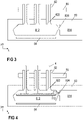
- FIG. 3 a device for forming a housing for a power semiconductor module arrangement according to one example is schematically illustrated.
- the device comprises a mold 80.
- a first cavity 812 is formed in the mold 80.
- the first cavity 812 comprises a plurality of first openings 822 and a second opening 824.
- the second opening 824 is coupled to a runner system 814 that is configured to inject a mold material 90 into the first cavity 812.
- Mold material 90 can be inserted into the first cavity 812 through more than one second opening 824 coupled to the runner system 814, for example.
- Each of the first openings 822 forms a connection from the first cavity 812 to the outside of the mold.
- a sleeve or hollow bushing 82 is inserted into each of the first openings 822.
- the device further comprises a cooling device 86 that is configured to cool the sleeves or hollow bushings 82, and a heating device 84 that is configured to heat the mold 80.
- a molded housing can be produced by means of the device illustrated in Figure 3 . That is, in contrast to the housing 7 that has been explained with respect to Figure 1 above, the housing produced with the device of Figure 3 does not comprise sidewalls and a cover, and a casting compound arranged inside the cavity formed by the sidewalls and the cover.
- the housing that can be formed with the device of Figure 3 instead is a compact housing, and a semiconductor module arrangement is molded directly into the housing. This will be explained in further detail below.
- a substrate 10 can be arranged inside the first cavity 812 of the mold 80.
- the substrate 10 can be similar to the substrate 10 that has been described with respect to Figure 1 above.
- Semiconductor bodies 20, connection layers 30 or electrical connections 3, however, are not specifically illustrated in Figure 4 .
- a plurality of terminal elements 4 is arranged on the substrate 10. Each of the terminal elements 4 protrudes through one of the plurality of sleeves or hollow bushings 82 to the outside of the first cavity 812 and the outside of the mold 80.
- the downholder 88 comprises a plurality of springs 886 arranged between a first plate 882 and one of a plurality of second plates 884.
- Each of the plurality of second plates 884 is configured to contact one of the plurality of terminal elements 4. That is, the first plate 882 exerts a pressure on the plurality of springs 886 and each of the plurality of springs 886 exerts a pressure on one of the plurality of second plates 884 which is transferred to the terminal elements 4. In this way, a certain pressure can be exerted on the terminal elements 4 in order to press them on the substrate 10.
- a downholder 88 can be implemented in any other suitable way.
- the first cavity 812 and the second cavity 814 are filled with a mold material 90.
- the mold material 90 inside the first cavity 812 forms the housing of the power semiconductor module arrangement.
- the first cavity 812 therefore, can have the desired form of the housing that is to be produced.
- the housing can be easily formed by pressing the mold material 90 into the first cavity 812 and subsequently hardening the mold material 90.
- the mold material When filling the mold material 90 into the first cavity 812, the mold material is liquid or viscous.
- the sleeves or hollow bushings 82 form openings of the first cavity 812 through which mold material 90 can leak out of the first cavity 812. Leakage of the mold material 90 through the sleeves or hollow bushings 82, however, is prevented by means of the cooling device 86.
- the cooling device 86 is configured to cool the sleeves or hollow bushings 82.
- the mold material 90 is usually heated to a certain degree when pressing it into the first cavity 812 in order to keep it liquid or viscous.
- the mold 80 is heated by means of the heating device 84. This prevents the mold material 90 from hardening too early in order to be able to completely fill the first cavity 812 without the formation of any unwanted voids. However, when the mold material 90 comes into contact with the cooled sleeves or hollow bushings 82, it will cool down and seal the openings 822, thereby preventing the mold material 90 from leaking out of the first cavity 812.
- Figure 6A schematically illustrates a cross-sectional view of a section of the mold 80.
- Figure 6A only one of the openings 822 is illustrated.
- the substrate 10 is partly visible in Figure 6A .
- the mold material 90 is pressed into the first cavity 812.
- the bold arrow indicates the direction of movement of the mold material 90.
- the mold material 90 is pressed further into the first cavity 812. When it comes into contact with the cooled sleeve or hollow bushing, it hardens and seals the opening 822.
- Figure 6C schematically illustrates a section of the mold 80 when the mold 80 is completely filled with the mold material 90.
- the semiconductor substrate arrangement is then molded into the mold material 90 and the mold material can be hardened. After hardening the mold material 90, the mold 80 can be removed.
- each of the plurality of sleeves or hollow bushings 82 can comprise a funnel-shaped end 92 directed towards the first cavity 812.
- the surface of the sleeve or hollow bushings 82 can be increased in that area where the mold material 90 comes into contact with the sleeve or hollow bushing 82. This allows to more rapidly cool down the mold material in the vicinity of the sleeve or hollow bushing, thereby effectively sealing the opening 822 and preventing the mold material 90 from leaking out of the first cavity 812.
- the mold material 90 only hardens in those sections arranged inside the funnel-shaped ends 92.
- Figure 7 schematically illustrates a cross-sectional view of a semiconductor substrate 10 molded into a housing that has been produced by means of the device explained with respect to Figures 3 to 6 above.
- the housing has the form of the first cavity 812.
- On a top surface of the housing a plurality of projections is visible. These projections result from the mold material 90 hardening in the range of the funnel-shaped ends 92 of the sleeves or hollow bushings 82.
- the sleeves or hollow bushings 82 can comprise a thermally conductive material such as, e.g., metal.
- the sleeves or hollow bushings 82 comprise copper. This allows to arrange the cooling device such that it contacts an end of the sleeves or hollow bushings 82 which is arranged outside the first cavity 812 and to still cool down the other end of the sleeves or hollow bushings 82 that is arranged adjacent to the first cavity 812.
- the mold 80 can be heated up to a temperature of between 150°C and 200°C, e.g., 180°C.
- the sleeves or hollow bushings 82 can be cooled down to a temperature of between 0°C and 50°C, e.g., to room temperature.
- the mold material 90 can be liquefied at temperatures of between 150°C and 200°C and can be hardened at temperatures between 0°C and 50°C. The temperatures generally depend on the kind of mold material 90 that is used to form the housing.
- the mold material 90 can comprise a thermoset or elastomer, for example.
- the cooling element 86 can be a water cooled cooling element, for example.
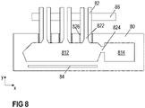
- FIG. 8 a cross-sectional view of a device for producing a housing for a power semiconductor module arrangement according to another example is schematically illustrated.
- the device generally corresponds to the device that has been described with respect to Figure 3 above.
- each of the sleeves or hollow bushings 82 is thermally isolated from the mold 80.
- the sleeves or hollow bushings 82 are cooled down, while the mold 80 is heated, when the mold material 90 is pressed into the first cavity 812.
- a thermal isolation 826 may be inserted between each of the sleeves or hollow bushings 82 and the mold 80.
- the thermal isolation 826 can comprise a layer of a thermally isolating material such as, e.g., Teflon. This, however, is only an example. Any other thermally isolating materials can be used instead. Instead of a layer of a thermally isolating material, the thermal isolation 826 can also comprise an air filled chamber. The air inside the chamber also has a thermally isolating effect. When arranging the thermal isolation 826 between the sleeves or hollow bushings 82 and the mold, a direct contact between the sleeves or hollow bushings 82 and the mold is avoided or at least reduced.
- a thermally isolating material such as, e.g., Teflon.
Landscapes
- Engineering & Computer Science (AREA)
- Mechanical Engineering (AREA)
- Physics & Mathematics (AREA)
- Health & Medical Sciences (AREA)
- Oral & Maxillofacial Surgery (AREA)
- Thermal Sciences (AREA)
- Encapsulation Of And Coatings For Semiconductor Or Solid State Devices (AREA)
- Cooling Or The Like Of Semiconductors Or Solid State Devices (AREA)
Abstract
Description
- The instant disclosure relates to a method and a device for producing a housing, in particular a housing for a power semiconductor module arrangement.
- Power semiconductor module arrangements often include at least one semiconductor substrate arranged in a housing. A semiconductor arrangement including a plurality of controllable semiconductor elements (e.g., two IGBTs in a half-bridge configuration) is arranged on each of the at least one substrate. Each substrate usually comprises a substrate layer (e.g., a ceramic layer), a first metallization layer deposited on a first side of the substrate layer and a second metallization layer deposited on a second side of the substrate layer. The controllable semiconductor elements are mounted, for example, on the first metallization layer. The second metallization layer may optionally be attached to a base plate. The controllable semiconductor devices are usually mounted to the semiconductor substrate by soldering or sintering techniques.
- There is a need for a method and a device that allow to easily and cost-effectively produce a housing for a power semiconductor module arrangement.
- A device for forming a housing for a power semiconductor module arrangement includes a mold. The mold includes a first cavity including a plurality of first openings and a second opening, the second opening being coupled to a runner system, wherein the runner system is configured to inject a mold material into the first cavity through the second opening. The device further includes a plurality of sleeves or hollow bushings, wherein a first end of each of the plurality of sleeves or hollow bushings is arranged in one of the first openings, and wherein a second end of each of the plurality of sleeves or hollow bushings extends to the outside of the mold, a heating element configured to heat the mold, and a cooling element configured to cool the plurality of sleeves or hollow bushings.
- A method includes arranging a power semiconductor module arrangement in the first cavity of a device for forming a housing for a power semiconductor module arrangement, arranging one of a plurality of terminal elements in each of the plurality of sleeves or hollow bushings such that a first end of each of the terminal elements contacts the power semiconductor module arrangement, and a second end of each of the terminal elements protrudes through the respective sleeve or hollow bushing and out of the mold, heating a mold material and pressing the mold material into the first cavity, and cooling the plurality of sleeves or hollow bushings by means of the cooling element, wherein the mold material hardens in the vicinity of the first ends of the plurality of sleeves or hollow bushings when it comes into contact with the respective first end, thereby sealing the second openings of the first cavity.
- The invention may be better understood with reference to the following drawings and the description. The components in the figures are not necessarily to scale, emphasis instead being placed upon illustrating the principles of the invention. Moreover, in the figures, like referenced numerals designate corresponding parts throughout the different views.
-
-
Figure 1 is a cross-sectional view of a power semiconductor module arrangement. -
Figure 2 is a diagonal view of a power semiconductor module arrangement. -
Figure 3 is a cross-sectional view of a device for producing a housing for a power semiconductor module arrangement according to one example. -
Figure 4 is a cross-sectional view of the device for producing a housing for a power semiconductor module arrangement ofFigure 3 after the insertion of terminal elements. -
Figure 5 is a cross-sectional view of the device for producing a housing for a power semiconductor module arrangement ofFigure 4 after the insertion of a mold material. -
Figure 6 , comprisingFigures 6A - 6C schematically illustrates a method for forming a housing for a power semiconductor module arrangement. -
Figure 7 is a cross-sectional view of a power semiconductor module arrangement molded into a housing. -
Figure 8 is a cross-sectional view of a device for producing a housing for a power semiconductor module arrangement according to another example. - In the following detailed description, reference is made to the accompanying drawings. The drawings show specific examples in which the invention may be practiced. It is to be understood that the features and principles described with respect to the various examples may be combined with each other, unless specifically noted otherwise. In the description, as well as in the claims, designations of certain elements as "first element", "second element", "third element" etc. are not to be understood as enumerative. Instead, such designations serve solely to address different "elements". That is, e.g., the existence of a "third element" does not require the existence of a "first element" and a "second element". An electrical line or electrical connection as described herein may be a single electrically conductive element, or include at least two individual electrically conductive elements connected in series and/or parallel. Electrical lines and electrical connections may include metal and/or semiconductor material, and may be permanently electrically conductive (i.e., non-switchable). A semiconductor body as described herein may be made from (doped) semiconductor material and may be a semiconductor chip or be included in a semiconductor chip. A semiconductor body has electrically connecting pads and includes at least one semiconductor element with electrodes.
- Referring to
Figure 1 , a cross-sectional view of a powersemiconductor module arrangement 100 is illustrated. The powersemiconductor module arrangement 100 includes ahousing 7 and a semiconductor substrate 10. The semiconductor substrate 10 includes a dielectric insulation layer 11, a (structured) first metallization layer 111 attached to the dielectric insulation layer 11, and a (structured)second metallization layer 112 attached to the dielectric insulation layer 11. The dielectric insulation layer 11 is disposed between the first andsecond metallization layers 111, 112. According to another example, thesecond metallization layer 112 can also be omitted. - Each of the first and
second metallization layers 111, 112 may consist of or include one of the following materials: copper; a copper alloy; aluminum; an aluminum alloy; any other metal or alloy that remains solid during the operation of the power semiconductor module arrangement. The semiconductor substrate 10 may be a ceramic substrate, that is, a substrate in which the dielectric insulation layer 11 is a ceramic, e.g., a thin ceramic layer. The ceramic may consist of or include one of the following materials: aluminum oxide; aluminum nitride; zirconium oxide; silicon nitride; boron nitride; or any other dielectric ceramic. For example, the dielectric insulation layer 11 may consist of or include one of the following materials: Al2O3, AlN, SiC, BeO or Si3N4. For instance, the substrate 10 may, e.g., be a Direct Copper Bonding (DCB) substrate, a Direct Aluminum Bonding (DAB) substrate, or an Active Metal Brazing (AMB) substrate. Further, the substrate 10 may be an Insulated Metal Substrate (IMS). An Insulated Metal Substrate generally comprises a dielectric insulation layer 11 comprising (filled) materials such as epoxy resin or polyimide, for example. The material of the dielectric insulation layer 11 may be filled with ceramic particles, for example. Such particles may comprise, e.g., Si2O, Al2O3, AlN, or BN and may have a diameter of between about 1µm and about 50µm. The substrate 10 may also be a conventional printed circuit board (PCB) having a non-ceramic dielectric insulation layer 11. For instance, a non-ceramic dielectric insulation layer 11 may consist of or include a cured resin. - The semiconductor substrate 10 is arranged in a
housing 7. In the example illustrated inFigure 1 , the semiconductor substrate 10 forms a ground surface of thehousing 7, while thehousing 7 itself solely comprises sidewalls and a cover. This is, however, only an example. It is also possible that thehousing 7 further comprises a ground surface and the semiconductor substrate 10 be arranged inside thehousing 7. According to another example, the semiconductor substrate 10 may be mounted on a base plate (not illustrated). In some powersemiconductor module arrangements 100, more than one semiconductor substrate 10 is arranged on a single base plate. The base plate may form a ground surface of thehousing 7, for example. - One or
more semiconductor bodies 20 may be arranged on the semiconductor substrate 10. Each of thesemiconductor bodies 20 arranged on the semiconductor substrate 10 may include a diode, an IGBT (Insulated-Gate Bipolar Transistor), a MOSFET (Metal-Oxide-Semiconductor Field-Effect Transistor), a JFET (Junction Field-Effect Transistor), a HEMT (High-Electron-Mobility Transistor), or any other suitable controllable semiconductor element. - The one or
more semiconductor bodies 20 may form a semiconductor arrangement on the semiconductor substrate 10. InFigure 1 , only twosemiconductor bodies 20 are exemplarily illustrated. Thesecond metallization layer 112 of the semiconductor substrate 10 inFigure 1 is a continuous layer. The first metallization layer 111 is a structured layer in the example illustrated inFigure 1 . "Structured layer" means that the first metallization layer 111 is not a continuous layer, but includes recesses between different sections of the layer. Such recesses are schematically illustrated inFigure 1 . The first metallization layer 111 in this example includes three different sections.Different semiconductor bodies 20 may be mounted to the same or to different sections of the first metallization layer 111. Different sections of the first metallization layer may have no electrical connection or may be electrically connected to one or more other sections using, e.g.,bonding wires 3.Electrical connections 3 may also include connection plates or conductor rails, for example, to name just a few examples. The one ormore semiconductor bodies 20 may be electrically and mechanically connected to the semiconductor substrate 10 by an electricallyconductive connection layer 30. Such an electrically conductive connection layer may be a solder layer, a layer of an electrically conductive adhesive, or a layer of a sintered metal powder, e.g., a sintered silver powder, for example. - The power
semiconductor module arrangement 100 illustrated inFigure 1 further includesterminal elements 4. Theterminal elements 4 are electrically connected to the first metallization layer 111 and provide an electrical connection between the inside and the outside of thehousing 7. Theterminal elements 4 may be electrically connected to the first metallization layer 111 with a first end, while asecond end 41 of theterminal elements 4 protrudes through anopening 722 and out of thehousing 7. Theterminal elements 4 may be electrically contacted from the outside at theirsecond end 41. Theterminal elements 4 illustrated inFigure 1 , however, are only examples.Terminal elements 4 may be implemented in any other way and may be arranged anywhere within thehousing 7. For example, one or moreterminal elements 4 may be arranged close to or adjacent to the sidewalls of thehousing 7.Terminal elements 4 can also extend vertically or horizontally through the sidewalls of thehousing 7, for example. Any other suitable implementation is possible. - Conventional power
semiconductor module arrangements 100 generally further include a castingcompound 5. The castingcompound 5 may consist of or include a silicone gel or may be a rigid molding compound, for example. The castingcompound 5 may at least partly fill the interior of thehousing 7, thereby covering the components and electrical connections that are arranged on the semiconductor substrate 10. Theterminal elements 4 may be partly embedded in the castingcompound 5. At least their second ends 41, however, are not covered by the castingcompound 5 and protrude from the castingcompound 5 through thehousing 7 to the outside of thehousing 7. The castingcompound 5 is configured to protect the components and electrical connections inside thepower semiconductor module 100, in particular inside thehousing 7, from certain environmental conditions and mechanical damage. The castingcompound 5 further provides for an electrical isolation of the components inside thehousing 7. - Now referring to
Figure 2 , a diagonal view of a power semiconductor module arrangement is schematically illustrated. In this diagonal view the substrate 10 inside thehousing 7 with thesemiconductor bodies 20 mounted thereon is not visible. Visible are only theopenings 722 in thehousing 7 and the second ends 41 of theterminal elements 4 protruding out of thehousing 7. - Producing the power
semiconductor module arrangement 100 that has been explained with respect toFigures 1 and 2 above can be elaborate and costly. Now referring toFigure 3 , a device for forming a housing for a power semiconductor module arrangement according to one example is schematically illustrated. The device comprises amold 80. Afirst cavity 812 is formed in themold 80. Thefirst cavity 812 comprises a plurality offirst openings 822 and asecond opening 824. Thesecond opening 824 is coupled to arunner system 814 that is configured to inject amold material 90 into thefirst cavity 812. This, however, is only an example.Mold material 90 can be inserted into thefirst cavity 812 through more than onesecond opening 824 coupled to therunner system 814, for example. Each of thefirst openings 822 forms a connection from thefirst cavity 812 to the outside of the mold. - A sleeve or
hollow bushing 82 is inserted into each of thefirst openings 822. The device further comprises acooling device 86 that is configured to cool the sleeves orhollow bushings 82, and aheating device 84 that is configured to heat themold 80. A molded housing can be produced by means of the device illustrated inFigure 3 . That is, in contrast to thehousing 7 that has been explained with respect toFigure 1 above, the housing produced with the device ofFigure 3 does not comprise sidewalls and a cover, and a casting compound arranged inside the cavity formed by the sidewalls and the cover. The housing that can be formed with the device ofFigure 3 instead is a compact housing, and a semiconductor module arrangement is molded directly into the housing. This will be explained in further detail below. - Now referring to
Figure 4 , a substrate 10 can be arranged inside thefirst cavity 812 of themold 80. The substrate 10 can be similar to the substrate 10 that has been described with respect toFigure 1 above.Semiconductor bodies 20, connection layers 30 orelectrical connections 3, however, are not specifically illustrated inFigure 4 . A plurality ofterminal elements 4 is arranged on the substrate 10. Each of theterminal elements 4 protrudes through one of the plurality of sleeves orhollow bushings 82 to the outside of thefirst cavity 812 and the outside of themold 80. - Now referring to
Figure 5 , it is optionally possible to press theterminal elements 4 towards the substrate 10 by means of adownholder 88. In the example illustrated inFigure 5 , thedownholder 88 comprises a plurality ofsprings 886 arranged between afirst plate 882 and one of a plurality ofsecond plates 884. Each of the plurality ofsecond plates 884 is configured to contact one of the plurality ofterminal elements 4. That is, thefirst plate 882 exerts a pressure on the plurality ofsprings 886 and each of the plurality ofsprings 886 exerts a pressure on one of the plurality ofsecond plates 884 which is transferred to theterminal elements 4. In this way, a certain pressure can be exerted on theterminal elements 4 in order to press them on the substrate 10. The pressure, however, can be limited to a maximum value due to the flexibility of thesprings 886. In this way damages to theterminal elements 4 and the substrate 10 when pressing theterminal elements 4 on the substrate 10 can be prevented. This, however, is only one example. Adownholder 88 can be implemented in any other suitable way. In the example illustrated inFigure 5 , thefirst cavity 812 and thesecond cavity 814 are filled with amold material 90. Themold material 90 inside thefirst cavity 812 forms the housing of the power semiconductor module arrangement. Thefirst cavity 812, therefore, can have the desired form of the housing that is to be produced. - As will be further described with respect to
Figure 6 below, the housing can be easily formed by pressing themold material 90 into thefirst cavity 812 and subsequently hardening themold material 90. When filling themold material 90 into thefirst cavity 812, the mold material is liquid or viscous. The sleeves orhollow bushings 82, however, form openings of thefirst cavity 812 through whichmold material 90 can leak out of thefirst cavity 812. Leakage of themold material 90 through the sleeves orhollow bushings 82, however, is prevented by means of thecooling device 86. Thecooling device 86 is configured to cool the sleeves orhollow bushings 82. Themold material 90 is usually heated to a certain degree when pressing it into thefirst cavity 812 in order to keep it liquid or viscous. In order to be able to completely fill thefirst cavity 812 with themold material 90, themold 80 is heated by means of theheating device 84. This prevents themold material 90 from hardening too early in order to be able to completely fill thefirst cavity 812 without the formation of any unwanted voids. However, when themold material 90 comes into contact with the cooled sleeves orhollow bushings 82, it will cool down and seal theopenings 822, thereby preventing themold material 90 from leaking out of thefirst cavity 812. - This will be explained in further detail with respect to
Figure 6 .Figure 6A schematically illustrates a cross-sectional view of a section of themold 80. InFigure 6A only one of theopenings 822 is illustrated. The substrate 10 is partly visible inFigure 6A . Themold material 90 is pressed into thefirst cavity 812. The bold arrow indicates the direction of movement of themold material 90. Now referring toFigure 6B , themold material 90 is pressed further into thefirst cavity 812. When it comes into contact with the cooled sleeve or hollow bushing, it hardens and seals theopening 822. However, as themold 80 is heated by means of the heating device 84 (not visible inFigure 6 ), it only hardens in direct vicinity of the sleeve orhollow bushing 82 and remains liquid or viscous in all other parts. In this way, themold material 90 can be pressed even further into the first cavity, as indicated by the bold arrow inFigure 6B .Figure 6C schematically illustrates a section of themold 80 when themold 80 is completely filled with themold material 90. The semiconductor substrate arrangement is then molded into themold material 90 and the mold material can be hardened. After hardening themold material 90, themold 80 can be removed. - Still referring to
Figure 6 , each of the plurality of sleeves orhollow bushings 82 can comprise a funnel-shapedend 92 directed towards thefirst cavity 812. In this way, the surface of the sleeve orhollow bushings 82 can be increased in that area where themold material 90 comes into contact with the sleeve orhollow bushing 82. This allows to more rapidly cool down the mold material in the vicinity of the sleeve or hollow bushing, thereby effectively sealing theopening 822 and preventing themold material 90 from leaking out of thefirst cavity 812. According to one example, themold material 90 only hardens in those sections arranged inside the funnel-shaped ends 92. -
Figure 7 schematically illustrates a cross-sectional view of a semiconductor substrate 10 molded into a housing that has been produced by means of the device explained with respect toFigures 3 to 6 above. The housing has the form of thefirst cavity 812. On a top surface of the housing, a plurality of projections is visible. These projections result from themold material 90 hardening in the range of the funnel-shaped ends 92 of the sleeves orhollow bushings 82. - According to one example, the sleeves or
hollow bushings 82 can comprise a thermally conductive material such as, e.g., metal. According to one example, the sleeves orhollow bushings 82 comprise copper. This allows to arrange the cooling device such that it contacts an end of the sleeves orhollow bushings 82 which is arranged outside thefirst cavity 812 and to still cool down the other end of the sleeves orhollow bushings 82 that is arranged adjacent to thefirst cavity 812. Themold 80 can be heated up to a temperature of between 150°C and 200°C, e.g., 180°C. The sleeves orhollow bushings 82 can be cooled down to a temperature of between 0°C and 50°C, e.g., to room temperature. Themold material 90 can be liquefied at temperatures of between 150°C and 200°C and can be hardened at temperatures between 0°C and 50°C. The temperatures generally depend on the kind ofmold material 90 that is used to form the housing. Themold material 90 can comprise a thermoset or elastomer, for example. Thecooling element 86 can be a water cooled cooling element, for example. - Now referring to
Figure 8 , a cross-sectional view of a device for producing a housing for a power semiconductor module arrangement according to another example is schematically illustrated. The device generally corresponds to the device that has been described with respect toFigure 3 above. In the example illustrated inFigure 8 , however, each of the sleeves orhollow bushings 82 is thermally isolated from themold 80. As has been described above, the sleeves orhollow bushings 82 are cooled down, while themold 80 is heated, when themold material 90 is pressed into thefirst cavity 812. In order to keep both the sleeves orhollow bushings 82 and themold 80 at the desired temperature, athermal isolation 826 may be inserted between each of the sleeves orhollow bushings 82 and themold 80. Thethermal isolation 826 can comprise a layer of a thermally isolating material such as, e.g., Teflon. This, however, is only an example. Any other thermally isolating materials can be used instead. Instead of a layer of a thermally isolating material, thethermal isolation 826 can also comprise an air filled chamber. The air inside the chamber also has a thermally isolating effect. When arranging thethermal isolation 826 between the sleeves orhollow bushings 82 and the mold, a direct contact between the sleeves orhollow bushings 82 and the mold is avoided or at least reduced.
Claims (15)
- A device for forming a housing for a power semiconductor module arrangement comprises a mold (80), wherein the mold (80) comprises:a first cavity (812) comprising a plurality of first openings (822) and a second opening (824), the second opening being coupled to a runner system (814), wherein the runner system (814) is configured to inject a mold material (90) into the first cavity (812) through the second opening (824);a plurality of sleeves or hollow bushings (82), wherein a first end (92) of each of the plurality of sleeves or hollow bushings (82) is arranged in one of the first openings (822), and wherein a second end of each of the plurality of sleeves or hollow bushings (82) extends to the outside of the mold (80);a heating element (84) configured to heat the mold (80); anda cooling element (86) configured to cool the plurality of sleeves or hollow bushings (82).
- The device of claim 1, wherein the cooling element (86) is coupled to the second end of each of the plurality of sleeves or hollow bushings (82).
- The device of claim 1 or 2, wherein each of the plurality of sleeves or hollow bushings (82) comprises a heat conducting material.
- The device of claim 3, wherein each of the plurality of sleeves or hollow bushings (82) comprises a metal.
- The device of any of the preceding claims, wherein the first cavity (812) comprises the form of the housing that is to be formed.
- The device of any of the preceding claims, further comprising a downholder (88), wherein the downholder (88) is configured to, when a semiconductor module arrangement is arranged in the first cavity (812) and one of a plurality of terminal elements (4) is arranged in a different one of the plurality of sleeves or hollow bushings (82), press the plurality of terminal elements (4) on the power semiconductor module arrangement.
- The device of claim 6, wherein the downholder (88) comprises a plurality of springs (886) arranged between a first plate (882) and one of a plurality of second plates (884), wherein each of the plurality of second plates (884) is configured to contact one of the plurality of terminal elements (4).
- The device of any of the preceding claims, wherein the heating element (84) is configured to heat the mold (80) to a temperature of between 150°C and 200°C, and wherein the cooling element (86) is configured to cool the plurality of sleeves or hollow bushings (82) to a temperature of between 0°C and 50°C.
- The device of any of the preceding claims, wherein the cooling element (86) is a water cooled cooling element.
- The device of any of the preceding claims, wherein the first ends (92) of the plurality of sleeves or hollow bushings (82) are funnel-shaped.
- The device of any of the preceding claims, further comprising a plurality of thermal isolations (826), wherein each thermal isolation (826) is arranged between a different one of the plurality of sleeves or hollow bushings (82) and the mold (80) and is configured to thermally isolate the respective sleeve or hollow bushing (82) from the mold (80).
- The device of claim 11, wherein each of the plurality of thermal isolations (826) comprises a layer of a thermally isolating material or an air filled chamber.
- A method comprising:arranging a power semiconductor module arrangement in the first cavity (812) of a device according to any of claims 1 to 12;arranging one of a plurality of terminal elements (4) in each of the plurality of sleeves or hollow bushings (82) such that a first end of each of the terminal elements (4) contacts the power semiconductor module arrangement, and a second end of each of the terminal elements (4) protrudes through the respective sleeve or hollow bushing (82) and out of the mold (80);heating a mold material (90) and pressing the mold material (90) into the first cavity (812); andcooling the plurality of sleeves or hollow bushings (82) by means of the cooling element (86), whereinthe mold material (90) hardens in the vicinity of the first ends of the plurality of sleeves or hollow bushings (82) when it comes into contact with the respective first end, thereby sealing the second openings (822) of the first cavity (812).
- The method of claim 13, further comprising, after completely filling the first cavity (812) with the mold material (90), hardening the mold material (90).
- The method of claim 13 or 14, further comprising, while pressing the mold material (90) into the first cavity (812), pressing the plurality of terminal elements (4) on the power semiconductor module arrangement.
Priority Applications (3)
| Application Number | Priority Date | Filing Date | Title |
|---|---|---|---|
| EP21160985.4A EP4053887B1 (en) | 2021-03-05 | 2021-03-05 | Method and device for producing a housing |
| US17/685,870 US12261063B2 (en) | 2021-03-05 | 2022-03-03 | Method and device for producing a housing |
| CN202210207260.0A CN115008762A (en) | 2021-03-05 | 2022-03-04 | Method and device for producing a housing |
Applications Claiming Priority (1)
| Application Number | Priority Date | Filing Date | Title |
|---|---|---|---|
| EP21160985.4A EP4053887B1 (en) | 2021-03-05 | 2021-03-05 | Method and device for producing a housing |
Publications (2)
| Publication Number | Publication Date |
|---|---|
| EP4053887A1 true EP4053887A1 (en) | 2022-09-07 |
| EP4053887B1 EP4053887B1 (en) | 2026-04-29 |
Family
ID=74859699
Family Applications (1)
| Application Number | Title | Priority Date | Filing Date |
|---|---|---|---|
| EP21160985.4A Active EP4053887B1 (en) | 2021-03-05 | 2021-03-05 | Method and device for producing a housing |
Country Status (3)
| Country | Link |
|---|---|
| US (1) | US12261063B2 (en) |
| EP (1) | EP4053887B1 (en) |
| CN (1) | CN115008762A (en) |
Families Citing this family (1)
| Publication number | Priority date | Publication date | Assignee | Title |
|---|---|---|---|---|
| US20240222240A1 (en) * | 2023-01-04 | 2024-07-04 | Hyundai Mobis Co., Ltd. | Power semiconductor module and method of manufacturing the same |
Citations (6)
| Publication number | Priority date | Publication date | Assignee | Title |
|---|---|---|---|---|
| CN101740527A (en) * | 2008-11-21 | 2010-06-16 | 乾坤科技股份有限公司 | Chip packaging structure and manufacturing method thereof |
| JP2011077280A (en) * | 2009-09-30 | 2011-04-14 | Mitsubishi Electric Corp | Power semiconductor device and method of manufacturing the same |
| JP2011165836A (en) * | 2010-02-09 | 2011-08-25 | Mitsubishi Electric Corp | Power semiconductor device |
| JP5082687B2 (en) * | 2007-08-30 | 2012-11-28 | オムロン株式会社 | Transfer mold type power module |
| US20170236782A1 (en) * | 2016-02-16 | 2017-08-17 | Fuji Electric Co., Ltd. | Semiconductor module manufacturing method and semiconductor module |
| US20200350236A1 (en) * | 2018-12-19 | 2020-11-05 | Shindengen Electric Manufacturing Co., Ltd. | Semiconductor device and semiconductor device manufacturing method |
Family Cites Families (5)
| Publication number | Priority date | Publication date | Assignee | Title |
|---|---|---|---|---|
| JP2002072024A (en) * | 2000-08-31 | 2002-03-12 | Hitachi Ltd | Optical semiconductor package manufacturing method and optical semiconductor coupling device |
| JP5345017B2 (en) * | 2009-08-27 | 2013-11-20 | 三菱電機株式会社 | Power semiconductor device and manufacturing method thereof |
| US20130015567A1 (en) * | 2010-10-21 | 2013-01-17 | Panasonic Corporation | Semiconductor device and production method for same |
| WO2015040490A2 (en) * | 2013-09-19 | 2015-03-26 | Magna International Inc. | High-pressure die casting apparatus and method |
| KR20150060036A (en) | 2013-11-25 | 2015-06-03 | 삼성전기주식회사 | Power Semi-conductor module and Method of the Manufacturing the same |
-
2021
- 2021-03-05 EP EP21160985.4A patent/EP4053887B1/en active Active
-
2022
- 2022-03-03 US US17/685,870 patent/US12261063B2/en active Active
- 2022-03-04 CN CN202210207260.0A patent/CN115008762A/en active Pending
Patent Citations (6)
| Publication number | Priority date | Publication date | Assignee | Title |
|---|---|---|---|---|
| JP5082687B2 (en) * | 2007-08-30 | 2012-11-28 | オムロン株式会社 | Transfer mold type power module |
| CN101740527A (en) * | 2008-11-21 | 2010-06-16 | 乾坤科技股份有限公司 | Chip packaging structure and manufacturing method thereof |
| JP2011077280A (en) * | 2009-09-30 | 2011-04-14 | Mitsubishi Electric Corp | Power semiconductor device and method of manufacturing the same |
| JP2011165836A (en) * | 2010-02-09 | 2011-08-25 | Mitsubishi Electric Corp | Power semiconductor device |
| US20170236782A1 (en) * | 2016-02-16 | 2017-08-17 | Fuji Electric Co., Ltd. | Semiconductor module manufacturing method and semiconductor module |
| US20200350236A1 (en) * | 2018-12-19 | 2020-11-05 | Shindengen Electric Manufacturing Co., Ltd. | Semiconductor device and semiconductor device manufacturing method |
Also Published As
| Publication number | Publication date |
|---|---|
| EP4053887B1 (en) | 2026-04-29 |
| US12261063B2 (en) | 2025-03-25 |
| CN115008762A (en) | 2022-09-06 |
| US20220285178A1 (en) | 2022-09-08 |
Similar Documents
| Publication | Publication Date | Title |
|---|---|---|
| CN107665867B (en) | Double-encapsulated power semiconductor module and method for producing same | |
| EP3929973B1 (en) | A power semiconductor module and a method for producing a power semiconductor module | |
| US12500152B2 (en) | Power semiconductor module, method for assembling a power semiconductor module and housing for a power semiconductor module | |
| US11699625B2 (en) | Power semiconductor module arrangement | |
| US11581230B2 (en) | Power semiconductor module and a method for producing a power semiconductor module | |
| CN108353511B (en) | Electronic module and method for manufacturing electronic module | |
| EP3859775A1 (en) | Semiconductor arrangement and method for producing the same | |
| US12564094B2 (en) | Power semiconductor module arrangement and method for producing the same | |
| US12261063B2 (en) | Method and device for producing a housing | |
| EP4084062A1 (en) | Power semiconductor module arrangement | |
| US12456654B2 (en) | Power semiconductor modules | |
| EP4270469A1 (en) | Power semiconductor module | |
| EP4276888A1 (en) | Method for producing a power semiconductor module | |
| EP4604176A1 (en) | Semiconductor module arrangement, electronics carrier for a semiconductor module arrangement, and method for producing a semiconductor module arrangement | |
| EP4270466A1 (en) | Power semiconductor module arrangements and methods for producing power semiconductor module arrangements | |
| EP4651201A1 (en) | Power semiconductor module arrangement and methods for producing the same | |
| EP4227986A1 (en) | Power semiconductor module arrangement and methods for producing a semiconductor arrangement | |
| US20260090385A1 (en) | Semiconductor module comprising a housing | |
| EP4428914A1 (en) | Power semiconductor module arrangement | |
| EP3951866A1 (en) | Semiconductor substrate arrangement and method for producing the same | |
| CN119092418A (en) | Method for producing a seal for a semiconductor module and housing for a semiconductor module |
Legal Events
| Date | Code | Title | Description |
|---|---|---|---|
| PUAI | Public reference made under article 153(3) epc to a published international application that has entered the european phase |
Free format text: ORIGINAL CODE: 0009012 |
|
| STAA | Information on the status of an ep patent application or granted ep patent |
Free format text: STATUS: REQUEST FOR EXAMINATION WAS MADE |
|
| 17P | Request for examination filed |
Effective date: 20220127 |
|
| AK | Designated contracting states |
Kind code of ref document: A1 Designated state(s): AL AT BE BG CH CY CZ DE DK EE ES FI FR GB GR HR HU IE IS IT LI LT LU LV MC MK MT NL NO PL PT RO RS SE SI SK SM TR |
|
| GRAP | Despatch of communication of intention to grant a patent |
Free format text: ORIGINAL CODE: EPIDOSNIGR1 |
|
| STAA | Information on the status of an ep patent application or granted ep patent |
Free format text: STATUS: GRANT OF PATENT IS INTENDED |
|
| RIC1 | Information provided on ipc code assigned before grant |
Ipc: H01L 21/56 20060101AFI20251021BHEP Ipc: H01L 23/31 20060101ALN20251021BHEP Ipc: H01L 25/07 20060101ALN20251021BHEP Ipc: H01L 23/373 20060101ALN20251021BHEP |
|
| INTG | Intention to grant announced |
Effective date: 20251110 |
|
| GRAS | Grant fee paid |
Free format text: ORIGINAL CODE: EPIDOSNIGR3 |
|
| GRAA | (expected) grant |
Free format text: ORIGINAL CODE: 0009210 |
|
| STAA | Information on the status of an ep patent application or granted ep patent |
Free format text: STATUS: THE PATENT HAS BEEN GRANTED |
|
| AK | Designated contracting states |
Kind code of ref document: B1 Designated state(s): AL AT BE BG CH CY CZ DE DK EE ES FI FR GB GR HR HU IE IS IT LI LT LU LV MC MK MT NL NO PL PT RO RS SE SI SK SM TR |
|
| REG | Reference to a national code |
Ref country code: CH Ref legal event code: F10 Free format text: ST27 STATUS EVENT CODE: U-0-0-F10-F00 (AS PROVIDED BY THE NATIONAL OFFICE) Effective date: 20260429 Ref country code: GB Ref legal event code: FG4D |
|
| P01 | Opt-out of the competence of the unified patent court (upc) registered |
Free format text: CASE NUMBER: UPC_APP_0011512_4053887/2026 Effective date: 20260331 |