EP4053524A1 - Temperature measurement circuit with multiple distributed small low-power temperature sensors - Google Patents
Temperature measurement circuit with multiple distributed small low-power temperature sensors Download PDFInfo
- Publication number
- EP4053524A1 EP4053524A1 EP21160754.4A EP21160754A EP4053524A1 EP 4053524 A1 EP4053524 A1 EP 4053524A1 EP 21160754 A EP21160754 A EP 21160754A EP 4053524 A1 EP4053524 A1 EP 4053524A1
- Authority
- EP
- European Patent Office
- Prior art keywords
- temperature sensors
- local temperature
- measurement circuit
- processing unit
- circuit according
- Prior art date
- Legal status (The legal status is an assumption and is not a legal conclusion. Google has not performed a legal analysis and makes no representation as to the accuracy of the status listed.)
- Granted
Links
Images


Classifications
-
- G—PHYSICS
- G01—MEASURING; TESTING
- G01K—MEASURING TEMPERATURE; MEASURING QUANTITY OF HEAT; THERMALLY-SENSITIVE ELEMENTS NOT OTHERWISE PROVIDED FOR
- G01K1/00—Details of thermometers not specially adapted for particular types of thermometer
- G01K1/02—Means for indicating or recording specially adapted for thermometers
- G01K1/026—Means for indicating or recording specially adapted for thermometers arrangements for monitoring a plurality of temperatures, e.g. by multiplexing
-
- G—PHYSICS
- G01—MEASURING; TESTING
- G01K—MEASURING TEMPERATURE; MEASURING QUANTITY OF HEAT; THERMALLY-SENSITIVE ELEMENTS NOT OTHERWISE PROVIDED FOR
- G01K15/00—Testing or calibrating of thermometers
- G01K15/005—Calibration
-
- G—PHYSICS
- G01—MEASURING; TESTING
- G01K—MEASURING TEMPERATURE; MEASURING QUANTITY OF HEAT; THERMALLY-SENSITIVE ELEMENTS NOT OTHERWISE PROVIDED FOR
- G01K3/00—Thermometers giving results other than momentary value of temperature
- G01K3/08—Thermometers giving results other than momentary value of temperature giving differences of values; giving differentiated values
-
- G—PHYSICS
- G01—MEASURING; TESTING
- G01K—MEASURING TEMPERATURE; MEASURING QUANTITY OF HEAT; THERMALLY-SENSITIVE ELEMENTS NOT OTHERWISE PROVIDED FOR
- G01K7/00—Measuring temperature based on the use of electric or magnetic elements directly sensitive to heat ; Power supply therefor, e.g. using thermoelectric elements
- G01K7/01—Measuring temperature based on the use of electric or magnetic elements directly sensitive to heat ; Power supply therefor, e.g. using thermoelectric elements using semiconducting elements having PN junctions
- G01K7/015—Measuring temperature based on the use of electric or magnetic elements directly sensitive to heat ; Power supply therefor, e.g. using thermoelectric elements using semiconducting elements having PN junctions using microstructures, e.g. made of silicon
Definitions
- the present invention relates to a temperature measurement circuit integrated in a semiconductor chip, e.g. comprising a (large) integrated sensor circuit.
- Temperature sensors in integrated circuits are quite common to measure the environmental temperature of the chip and also to measure the temperature at different locations within the chip.
- the temperature sensor used is a Bipolar Junction Transistor (BJT) configured as a diode.
- BJT Bipolar Junction Transistor
- ADC Analog-to-Digital Convertor
- the present invention seeks to provide an improved temperature measurement circuit, which allows easy integration in an integrated circuit on a semiconductor chip, yet provides a high accuracy measurement result.
- a temperature measurement circuit as defined above is provided, comprising a plurality of local temperature sensors and a central processing unit connected to the plurality of local temperature sensors via respective integrated wiring structures in the semiconductor chip.
- the central processing unit comprises a control logic unit, and an analog-to-digital converter, ADC, circuit for providing digital measurement output data.
- the control logic unit is connected to the ADC circuit and arranged to select one or more of the plurality of local temperature sensors and execute a measurement cycle for the selected one or more of the plurality of local temperature sensors.
- the temperature measurement circuit further comprises a central temperature sensor connected to the central processing unit. This allows to further improve the accuracy of the temperature measurement circuit, as it allows to properly calibrate the plurality of local temperature sensors.
- the present invention embodiments described herein are especially applicable and useful for temperature measurement in semiconductor chips, notably those having a large sensor surface.
- the present invention embodiments of the temperature measurement circuit may be used inside a CMOS Image Sensor (CIS) chip.
- CIS CMOS Image Sensor
- the dark current generation in a CMOS image sensor is very important for image quality and is also very sensitive to the die temperature in different regions of the sensor array.
- cancellation methods are applied to remove the average dark current in the sensor array, but it is much more difficult when the temperature and corresponding dark current varies over the sensor array.
- By capturing the temperature at multiple locations on the die/ semiconductor chip it is possible to obtain knowledge on the thermal gradients on the die. This is useful to improve thermal gradients in future designs or to improve the package design for the existing product. It is also possible to use this information to perform a much more accurate dark current cancellation.
- the temperature is measured at different points on the die using multiple temperature sensors or sensor elements. The measured temperature and temperature distribution may be used to improve the image quality of the image (or video) captured by the image sensor.
- the application area of the present invention embodiments is useful in any CIS semiconductor chip where distributed temperature information is useful, or even any integrated semiconductor chip where this is an interesting problem (large, high power digital chips for example).
- Fig. 5A shows a top view of a semiconductor chip 20 in which exemplary embodiments of the present invention are illustrated.
- the semiconductor chip 20 comprises a semiconductor sensor circuit 21 and a further integrated circuit part 22, e.g. integrated signal processing electronics.
- a plurality of local temperature sensors 10 are present, located around a perimeter of the semiconductor sensor circuit 21, and connected to a central processing unit 1.
- the present invention relates to a temperature measurement circuit integrated in a semiconductor chip 20 comprising a plurality of local temperature sensors 10, and a central processing unit 1 connected to the plurality of local temperature sensors 10 via respective integrated wiring structures 15 in the semiconductor chip 20.
- the central processing unit 1 comprises a control logic unit 2 and an analog-to-digital converter, ADC, circuit 4-8 for providing digital measurement output data (see Fig. 4 and description thereof below for more details).
- the control logic unit 2 is connected to the ADC circuit 4-8 and arranged to select one or more of the plurality of local temperature sensors 10 and execute a measurement cycle for the selected one or more of the plurality of local temperature sensors 10.
- the temperature measurement circuit further comprises a central temperature sensor 11 connected to the central processing unit 1.
- a central temperature sensor 11 may be an integral part of (co-located) of the central processing unit 1 implemented in the semiconductor chip 20.
- This central temperature sensor 11 can be used to improve the accuracy of temperature measurements of the selected one or more of the plurality of local temperature sensors 10, e.g. by using a central temperature measurement for calibration purposes (see also further exemplary embodiments described below).
- FIG. 4 shows a schematic diagram of a central processing unit 1 as implemented in a further embodiment of the present invention, comprising the control logic unit 2, a reference circuit 9, a biasing unit 3, an ADC circuit (with input multiplexer 4, ramp generator 5, counter 6, counter latch 7 and comparator 8, to be discussed in further detail below), and an optional central temperature sensor 11. Also indicated in the Fig. 4 embodiment are the specific interconnections with signal names, and input and output signals, as used herein.
- a temperature sensor integrated in a semiconductor chip often is formed by a bipolar Junction Transistor (BJT) configured as a diode.
- BJT bipolar Junction Transistor
- ADC Analog-to-Digital Convertor
- the semiconductor chip To measure the temperature at different locations on the semiconductor chip, several temperature sensors are placed on the chip. If an ADC is applied for each temperature sensor present, the total area and power consumption of the collective temperature measurement circuits might increase rapidly. In the present invention embodiments, therefor one central ADC circuit 4-8 is used that can handle a multiple number of the plurality of local temperature sensors 10 integrated in the semiconductor chip 20.
- a simple BJT based temperature sensor has a potential accuracy problem.
- BJT based solutions have a large variable offset. In a production calibration process it is possible to measure this offset and store the associated data on the semiconductor chip. However, this limits the temperature sensor performance accuracy to the accuracy of the production calibration operation.
- the present invention embodiments provide a good mechanism to improve the temperature measurement performance, as will be discussed in further detail below.
- the BJT when the BJT is biased, it might emit light, which can be picked up by the semiconductor sensor circuit 21. This is, of course, something that needs to be avoided. Therefore, in the present invention embodiments, the BJT's are only biased when the semiconductor sensor circuit 21 is not capturing an image.
- the central processing unit 1 further comprises a bias circuit 3 connected to the plurality of local temperature sensors 10 and the control logic unit 2, wherein the central processing unit 1 is further arranged to execute a measurement cycle by providing a bias current from the bias circuit 3 to the selected one or more of the plurality of local temperature sensors 10, and measuring a sensor signal from the selected one or more of the plurality of local temperature sensors 10.
- a bias circuit 3 which supplies a predetermined bias current to the selected ones of the local temperature sensors 10 a more precise measurement is possible with limited additional circuitry integrated in the semiconductor chip 20.
- each of the plurality of local temperature sensors 10 comprises a bipolar junction transistor, BJT 10.
- BJT 10 bipolar junction transistor
- the BJT 10 is configured as a diode by a connection between base and collector, a bias input terminal ibias connected to an emitter of the BJT 10, a sense terminal vbe connected to the emitter of the BJT 10, a reference ground terminal refgnd connected to the base of the BJT 10, a first ground terminal agnd connected to the base of the BJT 10, and a second ground terminal subgnd connected to the collector of the BJT 10.
- the first ground terminal agnd and second ground terminal subgnd are connected together.
- the (PNP) Bipolar Junction Transistors 10 are configured as diode by connecting the base and collector to the same potential.
- a bias current ibias is steered into the emitter of the BJT 10 (but only when the specific BJT is selected to be measured by the ADC circuit 4-8.
- the diode voltage is then e.g. sampled onto a sampling capacitor and held during the ADC conversion.
- a 16-bit digital value is converted one by one into a 16-bit digital value, by an ADC circuit 4-8 in the form of a slope type of converter.
- Such a slope type of converter can be easily included in the central processing unit 1 on the semiconductor chip 20. Having the ADC circuit 4-8 embodied with a 16 bit resolution output provides for high accuracy measurement data.
- the bias current that is steered into the emitter of the BJT 10 is generated by the bias circuit 3.
- the bias current that is steered into the BJT 10 is derived from a reference current ibias_in provided by a reference circuit 9.
- the reference circuit 9 is e.g. implemented as a bandgap circuit in which a trimmed reference voltage and a trimmed bias is generated.
- the central processing unit 1 is further arranged to execute a calibration step for all of the plurality of local temperature sensors 10 during a production calibration mode of operation of the semiconductor chip 20. This obtains a central temperature sensor measurement circuit that provides high accuracy temperature data.
- the central temperature sensor 11 is used for the calibration process, allowing to determine the temperature of the semiconductor chip 20 more accurately. Obtaining a temperature measurement based on the central temperature sensor 11, and comparing that to the result returned by the plurality of local temperature sensors 10, it is possible to adjust for offset or related errors in the plurality of local temperature sensors 10.
- the temperature measurement circuit further comprises a central temperature sensor 11 connected to the central processing unit 1, wherein the calibration step includes a temperature measurement using the central temperature sensor 11.
- the central processing unit 1 is further arranged to execute a differential measurement cycle.
- the differential measurement cycle is e.g. based on measurement of two closely located local temperature sensors 10 with different temperature dependency characteristics (see below), or by using two different bias currents sequentially to one of the local temperature sensors 10.
- the central processing unit 1 is further arranged to execute a calibration step for all of the plurality of local temperature sensors 10 during a low power mode of operation of the semiconductor chip 20.
- a low power mode of operation of the semiconductor chip 20 In e.g. a CIS semiconductor chip 20, low power operating modes are present, and these can be used to repeat the calibration process during actual operation. In this way, the calibration can be performed at the actual ambient operating temperature of the semiconductor chip 20 which may be changing due to other power consuming activity in the system or due to environmental temperature changes. The accuracy will be improved by performing the calibration at a temperature closer to the semiconductor chip 20 operating temperature in a high power mode.
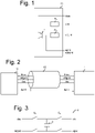
- Fig. 1 shows a circuit diagram of an embodiment of a local temperature sensor 10 as applied in present invention embodiments of the temperature measurement circuit.
- Each temperature sensor 10 is constructed by using a single PNP Bipolar Junction Transistor T.
- Each temperature sensor 10 has five terminals (or pins), i.e. an ibias pin connected to the emitter, vbe sense pin connected to the emitter, refgnd sense pin connected to the base, agnd pin connected to the base, and subgnd pin connected to the collector.
- a bias current can be input from the ibias pin into the emitter of the BJT T.
- the current returns via subgnd connected the collector and via agnd connected to the base of the BJT T.
- the agnd and subgnd will be connected to the same ground.
- sense lines are used for the emitter voltage (vbe, via resistor R 1 ) and the base voltage (refgnd, (via resistor R 2 ).
- the sensor terminals can then be connected to the central processing unit 1, as shown in Fig. 2 , as a simplified circuit diagram of an embodiment of a temperature measurement circuit 1 connected to one local temperature sensor 10.
- each of the plurality of local temperature sensors 10 comprises two bipolar junction transistors, BJT 10 with different temperature dependent characteristics.
- the different temperature dependent characteristics may be obtained by selecting different dimensions of active areas, or different doping levels. This allows to apply the differential measurement cycle.
- the differential measurement cycle may be applied using two BJT's with either different BJT area or different current bias.
- the Vbe voltage on each BJT 10 is related to the ratio of BJT area to the bias current. Due to the area or current bias difference, the two BJT's 10 have a different ratio, which is known as the current density, and have a corresponding different Vbe.
- the difference in the Vbe known as a delta Vbe, is related to the log of the current density ratios and is also proportional to absolute temperature. Temperature derived from this type of measurement is typically more accurate compared to a single Vbe measurement.
- the connections between the plurality of local temperature sensors 10 and the central processing unit 1 is obtained using integrated conductors, e.g. in various layers of the IC design.
- the integrated wiring structure 15 comprises four conductors (for providing the signals ibias, vbe, refgnd, agnd).
- the connection between the temperature sensor 10 and central processing unit 1 then only comprises four wires/conductors, i.e. the ibias wire, vbe sense wire, refgnd sense wire, and agnd shield wire. By using sense wires, there is no voltage drop over these wires.
- one of the four conductors of the integrated wiring structure 15 is implemented as one or more shielding conductors (agnd) in the semiconductor chip 20.
- shielding conductors or IC wire
- the ADC converter circuit 4-8 comprises the following sub-circuits: An input multiplexer 4 to select the input to be measured, wherein a sample and hold capacitor is present inside the input multiplexer 4, a ramp generator 5, a comparator 8, a 16-bit counter 6, a 16-bit counter latch 7, and a control logic unit 2.
- the ADC circuit 4-8 comprises an input multiplexer 4 for selecting a sensor signal from one of the plurality of local temperature sensors 10 and for converting the sensor signal to a measurement signal.
- Fig. 3 shows a circuit diagram of a part of a multiplexer circuit 4 as implemented in an exemplary embodiment of the present invention, comprising two switches S1, S2 and a capacitor C.
- the input multiplexer 4 is arranged to convert the vbe/refgnd voltage from one of the plurality of local temperature sensors 10 to a vin/agnd voltage. This is done by charging a capacitor C towards vbe-refgnd and then mapping that voltage to the input (vin-agnd) of the comparator 8 using the switches S1 and S2 sequentially.
- the mode of operation of the slope type ADC circuit 4-8 e.g. under control of the central processing unit 1 (user), is as follows.
- the bias circuit 3 is arranged to also provide two reference voltages vrefhi and vreflo.
- the user can also measure the known reference voltage vrefhi or vreflo.
- the user can then calculate what the measured vbe-refgnd voltage is, by using the measured counter values of vrefhi and vreflo.
- the bias circuit 3 is a conventional (integrated) circuit, for which the input bias (signal ibias_in) is provided by the reference circuit 9.
- the output bias currents (ibias ⁇ 7:0>) are generated e.g. by using current mirrors.
- the output bias current ibias of the temperature sensor 10 is only provided to the selected temperature sensor 10.
- a reference circuit 9 is provided, which is connected to the bias circuit 3 for providing a reference current ibias_in, and connected to the ADC circuit 4-8 for providing a reference voltage vref_in.
- the reference circuit 9 is e.g. a conventional (integrated) circuit, providing a trimmed bias current for the bias circuit 3 (bias_in) and a trimmed reference voltage (vref_in) allowing to provide the voltage signals for the ADC circuit 4-8.
- the central processing unit 1 is arranged to measure a signal from only one of the plurality of local temperature sensors 10 during one ramp signal period of the slope-type ADC circuit 4-8.
- the central processing unit 1 may be arranged to measure two or more of the plurality of local temperature sensors 10 signals during one ramp period of the slope-type ADC circuit 4-8.
- other types of an ADC circuit may be used, such as a direct-conversion ADC circuit, successive approximation circuit, integrating circuit, delta-sigma circuit, etc.
- Fig. 5A and 5B show top views of a semiconductor chip 20 in which exemplary embodiments of the present invention are illustrated.
- the plurality of local temperature sensors 10 are distributed at a perimeter of a semiconductor sensor circuit 21 integrated in the semiconductor chip 20.
- the plurality of local temperature sensors 10 are distributed around the perimeter of the semiconductor sensor circuit 21 with equal spacing, allowing good compensation for the specific function of the semiconductor sensor circuit 21.
- the semiconductor chip 20 comprises one or more integrated circuit parts 22 which during operation generate heat energy, and the plurality of local temperature sensors 10 are distributed unequally. This will allow to obtain a good overview of possible temperature differences or gradients on the semiconductor chip 20 during operation, and enable a proper compensation or correction scheme for the semiconductor sensor circuit 21. As shown in the embodiment of Fig. 5B , the plurality of local temperature sensors 10 are distributed with a higher density near the one or more integrated circuit parts 22. This embodiment will allow to obtain more measurements in an area with a higher (expected) temperature gradient.
Landscapes
- Physics & Mathematics (AREA)
- General Physics & Mathematics (AREA)
- Chemical & Material Sciences (AREA)
- Crystallography & Structural Chemistry (AREA)
- Measuring Temperature Or Quantity Of Heat (AREA)
- Semiconductor Integrated Circuits (AREA)
Abstract
Description
- The present invention relates to a temperature measurement circuit integrated in a semiconductor chip, e.g. comprising a (large) integrated sensor circuit.
- Temperature sensors in integrated circuits are quite common to measure the environmental temperature of the chip and also to measure the temperature at different locations within the chip. In many applications, the temperature sensor used is a Bipolar Junction Transistor (BJT) configured as a diode. By applying a constant DC-current trough the BJT, a diode voltage is generated which can be used to measure the diode temperature. The diode voltage is translated to a digital value using an Analog-to-Digital Convertor (ADC).
- The present invention seeks to provide an improved temperature measurement circuit, which allows easy integration in an integrated circuit on a semiconductor chip, yet provides a high accuracy measurement result.
- According to the present invention, a temperature measurement circuit as defined above is provided, comprising a plurality of local temperature sensors and a central processing unit connected to the plurality of local temperature sensors via respective integrated wiring structures in the semiconductor chip. The central processing unit comprises a control logic unit, and an analog-to-digital converter, ADC, circuit for providing digital measurement output data. The control logic unit is connected to the ADC circuit and arranged to select one or more of the plurality of local temperature sensors and execute a measurement cycle for the selected one or more of the plurality of local temperature sensors.
- Using the present invention embodiments, having multiple local temperature sensors and a central processing unit, it is possible to measure with high accuracy the local temperature of the semiconductor chip in the vicinity of the semiconductor sensor circuit, and by repeating this for each of the plurality of local temperature sensors, obtain precise and full measurement data.
- In a further group of embodiments, the temperature measurement circuit further comprises a central temperature sensor connected to the central processing unit. This allows to further improve the accuracy of the temperature measurement circuit, as it allows to properly calibrate the plurality of local temperature sensors.
- The present invention will be discussed in more detail below, with reference to the attached drawings, in which
-
Fig. 1 shows a circuit diagram of an embodiment of a local temperature sensor as applied in present invention embodiments of the temperature measurement circuit; -
Fig. 2 shows a simplified circuit diagram of an embodiment of a temperature measurement circuit connected to one local temperature sensor; -
Fig. 3 shows a circuit diagram of a part of a multiplexer circuit as implemented in an embodiment of the present invention; -
Fig. 4 shows a schematic diagram of a central processing unit as implemented in a further embodiment of the present invention; -
Fig. 5A and 5B show top views of a semiconductor chip in which exemplary embodiments of the present invention are illustrated. - The present invention embodiments described herein are especially applicable and useful for temperature measurement in semiconductor chips, notably those having a large sensor surface. E.g. the present invention embodiments of the temperature measurement circuit may be used inside a CMOS Image Sensor (CIS) chip. The dark current generation in a CMOS image sensor is very important for image quality and is also very sensitive to the die temperature in different regions of the sensor array.
- In prior art implementations, cancellation methods are applied to remove the average dark current in the sensor array, but it is much more difficult when the temperature and corresponding dark current varies over the sensor array. By capturing the temperature at multiple locations on the die/ semiconductor chip, it is possible to obtain knowledge on the thermal gradients on the die. This is useful to improve thermal gradients in future designs or to improve the package design for the existing product. It is also possible to use this information to perform a much more accurate dark current cancellation. In the present invention embodiments, the temperature is measured at different points on the die using multiple temperature sensors or sensor elements. The measured temperature and temperature distribution may be used to improve the image quality of the image (or video) captured by the image sensor.
- The application area of the present invention embodiments is useful in any CIS semiconductor chip where distributed temperature information is useful, or even any integrated semiconductor chip where this is an interesting problem (large, high power digital chips for example).
-
Fig. 5A shows a top view of asemiconductor chip 20 in which exemplary embodiments of the present invention are illustrated. Thesemiconductor chip 20 comprises asemiconductor sensor circuit 21 and a furtherintegrated circuit part 22, e.g. integrated signal processing electronics. In addition, a plurality oflocal temperature sensors 10 are present, located around a perimeter of thesemiconductor sensor circuit 21, and connected to acentral processing unit 1. In generic wording, the present invention relates to a temperature measurement circuit integrated in asemiconductor chip 20 comprising a plurality oflocal temperature sensors 10, and acentral processing unit 1 connected to the plurality oflocal temperature sensors 10 via respective integratedwiring structures 15 in thesemiconductor chip 20. Thecentral processing unit 1 comprises acontrol logic unit 2 and an analog-to-digital converter, ADC, circuit 4-8 for providing digital measurement output data (seeFig. 4 and description thereof below for more details). Thecontrol logic unit 2 is connected to the ADC circuit 4-8 and arranged to select one or more of the plurality oflocal temperature sensors 10 and execute a measurement cycle for the selected one or more of the plurality oflocal temperature sensors 10. Using the present invention embodiments, having multiplelocal temperature sensors 10 and acentral processing unit 1, it is possible to measure with high accuracy the local temperature of thesemiconductor chip 20 in the vicinity of thesemiconductor sensor circuit 21, and by repeating this for each of the plurality oflocal temperature sensors 10, obtain precise and full measurement data. - In a further group of embodiments, the temperature measurement circuit further comprises a
central temperature sensor 11 connected to thecentral processing unit 1. As shown in the embodiment ofFig. 4 , such acentral temperature sensor 11 may be an integral part of (co-located) of thecentral processing unit 1 implemented in thesemiconductor chip 20. Thiscentral temperature sensor 11 can be used to improve the accuracy of temperature measurements of the selected one or more of the plurality oflocal temperature sensors 10, e.g. by using a central temperature measurement for calibration purposes (see also further exemplary embodiments described below).Fig. 4 shows a schematic diagram of acentral processing unit 1 as implemented in a further embodiment of the present invention, comprising thecontrol logic unit 2, areference circuit 9, abiasing unit 3, an ADC circuit (withinput multiplexer 4,ramp generator 5,counter 6,counter latch 7 andcomparator 8, to be discussed in further detail below), and an optionalcentral temperature sensor 11. Also indicated in theFig. 4 embodiment are the specific interconnections with signal names, and input and output signals, as used herein. - In prior art applications, a temperature sensor integrated in a semiconductor chip often is formed by a bipolar Junction Transistor (BJT) configured as a diode. By applying a constant DC-current through the BJT, a diode voltage is generated which can be used to measure the diode temperature. The diode voltage is translated to a digital value using an Analog-to-Digital Convertor (ADC).
- To measure the temperature at different locations on the semiconductor chip, several temperature sensors are placed on the chip. If an ADC is applied for each temperature sensor present, the total area and power consumption of the collective temperature measurement circuits might increase rapidly. In the present invention embodiments, therefor one central ADC circuit 4-8 is used that can handle a multiple number of the plurality of
local temperature sensors 10 integrated in thesemiconductor chip 20. - A simple BJT based temperature sensor has a potential accuracy problem. BJT based solutions have a large variable offset. In a production calibration process it is possible to measure this offset and store the associated data on the semiconductor chip. However, this limits the temperature sensor performance accuracy to the accuracy of the production calibration operation. The present invention embodiments provide a good mechanism to improve the temperature measurement performance, as will be discussed in further detail below.
- Furthermore, when the BJT is biased, it might emit light, which can be picked up by the
semiconductor sensor circuit 21. This is, of course, something that needs to be avoided. Therefore, in the present invention embodiments, the BJT's are only biased when thesemiconductor sensor circuit 21 is not capturing an image. - It is noted that when placing the temperature sensors far away from the central ADC circuit 4-8, it is possible that a voltage drop occurs over the connections which influences the accuracy of the temperature measurement. Another problem might be crosstalk that might be picked up by long conductors between the
local temperature sensor 10 and the ADC circuit 4-8. Last, but not least, it is advantageous to reduce the number of wires between the central ADC circuit 4-8 and the distributedlocal temperature sensors 10 to a minimum. - In a further embodiment, the
central processing unit 1 further comprises abias circuit 3 connected to the plurality oflocal temperature sensors 10 and thecontrol logic unit 2, wherein thecentral processing unit 1 is further arranged to execute a measurement cycle by providing a bias current from thebias circuit 3 to the selected one or more of the plurality oflocal temperature sensors 10, and measuring a sensor signal from the selected one or more of the plurality oflocal temperature sensors 10. By also applying a (single)bias circuit 3 which supplies a predetermined bias current to the selected ones of thelocal temperature sensors 10, a more precise measurement is possible with limited additional circuitry integrated in thesemiconductor chip 20. - In an exemplary embodiment of the present invention, each of the plurality of
local temperature sensors 10 comprises a bipolar junction transistor,BJT 10. As a result, small dimension sensors can be used and easily integrated in thesemiconductor chip 20. Also, this allows to implement small temperature sensors using only two metal layers in an integrated circuit design. - In an even further embodiment of the present invention, the
BJT 10 is configured as a diode by a connection between base and collector, a bias input terminal ibias connected to an emitter of theBJT 10, a sense terminal vbe connected to the emitter of theBJT 10, a reference ground terminal refgnd connected to the base of theBJT 10, a first ground terminal agnd connected to the base of theBJT 10, and a second ground terminal subgnd connected to the collector of theBJT 10. Note that in this embodiment, the first ground terminal agnd and second ground terminal subgnd are connected together. The (PNP)Bipolar Junction Transistors 10 are configured as diode by connecting the base and collector to the same potential. A bias current ibias is steered into the emitter of the BJT 10 (but only when the specific BJT is selected to be measured by the ADC circuit 4-8. The diode voltage is then e.g. sampled onto a sampling capacitor and held during the ADC conversion. - In the exemplary embodiment shown in
Fig. 4 , eightlocal temperature sensors 10 are used, and the sensor signal is converted one by one into a 16-bit digital value, by an ADC circuit 4-8 in the form of a slope type of converter. Such a slope type of converter can be easily included in thecentral processing unit 1 on thesemiconductor chip 20. Having the ADC circuit 4-8 embodied with a 16 bit resolution output provides for high accuracy measurement data. - As mentioned in an embodiment above, the bias current that is steered into the emitter of the
BJT 10 is generated by thebias circuit 3. By using the same current source, for all of the plurality oflocal temperature sensors 10, there is no mismatch between the currents that is used for each one of the plurality oflocal temperature sensors 10, i.e.different temperature sensors 10. The bias current that is steered into theBJT 10 is derived from a reference current ibias_in provided by areference circuit 9. Thereference circuit 9 is e.g. implemented as a bandgap circuit in which a trimmed reference voltage and a trimmed bias is generated. - In a further embodiment, the
central processing unit 1 is further arranged to execute a calibration step for all of the plurality oflocal temperature sensors 10 during a production calibration mode of operation of thesemiconductor chip 20. This obtains a central temperature sensor measurement circuit that provides high accuracy temperature data. - Using such operational steps, and possibly further algorithm based processing, it is possible to achieve enhanced sensor performance using an algorithm based approach. In a production calibration mode, or any low power mode of the chip, it is possible to measure the temperature result in the high accuracy
central processing unit 1, and then also measure the temperature sensor result in all the distributed plurality oflocal temperature sensors 10. Because of the possibilities of control in the production calibration mode (or any other time period with low power), it is ensured that during this time the temperature at thecentral processing unit 1 has the same temperature as all the distributed plurality oflocal temperature sensors 10. Thus, it is possible to use this operation to calibrate the low accuracy distributed plurality oflocal temperature sensors 10 against a high accuracycentral processing unit 1. This can function as a one-time operation during production calibration. There will be substantial improvement in the accuracy of the distributed plurality oflocal temperature sensors 10, but it may be limited by the one-temperature calibration nature of the process. - In a further embodiment, the
central temperature sensor 11 is used for the calibration process, allowing to determine the temperature of thesemiconductor chip 20 more accurately. Obtaining a temperature measurement based on thecentral temperature sensor 11, and comparing that to the result returned by the plurality oflocal temperature sensors 10, it is possible to adjust for offset or related errors in the plurality oflocal temperature sensors 10. In other words, in a further embodiment the temperature measurement circuit further comprises acentral temperature sensor 11 connected to thecentral processing unit 1, wherein the calibration step includes a temperature measurement using thecentral temperature sensor 11. - In a further group of embodiments, the
central processing unit 1 is further arranged to execute a differential measurement cycle. The differential measurement cycle is e.g. based on measurement of two closely locatedlocal temperature sensors 10 with different temperature dependency characteristics (see below), or by using two different bias currents sequentially to one of thelocal temperature sensors 10. - In a further, additional or alternative, embodiment, the
central processing unit 1 is further arranged to execute a calibration step for all of the plurality oflocal temperature sensors 10 during a low power mode of operation of thesemiconductor chip 20. In e.g. aCIS semiconductor chip 20, low power operating modes are present, and these can be used to repeat the calibration process during actual operation. In this way, the calibration can be performed at the actual ambient operating temperature of thesemiconductor chip 20 which may be changing due to other power consuming activity in the system or due to environmental temperature changes. The accuracy will be improved by performing the calibration at a temperature closer to thesemiconductor chip 20 operating temperature in a high power mode. -
Fig. 1 shows a circuit diagram of an embodiment of alocal temperature sensor 10 as applied in present invention embodiments of the temperature measurement circuit. Eachtemperature sensor 10 is constructed by using a single PNP Bipolar Junction Transistor T. - Each
temperature sensor 10 has five terminals (or pins), i.e. an ibias pin connected to the emitter, vbe sense pin connected to the emitter, refgnd sense pin connected to the base, agnd pin connected to the base, and subgnd pin connected to the collector. In this manner, a bias current can be input from the ibias pin into the emitter of the BJT T. The current returns via subgnd connected the collector and via agnd connected to the base of the BJT T. In the application, the agnd and subgnd will be connected to the same ground. To measure the diode voltage accurate, sense lines are used for the emitter voltage (vbe, via resistor R1) and the base voltage (refgnd, (via resistor R2). The sensor terminals can then be connected to thecentral processing unit 1, as shown inFig. 2 , as a simplified circuit diagram of an embodiment of atemperature measurement circuit 1 connected to onelocal temperature sensor 10. - In an alternative group of embodiments, each of the plurality of
local temperature sensors 10 comprises two bipolar junction transistors,BJT 10 with different temperature dependent characteristics. The different temperature dependent characteristics may be obtained by selecting different dimensions of active areas, or different doping levels. This allows to apply the differential measurement cycle. - The differential measurement cycle may be applied using two BJT's with either different BJT area or different current bias. The Vbe voltage on each
BJT 10 is related to the ratio of BJT area to the bias current. Due to the area or current bias difference, the two BJT's 10 have a different ratio, which is known as the current density, and have a corresponding different Vbe. The difference in the Vbe, known as a delta Vbe, is related to the log of the current density ratios and is also proportional to absolute temperature. Temperature derived from this type of measurement is typically more accurate compared to a single Vbe measurement. - It is also possible to create a delta Vbe based differential measurement using a single Vbe signal, but with the associated
BJT 10 biased with two different bias currents at different periods in time. - In the design of the integrated circuitry of the
semiconductor chip 20, the connections between the plurality oflocal temperature sensors 10 and thecentral processing unit 1 is obtained using integrated conductors, e.g. in various layers of the IC design. In a further embodiment of the present invention, theintegrated wiring structure 15 comprises four conductors (for providing the signals ibias, vbe, refgnd, agnd). The connection between thetemperature sensor 10 andcentral processing unit 1 then only comprises four wires/conductors, i.e. the ibias wire, vbe sense wire, refgnd sense wire, and agnd shield wire. By using sense wires, there is no voltage drop over these wires. - In an even further embodiment, one of the four conductors of the
integrated wiring structure 15 is implemented as one or more shielding conductors (agnd) in thesemiconductor chip 20. By using a shielding conductors (or IC wire), connected to agnd, there will be no cross talk between the sense wires and the surrounding environment. - As shown in the schematic diagram of
Fig. 4 , the ADC converter circuit 4-8 comprises the following sub-circuits: Aninput multiplexer 4 to select the input to be measured, wherein a sample and hold capacitor is present inside theinput multiplexer 4, aramp generator 5, acomparator 8, a 16-bit counter 6, a 16-bitcounter latch 7, and acontrol logic unit 2. - Thus, in a further embodiment, the ADC circuit 4-8 comprises an
input multiplexer 4 for selecting a sensor signal from one of the plurality oflocal temperature sensors 10 and for converting the sensor signal to a measurement signal.Fig. 3 shows a circuit diagram of a part of amultiplexer circuit 4 as implemented in an exemplary embodiment of the present invention, comprising two switches S1, S2 and a capacitor C. Theinput multiplexer 4 is arranged to convert the vbe/refgnd voltage from one of the plurality oflocal temperature sensors 10 to a vin/agnd voltage. This is done by charging a capacitor C towards vbe-refgnd and then mapping that voltage to the input (vin-agnd) of thecomparator 8 using the switches S1 and S2 sequentially. - The mode of operation of the slope type ADC circuit 4-8, e.g. under control of the central processing unit 1 (user), is as follows.
- The user first enables the circuit by programming the signals ena (input of control logic circuit 2), ena_bias (input of bias circuit 3) and ena_comp (input to comparator 8).
- The user then selects an input that needs to be converted by programming vin_sel<3:0> (in this case eight
local temperature sensors 10 are present selectable via a 3 bit code). If atemperature sensor 10 is selected, the ibias for theBJT 10 will become active. The vbe-refgnd voltage will be stored on the capacitor inside theinput multiplexer 4. - After a predetermined settling time, the user enables the control logic by setting the start signal to control
logic circuit 2. - The
control logic circuit 2 will start theramp generator 5 and thecounter 6 at the same time by setting the signals ena_ramp and ena_cnt. By setting ena_ramp, the capacitor C in theinput multiplexer 4 will be disconnected from thetemperature sensor 10 and connected to the vin-agnd input of thecomparator 8. - When the vramp signal goes above vin, the
comparator 8 will toggle. - When the
comparator 8 toggles, thecounter latch 7 will store the counter value and theramp generator 5 will be stopped. - When the counter value is latched, the ready signal of the
control logic unit 2 will indicate that a 16-bit value is available as the 16-bit signal dout<15:0> at the output of thecounter latch 7. - The user can now decide to stop or to measure another input.
- In the exemplary embodiment shown in
Fig. 4 , thebias circuit 3 is arranged to also provide two reference voltages vrefhi and vreflo. Next to the vbe-refgnd inputs, the user can also measure the known reference voltage vrefhi or vreflo. Finally, the user can then calculate what the measured vbe-refgnd voltage is, by using the measured counter values of vrefhi and vreflo. - As such, the
bias circuit 3 is a conventional (integrated) circuit, for which the input bias (signal ibias_in) is provided by thereference circuit 9. The output bias currents (ibias<7:0>) are generated e.g. by using current mirrors. The output bias current ibias of thetemperature sensor 10 is only provided to the selectedtemperature sensor 10. - In a further embodiment, a
reference circuit 9 is provided, which is connected to thebias circuit 3 for providing a reference current ibias_in, and connected to the ADC circuit 4-8 for providing a reference voltage vref_in. This allows to use only asingle reference circuit 9 for the entire temperature sensor measurement arrangement. As such, thereference circuit 9 is e.g. a conventional (integrated) circuit, providing a trimmed bias current for the bias circuit 3 (bias_in) and a trimmed reference voltage (vref_in) allowing to provide the voltage signals for the ADC circuit 4-8. - In the above exemplary embodiment, the
central processing unit 1 is arranged to measure a signal from only one of the plurality oflocal temperature sensors 10 during one ramp signal period of the slope-type ADC circuit 4-8. As an alternative, thecentral processing unit 1 may be arranged to measure two or more of the plurality oflocal temperature sensors 10 signals during one ramp period of the slope-type ADC circuit 4-8. In even further embodiments, other types of an ADC circuit may be used, such as a direct-conversion ADC circuit, successive approximation circuit, integrating circuit, delta-sigma circuit, etc. -
Fig. 5A and 5B show top views of asemiconductor chip 20 in which exemplary embodiments of the present invention are illustrated. In both embodiments, the plurality oflocal temperature sensors 10 are distributed at a perimeter of asemiconductor sensor circuit 21 integrated in thesemiconductor chip 20. In the embodiment shown inFig. 5A , the plurality oflocal temperature sensors 10 are distributed around the perimeter of thesemiconductor sensor circuit 21 with equal spacing, allowing good compensation for the specific function of thesemiconductor sensor circuit 21. - In a further group of embodiments, the
semiconductor chip 20 comprises one or moreintegrated circuit parts 22 which during operation generate heat energy, and the plurality oflocal temperature sensors 10 are distributed unequally. This will allow to obtain a good overview of possible temperature differences or gradients on thesemiconductor chip 20 during operation, and enable a proper compensation or correction scheme for thesemiconductor sensor circuit 21. As shown in the embodiment ofFig. 5B , the plurality oflocal temperature sensors 10 are distributed with a higher density near the one or moreintegrated circuit parts 22. This embodiment will allow to obtain more measurements in an area with a higher (expected) temperature gradient. - In summary, the above described exemplary embodiments of a temperature measurement circuit provide one or more of the following advantages.
-
Small temperature sensors 10 can be used which can be easily integrated in the integrated circuit chip design (e.g. only one BJT for each temperature sensor, using only 2 metal layers). - One central ADC circuit 4-8 is sufficient to measure all the distributed
temperature sensors 10. - One
central bias circuit 3 suffices that generates the bias for all distributed temperature sensors. - Accurate diode voltage measurement can be obtained by using a four-wire bias/sense technique in combination with e.g. a sample & hold circuit in the
input multiplexer 4. - The
local temperature sensor 10 only consumes power when selected as input for the measurement. - The
local temperature sensor 10 can be enabled only when no image is being captured by thesemiconductor sensor circuit 21, e.g. to avoid light pollution in the image in the case of a CIS sensor. - The present invention has been described above with reference to a number of exemplary embodiments as shown in the drawings. Modifications and alternative implementations of some parts or elements are possible, and are included in the scope of protection as defined in the appended claims.
Claims (15)
- A temperature measurement circuit integrated in a semiconductor chip (20) comprising:a plurality of local temperature sensors (10); anda central processing unit (1) connected to the plurality of local temperature sensors (10) via respective integrated wiring structures (15) in the semiconductor chip (20);the central processing unit (1) comprising:a control logic unit (2);an analog-to-digital converter, ADC, circuit (4-8) for providing digital measurement output data;wherein the control logic unit (2) is connected to the ADC circuit (4-8) and arranged to select one or more of the plurality of local temperature sensors (10) and execute a measurement cycle for the selected one or more of the plurality of local temperature sensors (10).
- The temperature measurement circuit according to claim 1, wherein the central processing unit (1) further comprises a bias circuit (3) connected to the plurality of local temperature sensors (10) and the control logic unit (2), wherein the central processing unit (1) is further arranged to execute a measurement cycle by providing a bias current from the bias circuit (3) to the selected one or more of the plurality of local temperature sensors (10), and measuring a sensor signal from the selected one or more of the plurality of local temperature sensors (10).
- The temperature measurement circuit according to claim 2, wherein the central processing unit (1) is further arranged to execute a differential measurement cycle.
- The temperature measurement circuit according to any one of claims 1-3, wherein each of the plurality of local temperature sensors (10) comprises a bipolar junction transistor, BJT (10).
- The temperature measurement circuit according to any one of claims 1-3, wherein each of the plurality of local temperature sensor (10) comprises two bipolar junction transistors, BJT (10) with different temperature dependent characteristics.
- The temperature measurement circuit according to claim 4 or 5, wherein the BJT (10) is configured as a diode by a connection between base and collector, a bias input terminal (ibias) connected to an emitter of the BJT (10), a sense terminal (vbe) connected to the emitter of the BJT (10), a reference ground terminal (refgnd) connected to the base of the BJT (10), a first ground terminal (agnd) connected to the base of the BJT (10), and a second ground terminal (subgnd) connected to the collector of the BJT (10).
- The temperature measurement circuit according to any one of claims 1-6, wherein the central processing unit (1) is further arranged to execute a calibration step for all of the plurality of local temperature sensors (10) during a production calibration mode of operation of the semiconductor chip (20).
- The temperature measurement circuit according to any one of claims 1-6, wherein the central processing unit (1) is further arranged to execute a calibration step for all of the plurality of local temperature sensors (10) during a low power mode of operation of the semiconductor chip (20).
- The temperature measurement circuit according to claim 7 or 8, further comprising a central temperature sensor (11) connected to the central processing unit (1), wherein the calibration step includes a temperature measurement using the central temperature sensor (11).
- The temperature measurement circuit according to any one of claims 1-9, wherein the integrated wiring structure (15) comprises four conductors (ibias, vbe, refgnd, agnd).
- The temperature measurement circuit according to claim 10, wherein one of the four conductors of the integrated wiring structure (15) is implemented as one or more shielding conductors (agnd) in the semiconductor chip (20).
- The temperature measurement circuit according to any one of claims 1-11, wherein the plurality of local temperature sensors (10) are distributed at a perimeter of a semiconductor sensor circuit (21) integrated in the semiconductor chip (20).
- The temperature measurement circuit according to any one of claims 1-11 wherein the semiconductor chip (20) comprises one or more integrated circuit parts (22) which during operation generate heat energy, and the plurality of local temperature sensors (10) are distributed unequally.
- The temperature measurement circuit according to claim 13, wherein the plurality of local temperature sensors (10) are distributed with a higher density near the one or more integrated circuit parts (22).
- The temperature measurement circuit according to any one of claims 1-14, wherein the ADC circuit (4-8) comprises an input multiplexer (4) for selecting a sensor signal from one of the plurality of local temperature sensors (10) and for converting the sensor signal to a measurement signal.
Priority Applications (2)
| Application Number | Priority Date | Filing Date | Title |
|---|---|---|---|
| EP21160754.4A EP4053524B1 (en) | 2021-03-04 | 2021-03-04 | Temperature measurement circuit with multiple distributed small low-power temperature sensors |
| PCT/EP2022/055223 WO2022184754A1 (en) | 2021-03-04 | 2022-03-02 | Temperature measurement circuit with multiple distributed small low-power temperature sensors |
Applications Claiming Priority (1)
| Application Number | Priority Date | Filing Date | Title |
|---|---|---|---|
| EP21160754.4A EP4053524B1 (en) | 2021-03-04 | 2021-03-04 | Temperature measurement circuit with multiple distributed small low-power temperature sensors |
Publications (2)
| Publication Number | Publication Date |
|---|---|
| EP4053524A1 true EP4053524A1 (en) | 2022-09-07 |
| EP4053524B1 EP4053524B1 (en) | 2024-04-17 |
Family
ID=74858359
Family Applications (1)
| Application Number | Title | Priority Date | Filing Date |
|---|---|---|---|
| EP21160754.4A Active EP4053524B1 (en) | 2021-03-04 | 2021-03-04 | Temperature measurement circuit with multiple distributed small low-power temperature sensors |
Country Status (2)
| Country | Link |
|---|---|
| EP (1) | EP4053524B1 (en) |
| WO (1) | WO2022184754A1 (en) |
Citations (2)
| Publication number | Priority date | Publication date | Assignee | Title |
|---|---|---|---|---|
| US20090285261A1 (en) * | 2008-05-17 | 2009-11-19 | Lsi Corporation | Integrated Circuit System Monitor |
| WO2016137647A1 (en) * | 2015-02-27 | 2016-09-01 | Qualcomm Incorporated | Calibrated temperature sensing system |
-
2021
- 2021-03-04 EP EP21160754.4A patent/EP4053524B1/en active Active
-
2022
- 2022-03-02 WO PCT/EP2022/055223 patent/WO2022184754A1/en not_active Ceased
Patent Citations (2)
| Publication number | Priority date | Publication date | Assignee | Title |
|---|---|---|---|---|
| US20090285261A1 (en) * | 2008-05-17 | 2009-11-19 | Lsi Corporation | Integrated Circuit System Monitor |
| WO2016137647A1 (en) * | 2015-02-27 | 2016-09-01 | Qualcomm Incorporated | Calibrated temperature sensing system |
Non-Patent Citations (1)
| Title |
|---|
| XIE SHUANG ET AL: "Compensation for Process and Temperature Dependency in a CMOS Image Sensor", SENSORS, vol. 19, no. 4, 1 February 2019 (2019-02-01), CH, pages 870, XP055831687, ISSN: 1424-8220, DOI: 10.3390/s19040870 * |
Also Published As
| Publication number | Publication date |
|---|---|
| EP4053524B1 (en) | 2024-04-17 |
| WO2022184754A1 (en) | 2022-09-09 |
Similar Documents
| Publication | Publication Date | Title |
|---|---|---|
| US10228294B2 (en) | System and method for temperature sensing | |
| US7281846B2 (en) | Integrated resistance cancellation in temperature measurement systems | |
| Tuthill | A switched-current, switched-capacitor temperature sensor in 0.6-/spl mu/m CMOS | |
| US9804036B2 (en) | Temperature sensor calibration | |
| US7225099B1 (en) | Apparatus and method for temperature measurement using a bandgap voltage reference | |
| US20110158286A1 (en) | Digital output temperature sensor and method of temperature sensing | |
| CN113552556A (en) | Photoelectric detection module for lidar, lidar and ambient light detection method | |
| CN110798220A (en) | Analog-digital conversion method and analog-digital conversion device of temperature sensor | |
| JP2008513766A (en) | Digital temperature sensor and its calibration | |
| US20140341257A1 (en) | Temperature sensor system and method | |
| US20100013544A1 (en) | Temperature-Dependent Signal Provision | |
| JP6850338B2 (en) | Reduction of flicker noise in temperature sensor configuration | |
| EP4053524B1 (en) | Temperature measurement circuit with multiple distributed small low-power temperature sensors | |
| Ringh et al. | Readout concept employing a novel on-chip 16-bit ADC for smart IR focal plane arrays | |
| US10712210B2 (en) | Self-referenced, high-accuracy temperature sensors | |
| US9810584B2 (en) | Temperature sensor with layered architecture | |
| Yusuf et al. | Cmos temperature sensor integrated with high-speed 10-bit differential sar adc | |
| Dönsberg et al. | Transconductance amplifier for optical metrology applications of light-emitting diodes | |
| De Canio et al. | Temperature sensor with process and mismatch auto-compensation technique in 28 nm CMOS | |
| Wu et al. | An inaccuracy thermal sensor with a new digital calibration algorithm in 12nm CMOS | |
| US12625012B2 (en) | Temperature sensor device | |
| Rehman | Accuracy analysis of a new reference-free digital temperature sensor in CMOS | |
| JP2005016992A (en) | Temperature detector | |
| Aalami et al. | A low-noise ASIC electrometer for precision low-current measurements | |
| JP2002350476A (en) | Voltage detection circuit |
Legal Events
| Date | Code | Title | Description |
|---|---|---|---|
| PUAI | Public reference made under article 153(3) epc to a published international application that has entered the european phase |
Free format text: ORIGINAL CODE: 0009012 |
|
| STAA | Information on the status of an ep patent application or granted ep patent |
Free format text: STATUS: THE APPLICATION HAS BEEN PUBLISHED |
|
| AK | Designated contracting states |
Kind code of ref document: A1 Designated state(s): AL AT BE BG CH CY CZ DE DK EE ES FI FR GB GR HR HU IE IS IT LI LT LU LV MC MK MT NL NO PL PT RO RS SE SI SK SM TR |
|
| STAA | Information on the status of an ep patent application or granted ep patent |
Free format text: STATUS: REQUEST FOR EXAMINATION WAS MADE |
|
| 17P | Request for examination filed |
Effective date: 20230306 |
|
| RBV | Designated contracting states (corrected) |
Designated state(s): AL AT BE BG CH CY CZ DE DK EE ES FI FR GB GR HR HU IE IS IT LI LT LU LV MC MK MT NL NO PL PT RO RS SE SI SK SM TR |
|
| GRAP | Despatch of communication of intention to grant a patent |
Free format text: ORIGINAL CODE: EPIDOSNIGR1 |
|
| STAA | Information on the status of an ep patent application or granted ep patent |
Free format text: STATUS: GRANT OF PATENT IS INTENDED |
|
| INTG | Intention to grant announced |
Effective date: 20231108 |
|
| GRAS | Grant fee paid |
Free format text: ORIGINAL CODE: EPIDOSNIGR3 |
|
| GRAA | (expected) grant |
Free format text: ORIGINAL CODE: 0009210 |
|
| STAA | Information on the status of an ep patent application or granted ep patent |
Free format text: STATUS: THE PATENT HAS BEEN GRANTED |
|
| RAP1 | Party data changed (applicant data changed or rights of an application transferred) |
Owner name: SHENZHEN GOODIX TECHNOLOGY CO., LTD. |
|
| AK | Designated contracting states |
Kind code of ref document: B1 Designated state(s): AL AT BE BG CH CY CZ DE DK EE ES FI FR GB GR HR HU IE IS IT LI LT LU LV MC MK MT NL NO PL PT RO RS SE SI SK SM TR |
|
| REG | Reference to a national code |
Ref country code: GB Ref legal event code: FG4D |
|
| REG | Reference to a national code |
Ref country code: CH Ref legal event code: EP |
|
| REG | Reference to a national code |
Ref country code: DE Ref legal event code: R096 Ref document number: 602021011776 Country of ref document: DE |
|
| REG | Reference to a national code |
Ref country code: IE Ref legal event code: FG4D |
|
| REG | Reference to a national code |
Ref country code: LT Ref legal event code: MG9D |
|
| REG | Reference to a national code |
Ref country code: NL Ref legal event code: MP Effective date: 20240417 |
|
| REG | Reference to a national code |
Ref country code: AT Ref legal event code: MK05 Ref document number: 1677658 Country of ref document: AT Kind code of ref document: T Effective date: 20240417 |
|
| PG25 | Lapsed in a contracting state [announced via postgrant information from national office to epo] |
Ref country code: NL Free format text: LAPSE BECAUSE OF FAILURE TO SUBMIT A TRANSLATION OF THE DESCRIPTION OR TO PAY THE FEE WITHIN THE PRESCRIBED TIME-LIMIT Effective date: 20240417 |
|
| PG25 | Lapsed in a contracting state [announced via postgrant information from national office to epo] |
Ref country code: NL Free format text: LAPSE BECAUSE OF FAILURE TO SUBMIT A TRANSLATION OF THE DESCRIPTION OR TO PAY THE FEE WITHIN THE PRESCRIBED TIME-LIMIT Effective date: 20240417 |
|
| PG25 | Lapsed in a contracting state [announced via postgrant information from national office to epo] |
Ref country code: IS Free format text: LAPSE BECAUSE OF FAILURE TO SUBMIT A TRANSLATION OF THE DESCRIPTION OR TO PAY THE FEE WITHIN THE PRESCRIBED TIME-LIMIT Effective date: 20240817 |
|
| PG25 | Lapsed in a contracting state [announced via postgrant information from national office to epo] |
Ref country code: BG Free format text: LAPSE BECAUSE OF FAILURE TO SUBMIT A TRANSLATION OF THE DESCRIPTION OR TO PAY THE FEE WITHIN THE PRESCRIBED TIME-LIMIT Effective date: 20240417 |
|
| PG25 | Lapsed in a contracting state [announced via postgrant information from national office to epo] |
Ref country code: HR Free format text: LAPSE BECAUSE OF FAILURE TO SUBMIT A TRANSLATION OF THE DESCRIPTION OR TO PAY THE FEE WITHIN THE PRESCRIBED TIME-LIMIT Effective date: 20240417 Ref country code: FI Free format text: LAPSE BECAUSE OF FAILURE TO SUBMIT A TRANSLATION OF THE DESCRIPTION OR TO PAY THE FEE WITHIN THE PRESCRIBED TIME-LIMIT Effective date: 20240417 |
|
| PG25 | Lapsed in a contracting state [announced via postgrant information from national office to epo] |
Ref country code: GR Free format text: LAPSE BECAUSE OF FAILURE TO SUBMIT A TRANSLATION OF THE DESCRIPTION OR TO PAY THE FEE WITHIN THE PRESCRIBED TIME-LIMIT Effective date: 20240718 |
|
| PG25 | Lapsed in a contracting state [announced via postgrant information from national office to epo] |
Ref country code: PT Free format text: LAPSE BECAUSE OF FAILURE TO SUBMIT A TRANSLATION OF THE DESCRIPTION OR TO PAY THE FEE WITHIN THE PRESCRIBED TIME-LIMIT Effective date: 20240819 |
|
| PG25 | Lapsed in a contracting state [announced via postgrant information from national office to epo] |
Ref country code: ES Free format text: LAPSE BECAUSE OF FAILURE TO SUBMIT A TRANSLATION OF THE DESCRIPTION OR TO PAY THE FEE WITHIN THE PRESCRIBED TIME-LIMIT Effective date: 20240417 |
|
| PG25 | Lapsed in a contracting state [announced via postgrant information from national office to epo] |
Ref country code: AT Free format text: LAPSE BECAUSE OF FAILURE TO SUBMIT A TRANSLATION OF THE DESCRIPTION OR TO PAY THE FEE WITHIN THE PRESCRIBED TIME-LIMIT Effective date: 20240417 |
|
| PG25 | Lapsed in a contracting state [announced via postgrant information from national office to epo] |
Ref country code: PL Free format text: LAPSE BECAUSE OF FAILURE TO SUBMIT A TRANSLATION OF THE DESCRIPTION OR TO PAY THE FEE WITHIN THE PRESCRIBED TIME-LIMIT Effective date: 20240417 |
|
| PG25 | Lapsed in a contracting state [announced via postgrant information from national office to epo] |
Ref country code: LV Free format text: LAPSE BECAUSE OF FAILURE TO SUBMIT A TRANSLATION OF THE DESCRIPTION OR TO PAY THE FEE WITHIN THE PRESCRIBED TIME-LIMIT Effective date: 20240417 |
|
| PG25 | Lapsed in a contracting state [announced via postgrant information from national office to epo] |
Ref country code: PT Free format text: LAPSE BECAUSE OF FAILURE TO SUBMIT A TRANSLATION OF THE DESCRIPTION OR TO PAY THE FEE WITHIN THE PRESCRIBED TIME-LIMIT Effective date: 20240819 Ref country code: PL Free format text: LAPSE BECAUSE OF FAILURE TO SUBMIT A TRANSLATION OF THE DESCRIPTION OR TO PAY THE FEE WITHIN THE PRESCRIBED TIME-LIMIT Effective date: 20240417 Ref country code: NO Free format text: LAPSE BECAUSE OF FAILURE TO SUBMIT A TRANSLATION OF THE DESCRIPTION OR TO PAY THE FEE WITHIN THE PRESCRIBED TIME-LIMIT Effective date: 20240717 Ref country code: LV Free format text: LAPSE BECAUSE OF FAILURE TO SUBMIT A TRANSLATION OF THE DESCRIPTION OR TO PAY THE FEE WITHIN THE PRESCRIBED TIME-LIMIT Effective date: 20240417 Ref country code: IS Free format text: LAPSE BECAUSE OF FAILURE TO SUBMIT A TRANSLATION OF THE DESCRIPTION OR TO PAY THE FEE WITHIN THE PRESCRIBED TIME-LIMIT Effective date: 20240817 Ref country code: HR Free format text: LAPSE BECAUSE OF FAILURE TO SUBMIT A TRANSLATION OF THE DESCRIPTION OR TO PAY THE FEE WITHIN THE PRESCRIBED TIME-LIMIT Effective date: 20240417 Ref country code: GR Free format text: LAPSE BECAUSE OF FAILURE TO SUBMIT A TRANSLATION OF THE DESCRIPTION OR TO PAY THE FEE WITHIN THE PRESCRIBED TIME-LIMIT Effective date: 20240718 Ref country code: FI Free format text: LAPSE BECAUSE OF FAILURE TO SUBMIT A TRANSLATION OF THE DESCRIPTION OR TO PAY THE FEE WITHIN THE PRESCRIBED TIME-LIMIT Effective date: 20240417 Ref country code: ES Free format text: LAPSE BECAUSE OF FAILURE TO SUBMIT A TRANSLATION OF THE DESCRIPTION OR TO PAY THE FEE WITHIN THE PRESCRIBED TIME-LIMIT Effective date: 20240417 Ref country code: BG Free format text: LAPSE BECAUSE OF FAILURE TO SUBMIT A TRANSLATION OF THE DESCRIPTION OR TO PAY THE FEE WITHIN THE PRESCRIBED TIME-LIMIT Effective date: 20240417 Ref country code: AT Free format text: LAPSE BECAUSE OF FAILURE TO SUBMIT A TRANSLATION OF THE DESCRIPTION OR TO PAY THE FEE WITHIN THE PRESCRIBED TIME-LIMIT Effective date: 20240417 Ref country code: RS Free format text: LAPSE BECAUSE OF FAILURE TO SUBMIT A TRANSLATION OF THE DESCRIPTION OR TO PAY THE FEE WITHIN THE PRESCRIBED TIME-LIMIT Effective date: 20240717 |
|
| PG25 | Lapsed in a contracting state [announced via postgrant information from national office to epo] |
Ref country code: DK Free format text: LAPSE BECAUSE OF FAILURE TO SUBMIT A TRANSLATION OF THE DESCRIPTION OR TO PAY THE FEE WITHIN THE PRESCRIBED TIME-LIMIT Effective date: 20240417 |
|
| REG | Reference to a national code |
Ref country code: DE Ref legal event code: R097 Ref document number: 602021011776 Country of ref document: DE |
|
| PG25 | Lapsed in a contracting state [announced via postgrant information from national office to epo] |
Ref country code: EE Free format text: LAPSE BECAUSE OF FAILURE TO SUBMIT A TRANSLATION OF THE DESCRIPTION OR TO PAY THE FEE WITHIN THE PRESCRIBED TIME-LIMIT Effective date: 20240417 |
|
| PG25 | Lapsed in a contracting state [announced via postgrant information from national office to epo] |
Ref country code: CZ Free format text: LAPSE BECAUSE OF FAILURE TO SUBMIT A TRANSLATION OF THE DESCRIPTION OR TO PAY THE FEE WITHIN THE PRESCRIBED TIME-LIMIT Effective date: 20240417 |
|
| PG25 | Lapsed in a contracting state [announced via postgrant information from national office to epo] |
Ref country code: SK Free format text: LAPSE BECAUSE OF FAILURE TO SUBMIT A TRANSLATION OF THE DESCRIPTION OR TO PAY THE FEE WITHIN THE PRESCRIBED TIME-LIMIT Effective date: 20240417 Ref country code: RO Free format text: LAPSE BECAUSE OF FAILURE TO SUBMIT A TRANSLATION OF THE DESCRIPTION OR TO PAY THE FEE WITHIN THE PRESCRIBED TIME-LIMIT Effective date: 20240417 |
|
| PG25 | Lapsed in a contracting state [announced via postgrant information from national office to epo] |
Ref country code: SM Free format text: LAPSE BECAUSE OF FAILURE TO SUBMIT A TRANSLATION OF THE DESCRIPTION OR TO PAY THE FEE WITHIN THE PRESCRIBED TIME-LIMIT Effective date: 20240417 |
|
| PG25 | Lapsed in a contracting state [announced via postgrant information from national office to epo] |
Ref country code: SM Free format text: LAPSE BECAUSE OF FAILURE TO SUBMIT A TRANSLATION OF THE DESCRIPTION OR TO PAY THE FEE WITHIN THE PRESCRIBED TIME-LIMIT Effective date: 20240417 Ref country code: SK Free format text: LAPSE BECAUSE OF FAILURE TO SUBMIT A TRANSLATION OF THE DESCRIPTION OR TO PAY THE FEE WITHIN THE PRESCRIBED TIME-LIMIT Effective date: 20240417 Ref country code: RO Free format text: LAPSE BECAUSE OF FAILURE TO SUBMIT A TRANSLATION OF THE DESCRIPTION OR TO PAY THE FEE WITHIN THE PRESCRIBED TIME-LIMIT Effective date: 20240417 Ref country code: EE Free format text: LAPSE BECAUSE OF FAILURE TO SUBMIT A TRANSLATION OF THE DESCRIPTION OR TO PAY THE FEE WITHIN THE PRESCRIBED TIME-LIMIT Effective date: 20240417 Ref country code: DK Free format text: LAPSE BECAUSE OF FAILURE TO SUBMIT A TRANSLATION OF THE DESCRIPTION OR TO PAY THE FEE WITHIN THE PRESCRIBED TIME-LIMIT Effective date: 20240417 Ref country code: CZ Free format text: LAPSE BECAUSE OF FAILURE TO SUBMIT A TRANSLATION OF THE DESCRIPTION OR TO PAY THE FEE WITHIN THE PRESCRIBED TIME-LIMIT Effective date: 20240417 |
|
| PG25 | Lapsed in a contracting state [announced via postgrant information from national office to epo] |
Ref country code: IT Free format text: LAPSE BECAUSE OF FAILURE TO SUBMIT A TRANSLATION OF THE DESCRIPTION OR TO PAY THE FEE WITHIN THE PRESCRIBED TIME-LIMIT Effective date: 20240417 |
|
| PLBE | No opposition filed within time limit |
Free format text: ORIGINAL CODE: 0009261 |
|
| STAA | Information on the status of an ep patent application or granted ep patent |
Free format text: STATUS: NO OPPOSITION FILED WITHIN TIME LIMIT |
|
| 26N | No opposition filed |
Effective date: 20250120 |
|
| PG25 | Lapsed in a contracting state [announced via postgrant information from national office to epo] |
Ref country code: SI Free format text: LAPSE BECAUSE OF FAILURE TO SUBMIT A TRANSLATION OF THE DESCRIPTION OR TO PAY THE FEE WITHIN THE PRESCRIBED TIME-LIMIT Effective date: 20240417 |
|
| PG25 | Lapsed in a contracting state [announced via postgrant information from national office to epo] |
Ref country code: SE Free format text: LAPSE BECAUSE OF FAILURE TO SUBMIT A TRANSLATION OF THE DESCRIPTION OR TO PAY THE FEE WITHIN THE PRESCRIBED TIME-LIMIT Effective date: 20240417 |
|
| REG | Reference to a national code |
Ref country code: DE Ref legal event code: R119 Ref document number: 602021011776 Country of ref document: DE |
|
| PG25 | Lapsed in a contracting state [announced via postgrant information from national office to epo] |
Ref country code: MC Free format text: LAPSE BECAUSE OF FAILURE TO SUBMIT A TRANSLATION OF THE DESCRIPTION OR TO PAY THE FEE WITHIN THE PRESCRIBED TIME-LIMIT Effective date: 20240417 |
|
| REG | Reference to a national code |
Ref country code: CH Ref legal event code: H13 Free format text: ST27 STATUS EVENT CODE: U-0-0-H10-H13 (AS PROVIDED BY THE NATIONAL OFFICE) Effective date: 20251023 |
|
| PG25 | Lapsed in a contracting state [announced via postgrant information from national office to epo] |
Ref country code: LU Free format text: LAPSE BECAUSE OF NON-PAYMENT OF DUE FEES Effective date: 20250304 |
|
| GBPC | Gb: european patent ceased through non-payment of renewal fee |
Effective date: 20250304 |
|
| REG | Reference to a national code |
Ref country code: BE Ref legal event code: MM Effective date: 20250331 |
|
| PG25 | Lapsed in a contracting state [announced via postgrant information from national office to epo] |
Ref country code: DE Free format text: LAPSE BECAUSE OF NON-PAYMENT OF DUE FEES Effective date: 20251001 |
|
| PG25 | Lapsed in a contracting state [announced via postgrant information from national office to epo] |
Ref country code: GB Free format text: LAPSE BECAUSE OF NON-PAYMENT OF DUE FEES Effective date: 20250304 |
|
| PG25 | Lapsed in a contracting state [announced via postgrant information from national office to epo] |
Ref country code: FR Free format text: LAPSE BECAUSE OF NON-PAYMENT OF DUE FEES Effective date: 20250331 |
|
| PG25 | Lapsed in a contracting state [announced via postgrant information from national office to epo] |
Ref country code: BE Free format text: LAPSE BECAUSE OF NON-PAYMENT OF DUE FEES Effective date: 20250331 |
|
| PG25 | Lapsed in a contracting state [announced via postgrant information from national office to epo] |
Ref country code: CH Free format text: LAPSE BECAUSE OF NON-PAYMENT OF DUE FEES Effective date: 20250331 |
|
| PG25 | Lapsed in a contracting state [announced via postgrant information from national office to epo] |
Ref country code: IE Free format text: LAPSE BECAUSE OF NON-PAYMENT OF DUE FEES Effective date: 20250304 |