EP4052898A1 - Polarizing plate laminate and method for preparing same - Google Patents
Polarizing plate laminate and method for preparing same Download PDFInfo
- Publication number
- EP4052898A1 EP4052898A1 EP20883662.7A EP20883662A EP4052898A1 EP 4052898 A1 EP4052898 A1 EP 4052898A1 EP 20883662 A EP20883662 A EP 20883662A EP 4052898 A1 EP4052898 A1 EP 4052898A1
- Authority
- EP
- European Patent Office
- Prior art keywords
- polarizing plate
- film
- separate film
- liquid crystal
- separate
- Prior art date
- Legal status (The legal status is an assumption and is not a legal conclusion. Google has not performed a legal analysis and makes no representation as to the accuracy of the status listed.)
- Pending
Links
Images


Classifications
-
- G—PHYSICS
- G02—OPTICS
- G02F—OPTICAL DEVICES OR ARRANGEMENTS FOR THE CONTROL OF LIGHT BY MODIFICATION OF THE OPTICAL PROPERTIES OF THE MEDIA OF THE ELEMENTS INVOLVED THEREIN; NON-LINEAR OPTICS; FREQUENCY-CHANGING OF LIGHT; OPTICAL LOGIC ELEMENTS; OPTICAL ANALOGUE/DIGITAL CONVERTERS
- G02F1/00—Devices or arrangements for the control of the intensity, colour, phase, polarisation or direction of light arriving from an independent light source, e.g. switching, gating or modulating; Non-linear optics
- G02F1/01—Devices or arrangements for the control of the intensity, colour, phase, polarisation or direction of light arriving from an independent light source, e.g. switching, gating or modulating; Non-linear optics for the control of the intensity, phase, polarisation or colour
- G02F1/13—Devices or arrangements for the control of the intensity, colour, phase, polarisation or direction of light arriving from an independent light source, e.g. switching, gating or modulating; Non-linear optics for the control of the intensity, phase, polarisation or colour based on liquid crystals, e.g. single liquid crystal display cells
- G02F1/133—Constructional arrangements; Operation of liquid crystal cells; Circuit arrangements
- G02F1/1333—Constructional arrangements; Manufacturing methods
- G02F1/1335—Structural association of cells with optical devices, e.g. polarisers or reflectors
- G02F1/133528—Polarisers
-
- G—PHYSICS
- G02—OPTICS
- G02B—OPTICAL ELEMENTS, SYSTEMS OR APPARATUS
- G02B5/00—Optical elements other than lenses
- G02B5/30—Polarising elements
- G02B5/3025—Polarisers, i.e. arrangements capable of producing a definite output polarisation state from an unpolarised input state
- G02B5/3033—Polarisers, i.e. arrangements capable of producing a definite output polarisation state from an unpolarised input state in the form of a thin sheet or foil, e.g. Polaroid
- G02B5/3041—Polarisers, i.e. arrangements capable of producing a definite output polarisation state from an unpolarised input state in the form of a thin sheet or foil, e.g. Polaroid comprising multiple thin layers, e.g. multilayer stacks
-
- B—PERFORMING OPERATIONS; TRANSPORTING
- B32—LAYERED PRODUCTS
- B32B—LAYERED PRODUCTS, i.e. PRODUCTS BUILT-UP OF STRATA OF FLAT OR NON-FLAT, e.g. CELLULAR OR HONEYCOMB, FORM
- B32B27/00—Layered products comprising a layer of synthetic resin
- B32B27/06—Layered products comprising a layer of synthetic resin as the main or only constituent of a layer, which is next to another layer of the same or of a different material
- B32B27/08—Layered products comprising a layer of synthetic resin as the main or only constituent of a layer, which is next to another layer of the same or of a different material of synthetic resin
-
- B—PERFORMING OPERATIONS; TRANSPORTING
- B32—LAYERED PRODUCTS
- B32B—LAYERED PRODUCTS, i.e. PRODUCTS BUILT-UP OF STRATA OF FLAT OR NON-FLAT, e.g. CELLULAR OR HONEYCOMB, FORM
- B32B27/00—Layered products comprising a layer of synthetic resin
- B32B27/36—Layered products comprising a layer of synthetic resin comprising polyesters
-
- B—PERFORMING OPERATIONS; TRANSPORTING
- B32—LAYERED PRODUCTS
- B32B—LAYERED PRODUCTS, i.e. PRODUCTS BUILT-UP OF STRATA OF FLAT OR NON-FLAT, e.g. CELLULAR OR HONEYCOMB, FORM
- B32B27/00—Layered products comprising a layer of synthetic resin
- B32B27/36—Layered products comprising a layer of synthetic resin comprising polyesters
- B32B27/365—Layered products comprising a layer of synthetic resin comprising polyesters comprising polycarbonates
-
- B—PERFORMING OPERATIONS; TRANSPORTING
- B32—LAYERED PRODUCTS
- B32B—LAYERED PRODUCTS, i.e. PRODUCTS BUILT-UP OF STRATA OF FLAT OR NON-FLAT, e.g. CELLULAR OR HONEYCOMB, FORM
- B32B37/00—Methods or apparatus for laminating, e.g. by curing or by ultrasonic bonding
- B32B37/0007—Methods or apparatus for laminating, e.g. by curing or by ultrasonic bonding involving treatment or provisions in order to avoid deformation or air inclusion, e.g. to improve surface quality
- B32B37/003—Methods or apparatus for laminating, e.g. by curing or by ultrasonic bonding involving treatment or provisions in order to avoid deformation or air inclusion, e.g. to improve surface quality to avoid air inclusion
-
- B—PERFORMING OPERATIONS; TRANSPORTING
- B32—LAYERED PRODUCTS
- B32B—LAYERED PRODUCTS, i.e. PRODUCTS BUILT-UP OF STRATA OF FLAT OR NON-FLAT, e.g. CELLULAR OR HONEYCOMB, FORM
- B32B37/00—Methods or apparatus for laminating, e.g. by curing or by ultrasonic bonding
- B32B37/12—Methods or apparatus for laminating, e.g. by curing or by ultrasonic bonding characterised by using adhesives
-
- B—PERFORMING OPERATIONS; TRANSPORTING
- B32—LAYERED PRODUCTS
- B32B—LAYERED PRODUCTS, i.e. PRODUCTS BUILT-UP OF STRATA OF FLAT OR NON-FLAT, e.g. CELLULAR OR HONEYCOMB, FORM
- B32B7/00—Layered products characterised by the relation between layers; Layered products characterised by the relative orientation of features between layers, or by the relative values of a measurable parameter between layers, i.e. products comprising layers having different physical, chemical or physicochemical properties; Layered products characterised by the interconnection of layers
- B32B7/02—Physical, chemical or physicochemical properties
- B32B7/023—Optical properties
-
- B—PERFORMING OPERATIONS; TRANSPORTING
- B32—LAYERED PRODUCTS
- B32B—LAYERED PRODUCTS, i.e. PRODUCTS BUILT-UP OF STRATA OF FLAT OR NON-FLAT, e.g. CELLULAR OR HONEYCOMB, FORM
- B32B7/00—Layered products characterised by the relation between layers; Layered products characterised by the relative orientation of features between layers, or by the relative values of a measurable parameter between layers, i.e. products comprising layers having different physical, chemical or physicochemical properties; Layered products characterised by the interconnection of layers
- B32B7/04—Interconnection of layers
- B32B7/06—Interconnection of layers permitting easy separation
-
- B—PERFORMING OPERATIONS; TRANSPORTING
- B32—LAYERED PRODUCTS
- B32B—LAYERED PRODUCTS, i.e. PRODUCTS BUILT-UP OF STRATA OF FLAT OR NON-FLAT, e.g. CELLULAR OR HONEYCOMB, FORM
- B32B7/00—Layered products characterised by the relation between layers; Layered products characterised by the relative orientation of features between layers, or by the relative values of a measurable parameter between layers, i.e. products comprising layers having different physical, chemical or physicochemical properties; Layered products characterised by the interconnection of layers
- B32B7/04—Interconnection of layers
- B32B7/12—Interconnection of layers using interposed adhesives or interposed materials with bonding properties
-
- G—PHYSICS
- G02—OPTICS
- G02B—OPTICAL ELEMENTS, SYSTEMS OR APPARATUS
- G02B1/00—Optical elements characterised by the material of which they are made; Optical coatings for optical elements
- G02B1/04—Optical elements characterised by the material of which they are made; Optical coatings for optical elements made of organic materials, e.g. plastics
-
- G—PHYSICS
- G02—OPTICS
- G02B—OPTICAL ELEMENTS, SYSTEMS OR APPARATUS
- G02B5/00—Optical elements other than lenses
- G02B5/30—Polarising elements
-
- B—PERFORMING OPERATIONS; TRANSPORTING
- B32—LAYERED PRODUCTS
- B32B—LAYERED PRODUCTS, i.e. PRODUCTS BUILT-UP OF STRATA OF FLAT OR NON-FLAT, e.g. CELLULAR OR HONEYCOMB, FORM
- B32B37/00—Methods or apparatus for laminating, e.g. by curing or by ultrasonic bonding
- B32B37/14—Methods or apparatus for laminating, e.g. by curing or by ultrasonic bonding characterised by the properties of the layers
- B32B37/26—Methods or apparatus for laminating, e.g. by curing or by ultrasonic bonding characterised by the properties of the layers with at least one layer which influences the bonding during the lamination process, e.g. release layers or pressure equalising layers
- B32B2037/268—Release layers
-
- B—PERFORMING OPERATIONS; TRANSPORTING
- B32—LAYERED PRODUCTS
- B32B—LAYERED PRODUCTS, i.e. PRODUCTS BUILT-UP OF STRATA OF FLAT OR NON-FLAT, e.g. CELLULAR OR HONEYCOMB, FORM
- B32B2250/00—Layers arrangement
- B32B2250/03—3 layers
-
- B—PERFORMING OPERATIONS; TRANSPORTING
- B32—LAYERED PRODUCTS
- B32B—LAYERED PRODUCTS, i.e. PRODUCTS BUILT-UP OF STRATA OF FLAT OR NON-FLAT, e.g. CELLULAR OR HONEYCOMB, FORM
- B32B2250/00—Layers arrangement
- B32B2250/04—4 layers
-
- B—PERFORMING OPERATIONS; TRANSPORTING
- B32—LAYERED PRODUCTS
- B32B—LAYERED PRODUCTS, i.e. PRODUCTS BUILT-UP OF STRATA OF FLAT OR NON-FLAT, e.g. CELLULAR OR HONEYCOMB, FORM
- B32B2307/00—Properties of the layers or laminate
- B32B2307/40—Properties of the layers or laminate having particular optical properties
- B32B2307/416—Reflective
-
- B—PERFORMING OPERATIONS; TRANSPORTING
- B32—LAYERED PRODUCTS
- B32B—LAYERED PRODUCTS, i.e. PRODUCTS BUILT-UP OF STRATA OF FLAT OR NON-FLAT, e.g. CELLULAR OR HONEYCOMB, FORM
- B32B2307/00—Properties of the layers or laminate
- B32B2307/40—Properties of the layers or laminate having particular optical properties
- B32B2307/42—Polarizing, birefringent, filtering
-
- B—PERFORMING OPERATIONS; TRANSPORTING
- B32—LAYERED PRODUCTS
- B32B—LAYERED PRODUCTS, i.e. PRODUCTS BUILT-UP OF STRATA OF FLAT OR NON-FLAT, e.g. CELLULAR OR HONEYCOMB, FORM
- B32B2307/00—Properties of the layers or laminate
- B32B2307/70—Other properties
- B32B2307/732—Dimensional properties
-
- B—PERFORMING OPERATIONS; TRANSPORTING
- B32—LAYERED PRODUCTS
- B32B—LAYERED PRODUCTS, i.e. PRODUCTS BUILT-UP OF STRATA OF FLAT OR NON-FLAT, e.g. CELLULAR OR HONEYCOMB, FORM
- B32B2457/00—Electrical equipment
- B32B2457/20—Displays, e.g. liquid crystal displays, plasma displays
- B32B2457/202—LCD, i.e. liquid crystal displays
-
- B—PERFORMING OPERATIONS; TRANSPORTING
- B32—LAYERED PRODUCTS
- B32B—LAYERED PRODUCTS, i.e. PRODUCTS BUILT-UP OF STRATA OF FLAT OR NON-FLAT, e.g. CELLULAR OR HONEYCOMB, FORM
- B32B2605/00—Vehicles
- B32B2605/006—Transparent parts other than made from inorganic glass, e.g. polycarbonate glazings
-
- B—PERFORMING OPERATIONS; TRANSPORTING
- B32—LAYERED PRODUCTS
- B32B—LAYERED PRODUCTS, i.e. PRODUCTS BUILT-UP OF STRATA OF FLAT OR NON-FLAT, e.g. CELLULAR OR HONEYCOMB, FORM
- B32B37/00—Methods or apparatus for laminating, e.g. by curing or by ultrasonic bonding
- B32B37/14—Methods or apparatus for laminating, e.g. by curing or by ultrasonic bonding characterised by the properties of the layers
- B32B37/16—Methods or apparatus for laminating, e.g. by curing or by ultrasonic bonding characterised by the properties of the layers with all layers existing as coherent layers before laminating
- B32B37/20—Methods or apparatus for laminating, e.g. by curing or by ultrasonic bonding characterised by the properties of the layers with all layers existing as coherent layers before laminating involving the assembly of continuous webs only
- B32B37/203—One or more of the layers being plastic
- B32B37/206—Laminating a continuous layer between two continuous plastic layers
Definitions
- the present application relates to a polarizing plate laminate and a method for manufacturing thereof.
- a liquid crystal display device is one of the flat panel displays which have been widely used from mobile phones or portable small electronic devices to large electronic devices such as personal computers or televisions, and whose use is gradually expanding.
- a display for a vehicle has a problem in that a clear image cannot be obtained from the driver's visual field because the position of the display and the line of sight of the driver are not parallel.
- the present application has been made in an effort to provide a polarizing plate laminate and a method for manufacturing thereof.
- a polarizing plate laminate comprising:
- the polarizing plate laminate according to an exemplary embodiment of the present application can prevent defects such as the sagging phenomenon of a polarizing plate during a process of attaching a liquid crystal panel or optical film of a liquid crystal display device to the polarizing plate by comprising a second separate film having a total thickness of more than 75 ⁇ m and 150 ⁇ m or less.
- a process of manufacturing a display device comprises a process of attaching a liquid crystal panel or optical film of a liquid crystal display device to a polarizing plate.
- a process of attaching a liquid crystal panel or optical film of a liquid crystal display device to a polarizing plate in the related art there can occur defects such as a polarizing plate sagging phenomenon between a roll operating for the attachment process and a table on which the polarizing plate is placed. Accordingly, in the process of attaching the liquid crystal panel or optical film of the liquid crystal display device to the polarizing plate, a phenomenon in which air bubbles continuously accumulate on the bonding surface can occur, which causes defects to continuously occur, so that there is a problem in that mass production cannot be achieved.
- the present application is intended to suppress the generation of air bubbles, which can occur due to the sagging of a polarizing plate in a process of attaching a liquid crystal panel or optical film of a liquid crystal display device to the polarizing plate.
- a polarizing plate laminate comprises: a polarizing plate; a first adhesive layer and a first separate film which are provided on one surface of the polarizing plate; and a second adhesive layer and a second separate film which are provided on the other surface of the polarizing plate, in which the second separate film has a total thickness of more than 75 ⁇ m and 150 ⁇ m or less.
- a method for manufacturing a display device comprises: applying a first adhesive layer to one surface of a polarizing plate and applying a second adhesive layer to the other surface thereof; and laminating a first separate film on the first adhesive layer and laminating a second separate film on the second adhesive layer, wherein the second separate film has a total thickness of more than 75 ⁇ m and 150 ⁇ m or less.
- the first separate film and the second separate film are films which are temporarily attached to protect the surface of the polarizing plate until the polarizing plate is bonded to the liquid crystal panel or another optical member.
- the first separate film can have a thickness of 10 ⁇ m to 75 ⁇ m.
- the second separate film can have a single-layered structure or a multi-layered structure.
- the second separate film can have a total thickness of more than 75 ⁇ m and 150 ⁇ m or less , 80 ⁇ m to 150 ⁇ m, and 90 ⁇ m to 140 ⁇ m.
- defects such as a sagging phenomenon of a polarizing plate can occur during a process of attaching a liquid crystal panel or optical film of a liquid crystal display device to the polarizing plate
- defects can occur during a process of peeling the second separate film.
- the second separate film has a total thickness of more than 75 ⁇ m and 150 ⁇ m or less, it is possible to effectively prevent defects such as the sagging phenomenon of a polarizing plate during a process of attaching a liquid crystal panel or optical film of a liquid crystal display device to the polarizing plate.
- the second separate film can have a single-layered structure or a double-layered structure.
- a second separate film (A) which directly contacts the polarizing plate it is possible to apply a separate film having no adhesive characteristics on the surface thereof, and as a second separate film (B) which does not directly contact the polarizing plate, it is possible to apply a separate film having adhesive characteristics on a surface attached to the second separate film (A).
- the first separate film and the second separate film can each comprise one or more of a polyethylene-based resin such as polyethylene; a polypropylene-based resin such as polypropylene; a polyester-based resin such as polyethylene terephthalate or polyethylene naphthalate; and a polycarbonate-based resin.
- a polyethylene-based resin such as polyethylene
- a polypropylene-based resin such as polypropylene
- a polyester-based resin such as polyethylene terephthalate or polyethylene naphthalate
- a polycarbonate-based resin such as polyethylene
- a first adhesive layer is provided between the polarizing plate and the first separate film
- a second adhesive layer is provided between the polarizing plate and the second separate film. Accordingly, the first separate film can be attached by a first adhesive layer applied on one surface of the polarizing plate, and the second separate film can be attached by a second adhesive layer applied on the other surface of the polarizing plate.
- the first adhesive layer and the second adhesive layer can comprise a general-purpose adhesive, and more specifically, can be composed of an adhesive composition comprising a resin such as a (meth) acrylic resin, a rubber-based resin, a urethane-based resin, an ester-based resin, a silicone-based resin, and a polyvinyl ether-based resin as a main component.
- an adhesive composition comprising a (meth) acrylic resin having excellent transparency, weatherability, heat resistance and the like as a base polymer is suitable.
- the adhesive composition can be an active energy ray-curable type or a thermosetting type.
- the laminating of the first separate film and the second separate film on the polarizing plate to which the first adhesive layer and the second adhesive layer are applied can be performed by a roll to roll process.
- a process of attaching a first separate film and a second separate film on the polarizing plate can be performed by a lamination process using a lamination roll after preparing the corresponding products wound on each roll.
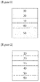
- FIG. 1 is a view illustrating a polarizing plate laminate comprising a first adhesive layer 20 and a first separate film 30 which are provided on one surface of a polarizing plate 10, and a second adhesive layer 40 and a second separate film 50 which are provided on the other surface of the polarizing plate 10.
- the second separate film 50 has a total thickness of more than 75 ⁇ m and 150 ⁇ m or less.
- FIG. 2 is a view illustrating a polarizing plate laminate in which the second separate film 50 has a double-layered structure.
- a region where the second separate film is provided can be a region where the liquid crystal panel or optical film of the liquid crystal display device is disposed. That is, a liquid crystal display device manufactured using the polarizing plate laminate according to an exemplary embodiment of the present application can be manufactured by removing the second separate film of the polarizing plate laminate and attaching a liquid crystal panel or optical film to a surface from which the second separate film of the polarizing plate laminate is removed.
- a general polarizing plate structure in the related art is schematically illustrated in the following FIG. 4 .
- the polarizing plate in the related art comprises a polarizing plate 10, a protective film 60 provided on one surface of the polarizing plate 10, and a separate film 70 provided on the other surface of the polarizing plate 10.
- a protective film 60 of a polarizing plate in the related art has a thickness of about 50 ⁇ m to 60 ⁇ m, and the protective film 60 served to stably control the curl of the polarizing plate.
- the polarizing plate laminate according to an exemplary embodiment of the present application is a polarizing plate laminate in which in order to suppress a phenomenon in which air bubbles can be generated on a bonding surface of a liquid crystal panel or optical film of a liquid crystal display device and a polarizing plate during a process of attaching the liquid crystal panel or optical film of the liquid crystal display device to the polarizing plate, the thickness of a second separate film provided on a side opposite to the bonding surface is adjusted to more than 75 ⁇ m and 150 ⁇ m or less, and the polarizing plate laminate according to an exemplary embodiment of the present application is different from a polarizing plate in the related art in terms of structure and object thereof.
- the method for manufacturing a polarizing plate laminate according to an exemplary embodiment of the present application can further comprise: removing the first separate film; and attaching a liquid crystal panel or optical film of a liquid crystal display device to the polarizing plate, such that a surface of the polarizing plate laminate from which the first separate film is removed is bonded to one surface of the liquid crystal panel or optical film.
- the optical film can comprise one or more of an antiglare film, a hard coating film, an anti-reflection film, an Anti-Glare & Low-Reflection (AGLR) film, and the like, and is not limited thereto.
- the optical film can be manufactured by a method known in the art. Further, the optical film can be a polycarbonate film.
- the method for manufacturing a polarizing plate laminate according to an exemplary embodiment of the present application can further comprise removing the second separate film after the attaching of the liquid crystal panel or optical film of the liquid crystal display device to the polarizing plate. After the removing of the second separate film, one or more of a liquid crystal panel, an optical film, and the like known in the art can be further attached, and can be provided on a liquid crystal panel, an optical film, and the like known in the art.
- the polarizing plate can comprise a polarizer and a protective film on at least one surface of the polarizer.
- the polarizer protective film can be a triacetate cellulose (TAC) film, a cycloolefin polymer (COP), an acrylic film, and the like, and is not limited thereto.
- TAC triacetate cellulose
- COP cycloolefin polymer
- acrylic film and the like, and is not limited thereto.
- the polarizer is not particularly limited, and a polarizer well-known in the art, for example, a film composed of polyvinyl alcohol (PVA) comprising iodine or a dichroic dye can be used.
- PVA polyvinyl alcohol
- the polarizer exhibits a characteristic capable of extracting only light oscillating in one direction from light incident while oscillating in various directions. These characteristics can be achieved by stretching an iodine-absorbed polyvinyl alcohol (PVA) under high tension.
- PVA polyvinyl alcohol
- a polarizer can be formed by a step of swelling a PVA film by immersing the PVA film in an aqueous solution, a step of dyeing the swollen PVA film with a dichroic substance imparting a polarization property to the swollen PVA film, a stretching step of arranging the dichroic dye substance in parallel with the stretching direction by stretching the dyed PVA film, and a color correcting step of correcting the color of the PVA film subjected to the stretching step.
- the polarizing plate of the present application is not limited thereto.
- liquid crystal display device manufactured by using the polarizing plate laminate.
- the liquid crystal display device can comprise a configuration known in the art, except for being manufactured by using the polarizing plate laminate according to an exemplary embodiment of the present application.
- the liquid crystal display device can comprise: a liquid crystal panel; a first polarizing plate provided on the viewing side of the liquid crystal panel; a second polarizing plate provided on a side opposite to the viewing side of the liquid crystal panel; and a backlight unit provided on a side opposite to a surface of the second polarizing plate facing the liquid crystal panel.
- the first polarizing plate or second polarizing plate can be a polarizing plate laminate according to an exemplary embodiment of the present application.
- the liquid crystal panel can further comprise a separate polarizing plate instead of the polarizing plate laminate according to an exemplary embodiment of the present application, and in this case, the polarizing plate further comprised can be a polarizing plate known in the art.
- the term "viewing side” means a surface or direction arranged so as to face the viewer side when a polarizing plate is mounted to a display device such as a liquid crystal display device.
- the “side opposite to the viewing side” means a side opposite to the viewer, that is, a surface or direction arranged so as to face a backlight unit when a polarizing plate is mounted on a display device such as a liquid crystal display device.
- the liquid crystal display device can be a liquid crystal display device for a vehicle.
- a first separate film polyethylene terephthalate, PET
- a second separate film polyethylene terephthalate, PET
- the first separate film a single-layered film having a thickness of 38 ⁇ m, manufactured by Mitsubishi Corporation
- the second separate film a single-layered film having a thickness of 93 ⁇ m, manufactured by LG Chem, was used.
- the polycarbonate film was laminated with the polarizing plate (using a lamination facility manufactured by Taechang), such that a surface of the polarizing plate from which the first separate film was removed was bonded to one surface of a polycarbonate film (Shinetech Co.).
- the lamination speed during the lamination process was 400 mm/min.
- a process was performed in the same manner as in Example 1, except that as the second separate film, a double-layered film having a total thickness of 131 ⁇ m was used by laminating a single-layered film (Mitsubishi) having a thickness of 38 ⁇ m with a single-layered film (LG Chem) having a thickness of 93 ⁇ m.
- a process was performed in the same manner as in Example 1, except that as the second separate film, a double-layered film having a total thickness of 143 ⁇ m was used by laminating a single-layered film (Mitsubishi) having a thickness of 50 ⁇ m with a single-layered film (LG Chem) having a thickness of 93 ⁇ m.
- a process was performed in the same manner as in Example 1, except that as the second separate film, a single-layered film (Mitsubishi) having a thickness of 38 ⁇ m was used.
- a process was performed in the same manner as in Example 1, except that as the second separate film, a single-layered film (Mitsubishi) having a thickness of 50 ⁇ m was used.
- a process was performed in the same manner as in Example 1, except that as the second separate film, a single-layered film (Toray) having a thickness of 75 ⁇ m was used.
- a process was performed in the same manner as in Example 1, except that as the second separate film, a double-layered film having a total thickness of 168 ⁇ m was used by laminating a single-layered film (Toray) having a thickness of 75 ⁇ m with a single-layered film (LG Chem) having a thickness of 93 ⁇ m.
- Toray a single-layered film having a thickness of 75 ⁇ m
- LG Chem a single-layered film having a thickness of 93 ⁇ m.
- the polarizing plate laminate according to an exemplary embodiment of the present application can prevent defects such as the sagging phenomenon of a polarizing plate during a process of attaching a liquid crystal panel or optical film of a liquid crystal display device to the polarizing plate by comprising a second separate film having a total thickness of more than 75 ⁇ m and 150 ⁇ m or less.
Landscapes
- Physics & Mathematics (AREA)
- Optics & Photonics (AREA)
- General Physics & Mathematics (AREA)
- Nonlinear Science (AREA)
- Crystallography & Structural Chemistry (AREA)
- Chemical & Material Sciences (AREA)
- Mathematical Physics (AREA)
- Engineering & Computer Science (AREA)
- Quality & Reliability (AREA)
- Polarising Elements (AREA)
- Liquid Crystal (AREA)
- Surface Treatment Of Optical Elements (AREA)
- Laminated Bodies (AREA)
- Adhesive Tapes (AREA)
Abstract
Description
- This application claims priority to and the benefit of
Korean Patent Application No. 10-2019-0137106 filed in the Korean Intellectual Property Office on October 31, 2019 - The present application relates to a polarizing plate laminate and a method for manufacturing thereof.
- A liquid crystal display device is one of the flat panel displays which have been widely used from mobile phones or portable small electronic devices to large electronic devices such as personal computers or televisions, and whose use is gradually expanding.
- As the use of display devices has expanded, the places where the display devices are placed and their positions have become diversified, but the flat panel display has a problem in that a clear image cannot be obtained when viewed from another direction rather than the front of the display. In particular, a display for a vehicle has a problem in that a clear image cannot be obtained from the driver's visual field because the position of the display and the line of sight of the driver are not parallel.
- Therefore, in order to solve these problems, there is a need for developing a display device capable of improving the viewing angle and the contrast ratio.
- The present application has been made in an effort to provide a polarizing plate laminate and a method for manufacturing thereof.
- An exemplary embodiment of the present application provides a polarizing plate laminate comprising:
- a polarizing plate;
- a first adhesive layer and a first separate film which are provided on one surface of the polarizing plate; and
- a second adhesive layer and a second separate film which are provided on the other surface of the polarizing plate,
- in which the second separate film has a total thickness of more than 75 µm and 150 µm or less.
- Further, another exemplary embodiment of the present application provides a method for manufacturing a polarizing plate laminate, the method comprising:
- applying a first adhesive layer to one surface of a polarizing plate and applying a second adhesive layer to the other surface thereof; and
- laminating a first separate film on the first adhesive layer and laminating a second separate film on the second adhesive layer,
- in which the second separate film has a total thickness of more than 75 µm and 150 µm or less.
- The polarizing plate laminate according to an exemplary embodiment of the present application can prevent defects such as the sagging phenomenon of a polarizing plate during a process of attaching a liquid crystal panel or optical film of a liquid crystal display device to the polarizing plate by comprising a second separate film having a total thickness of more than 75 µm and 150 µm or less.
- Therefore, it is possible to suppress a phenomenon in which bubbles can be generated on the bonding surface between the liquid crystal panel or optical film of the liquid crystal display device and the polarizing plate during the process of attaching the liquid crystal panel or optical film of the liquid crystal display device to the polarizing plate.
-
-
FIGS. 1 and 2 are views each schematically illustrating a polarizing plate laminate according to an exemplary embodiment of the present application. -
FIG. 3 is a view illustrating the results of attaching the optical film to the polarizing plate according to Example 1 and Comparative Example 1 of the present application. -
FIG. 4 is a view schematically illustrating the structure of a polarizing plate in the related art. -
- 10: Polarizing plate
- 20: First adhesive layer
- 30: First separate film
- 40: Second adhesive layer
- 50: Second separate film
- 60: Protective film
- 70: separate film
- Hereinafter, preferred exemplary embodiments of the present application will be described. However, the exemplary embodiments of the present application can be modified into various other forms, and the scope of the present application is not limited to the exemplary embodiments which will be described below. Further, the exemplary embodiments of the present application are provided to explain the present invention in more detail to a person with ordinary skill in the art.
- Typically, a process of manufacturing a display device comprises a process of attaching a liquid crystal panel or optical film of a liquid crystal display device to a polarizing plate. In a process of attaching a liquid crystal panel or optical film of a liquid crystal display device to a polarizing plate in the related art, there can occur defects such as a polarizing plate sagging phenomenon between a roll operating for the attachment process and a table on which the polarizing plate is placed. Accordingly, in the process of attaching the liquid crystal panel or optical film of the liquid crystal display device to the polarizing plate, a phenomenon in which air bubbles continuously accumulate on the bonding surface can occur, which causes defects to continuously occur, so that there is a problem in that mass production cannot be achieved.
- Thus, the present application is intended to suppress the generation of air bubbles, which can occur due to the sagging of a polarizing plate in a process of attaching a liquid crystal panel or optical film of a liquid crystal display device to the polarizing plate.
- A polarizing plate laminate according to an exemplary embodiment of the present application comprises: a polarizing plate; a first adhesive layer and a first separate film which are provided on one surface of the polarizing plate; and a second adhesive layer and a second separate film which are provided on the other surface of the polarizing plate, in which the second separate film has a total thickness of more than 75 µm and 150 µm or less.
- Further, a method for manufacturing a display device according to an exemplary embodiment of the present application comprises: applying a first adhesive layer to one surface of a polarizing plate and applying a second adhesive layer to the other surface thereof; and laminating a first separate film on the first adhesive layer and laminating a second separate film on the second adhesive layer, wherein the second separate film has a total thickness of more than 75 µm and 150 µm or less.
- In an exemplary embodiment of the present application, the first separate film and the second separate film are films which are temporarily attached to protect the surface of the polarizing plate until the polarizing plate is bonded to the liquid crystal panel or another optical member.
- The first separate film can have a thickness of 10 µm to 75 µm.
- The second separate film can have a single-layered structure or a multi-layered structure. The second separate film can have a total thickness of more than 75 µm and 150 µm or less , 80 µm to 150 µm, and 90 µm to 140 µm. When the second separate film has a total thickness of 75 µm or less, defects such as a sagging phenomenon of a polarizing plate can occur during a process of attaching a liquid crystal panel or optical film of a liquid crystal display device to the polarizing plate, and when the second separate film has a total thickness of more than 150 µm, defects can occur during a process of peeling the second separate film. Accordingly, when the second separate film has a total thickness of more than 75 µm and 150 µm or less, it is possible to effectively prevent defects such as the sagging phenomenon of a polarizing plate during a process of attaching a liquid crystal panel or optical film of a liquid crystal display device to the polarizing plate.
- The second separate film can have a single-layered structure or a double-layered structure. When the second separate film has a double-layered structure, as a second separate film (A) which directly contacts the polarizing plate, it is possible to apply a separate film having no adhesive characteristics on the surface thereof, and as a second separate film (B) which does not directly contact the polarizing plate, it is possible to apply a separate film having adhesive characteristics on a surface attached to the second separate film (A).
- The first separate film and the second separate film can each comprise one or more of a polyethylene-based resin such as polyethylene; a polypropylene-based resin such as polypropylene; a polyester-based resin such as polyethylene terephthalate or polyethylene naphthalate; and a polycarbonate-based resin.
- In an exemplary embodiment of the present application, a first adhesive layer is provided between the polarizing plate and the first separate film, and a second adhesive layer is provided between the polarizing plate and the second separate film. Accordingly, the first separate film can be attached by a first adhesive layer applied on one surface of the polarizing plate, and the second separate film can be attached by a second adhesive layer applied on the other surface of the polarizing plate.
- The first adhesive layer and the second adhesive layer can comprise a general-purpose adhesive, and more specifically, can be composed of an adhesive composition comprising a resin such as a (meth) acrylic resin, a rubber-based resin, a urethane-based resin, an ester-based resin, a silicone-based resin, and a polyvinyl ether-based resin as a main component. Among them, an adhesive composition comprising a (meth) acrylic resin having excellent transparency, weatherability, heat resistance and the like as a base polymer is suitable. The adhesive composition can be an active energy ray-curable type or a thermosetting type.
- In an exemplary embodiment of the present application, the laminating of the first separate film and the second separate film on the polarizing plate to which the first adhesive layer and the second adhesive layer are applied can be performed by a roll to roll process. A process of attaching a first separate film and a second separate film on the polarizing plate can be performed by a lamination process using a lamination roll after preparing the corresponding products wound on each roll.
- A polarizing plate laminate according to an exemplary embodiment of the present application is schematically illustrated in the following
FIGS. 1 and 2 . More specifically, the followingFIG. 1 is a view illustrating a polarizing plate laminate comprising a firstadhesive layer 20 and a firstseparate film 30 which are provided on one surface of a polarizingplate 10, and a secondadhesive layer 40 and a secondseparate film 50 which are provided on the other surface of the polarizingplate 10. In this case, the secondseparate film 50 has a total thickness of more than 75 µm and 150 µm or less. Further, the followingFIG. 2 is a view illustrating a polarizing plate laminate in which the secondseparate film 50 has a double-layered structure. - In an exemplary embodiment of the present application, a region where the second separate film is provided can be a region where the liquid crystal panel or optical film of the liquid crystal display device is disposed. That is, a liquid crystal display device manufactured using the polarizing plate laminate according to an exemplary embodiment of the present application can be manufactured by removing the second separate film of the polarizing plate laminate and attaching a liquid crystal panel or optical film to a surface from which the second separate film of the polarizing plate laminate is removed.
- A general polarizing plate structure in the related art is schematically illustrated in the following
FIG. 4 . As illustrated in the followingFIG. 4 , the polarizing plate in the related art comprises apolarizing plate 10, aprotective film 60 provided on one surface of thepolarizing plate 10, and aseparate film 70 provided on the other surface of thepolarizing plate 10. Aprotective film 60 of a polarizing plate in the related art has a thickness of about 50 µm to 60 µm, and theprotective film 60 served to stably control the curl of the polarizing plate. - However, the polarizing plate laminate according to an exemplary embodiment of the present application is a polarizing plate laminate in which in order to suppress a phenomenon in which air bubbles can be generated on a bonding surface of a liquid crystal panel or optical film of a liquid crystal display device and a polarizing plate during a process of attaching the liquid crystal panel or optical film of the liquid crystal display device to the polarizing plate, the thickness of a second separate film provided on a side opposite to the bonding surface is adjusted to more than 75 µm and 150 µm or less, and the polarizing plate laminate according to an exemplary embodiment of the present application is different from a polarizing plate in the related art in terms of structure and object thereof.
- The method for manufacturing a polarizing plate laminate according to an exemplary embodiment of the present application can further comprise: removing the first separate film; and attaching a liquid crystal panel or optical film of a liquid crystal display device to the polarizing plate, such that a surface of the polarizing plate laminate from which the first separate film is removed is bonded to one surface of the liquid crystal panel or optical film.
- The optical film can comprise one or more of an antiglare film, a hard coating film, an anti-reflection film, an Anti-Glare & Low-Reflection (AGLR) film, and the like, and is not limited thereto. The optical film can be manufactured by a method known in the art. Further, the optical film can be a polycarbonate film.
- The method for manufacturing a polarizing plate laminate according to an exemplary embodiment of the present application can further comprise removing the second separate film after the attaching of the liquid crystal panel or optical film of the liquid crystal display device to the polarizing plate. After the removing of the second separate film, one or more of a liquid crystal panel, an optical film, and the like known in the art can be further attached, and can be provided on a liquid crystal panel, an optical film, and the like known in the art.
- As described above, during a process of attaching a liquid crystal panel or optical film of a liquid crystal display device to a polarizing plate in the related art, stress due to the sagging of the polarizing plate occurs, and air bubbles can be generated when the film bending portion due to suction removal is attached to the liquid crystal panel or optical film. However, according to an exemplary embodiment of the present application, it is possible to prevent defects such as the sagging phenomenon of a polarizing plate during the process of attaching a liquid crystal panel or optical film of a liquid crystal display device to the polarizing plate by using a polarizing plate laminate comprising a second separate film having a total thickness of more than 75 µm and 150 µm or less.
- In an exemplary embodiment of the present application, the polarizing plate can comprise a polarizer and a protective film on at least one surface of the polarizer.
- The polarizer protective film can be a triacetate cellulose (TAC) film, a cycloolefin polymer (COP), an acrylic film, and the like, and is not limited thereto.
- The polarizer is not particularly limited, and a polarizer well-known in the art, for example, a film composed of polyvinyl alcohol (PVA) comprising iodine or a dichroic dye can be used.
- The polarizer exhibits a characteristic capable of extracting only light oscillating in one direction from light incident while oscillating in various directions. These characteristics can be achieved by stretching an iodine-absorbed polyvinyl alcohol (PVA) under high tension. For example, more specifically, a polarizer can be formed by a step of swelling a PVA film by immersing the PVA film in an aqueous solution, a step of dyeing the swollen PVA film with a dichroic substance imparting a polarization property to the swollen PVA film, a stretching step of arranging the dichroic dye substance in parallel with the stretching direction by stretching the dyed PVA film, and a color correcting step of correcting the color of the PVA film subjected to the stretching step. However, the polarizing plate of the present application is not limited thereto.
- Further, another exemplary embodiment of the present application provides a liquid crystal display device manufactured by using the polarizing plate laminate. The liquid crystal display device can comprise a configuration known in the art, except for being manufactured by using the polarizing plate laminate according to an exemplary embodiment of the present application.
- For example, the liquid crystal display device according to an exemplary embodiment of the present application can comprise: a liquid crystal panel; a first polarizing plate provided on the viewing side of the liquid crystal panel; a second polarizing plate provided on a side opposite to the viewing side of the liquid crystal panel; and a backlight unit provided on a side opposite to a surface of the second polarizing plate facing the liquid crystal panel. In this case, the first polarizing plate or second polarizing plate can be a polarizing plate laminate according to an exemplary embodiment of the present application. In addition, the liquid crystal panel can further comprise a separate polarizing plate instead of the polarizing plate laminate according to an exemplary embodiment of the present application, and in this case, the polarizing plate further comprised can be a polarizing plate known in the art.
- In the present application, the term "viewing side" means a surface or direction arranged so as to face the viewer side when a polarizing plate is mounted to a display device such as a liquid crystal display device. In contrast, the "side opposite to the viewing side" means a side opposite to the viewer, that is, a surface or direction arranged so as to face a backlight unit when a polarizing plate is mounted on a display device such as a liquid crystal display device.
- In an exemplary embodiment of the present application, the liquid crystal display device can be a liquid crystal display device for a vehicle.
- Hereinafter, exemplary embodiments described in the present specification will be exemplified through Examples. However, the scope of the exemplary embodiments is not intended to be limited by the following Examples.
- After an adhesive (LG Chem, highly durable adhesive) was applied to both surfaces of a polarizing plate (LG Chem, highly durable polarizing plate), a first separate film (polyethylene terephthalate, PET) was laminated on one surface of the polarizing plate, and a second separate film (polyethylene terephthalate, PET) was laminated on the other surface of the polarizing plate using a roll to roll process. Further, as the first separate film, a single-layered film having a thickness of 38 µm, manufactured by Mitsubishi Corporation, was used, and as the second separate film, a single-layered film having a thickness of 93 µm, manufactured by LG Chem, was used.
- After the first separate film of the polarizing plate was removed, the polycarbonate film was laminated with the polarizing plate (using a lamination facility manufactured by Taechang), such that a surface of the polarizing plate from which the first separate film was removed was bonded to one surface of a polycarbonate film (Shinetech Co.). The lamination speed during the lamination process was 400 mm/min.
- A process was performed in the same manner as in Example 1, except that as the second separate film, a double-layered film having a total thickness of 131 µm was used by laminating a single-layered film (Mitsubishi) having a thickness of 38 µm with a single-layered film (LG Chem) having a thickness of 93 µm.
- A process was performed in the same manner as in Example 1, except that as the second separate film, a double-layered film having a total thickness of 143 µm was used by laminating a single-layered film (Mitsubishi) having a thickness of 50 µm with a single-layered film (LG Chem) having a thickness of 93 µm.
- A process was performed in the same manner as in Example 1, except that as the second separate film, a single-layered film (Mitsubishi) having a thickness of 38 µm was used.
- A process was performed in the same manner as in Example 1, except that as the second separate film, a single-layered film (Mitsubishi) having a thickness of 50 µm was used.
- A process was performed in the same manner as in Example 1, except that as the second separate film, a single-layered film (Toray) having a thickness of 75 µm was used.
- A process was performed in the same manner as in Example 1, except that as the second separate film, a double-layered film having a total thickness of 168 µm was used by laminating a single-layered film (Toray) having a thickness of 75 µm with a single-layered film (LG Chem) having a thickness of 93 µm.
- After the lamination process between the polarizing plate according to the Examples and the Comparative Examples and the polycarbonate film, the presence or absence of defects in the bonding surface between the polarizing plate and the polycarbonate film was evaluated, and the results are shown in the following Table 1. Furthermore, the results of attaching the optical film to the polarizing plate according to Example 1 and Comparative Example 1 are shown in the following
FIG. 3 . The evaluation results in the following Table 1 were evaluated based on the presence or absence of defects such as air bubbles when the bonding surface between the polarizing plate and the polycarbonate film was visually confirmed.[Table 1] Evaluation result Example 1 OK Example 2 OK Example 3 OK Comparative Example 1 Occurrence of defects Comparative Example 2 Occurrence of defects Comparative Example 3 Occurrence of defects Comparative Example 4 Occurrence of defects - As shown in the results of the following
FIG. 3 , when the optical film was attached to the polarizing plate according to Example 1, no air bubbles were generated on the bonding surface between the optical film and the polarizing plate. However, when the optical film was attached to the polarizing plate according to Comparative Example 1, a sagging phenomenon of the polarizing plate occurred during the process of attaching the optical film to the polarizing plate, so that it could be confirmed that air bubbles are generated on the bonding surface between the optical film and the polarizing plate. - Accordingly, the polarizing plate laminate according to an exemplary embodiment of the present application can prevent defects such as the sagging phenomenon of a polarizing plate during a process of attaching a liquid crystal panel or optical film of a liquid crystal display device to the polarizing plate by comprising a second separate film having a total thickness of more than 75 µm and 150 µm or less.
- Therefore, it is possible to suppress a phenomenon in which air bubbles can be generated on the bonding surface between the liquid crystal panel or optical film of the liquid crystal display device and the polarizing plate during the process of attaching the liquid crystal panel or optical film of the liquid crystal display device to the polarizing plate.
Claims (13)
- A polarizing plate laminate comprising:a polarizing plate;a first adhesive layer and a first separate film which are provided on one surface of the polarizing plate; anda second adhesive layer and a second separate film which are provided on the other surface of the polarizing plate,wherein the second separate film has a total thickness of more than 75 µm and 150 µm or less.
- The polarizing plate laminate of claim 1, wherein the second separate film has a single-layered structure or a multi-layered structure.
- The polarizing plate laminate of claim 1, wherein the first separate film has a thickness of 10 µm to 75 µm.
- The polarizing plate laminate of claim 1, wherein the first separate film and the second separate film each comprise one or more of a polyethylene-based resin, a polypropylene-based resin, a polyester-based resin, and a polycarbonate-based resin.
- The polarizing plate laminate of claim 1, wherein a region where the second separate film is provided is a region where the liquid crystal panel or optical film of the liquid crystal display device is disposed.
- A method for manufacturing a polarizing plate laminate, the method comprising:applying a first adhesive layer to one surface of a polarizing plate and applying a second adhesive layer to the other surface thereof; andlaminating a first separate film on the first adhesive layer and laminating a second separate film on the second adhesive layer,wherein the second separate film has a total thickness of more than 75 µm and 150 µm or less.
- The method of claim 6, wherein the second separate film has a single-layered structure or a multi-layered structure.
- The method of claim 6, wherein the first separate film has a thickness of 10 µm to 75 µm.
- The method of claim 6, wherein the first separate film and the second separate film each comprise one or more of a polyethylene-based resin, a polypropylene-based resin, a polyester-based resin, and a polycarbonate-based resin.
- The method of claim 6, wherein the laminating of the first separate film and the second separate film is performed by a roll to roll process.
- The method of claim 6, further comprising: removing the first separate film; and attaching a liquid crystal panel or optical film of a liquid crystal display device to the polarizing plate, such that a surface of the polarizing plate laminate from which the first separate film is removed is bonded to one surface of the liquid crystal panel or optical film.
- The method of claim 11, wherein the optical film comprises one or more of an antiglare film, a hard coating film, an anti-reflection film, and an Anti-Glare & Low-Reflection (AGLR) film.
- The method of claim 11, wherein the optical film is a polycarbonate film.
Applications Claiming Priority (2)
| Application Number | Priority Date | Filing Date | Title |
|---|---|---|---|
| KR20190137106 | 2019-10-31 | ||
| PCT/KR2020/014489 WO2021085933A1 (en) | 2019-10-31 | 2020-10-22 | Polarizing plate laminate and method for preparing same |
Publications (2)
| Publication Number | Publication Date |
|---|---|
| EP4052898A1 true EP4052898A1 (en) | 2022-09-07 |
| EP4052898A4 EP4052898A4 (en) | 2022-11-23 |
Family
ID=75714649
Family Applications (1)
| Application Number | Title | Priority Date | Filing Date |
|---|---|---|---|
| EP20883662.7A Pending EP4052898A4 (en) | 2019-10-31 | 2020-10-22 | Polarizing plate laminate and method for preparing same |
Country Status (7)
| Country | Link |
|---|---|
| US (1) | US12204198B2 (en) |
| EP (1) | EP4052898A4 (en) |
| JP (1) | JP7719727B2 (en) |
| KR (1) | KR102452788B1 (en) |
| CN (1) | CN113853538A (en) |
| TW (1) | TWI792083B (en) |
| WO (1) | WO2021085933A1 (en) |
Families Citing this family (1)
| Publication number | Priority date | Publication date | Assignee | Title |
|---|---|---|---|---|
| CN111286280B (en) * | 2018-12-06 | 2022-06-03 | 深圳光峰科技股份有限公司 | Screen splicing structure and forming method thereof |
Family Cites Families (39)
| Publication number | Priority date | Publication date | Assignee | Title |
|---|---|---|---|---|
| JPH1044284A (en) | 1996-08-08 | 1998-02-17 | Mitsubishi Plastics Ind Ltd | Glass reinforcement film |
| JP2001108826A (en) * | 1999-10-04 | 2001-04-20 | Sekisui Chem Co Ltd | Polarizer protective film, method for producing the same, and polarizing plate |
| JP3713183B2 (en) | 2000-04-26 | 2005-11-02 | リンテック株式会社 | Peeling sheet with polarizing plate, production method thereof, peeling method of polarizing plate, and peeling device therefor |
| TWI251089B (en) | 2000-06-19 | 2006-03-11 | Nitto Denko Corp | Polarizer, polarizing plate, and liquid crystal display using the same |
| JP2005283846A (en) | 2004-03-29 | 2005-10-13 | Nitto Denko Corp | Optical film and liquid crystal display device |
| JP5030134B2 (en) | 2005-08-18 | 2012-09-19 | 株式会社リコー | Polarization conversion element, polarization conversion optical system, and image projection apparatus |
| JP4861944B2 (en) * | 2007-09-21 | 2012-01-25 | 富士フイルム株式会社 | Optical compensation film manufacturing method, optical compensation film, polarizing plate, and liquid crystal display device |
| JP4603572B2 (en) | 2007-11-14 | 2010-12-22 | 日東電工株式会社 | Adhesive for polarizing plate, polarizing plate, method for producing the same, optical film, and image display device |
| KR20090101763A (en) | 2008-03-24 | 2009-09-29 | 동우 화인켐 주식회사 | Ligth control ultra thin polarizing plate and liquid crystal display device |
| KR101210985B1 (en) | 2008-12-26 | 2012-12-11 | 주식회사 엘지화학 | Lenticular optical film with reduced moire and backlight unit comprising the same |
| JP4428470B1 (en) * | 2009-06-08 | 2010-03-10 | 東洋インキ製造株式会社 | Polarizing plate and adhesive composition for forming polarizing plate |
| KR20110002676A (en) * | 2009-07-02 | 2011-01-10 | 웅진케미칼 주식회사 | Integrated high-brightness polarizing sheet, liquid crystal display panel rear polarizing film applying the same, and liquid crystal display having the same |
| KR101442667B1 (en) | 2011-02-10 | 2014-09-19 | 주식회사 엘지화학 | Polarizer, manufacturing method for the same and display device employing thereof |
| JP2013008019A (en) * | 2011-05-26 | 2013-01-10 | Nitto Denko Corp | Polarization film having adhesive layer and image display unit |
| KR101411020B1 (en) | 2011-12-29 | 2014-06-24 | 제일모직주식회사 | Adhesive for polarizer plate, polarizer plate comprising adhesive layer including the same and liquid crystal display comprising the same |
| JP5909454B2 (en) | 2012-03-30 | 2016-04-26 | 富士フイルム株式会社 | Anti-glare film, method for producing the same, polarizing plate, and image display device |
| JP6275945B2 (en) * | 2012-12-10 | 2018-02-07 | 日東電工株式会社 | Optical film with double-sided pressure-sensitive adhesive, and method for manufacturing an image display device using the same |
| JP2014122984A (en) | 2012-12-20 | 2014-07-03 | Dainippon Printing Co Ltd | Manufacturing method of optical film, optical film, and image display unit |
| JP2014126598A (en) * | 2012-12-25 | 2014-07-07 | Sumitomo Chemical Co Ltd | Anti-glare film and anti-glare polarizing plate |
| KR20150050063A (en) * | 2013-10-31 | 2015-05-08 | 제일모직주식회사 | Depolarization film and display device including the same |
| TWI628457B (en) | 2014-04-17 | 2018-07-01 | 日商大日本印刷股份有限公司 | Anti-glare film, polarizing plate, liquid crystal panel, and image display device |
| KR101882560B1 (en) | 2014-08-01 | 2018-07-26 | 삼성에스디아이 주식회사 | Adhesive composition, adhesive film, optical member and adhesive sheet |
| JP6826886B2 (en) | 2014-09-09 | 2021-02-10 | 住友化学株式会社 | Method for manufacturing polarizing plate and liquid crystal panel |
| JP6580315B2 (en) * | 2014-10-15 | 2019-09-25 | 日東電工株式会社 | Optical film with double-sided pressure-sensitive adhesive, method for producing image display device using the same, and curl suppression method for optical film with double-sided pressure-sensitive adhesive |
| JP2016118771A (en) | 2014-12-18 | 2016-06-30 | 住友化学株式会社 | Polarizing plate with protective film and laminate including the same |
| CN105717569A (en) * | 2014-12-18 | 2016-06-29 | 住友化学株式会社 | Polarizing plate with protection film and laminated body comprising same |
| JP6258911B2 (en) * | 2014-12-22 | 2018-01-10 | 住友化学株式会社 | Polarizing plate with protective film and laminate including the same |
| CN105717572B (en) * | 2014-12-22 | 2020-05-12 | 住友化学株式会社 | Polarizing plate with protective film and laminate containing the same |
| JP6782071B2 (en) | 2015-01-20 | 2020-11-11 | 日東電工株式会社 | Polarizing film with double-sided adhesive layer, its manufacturing method and image display device |
| CN105807356B (en) * | 2015-01-20 | 2020-10-02 | 日东电工株式会社 | Polarizing film with adhesive layers on both sides, method for producing the same, and image display device |
| JP6095711B2 (en) | 2015-02-19 | 2017-03-15 | 住友化学株式会社 | Method for producing laminated optical film |
| JP6532767B2 (en) | 2015-06-16 | 2019-06-19 | 住友化学株式会社 | Manufacturing method of bonding optical film |
| CN106324741A (en) * | 2015-06-30 | 2017-01-11 | 住友化学株式会社 | Polarizing plate, liquid crystal panel and liquid crystal display device |
| KR102805185B1 (en) | 2015-10-02 | 2025-05-08 | 스미또모 가가꾸 가부시키가이샤 | Method for manufacturing polarizing plate, liquid crystal panel and protective film attached thereto |
| JP2017111361A (en) | 2015-12-18 | 2017-06-22 | 住友化学株式会社 | Manufacturing method of single-sided protective polarizing plate |
| KR101886576B1 (en) * | 2016-07-20 | 2018-08-07 | 스미또모 가가꾸 가부시키가이샤 | Separator film layered adhesive layer-containing optical film |
| JP2018022135A (en) | 2016-07-20 | 2018-02-08 | 住友化学株式会社 | Separator film laminated optical film with adhesive layer |
| KR20190137106A (en) | 2017-04-28 | 2019-12-10 | 닛뽄 가야쿠 가부시키가이샤 | Maleimide resin composition, prepreg and cured product thereof |
| KR102244789B1 (en) | 2017-12-15 | 2021-04-26 | 주식회사 엘지화학 | Polarzing plate, polarizing plate-carrier film laminate, the method for manufacturing the polarizing plate and the active energy beam-cured composition for protective layer of polarizer |
-
2020
- 2020-10-22 WO PCT/KR2020/014489 patent/WO2021085933A1/en not_active Ceased
- 2020-10-22 JP JP2021567876A patent/JP7719727B2/en active Active
- 2020-10-22 KR KR1020200137603A patent/KR102452788B1/en active Active
- 2020-10-22 CN CN202080036361.5A patent/CN113853538A/en active Pending
- 2020-10-22 US US17/609,635 patent/US12204198B2/en active Active
- 2020-10-22 EP EP20883662.7A patent/EP4052898A4/en active Pending
- 2020-10-29 TW TW109137525A patent/TWI792083B/en active
Also Published As
| Publication number | Publication date |
|---|---|
| EP4052898A4 (en) | 2022-11-23 |
| KR20210052267A (en) | 2021-05-10 |
| CN113853538A (en) | 2021-12-28 |
| TW202134700A (en) | 2021-09-16 |
| US12204198B2 (en) | 2025-01-21 |
| US20220229330A1 (en) | 2022-07-21 |
| JP2022532722A (en) | 2022-07-19 |
| KR102452788B1 (en) | 2022-10-11 |
| TWI792083B (en) | 2023-02-11 |
| WO2021085933A1 (en) | 2021-05-06 |
| JP7719727B2 (en) | 2025-08-06 |
Similar Documents
| Publication | Publication Date | Title |
|---|---|---|
| CN103389535B (en) | Method for manufacturing polarizing film, polarizing film, polarizing plate and image display device | |
| US9164210B2 (en) | Optical laminated body, optical laminated body set, and liquid crystal panel using optical laminated body or optical laminated body set | |
| CN110730717B (en) | Optical film, peeling method, and method for manufacturing optical display panel | |
| JP6926199B2 (en) | A polarizing plate, an image display device, and a method for manufacturing the image display device. | |
| KR102593490B1 (en) | Polarizer and method of manufacturing polarizer | |
| KR20120025428A (en) | Polarizing film, optical film laminate including polarizing film, stretched laminate for use in production of optical film laminate including polarizing film, production methods for them, and organic el display device having polarizing film | |
| KR20090084709A (en) | Manufacturing method of polarizing plate | |
| CN108885298A (en) | The manufacturing method of optical thin film, stripping means and optical display panel | |
| JP7693324B2 (en) | Optical laminate with pressure-sensitive adhesive layer, image display device, and manufacturing method thereof | |
| US12204198B2 (en) | Polarizing plate laminate and method for preparing same | |
| CN104157222B (en) | Surface protection panel and liquid crystal image display device | |
| KR102940031B1 (en) | Optical laminate having an adhesive layer and an image display device, and a method for manufacturing the same | |
| JP2012048181A (en) | Polarizer and liquid crystal display device using the same | |
| CN106353846A (en) | Manufacturing method of polarizing plate | |
| US20240310563A1 (en) | View blind check film, image display apparatus, and view blind check method | |
| KR20230053310A (en) | Backplate film for oled |
Legal Events
| Date | Code | Title | Description |
|---|---|---|---|
| STAA | Information on the status of an ep patent application or granted ep patent |
Free format text: STATUS: THE INTERNATIONAL PUBLICATION HAS BEEN MADE |
|
| PUAI | Public reference made under article 153(3) epc to a published international application that has entered the european phase |
Free format text: ORIGINAL CODE: 0009012 |
|
| STAA | Information on the status of an ep patent application or granted ep patent |
Free format text: STATUS: REQUEST FOR EXAMINATION WAS MADE |
|
| 17P | Request for examination filed |
Effective date: 20211108 |
|
| AK | Designated contracting states |
Kind code of ref document: A1 Designated state(s): AL AT BE BG CH CY CZ DE DK EE ES FI FR GB GR HR HU IE IS IT LI LT LU LV MC MK MT NL NO PL PT RO RS SE SI SK SM TR |
|
| REG | Reference to a national code |
Ref country code: DE Ref legal event code: R079 Free format text: PREVIOUS MAIN CLASS: B32B0007060000 Ipc: B32B0007023000 |
|
| A4 | Supplementary search report drawn up and despatched |
Effective date: 20221025 |
|
| RIC1 | Information provided on ipc code assigned before grant |
Ipc: G02B 1/04 20060101ALI20221019BHEP Ipc: G02B 5/30 20060101ALI20221019BHEP Ipc: B32B 27/36 20060101ALI20221019BHEP Ipc: B32B 27/08 20060101ALI20221019BHEP Ipc: B32B 7/12 20060101ALI20221019BHEP Ipc: B32B 7/06 20190101ALI20221019BHEP Ipc: B32B 7/023 20190101AFI20221019BHEP |
|
| DAV | Request for validation of the european patent (deleted) | ||
| DAX | Request for extension of the european patent (deleted) | ||
| STAA | Information on the status of an ep patent application or granted ep patent |
Free format text: STATUS: EXAMINATION IS IN PROGRESS |
|
| 17Q | First examination report despatched |
Effective date: 20241204 |
|
| RAP1 | Party data changed (applicant data changed or rights of an application transferred) |
Owner name: SHANJIN OPTOELECTRONICS (SUZHOU) CO., LTD. |