EP4050407B1 - Display device - Google Patents
Display device Download PDFInfo
- Publication number
- EP4050407B1 EP4050407B1 EP19949736.3A EP19949736A EP4050407B1 EP 4050407 B1 EP4050407 B1 EP 4050407B1 EP 19949736 A EP19949736 A EP 19949736A EP 4050407 B1 EP4050407 B1 EP 4050407B1
- Authority
- EP
- European Patent Office
- Prior art keywords
- bar
- base
- frame
- support
- slot
- Prior art date
- Legal status (The legal status is an assumption and is not a legal conclusion. Google has not performed a legal analysis and makes no representation as to the accuracy of the status listed.)
- Active
Links
Images






Classifications
-
- G—PHYSICS
- G02—OPTICS
- G02F—OPTICAL DEVICES OR ARRANGEMENTS FOR THE CONTROL OF LIGHT BY MODIFICATION OF THE OPTICAL PROPERTIES OF THE MEDIA OF THE ELEMENTS INVOLVED THEREIN; NON-LINEAR OPTICS; FREQUENCY-CHANGING OF LIGHT; OPTICAL LOGIC ELEMENTS; OPTICAL ANALOGUE/DIGITAL CONVERTERS
- G02F1/00—Devices or arrangements for the control of the intensity, colour, phase, polarisation or direction of light arriving from an independent light source, e.g. switching, gating or modulating; Non-linear optics
- G02F1/01—Devices or arrangements for the control of the intensity, colour, phase, polarisation or direction of light arriving from an independent light source, e.g. switching, gating or modulating; Non-linear optics for the control of the intensity, phase, polarisation or colour
- G02F1/13—Devices or arrangements for the control of the intensity, colour, phase, polarisation or direction of light arriving from an independent light source, e.g. switching, gating or modulating; Non-linear optics for the control of the intensity, phase, polarisation or colour based on liquid crystals, e.g. single liquid crystal display cells
- G02F1/133—Constructional arrangements; Operation of liquid crystal cells; Circuit arrangements
- G02F1/1333—Constructional arrangements; Manufacturing methods
- G02F1/1335—Structural association of cells with optical devices, e.g. polarisers or reflectors
- G02F1/1336—Illuminating devices
- G02F1/133602—Direct backlight
- G02F1/133608—Direct backlight including particular frames or supporting means
-
- G—PHYSICS
- G02—OPTICS
- G02F—OPTICAL DEVICES OR ARRANGEMENTS FOR THE CONTROL OF LIGHT BY MODIFICATION OF THE OPTICAL PROPERTIES OF THE MEDIA OF THE ELEMENTS INVOLVED THEREIN; NON-LINEAR OPTICS; FREQUENCY-CHANGING OF LIGHT; OPTICAL LOGIC ELEMENTS; OPTICAL ANALOGUE/DIGITAL CONVERTERS
- G02F1/00—Devices or arrangements for the control of the intensity, colour, phase, polarisation or direction of light arriving from an independent light source, e.g. switching, gating or modulating; Non-linear optics
- G02F1/01—Devices or arrangements for the control of the intensity, colour, phase, polarisation or direction of light arriving from an independent light source, e.g. switching, gating or modulating; Non-linear optics for the control of the intensity, phase, polarisation or colour
- G02F1/13—Devices or arrangements for the control of the intensity, colour, phase, polarisation or direction of light arriving from an independent light source, e.g. switching, gating or modulating; Non-linear optics for the control of the intensity, phase, polarisation or colour based on liquid crystals, e.g. single liquid crystal display cells
- G02F1/133—Constructional arrangements; Operation of liquid crystal cells; Circuit arrangements
- G02F1/1333—Constructional arrangements; Manufacturing methods
- G02F1/1335—Structural association of cells with optical devices, e.g. polarisers or reflectors
- G02F1/1336—Illuminating devices
- G02F1/133602—Direct backlight
- G02F1/133603—Direct backlight with LEDs
-
- G—PHYSICS
- G02—OPTICS
- G02F—OPTICAL DEVICES OR ARRANGEMENTS FOR THE CONTROL OF LIGHT BY MODIFICATION OF THE OPTICAL PROPERTIES OF THE MEDIA OF THE ELEMENTS INVOLVED THEREIN; NON-LINEAR OPTICS; FREQUENCY-CHANGING OF LIGHT; OPTICAL LOGIC ELEMENTS; OPTICAL ANALOGUE/DIGITAL CONVERTERS
- G02F1/00—Devices or arrangements for the control of the intensity, colour, phase, polarisation or direction of light arriving from an independent light source, e.g. switching, gating or modulating; Non-linear optics
- G02F1/01—Devices or arrangements for the control of the intensity, colour, phase, polarisation or direction of light arriving from an independent light source, e.g. switching, gating or modulating; Non-linear optics for the control of the intensity, phase, polarisation or colour
- G02F1/13—Devices or arrangements for the control of the intensity, colour, phase, polarisation or direction of light arriving from an independent light source, e.g. switching, gating or modulating; Non-linear optics for the control of the intensity, phase, polarisation or colour based on liquid crystals, e.g. single liquid crystal display cells
- G02F1/133—Constructional arrangements; Operation of liquid crystal cells; Circuit arrangements
- G02F1/1333—Constructional arrangements; Manufacturing methods
- G02F1/1335—Structural association of cells with optical devices, e.g. polarisers or reflectors
- G02F1/1336—Illuminating devices
- G02F1/133602—Direct backlight
- G02F1/133605—Direct backlight including specially adapted reflectors
-
- G—PHYSICS
- G02—OPTICS
- G02F—OPTICAL DEVICES OR ARRANGEMENTS FOR THE CONTROL OF LIGHT BY MODIFICATION OF THE OPTICAL PROPERTIES OF THE MEDIA OF THE ELEMENTS INVOLVED THEREIN; NON-LINEAR OPTICS; FREQUENCY-CHANGING OF LIGHT; OPTICAL LOGIC ELEMENTS; OPTICAL ANALOGUE/DIGITAL CONVERTERS
- G02F1/00—Devices or arrangements for the control of the intensity, colour, phase, polarisation or direction of light arriving from an independent light source, e.g. switching, gating or modulating; Non-linear optics
- G02F1/01—Devices or arrangements for the control of the intensity, colour, phase, polarisation or direction of light arriving from an independent light source, e.g. switching, gating or modulating; Non-linear optics for the control of the intensity, phase, polarisation or colour
- G02F1/13—Devices or arrangements for the control of the intensity, colour, phase, polarisation or direction of light arriving from an independent light source, e.g. switching, gating or modulating; Non-linear optics for the control of the intensity, phase, polarisation or colour based on liquid crystals, e.g. single liquid crystal display cells
- G02F1/133—Constructional arrangements; Operation of liquid crystal cells; Circuit arrangements
- G02F1/1333—Constructional arrangements; Manufacturing methods
- G02F1/1335—Structural association of cells with optical devices, e.g. polarisers or reflectors
- G02F1/1336—Illuminating devices
- G02F1/133602—Direct backlight
- G02F1/133606—Direct backlight including a specially adapted diffusing, scattering or light controlling members
Definitions
- the present invention relates to a display device.
- a liquid crystal panel of the LCD includes a liquid crystal layer and a TFT substrate and a color filter substrate opposite each other while the liquid crystal layer is interposed therebetween, and may display an image using light provided by a backlight unit.
- a display device includes a display panel, a frame located at the rear of the display panel, a light source located between the display panel and the frame, the light source being configured to provide light to the display panel, an optical layer located between the display panel and the light source, the optical layer being configured to transmit the light provided by the light source, and a support located between the frame and the optical layer, the support being mounted at the frame, the support being configured to support the optical layer, wherein the support includes a base extending long, the base being placed on the frame, a bridge extending from one end to the other end of the base, the bridge being spaced apart from the base at the upper side of the base, a tower extending from the bridge toward the optical layer, a shaft extending from the lower surface of the base toward the frame, and a bar extending long from the shaft in a direction intersecting the longitudinal direction of the base.
- the frame includes a flat portion and an inclined portion extending from the flat portion toward the display panel in the state of being inclined, and the flat portion includes a fixing recess portion recessed from the rear surface of the flat portion toward the front surface of the flat portion and a bar slot formed in the fixing recess portion, the bar slot being cut out such that the bar of the support passes through the bar slot, the bar slot intersecting the longitudinal direction of the base and the longitudinal direction of the bar.
- the support further includes a stopper formed at the outer circumferential surface of the shaft, the stopper being located between the base and the bar, and the frame further includes a stopper slot formed in the fixing recess portion, the stopper slot extending long in a direction intersecting the bar slot, the stopper slot being shorter than the length of the bar slot, the stopper slot corresponding to the stopper.
- the intersection angle formed by the base and the bar may be about 21 degrees.
- the intersection angle formed by the base and the bar slot may be about 14 degrees.
- intersection angle formed by the bar and the bar slot may be about 35 degrees.
- the intersection angle formed by the stopper slot and the bar slot may be about 35 degrees.
- the support is placed in the fixing recess portion, and, when the bar of the support is inserted into the bar slot and is then rotated, the stopper of the support contacts the stopper slot.
- the frame may include a first protrusion hole formed so as to be spaced apart from one end of the stopper slot in the longitudinal direction of the stopper slot and a second protrusion hole formed so as to be spaced apart from the other end of the stopper slot in the longitudinal direction of the stopper slot
- the support may include a first protrusion located adjacent to one end of the bar, the first protrusion protruding from the bar toward the base so as to be inserted into the first protrusion hole, and a second protrusion located adjacent to the other end of the bar, the second protrusion protruding from the bar toward the base so as to be inserted into the second protrusion hole.
- the support may further include a bottom configured to form a step at the lower surface of the base together with the lower surface of the base, and the bottom may be supported at the front surface of the flat portion by the fixing recess portion.
- the display device may further include a reflection sheet located on the frame, the reflection sheet being configured to reflect the light provided by the light source toward the display panel, wherein a portion of the reflection sheet may be inserted into a gap formed between the front surface of the frame and the lower surface of the base by the bottom, and the base of the support may push the upper surface of the reflection sheet.
- a display device has the following effects.
- suffixes such as “module” and “unit” may be used to refer to elements or components. Use of such suffixes herein is merely intended to facilitate description of the specification, and the suffixes do not have any special meaning or function.
- that which is well known to one of ordinary skill in the relevant art has generally been omitted for the sake of brevity.
- the accompanying drawings are used to assist in easy understanding of various technical features and it should be understood that the embodiments presented herein are not limited by the accompanying drawings. As such, the present disclosure should be construed to extend to any alterations, equivalents and substitutes in addition to those which are particularly set out in the accompanying drawings.
- the first short side area SS1 may be referred to as a first side area
- the second short side area SS2 may be referred to as a second side area
- the first long side area LS1 may be referred to as a third side area adjacent to the first side area and the second side area and located between the first side area and the second side area
- the second long side area LS2 may be referred to as a fourth side area adjacent to the first side area and the second side area, located between the first side area and the second side area, and opposite the third side area.
- a first direction DR1 may be a direction parallel to the long sides LS1 and LS2 of the display device 100
- a second direction DR2 may be a direction parallel to the short sides SS1 and SS2 of the display device 100
- a third direction DR3 may be a direction perpendicular to the first direction DR1 and/or the second direction DR2.
- the first direction DR1 and the second direction DR2 may be collectively referred to as a horizontal direction.
- the third direction DR3 may be referred to as a vertical direction.
- the side of the display device 100 at which an image is displayed may be referred to as a front or a front surface.
- the side of the display device 100 at which an image is not observed when the display device 100 displays the image may be referred to as a rear or a rear surface.
- the first long side portion LS1 may be referred to as an upper side or an upper surface
- the second long side portion LS2 may be referred to as a lower side or a lower surface.
- the first short side portion SS1 may be referred to as a right side or a right surface
- the second short side portion SS2 may be referred to as a left side or a left surface.
- the first long side LS1, the second long side LS2, the first short side SS1, and the second short side SS2 may be referred to as edges of the display device 100.
- the points at which the first long side LS1, the second long side LS2, the first short side SS1, and the second short side SS2 join may be referred to as corners.
- the point at which the first long side LS1 and the first short side SS1 join may be referred to as a first corner C1
- the point at which the first long side LS1 and the second short side SS2 join may be referred to as a second corner C2
- the point at which the second short side SS2 and the second long side LS2 join may be referred to as a third corner C3
- the point at which the second long side LS2 and the first short side SS1 join may be referred to as a first corner C4.
- a direction from the first short side SS1 to the second short side SS2 or a direction from the second short side SS2 to the first short side SS1 may be referred to as a leftward-rightward direction LR.
- a direction from the first long side LS1 to the second long side LS2 or a direction from the second long side LS2 to the first long side LS1 may be referred to as an upward-downward direction UD.
- a display panel 110 may located at the front of the display device 100, and may display an image.
- the display panel 110 may have a plurality of pixels, and may set hue, brightness, and saturation per pixel to output an image.
- the display panel 110 may be divided into an active area in which an image is displayed and an inactive area in which no image is displayed.
- the display panel 110 may include a front substrate and a rear substrate opposite each other in the state in which a liquid crystal layer is interposed therebetween.
- the front substrate may include a plurality of pixels, each of which consists of red (R), green (G), and blue (B) subpixels.
- the front substrate may generate a color corresponding to red, green, or blue according to a control signal.
- a front cover 105 may cover at least a portion of the front surface and the side surface of the display panel 110.
- the front cover 105 may have a hollow quadrangular frame shape.
- the frame 130 may support components of the display device 100.
- the backlight unit 120 may be coupled to the frame 130.
- the frame 130 may be made of a metal material, such as an aluminum alloy.
- the reflection sheet 126 may include at least one of a metal or a metal oxide as a reflective material.
- the reflection sheet 126 may include a metal or metal oxide that exhibits high reflectance, such as at least one of aluminum (Al), silver (Ag), gold (Au), or titanium dioxide (TiO 2 ).
- the optical sheet 125 may be located in front of the diffusion plate 129.
- the rear surface of the optical sheet 125 may face the diffusion plate 129, and the front surface of the optical sheet 125 may face the rear surface of the display panel 110.
- the optical sheet 125 may include at least one sheet. Specifically, the optical sheet 125 may include at least one prism sheet and/or at least one diffusion sheet. The plurality of sheets included in the optical sheet 125 may be in an adhered and/or tight contact state.
- the optical sheet 125 may consist of a plurality of sheets having different functions.
- the optical sheet 125 may include first to third optical sheets 125a to 125c.
- the first optical sheet 125a may have the function of a diffusion sheet
- each of the second and third optical sheets 125b and 125c may have the function of a prism sheet.
- the number and/or positions of the diffusion sheets and the prism sheets may be changed.
- a substrate 122 consisting of a plurality of straps extending in the first direction and spaced apart from each other by a predetermined distance in the second direction, which is perpendicular to the first direction, may be provided on the frame 130.
- One side of each of the plurality of substrates 122 may be connected to a wiring electrode 232.
- the wiring electrode 232 may extend in the second direction.
- the wiring electrode 232 may be connected to one side of the substrate 122 in the state of being spaced apart therefrom in the second direction.
- a wiring hole 234 may be formed in one side of the wiring electrode 232.
- the wiring hole 234 may be a micro-hole formed through the frame 130.
- the wiring electrode 232 may extend to the rear surface of the frame 130 through the wiring hole 234.
- the wiring electrode 232 may be electrically connected to an adaptor (not shown) located at the rear surface of the frame 130 through the wiring hole 234.
- the light assemblies 124 may be disposed on the substrate 122 at predetermined intervals in the first direction.
- the diameter of each light assembly 124 may be greater than the width of the substrate 122 in the second direction.
- the frame 130 includes a flat portion 132 and an inclined portion 133.
- the flat portion 132 may be planar.
- the inclined portion 133 extends forwards from the flat portion 132 while having a predetermined inclination relative to the flat portion 132.
- the frame 130 may generally have the shape of a tub.
- the reflection sheet 126 may generally have the shape of a tub so as to correspond to the shape of the frame 130.
- a space may be formed between the inclined portion 133 and the reflection sheet 126.
- the substrate 122 may be mounted or disposed on the flat portion 132.
- a plurality of substrates 122 may be sequentially disposed.
- the plurality of substrates 122 may be spaced apart from each other.
- a first frame 122A may extend long in the leftward-rightward direction LR of the frame 130, and may be disposed in the longitudinal direction of the frame 130.
- a second frame 122B may extend long in the leftward-rightward direction LR of the frame 130, and may be mounted on the frame 130 in the state of being spaced apart from the first frame 122A.
- a third frame 122C may extend long in the leftward-rightward direction LR of the frame 130, and may be mounted on the frame 130 in the state of being spaced apart from the second frame 122B.
- the distance between the substrates 122 may be changed depending on the number of pixels of the display panel 110 (see FIG. 2 ). For example, the distance between the substrates 122 necessary to provide light to a display panel 111 that realizes 8K quality may be less than the distance between the substrates 122 necessary to provide light to a display panel 111 that realizes 4K quality. In the case in which the number of pixels of the display panel 110 is increased or image quality that can be realized by the display panel 110 is increased, the light transmission ratio of the display panel 110 may be reduced. To this end, a large number of substrates 122 may be disposed in order to increase the luminance of light provided by the backlight unit 120 (see FIG. 3 ).
- the reflection sheet 126 may include a plurality of through-holes 235.
- the plurality of through-holes 235 may correspond in number to the plurality of light assemblies 124.
- the reflection sheet 126 may be placed on the frame 130 and/or the substrates 122. At this time, lenses 124b of the plurality of light assemblies 124 may be inserted into the plurality of through-holes 235 so as to protrude above the reflection sheet 126.
- the reflection sheet 126 may be coupled or fixed to the frame 130 via a fixing member 202.
- the support 200 may be mounted on the reflection sheet 126.
- Coupling ribs 130H and 130V may be formed on the upper end of the inclined portion 133 of the frame 130, and the reflection sheet 126 may have coupling holes VH and HH, whereby the coupling ribs 130H and 130V may be inserted into the coupling holes VH and HH. Consequently, the reflection sheet 126 may be fixed to the frame 130.
- the guide panel 117 may be located at the contour of the reflection sheet 126, and may be coupled to the frame 130.
- the guide panel 117 may support the display panel 110 (see FIG. 2 ).
- Guide panels 117 may be located at four sides of the reflection sheet 126.
- the wiring electrode 232 extending from the front surface of the frame 130 through the wiring hole 234 may be electrically connected to a power supply 315.
- the power supply 315 may be a printed circuit board for supplying power to the display device 100.
- the power supply 315 may convert AC power into DC power.
- the power supply 315 may supply current to the light assembly 124 through the wiring electrode 232.
- the power supply 315 may be electrically connected to a main board 321 via the wiring electrode 232.
- the main board 321 may be spaced apart from the power supply 315 by a predetermined distance.
- the main board 321 may be a printed circuit board that provides an interface necessary to operate the display device 100. In addition, the main board 321 may inspect and maintain the operation state of each component of the display device 100.
- the main board 321 and the power supply 315 may be electrically connected to a t-con board 319 via the wiring electrode 232.
- the t-con board 319 may be a printed circuit board for transmitting power or a signal input from the main board 321 or the power supply 315 to the display panel 110.
- the t-con board 319 may be electrically connected to the display panel 110 at the front surface of the frame 130 via a flexible flat cable (FFC) 251.
- FFC flexible flat cable
- the printed circuit boards are shown as being connected to each other. However, the present disclosure is not limited thereto, and only some of the printed circuit boards may be connected to each other.
- the support 200 includes a base 211, a bridge 213, a tower 215, may include a bottom 216, and includes a fixing bar 217.
- the base 211 may be a plate extending long.
- the bridge 213 is spaced apart from the base 211, extends from one end to the other end of the base 211, and may connect the one end to the other end of the base 211.
- the bridge 213 may include a first shoulder 2131, a second shoulder 2132, and a loop 2133.
- the first shoulder 2131 may extend to the upper side of the base 211 while forming an arch at one end of the base 211.
- the second shoulder 2132 may extend to the upper side of the base 211 while forming an arch at the other end of the base 211.
- the loop 2133 may connect the first shoulder 2131 and the second shoulder 2132 to each other.
- the distance between the first shoulder 2131 and the base 211 and/or the distance between the second shoulder 2132 and the base 211 may be greater than the distance between the loop 2133 and the base 211. That is, the upper end surface of the first shoulder 2131 and/or the upper end surface of the second shoulder 2132 may protrude further forwards than the upper surface of the loop 2133.
- the first shoulder 2131, the second shoulder 2132, and/or the loop 2133 may be elastic.
- the fixing slot 134S may be formed by punching the fixing recess portion 134.
- the fixing slot 134S may include bar slots 1341 and 1342, a shaft hole 1343, and a stopper slot 1344.
- the fixing recess portion 134 may have a long axis FL of the frame 130 in the longitudinal direction thereof.
- the base 211 of the support 200 may generally have a rectangular shape.
- the base 211 may have a long side and a short side.
- the long side of the base 211 may be defined as a longitudinal direction
- the short side of the base 211 may be defined as a lateral direction.
- the width D2 of the base 211 or the width D2 of the fixing recess portion 134 may be less than the distance D1 between the substrates 122.
- the longitudinal direction of the base 211 may be parallel to the longitudinal direction of the substrates 122.
Landscapes
- Physics & Mathematics (AREA)
- Nonlinear Science (AREA)
- Mathematical Physics (AREA)
- Chemical & Material Sciences (AREA)
- Crystallography & Structural Chemistry (AREA)
- General Physics & Mathematics (AREA)
- Optics & Photonics (AREA)
- Devices For Indicating Variable Information By Combining Individual Elements (AREA)
- Liquid Crystal (AREA)
- Planar Illumination Modules (AREA)
Description
- The present invention relates to a display device.
- As the information society has developed, the demand for display devices is increasing in various forms, and accordingly, in recent years, various display devices such as a liquid crystal display (LCD), electroluminescent display (ELD), vacuum fluorescent display (VFD), organic light emitting diode (OLED), and the like have been studied and used.
- Thereamong, a liquid crystal panel of the LCD includes a liquid crystal layer and a TFT substrate and a color filter substrate opposite each other while the liquid crystal layer is interposed therebetween, and may display an image using light provided by a backlight unit.
- In recent years, much research has been actively conducted on a backlight unit that provides high-luminance light to a display panel with an increase in quality of an image provided by a display device.
- It is another objective of the present invention to provide a display device configured such that spatial efficiency of a backlight unit is improved.
- It is a further objective of the present invention to provide a display device having improved productivity.
- These objects are solved by the present invention as defined in the independent claim. Preferred embodiments are defined by the dependent claims.
- In accordance with an aspect to better understand the present invention, a display device includes a display panel, a frame located at the rear of the display panel, a light source located between the display panel and the frame, the light source being configured to provide light to the display panel, an optical layer located between the display panel and the light source, the optical layer being configured to transmit the light provided by the light source, and a support located between the frame and the optical layer, the support being mounted at the frame, the support being configured to support the optical layer, wherein the support includes a base extending long, the base being placed on the frame, a bridge extending from one end to the other end of the base, the bridge being spaced apart from the base at the upper side of the base, a tower extending from the bridge toward the optical layer, a shaft extending from the lower surface of the base toward the frame, and a bar extending long from the shaft in a direction intersecting the longitudinal direction of the base.
- The frame includes a flat portion and an inclined portion extending from the flat portion toward the display panel in the state of being inclined, and the flat portion includes a fixing recess portion recessed from the rear surface of the flat portion toward the front surface of the flat portion and a bar slot formed in the fixing recess portion, the bar slot being cut out such that the bar of the support passes through the bar slot, the bar slot intersecting the longitudinal direction of the base and the longitudinal direction of the bar.
- The support further includes a stopper formed at the outer circumferential surface of the shaft, the stopper being located between the base and the bar, and the frame further includes a stopper slot formed in the fixing recess portion, the stopper slot extending long in a direction intersecting the bar slot, the stopper slot being shorter than the length of the bar slot, the stopper slot corresponding to the stopper.
- In accordance with an aspect of the present invention, the intersection angle formed by the base and the bar may be about 21 degrees.
- In accordance with another aspect of the present invention, the intersection angle formed by the base and the bar slot may be about 14 degrees.
- In accordance with another aspect of the present invention, the intersection angle formed by the bar and the bar slot may be about 35 degrees.
- In accordance with another aspect of the present invention, the intersection angle formed by the stopper slot and the bar slot may be about 35 degrees.
- In accordance with another aspect of the present invention, the support is placed in the fixing recess portion, and, when the bar of the support is inserted into the bar slot and is then rotated, the stopper of the support contacts the stopper slot.
- In accordance with another aspect of the present invention, the frame may include a first protrusion hole formed so as to be spaced apart from one end of the stopper slot in the longitudinal direction of the stopper slot and a second protrusion hole formed so as to be spaced apart from the other end of the stopper slot in the longitudinal direction of the stopper slot, and the support may include a first protrusion located adjacent to one end of the bar, the first protrusion protruding from the bar toward the base so as to be inserted into the first protrusion hole, and a second protrusion located adjacent to the other end of the bar, the second protrusion protruding from the bar toward the base so as to be inserted into the second protrusion hole.
- In accordance with another aspect of the present invention, the support may further include a bottom configured to form a step at the lower surface of the base together with the lower surface of the base, and the bottom may be supported at the front surface of the flat portion by the fixing recess portion.
- In accordance with a further aspect of the present invention, the display device may further include a reflection sheet located on the frame, the reflection sheet being configured to reflect the light provided by the light source toward the display panel, wherein a portion of the reflection sheet may be inserted into a gap formed between the front surface of the frame and the lower surface of the base by the bottom, and the base of the support may push the upper surface of the reflection sheet.
- As is apparent from the above description, a display device according to the present invention has the following effects.
- According to at least one of the embodiments of the present invention, it is possible to provide a display device configured such that light efficiency of a backlight unit is improved.
- According to at least one of the embodiments of the present invention, it is possible to provide a display device configured such that spatial efficiency of a backlight unit is improved.
- According to at least one of the embodiments of the present invention, it is possible to provide a display device having improved productivity.
- The additional scope of applicability of the present invention will be apparent from the above detailed description. However, those skilled in the art will appreciate that various modifications and alterations are possible within the scope of the appended claims, and therefore it should be understood that the detailed description and specific embodiments, such as the preferred embodiments of the present disclosure, are provided only for illustration.
- Relevant prior art includes
US 2017/0219884 A1 andKR 10-2008-0053699 A -
-
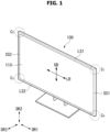
FIGS. 1 to 6 are views showing examples of a display device related to the present invention; and -
FIGS. 7 to 14 are views showing examples of a display device according to an embodiment of the present invention. - Description will now be given in detail according to exemplary embodiments disclosed herein, with reference to the accompanying drawings. For the sake of brief description with reference to the drawings, the same or equivalent components may be denoted by the same reference numbers, and description thereof will not be repeated.
- In general, suffixes such as "module" and "unit" may be used to refer to elements or components. Use of such suffixes herein is merely intended to facilitate description of the specification, and the suffixes do not have any special meaning or function. In the present disclosure, that which is well known to one of ordinary skill in the relevant art has generally been omitted for the sake of brevity. The accompanying drawings are used to assist in easy understanding of various technical features and it should be understood that the embodiments presented herein are not limited by the accompanying drawings. As such, the present disclosure should be construed to extend to any alterations, equivalents and substitutes in addition to those which are particularly set out in the accompanying drawings.
- Hereinafter, a liquid crystal display (LCD) panel will be described by way of example as a display panel; however, a display panel applicable to the present disclosure is not limited to the LCD panel, and a field emission display (FED) panel or an organic light emitting diode (OLED) panel may also be used.
- Also, in the following description, a
display device 100 may include a first long side LS1, a second long side LS2 opposite the first long side LS1, a first short side SS1 adjacent to the first long side LS1 and the second long side LS2, and a second short side SS2 opposite the first short side SS1. - Here, the first short side area SS1 may be referred to as a first side area, the second short side area SS2 may be referred to as a second side area, the first long side area LS1 may be referred to as a third side area adjacent to the first side area and the second side area and located between the first side area and the second side area, and the second long side area LS2 may be referred to as a fourth side area adjacent to the first side area and the second side area, located between the first side area and the second side area, and opposite the third side area.
- In addition, although the length of the first and second long sides LS1 and LS2 is shown and described as being greater than the length of the first and second short sides SS1 and SS2 for convenience of description, the length of the first and second long sides LS1 and LS2 may be approximately equal to the length of the first and second short sides SS1 and SS2.
- Also, in the following description, a first direction DR1 may be a direction parallel to the long sides LS1 and LS2 of the
display device 100, and a second direction DR2 may be a direction parallel to the short sides SS1 and SS2 of thedisplay device 100. A third direction DR3 may be a direction perpendicular to the first direction DR1 and/or the second direction DR2. - The first direction DR1 and the second direction DR2 may be collectively referred to as a horizontal direction. In addition, the third direction DR3 may be referred to as a vertical direction.
- The side of the
display device 100 at which an image is displayed may be referred to as a front or a front surface. The side of thedisplay device 100 at which an image is not observed when thedisplay device 100 displays the image may be referred to as a rear or a rear surface. When thedisplay device 100 is seen from the front or the front surface, the first long side portion LS1 may be referred to as an upper side or an upper surface, and the second long side portion LS2 may be referred to as a lower side or a lower surface. The first short side portion SS1 may be referred to as a right side or a right surface, and the second short side portion SS2 may be referred to as a left side or a left surface. - The first long side LS1, the second long side LS2, the first short side SS1, and the second short side SS2 may be referred to as edges of the
display device 100. In addition, the points at which the first long side LS1, the second long side LS2, the first short side SS1, and the second short side SS2 join may be referred to as corners. For example, the point at which the first long side LS1 and the first short side SS1 join may be referred to as a first corner C1, the point at which the first long side LS1 and the second short side SS2 join may be referred to as a second corner C2, the point at which the second short side SS2 and the second long side LS2 join may be referred to as a third corner C3, and the point at which the second long side LS2 and the first short side SS1 join may be referred to as a first corner C4. - Here, a direction from the first short side SS1 to the second short side SS2 or a direction from the second short side SS2 to the first short side SS1 may be referred to as a leftward-rightward direction LR. A direction from the first long side LS1 to the second long side LS2 or a direction from the second long side LS2 to the first long side LS1 may be referred to as an upward-downward direction UD.
- Referring to
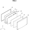
FIGS. 1 and2 , adisplay panel 110 may located at the front of thedisplay device 100, and may display an image. Thedisplay panel 110 may have a plurality of pixels, and may set hue, brightness, and saturation per pixel to output an image. - The
display panel 110 may be divided into an active area in which an image is displayed and an inactive area in which no image is displayed. Thedisplay panel 110 may include a front substrate and a rear substrate opposite each other in the state in which a liquid crystal layer is interposed therebetween. - The front substrate may include a plurality of pixels, each of which consists of red (R), green (G), and blue (B) subpixels. The front substrate may generate a color corresponding to red, green, or blue according to a control signal.
- The rear substrate may include switching elements. The rear substrate may switch a pixel electrode. For example, the pixel electrode may change the arrangement of molecules of the liquid crystal layer according to a control signal applied from the outside. The liquid crystal layer may include a plurality of liquid crystal molecules. The arrangement of the liquid crystal molecules may be changed in response to a voltage difference generated between the pixel electrode and a common electrode. The liquid crystal layer may transmit light provided by a
backlight unit 120 to the front substrate. - A
front cover 105 may cover at least a portion of the front surface and the side surface of thedisplay panel 110. Thefront cover 105 may have a hollow quadrangular frame shape. - The
front cover 105 may be divided into a front cover and a side cover. That is, thefront cover 105 may be divided into a front cover located at the front surface of thedisplay panel 110 and a side cover located at the side surface of thedisplay panel 110. The front cover and the side cover may be separately configured. One of the front cover and the side cover may be omitted. For example, only the side cover may be provided without the front cover for beautiful design, etc. - A
guide panel 117 may be located at the rear of thedisplay panel 110. Theguide panel 117 may support a portion of the rear surface of thedisplay panel 110. Theguide panel 117 may contact the contour of thedisplay panel 110. Theguide panel 117 may be coupled to aframe 130. - The
backlight unit 120 is located at the rear of thedisplay panel 110. Thebacklight unit 120 may include a plurality of light sources. Thebacklight unit 120 may be a direct type backlight unit or an edge type backlight unit. The edgetype backlight unit 120 may further include a light guide portion or a light guide panel (LGP). - The
backlight unit 120 is located at the front surface of theframe 130. For example, the plurality of light sources may be disposed at the front surface of theframe 130. In this case, thebacklight unit 120 may be a direct type backlight unit. - The
backlight unit 120 may be driven in an entire driving mode or a partial driving mode, such as a local dimming mode or an impulsive mode. Thebacklight unit 120 includes anoptical sheet 125 and may include anoptical layer 123. - The
optical sheet 125 may disperse light of the light sources. Theoptical sheet 125 may consist of a plurality of layers. For example, theoptical sheet 125 may include at least one prism sheet and/or at least one diffusion sheet. - The
optical sheet 125 may have at least onecoupling portion 125d. Thecoupling portion 125d may be coupled to thefront cover 105, theframe 130, and/or aback cover 150. That is, thecoupling portion 125d may be directly coupled to thefront cover 105, theframe 130, and/or theback cover 150. Alternatively, thecoupling portion 125d may be coupled to a structure coupled to thefront cover 105, theframe 130, and/or theback cover 150. That is, thecoupling portion 125d may be indirectly coupled to thefront cover 105, theframe 130, and/or theback cover 150. - The
optical layer 123 may include a light source. Theoptical layer 123 will be described in detail later. - The
frame 130 may support components of thedisplay device 100. For example, thebacklight unit 120 may be coupled to theframe 130. Theframe 130 may be made of a metal material, such as an aluminum alloy. - The back cover 140 may be located at the rear of the
display device 100. The back cover 140 may protect internal components from the outside. At least a portion of theback cover 150 may be coupled to theframe 130 and/or thefront cover 105. Theback cover 150 may be made of an injection-molded resin material. - Referring to
FIG. 3 , thebacklight unit 120 may include anoptical layer 123 including asubstrate 122, at least onelight assembly 124, areflection sheet 126, and adiffusion plate 129, and includes anoptical sheet 125 located in front of theoptical layer 123. - However, the components of the
backlight unit 120 are not limited thereto, and one or more of the components thereof may be omitted. - The
substrate 122 may be configured in the shape of a plurality of straps extending in a first direction and spaced apart from each other by a predetermined distance in a second direction, which is perpendicular to the first direction. - The at least one
light assembly 124 may be mounted on thesubstrate 122. An electrode pattern for connecting an adaptor and thelight assembly 124 may be formed on thesubstrate 122. For example, a carbon nanotube (CNT) pattern may be formed as the electrode pattern. - The
substrate 122 may be made of at least one of polyethylene terephthalate (PET), glass, polycarbonate (PC), or silicon. Thesubstrate 122 may be a printed circuit board (PCB). - The
light assemblies 124 may be disposed on thesubstrate 122 at predetermined intervals in the first direction. The diameter of eachlight assembly 124 may be greater than the width of thesubstrate 122. That is, the diameter of thelight assembly 124 may be greater than the length of thesubstrate 122 in the second direction. - The
light assembly 124 may be a light emitting diode (LED) chip or a light emitting diode package including at least one light emitting diode chip. - The
light assembly 124 may consist of a colored LED that emits at least one of red, blue, or green, or a white LED. The colored LED may include at least one of a red LED, a blue LED, or a green LED. - The light source included in the
light assembly 124 may be a chip on board (COB) type light source. The COB type light source may have a form in which an LED chip, as a light source, is directly coupled to thesubstrate 122. In this case, the manufacturing process may be simplified. In addition, resistance may be reduced, and therefore heat loss energy may be reduced. That is, power efficiency of thelight assembly 124 may be improved. The COB type light source may provide brighter illumination. The COB type light source may have a thickness and weight less than those of a conventional light source. - The
reflection sheet 126 may be located at the front surface of thesubstrate 122. Thereflection sheet 126 may have through-holes 235 into which the light assemblies may be inserted. - The
reflection sheet 126 may reflect light provided by thelight assemblies 124 to the front. In addition, thereflection sheet 126 may reflect light reflected by thediffusion plate 129 toward thediffusion plate 129 again. - The
reflection sheet 126 may include at least one of a metal or a metal oxide as a reflective material. For example, thereflection sheet 126 may include a metal or metal oxide that exhibits high reflectance, such as at least one of aluminum (Al), silver (Ag), gold (Au), or titanium dioxide (TiO2). - The
reflection sheet 126 may be formed by depositing or coating a metal or a metal oxide on thesubstrate 122. Ink including a metal material may be printed on thereflection sheet 126. A deposition layer may be formed on thereflection sheet 126 using a vacuum deposition method, such as a thermal deposition method, an evaporation method, or a sputtering method. A coating layer and/or a printing layer may be formed on thereflection sheet 126 using a printing method, a gravure coating method, or a silk screen method. - An air gap may be located between the
reflection sheet 126 and thediffusion plate 129. The air gap may widely spread light emitted by thelight assemblies 124. In order to maintain the air gap, asupport 200 may be located between thereflection sheet 126 and thediffusion plate 129. The air gap may be referred to as an optical gap. - A resin may be deposited on the
light assemblies 124 and/or thereflection sheet 126. The resin may diffuse light emitted by thelight assemblies 124. Thediffusion plate 129 may diffuse light emitted by thelight assemblies 124 upwards. - The
optical sheet 125 may be located in front of thediffusion plate 129. The rear surface of theoptical sheet 125 may face thediffusion plate 129, and the front surface of theoptical sheet 125 may face the rear surface of thedisplay panel 110. - The
optical sheet 125 may include at least one sheet. Specifically, theoptical sheet 125 may include at least one prism sheet and/or at least one diffusion sheet. The plurality of sheets included in theoptical sheet 125 may be in an adhered and/or tight contact state. - The
optical sheet 125 may consist of a plurality of sheets having different functions. For example, theoptical sheet 125 may include first to thirdoptical sheets 125a to 125c. The firstoptical sheet 125a may have the function of a diffusion sheet, and each of the second and thirdoptical sheets - The diffusion sheet may prevent partial concentration of light emitted from the diffusion plate such that the light is more uniformly distributed. The prism sheet may condense light emitted from the diffusion plate such that the light is incident perpendicularly on the
display panel 110. - The
coupling portions 125d may be formed at one side or at least one edge of theoptical sheet 125. Thecoupling portions 125d may be formed at at least one of the first to thirdoptical sheets 125a to 125c. - The
coupling portions 125d may be formed at the long side or the edge of theoptical sheet 125. Thecoupling portions 125d formed at the first long side and thecoupling portions 125d formed at the second long side may be asymmetric. For example, the position and/or number of thecoupling portions 125d formed at the first long side may be different from the position and/or number of thecoupling portions 125d formed at the second long side. - Referring to
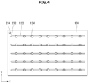
FIG. 4 , asubstrate 122 consisting of a plurality of straps extending in the first direction and spaced apart from each other by a predetermined distance in the second direction, which is perpendicular to the first direction, may be provided on theframe 130. One side of each of the plurality ofsubstrates 122 may be connected to awiring electrode 232. - The
wiring electrode 232 may extend in the second direction. Thewiring electrode 232 may be connected to one side of thesubstrate 122 in the state of being spaced apart therefrom in the second direction. - A
wiring hole 234 may be formed in one side of thewiring electrode 232. Thewiring hole 234 may be a micro-hole formed through theframe 130. Thewiring electrode 232 may extend to the rear surface of theframe 130 through thewiring hole 234. Thewiring electrode 232 may be electrically connected to an adaptor (not shown) located at the rear surface of theframe 130 through thewiring hole 234. - The
light assemblies 124 may be disposed on thesubstrate 122 at predetermined intervals in the first direction. The diameter of eachlight assembly 124 may be greater than the width of thesubstrate 122 in the second direction. - Referring to
FIG. 5 , theframe 130 includes aflat portion 132 and aninclined portion 133. Theflat portion 132 may be planar. Theinclined portion 133 extends forwards from theflat portion 132 while having a predetermined inclination relative to theflat portion 132. Theframe 130 may generally have the shape of a tub. Thereflection sheet 126 may generally have the shape of a tub so as to correspond to the shape of theframe 130. A space may be formed between theinclined portion 133 and thereflection sheet 126. - The
substrate 122 may be mounted or disposed on theflat portion 132. A plurality ofsubstrates 122 may be sequentially disposed. The plurality ofsubstrates 122 may be spaced apart from each other. For example, afirst frame 122A may extend long in the leftward-rightward direction LR of theframe 130, and may be disposed in the longitudinal direction of theframe 130. A second frame 122B may extend long in the leftward-rightward direction LR of theframe 130, and may be mounted on theframe 130 in the state of being spaced apart from thefirst frame 122A. Athird frame 122C may extend long in the leftward-rightward direction LR of theframe 130, and may be mounted on theframe 130 in the state of being spaced apart from the second frame 122B. - The distance between the
substrates 122 may be changed depending on the number of pixels of the display panel 110 (seeFIG. 2 ). For example, the distance between thesubstrates 122 necessary to provide light to a display panel 111 that realizes 8K quality may be less than the distance between thesubstrates 122 necessary to provide light to a display panel 111 that realizes 4K quality. In the case in which the number of pixels of thedisplay panel 110 is increased or image quality that can be realized by thedisplay panel 110 is increased, the light transmission ratio of thedisplay panel 110 may be reduced. To this end, a large number ofsubstrates 122 may be disposed in order to increase the luminance of light provided by the backlight unit 120 (seeFIG. 3 ). - The
reflection sheet 126 may include a plurality of through-holes 235. The plurality of through-holes 235 may correspond in number to the plurality oflight assemblies 124. Thereflection sheet 126 may be placed on theframe 130 and/or thesubstrates 122. At this time,lenses 124b of the plurality oflight assemblies 124 may be inserted into the plurality of through-holes 235 so as to protrude above thereflection sheet 126. Thereflection sheet 126 may be coupled or fixed to theframe 130 via a fixingmember 202. Thesupport 200 may be mounted on thereflection sheet 126. - Coupling
ribs inclined portion 133 of theframe 130, and thereflection sheet 126 may have coupling holes VH and HH, whereby thecoupling ribs reflection sheet 126 may be fixed to theframe 130. - The
guide panel 117 may be located at the contour of thereflection sheet 126, and may be coupled to theframe 130. Theguide panel 117 may support the display panel 110 (seeFIG. 2 ).Guide panels 117 may be located at four sides of thereflection sheet 126. - Referring to
FIG. 6 , thewiring electrode 232 extending from the front surface of theframe 130 through thewiring hole 234 may be electrically connected to apower supply 315. Thepower supply 315 may be a printed circuit board for supplying power to thedisplay device 100. Thepower supply 315 may convert AC power into DC power. - The
power supply 315 may supply current to thelight assembly 124 through thewiring electrode 232. Thepower supply 315 may be electrically connected to amain board 321 via thewiring electrode 232. Themain board 321 may be spaced apart from thepower supply 315 by a predetermined distance. - The
main board 321 may be a printed circuit board that provides an interface necessary to operate thedisplay device 100. In addition, themain board 321 may inspect and maintain the operation state of each component of thedisplay device 100. - The
main board 321 and thepower supply 315 may be electrically connected to a t-con board 319 via thewiring electrode 232. The t-con board 319 may be a printed circuit board for transmitting power or a signal input from themain board 321 or thepower supply 315 to thedisplay panel 110. The t-con board 319 may be electrically connected to thedisplay panel 110 at the front surface of theframe 130 via a flexible flat cable (FFC) 251. - The printed circuit boards are shown as being connected to each other. However, the present disclosure is not limited thereto, and only some of the printed circuit boards may be connected to each other.
- Referring to
FIG. 7 , thesupport 200 includes abase 211, abridge 213, atower 215, may include a bottom 216, and includes a fixingbar 217. The base 211 may be a plate extending long. Thebridge 213 is spaced apart from thebase 211, extends from one end to the other end of thebase 211, and may connect the one end to the other end of thebase 211. - The
bridge 213 may include afirst shoulder 2131, asecond shoulder 2132, and aloop 2133. Thefirst shoulder 2131 may extend to the upper side of the base 211 while forming an arch at one end of thebase 211. Thesecond shoulder 2132 may extend to the upper side of the base 211 while forming an arch at the other end of thebase 211. Theloop 2133 may connect thefirst shoulder 2131 and thesecond shoulder 2132 to each other. - The distance between the
first shoulder 2131 and thebase 211 and/or the distance between thesecond shoulder 2132 and the base 211 may be greater than the distance between theloop 2133 and thebase 211. That is, the upper end surface of thefirst shoulder 2131 and/or the upper end surface of thesecond shoulder 2132 may protrude further forwards than the upper surface of theloop 2133. Thefirst shoulder 2131, thesecond shoulder 2132, and/or theloop 2133 may be elastic. - The
tower 215 may extend long from the upper surface of theloop 2133. Thetower 215 may have a diameter that gradually decreases in the extension direction thereof. Thetower 215 may have a cylindrical shape. For example, thetower 215 may be elastic so as to be easily bent, or may be rigid so as not to be bent. - The bottom 216 may form a step at the lower surface of the
base 211. The step formed by the bottom 216 and the lower surface of the base 211 may correspond to the thickness of thereflection sheet 126. - The fixing
bar 217 may have ashaft 2173, includes astopper 2174, and may includebars - The
bars shaft 2173 may extend so as to protrude from the lower surface of the bottom 216 toward thebars stopper 2174 may be formed so as to protrude from the outer circumferential surface of theshaft 2173. Thestopper 2174 may be formed at opposite sides of the outer circumferential surface of theshaft 2173, or may be formed at one side thereof. A portion of a space formed by the bottom 216 and thebars stopper 2174. - Referring to
FIGS. 8 and9 , thebase 211 has a long axis CL1 in the longitudinal direction thereof. Thebars base 211. For example, the angle between the long axis CL2 of the bars and the long axis CL1 of the base 211 may be 21 degrees. - A fixing
slot 134S is formed in theflat portion 132 of theframe 130. Theframe 130 includes a fixingrecess portion 134. The fixingrecess portion 134 may be formed as the result of theframe 130 being pressed and protruding to the front of the frame. The fixingrecess portion 134 may generally have a rectangular shape. - The fixing
slot 134S may be formed by punching the fixingrecess portion 134. The fixingslot 134S may includebar slots shaft hole 1343, and astopper slot 1344. The fixingrecess portion 134 may have a long axis FL of theframe 130 in the longitudinal direction thereof. - The
bar slots bars bar slots stopper slot 1344 is tilted or form a predetermined angle relative to the long axis FL of the frame. Thestopper slot 1344 intersects thebar slots stopper slot 1344 and the long axis FL of the frame may be 21 degrees. - Protrusion holes 1345 and 1346 may be formed on the long axis CL4 of the
stopper slot 1344. Thefirst protrusion hole 1345 may be located so as to be spaced apart from one end of thestopper slot 1344, and thesecond protrusion hole 1346 may be located so as to be spaced apart from the other end of thestopper slot 1344. The protrusion holes 1345 and 1346 may be symmetrical with respect to thestopper slot 1344. - Referring to
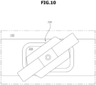
FIGS. 10 to 12 , thesupport 200 is mounted or coupled to theframe 130. Thesupport 200 may be coupled to the rear surface of the fixingrecess portion 134. Thesupport 200 is inserted into theframe 130 and rotated at the position of the fixingrecess portion 134 so as to be coupled to the frame 130 (FIGS. 10 and11 ). - The
base 211 of thesupport 200 may generally have a rectangular shape. The base 211 may have a long side and a short side. The long side of the base 211 may be defined as a longitudinal direction, and the short side of the base 211 may be defined as a lateral direction. The width D2 of the base 211 or the width D2 of the fixingrecess portion 134 may be less than the distance D1 between thesubstrates 122. The longitudinal direction of the base 211 may be parallel to the longitudinal direction of thesubstrates 122. - Consequently, it is possible to more densely dispose the
substrates 122 and the light assembles 124 and to increase the amount of light that is provided to thedisplay panel 110. - Referring to
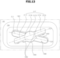
FIGS. 13 and14 , theshaft 2173 and the fixingbar 217 are inserted into the fixingslot 134S, and thesupport 200 is rotated to move the fixingbar 217 on the fixingslot 134S. The long axis CL2 of the fixingbar 217 intersects the long axis CL3 of the fixingslot 134S. Thereflection sheet 126 may be located in a space between the base 211 and the fixingrecess portion 134 formed as the bottom 216 is supported by the outer surface of the fixingrecess portion 134. The base 211 may push thereflection sheet 126, and thesupport 200 may fix thereflection sheet 126 to theframe 130. - For example, the angle between the long axis CL2 of the fixing
bar 217 and the long axis CL3 of the fixingslot 134S may be about 35 degrees. Consequently, it is possible to improve convenience when mounting and/or replacing thesupport 200. If the angle between the long axis CL2 of the fixingbar 217 and the long axis CL3 of the fixingslot 134S is less than 35 degrees, efficiency in mounting thesupport 200 to theframe 130 may be reduced, and work errors may occur. - When the fixing
bar 217 is rotated, thestopper 2174 is caught by thestopper slot 1344. Thestopper slot 1344 receives thestopper 2174 of thesupport 200, and contacts thestopper 2174 to limit the range of rotation of thesupport 200. - When the fixing
bar 217 is rotated,protrusions bar 217 may be inserted into the protrusion holes 1345 and 1346. Thefirst protrusion 2171P formed on thefirst bar 2171 may be inserted into thefirst protrusion hole 1345, and thesecond protrusion 2172P formed on thesecond bar 2172 may be inserted into thesecond protrusion hole 1346. Consequently, thesupport 200 may be securely coupled to theframe 130. - When light is provided to the
display panel 110, temperature applied to thediffusion plate 129 may increase, whereby thediffusion plate 129 may be deformed. For example, thediffusion plate 129 may droop. When thediffusion plate 129 droops, thesupport 200 may support thediffusion plate 129. The lower surface of thediffusion plate 129 may contact thetower 215 of thesupport 200. Consequently, the optical gap G may be maintained, whereby it is possible to prevent a reduction in image quality of the display device. - Certain embodiments or other embodiments of the disclosure described above are not mutually exclusive or distinct from each other. Any or all elements of the embodiments of the disclosure described above may be combined or combined with each other in configuration or function, provided they fall within the scope of the claims.
- The above-detailed description should not be interpreted restrictively in all aspects and should be considered exemplary. The scope of the present invention should be determined by a reasonable interpretation of the appended claims, all modifications within the scope of the appended claims are included within the scope of the present invention.
Claims (9)
- A display device (100) comprising:a display panel (110);a frame (130) located at a rear of the display panel;a light source (120) located between the display panel and the frame, the light source being configured to provide light to the display panel;an optical layer (125, 129) located between the display panel and the light source, the optical layer being configured to transmit the light provided by the light source; anda support (200) located between the frame and the optical layer, the support being mounted at the frame, the support being configured to support the optical layer, whereinthe support comprises:a base (211) extending long, the base being placed on the frame;a bridge (213) extending from one end to the other end of the base, the bridge being spaced apart from the base at an upper side of the base;a tower (215) extending from the bridge toward the optical layer;a shaft (2173) extending from a lower surface of the base toward the frame; anda bar (217) extending long from the shaft in a direction (CL2) intersecting a longitudinal direction (CL1) of the base, whereinthe frame (130) comprises:a flat portion (132); andan inclined portion (133) extending from the flat portion toward the display panel in a state of being inclined, andthe flat portion comprises:a fixing recess portion (134) recessed from a rear surface of the flat portion toward a front surface of the flat portion; anda bar slot (134S) formed in the fixing recess portion, the bar slot being cut out such that the bar (217) of the support passes through the bar slot, the bar slot intersecting the longitudinal direction of the base and a longitudinal direction of the bar, whereinthe support (200) further comprises a stopper (2174) formed at an outer circumferential surface of the shaft (2173), the stopper being located between the base (211) and the bar (217), andthe frame (130) further comprises a stopper slot (1344) formed in the fixing recess portion (134), the stopper slot extending long in a direction intersecting the bar slot (134S), the stopper slot (1344) being shorter than a length of the bar slot, the stopper slot corresponding to the stopper.
- The display device according to claim 1, wherein an intersection angle formed by the base (211) and the bar (217) is about 21 degrees.
- The display device according to claim 1, wherein an intersection angle formed by the base (211) and the bar slot (134S) is about 14 degrees.
- The display device according to claim 1, wherein an intersection angle formed by the bar (217) and the bar slot (134S) is about 35 degrees.
- The display device according to claim 1, wherein an intersection angle formed by the stopper slot (1344) and the bar slot (134S) is about 35 degrees.
- The display device according to claim 5, whereinthe support (200) is placed in the fixing recess portion (134), andwhen the bar (217) of the support is inserted into the bar slot (134S) and is then rotated, the stopper (2174) of the support contacts the stopper slot (1344).
- The display device according to claim 1, wherein
the frame (130) comprises:a first protrusion hole (1345) formed so as to be spaced apart from one end of the stopper slot (1344) in a longitudinal direction of the stopper slot; anda second protrusion hole (1346) formed so as to be spaced apart from the other end of the stopper slot (1344) in the longitudinal direction of the stopper slot, andthe support (200) comprises:a first protrusion (2171P) located adjacent to one end of the bar (217), the first protrusion protruding from the bar toward the base (211) so as to be inserted into the first protrusion hole (1345); anda second protrusion (2172P) located adjacent to the other end of the bar (217), the second protrusion protruding from the bar toward the base (211) so as to be inserted into the second protrusion hole (1346). - The display device according to claim 1, whereinthe support (200) further comprises a bottom (216) configured to form a step at the lower surface of the base (211) together with the lower surface of the base, andthe bottom (216) is supported at the front surface of the flat portion (132) by the fixing recess portion (134).
- The display device according to claim 8, further comprising:a reflection sheet (126) located on the frame (130), the reflection sheet being configured to reflect the light provided by the light source (120) toward the display panel (110), whereina portion of the reflection sheet is inserted into a gap formed between a front surface of the frame (130) and the lower surface of the base (211) by the bottom (216), andthe base (211) of the support (200) pushes an upper surface of the reflection sheet.
Applications Claiming Priority (1)
| Application Number | Priority Date | Filing Date | Title |
|---|---|---|---|
| PCT/KR2019/014137 WO2021080048A1 (en) | 2019-10-25 | 2019-10-25 | Display device |
Publications (3)
| Publication Number | Publication Date |
|---|---|
| EP4050407A1 EP4050407A1 (en) | 2022-08-31 |
| EP4050407A4 EP4050407A4 (en) | 2023-04-26 |
| EP4050407B1 true EP4050407B1 (en) | 2025-07-09 |
Family
ID=75585202
Family Applications (1)
| Application Number | Title | Priority Date | Filing Date |
|---|---|---|---|
| EP19949736.3A Active EP4050407B1 (en) | 2019-10-25 | 2019-10-25 | Display device |
Country Status (4)
| Country | Link |
|---|---|
| US (2) | US11169414B2 (en) |
| EP (1) | EP4050407B1 (en) |
| KR (1) | KR102638185B1 (en) |
| WO (1) | WO2021080048A1 (en) |
Families Citing this family (7)
| Publication number | Priority date | Publication date | Assignee | Title |
|---|---|---|---|---|
| WO2021080048A1 (en) | 2019-10-25 | 2021-04-29 | 엘지전자 주식회사 | Display device |
| WO2023101055A1 (en) * | 2021-12-02 | 2023-06-08 | 엘지전자 주식회사 | Display device |
| KR20250127324A (en) * | 2023-01-13 | 2025-08-26 | 엘지전자 주식회사 | display device |
| WO2024162491A1 (en) * | 2023-01-31 | 2024-08-08 | 엘지전자 주식회사 | Display device |
| KR20260028765A (en) * | 2023-07-31 | 2026-03-04 | 엘지전자 주식회사 | display device |
| WO2025150582A1 (en) * | 2024-01-10 | 2025-07-17 | 엘지전자 주식회사 | Backlight unit and display device |
| KR20250120619A (en) * | 2024-02-02 | 2025-08-11 | 삼성전자주식회사 | Display apparatus |
Family Cites Families (9)
| Publication number | Priority date | Publication date | Assignee | Title |
|---|---|---|---|---|
| KR20060087646A (en) * | 2005-01-31 | 2006-08-03 | 삼성전자주식회사 | Support member, backlight assembly having same, and display device having same |
| JP4648070B2 (en) * | 2005-04-27 | 2011-03-09 | 株式会社 日立ディスプレイズ | Display device |
| KR101306003B1 (en) * | 2006-01-03 | 2013-09-12 | 삼성디스플레이 주식회사 | Light source supporting member and display device comprising the same |
| KR101262090B1 (en) * | 2006-12-11 | 2013-05-14 | 엘지디스플레이 주식회사 | Backlight assembly for Liquid Crystal Display Device |
| KR101405595B1 (en) * | 2007-12-18 | 2014-06-12 | 엘지이노텍 주식회사 | Light emitting module connecting apparatus and light unit having the same |
| KR102297912B1 (en) * | 2015-04-29 | 2021-09-02 | 엘지전자 주식회사 | Display apparatus |
| JPWO2017038082A1 (en) * | 2015-09-01 | 2018-07-05 | パナソニックIpマネジメント株式会社 | Video display device |
| KR20170091334A (en) * | 2016-02-01 | 2017-08-09 | 엘지전자 주식회사 | Back light unit and display device comprising it |
| WO2021080048A1 (en) | 2019-10-25 | 2021-04-29 | 엘지전자 주식회사 | Display device |
-
2019
- 2019-10-25 WO PCT/KR2019/014137 patent/WO2021080048A1/en not_active Ceased
- 2019-10-25 KR KR1020227005853A patent/KR102638185B1/en active Active
- 2019-10-25 EP EP19949736.3A patent/EP4050407B1/en active Active
-
2020
- 2020-10-22 US US17/078,029 patent/US11169414B2/en active Active
-
2021
- 2021-10-06 US US17/495,762 patent/US11506936B2/en active Active
Also Published As
| Publication number | Publication date |
|---|---|
| KR20220038726A (en) | 2022-03-29 |
| US11506936B2 (en) | 2022-11-22 |
| EP4050407A1 (en) | 2022-08-31 |
| WO2021080048A1 (en) | 2021-04-29 |
| KR102638185B1 (en) | 2024-02-16 |
| US20220026767A1 (en) | 2022-01-27 |
| US20210124218A1 (en) | 2021-04-29 |
| EP4050407A4 (en) | 2023-04-26 |
| US11169414B2 (en) | 2021-11-09 |
Similar Documents
| Publication | Publication Date | Title |
|---|---|---|
| US11506936B2 (en) | Display device for enhancing backlight | |
| EP3190456B1 (en) | Display device | |
| EP3825761B1 (en) | Display device | |
| EP3447571B1 (en) | Display device | |
| KR102383645B1 (en) | Display device | |
| KR102303803B1 (en) | Display device | |
| US11966110B2 (en) | Display device | |
| EP4254057A1 (en) | Display device | |
| KR102919574B1 (en) | Display device | |
| US12372829B2 (en) | Display device | |
| KR20210017012A (en) | Display device | |
| US12044923B2 (en) | Display device | |
| KR20260028765A (en) | display device | |
| KR20210030662A (en) | Display device |
Legal Events
| Date | Code | Title | Description |
|---|---|---|---|
| STAA | Information on the status of an ep patent application or granted ep patent |
Free format text: STATUS: THE INTERNATIONAL PUBLICATION HAS BEEN MADE |
|
| PUAI | Public reference made under article 153(3) epc to a published international application that has entered the european phase |
Free format text: ORIGINAL CODE: 0009012 |
|
| STAA | Information on the status of an ep patent application or granted ep patent |
Free format text: STATUS: REQUEST FOR EXAMINATION WAS MADE |
|
| 17P | Request for examination filed |
Effective date: 20220523 |
|
| AK | Designated contracting states |
Kind code of ref document: A1 Designated state(s): AL AT BE BG CH CY CZ DE DK EE ES FI FR GB GR HR HU IE IS IT LI LT LU LV MC MK MT NL NO PL PT RO RS SE SI SK SM TR |
|
| DAV | Request for validation of the european patent (deleted) | ||
| DAX | Request for extension of the european patent (deleted) | ||
| A4 | Supplementary search report drawn up and despatched |
Effective date: 20230324 |
|
| RIC1 | Information provided on ipc code assigned before grant |
Ipc: G02F 1/13357 20060101AFI20230321BHEP |
|
| GRAP | Despatch of communication of intention to grant a patent |
Free format text: ORIGINAL CODE: EPIDOSNIGR1 |
|
| STAA | Information on the status of an ep patent application or granted ep patent |
Free format text: STATUS: GRANT OF PATENT IS INTENDED |
|
| INTG | Intention to grant announced |
Effective date: 20250210 |
|
| RAP3 | Party data changed (applicant data changed or rights of an application transferred) |
Owner name: LG ELECTRONICS INC. |
|
| GRAS | Grant fee paid |
Free format text: ORIGINAL CODE: EPIDOSNIGR3 |
|
| GRAA | (expected) grant |
Free format text: ORIGINAL CODE: 0009210 |
|
| STAA | Information on the status of an ep patent application or granted ep patent |
Free format text: STATUS: THE PATENT HAS BEEN GRANTED |
|
| AK | Designated contracting states |
Kind code of ref document: B1 Designated state(s): AL AT BE BG CH CY CZ DE DK EE ES FI FR GB GR HR HU IE IS IT LI LT LU LV MC MK MT NL NO PL PT RO RS SE SI SK SM TR |
|
| REG | Reference to a national code |
Ref country code: GB Ref legal event code: FG4D |
|
| REG | Reference to a national code |
Ref country code: CH Ref legal event code: EP |
|
| REG | Reference to a national code |
Ref country code: IE Ref legal event code: FG4D |
|
| REG | Reference to a national code |
Ref country code: DE Ref legal event code: R096 Ref document number: 602019072497 Country of ref document: DE |
|
| PGFP | Annual fee paid to national office [announced via postgrant information from national office to epo] |
Ref country code: GB Payment date: 20250909 Year of fee payment: 7 |
|
| REG | Reference to a national code |
Ref country code: NL Ref legal event code: MP Effective date: 20250709 |
|
| PG25 | Lapsed in a contracting state [announced via postgrant information from national office to epo] |
Ref country code: PT Free format text: LAPSE BECAUSE OF FAILURE TO SUBMIT A TRANSLATION OF THE DESCRIPTION OR TO PAY THE FEE WITHIN THE PRESCRIBED TIME-LIMIT Effective date: 20251110 |
|
| PG25 | Lapsed in a contracting state [announced via postgrant information from national office to epo] |
Ref country code: NL Free format text: LAPSE BECAUSE OF FAILURE TO SUBMIT A TRANSLATION OF THE DESCRIPTION OR TO PAY THE FEE WITHIN THE PRESCRIBED TIME-LIMIT Effective date: 20250709 |
|
| REG | Reference to a national code |
Ref country code: AT Ref legal event code: MK05 Ref document number: 1812363 Country of ref document: AT Kind code of ref document: T Effective date: 20250709 |
|
| PG25 | Lapsed in a contracting state [announced via postgrant information from national office to epo] |
Ref country code: IS Free format text: LAPSE BECAUSE OF FAILURE TO SUBMIT A TRANSLATION OF THE DESCRIPTION OR TO PAY THE FEE WITHIN THE PRESCRIBED TIME-LIMIT Effective date: 20251109 |
|
| PGFP | Annual fee paid to national office [announced via postgrant information from national office to epo] |
Ref country code: DE Payment date: 20250908 Year of fee payment: 7 |
|
| PG25 | Lapsed in a contracting state [announced via postgrant information from national office to epo] |
Ref country code: NO Free format text: LAPSE BECAUSE OF FAILURE TO SUBMIT A TRANSLATION OF THE DESCRIPTION OR TO PAY THE FEE WITHIN THE PRESCRIBED TIME-LIMIT Effective date: 20251009 |
|
| REG | Reference to a national code |
Ref country code: LT Ref legal event code: MG9D |
|
| PG25 | Lapsed in a contracting state [announced via postgrant information from national office to epo] |
Ref country code: AT Free format text: LAPSE BECAUSE OF FAILURE TO SUBMIT A TRANSLATION OF THE DESCRIPTION OR TO PAY THE FEE WITHIN THE PRESCRIBED TIME-LIMIT Effective date: 20250709 |
|
| PG25 | Lapsed in a contracting state [announced via postgrant information from national office to epo] |
Ref country code: FI Free format text: LAPSE BECAUSE OF FAILURE TO SUBMIT A TRANSLATION OF THE DESCRIPTION OR TO PAY THE FEE WITHIN THE PRESCRIBED TIME-LIMIT Effective date: 20250709 |
|
| PG25 | Lapsed in a contracting state [announced via postgrant information from national office to epo] |
Ref country code: HR Free format text: LAPSE BECAUSE OF FAILURE TO SUBMIT A TRANSLATION OF THE DESCRIPTION OR TO PAY THE FEE WITHIN THE PRESCRIBED TIME-LIMIT Effective date: 20250709 |
|
| PG25 | Lapsed in a contracting state [announced via postgrant information from national office to epo] |
Ref country code: GR Free format text: LAPSE BECAUSE OF FAILURE TO SUBMIT A TRANSLATION OF THE DESCRIPTION OR TO PAY THE FEE WITHIN THE PRESCRIBED TIME-LIMIT Effective date: 20251010 |
|
| PG25 | Lapsed in a contracting state [announced via postgrant information from national office to epo] |
Ref country code: SE Free format text: LAPSE BECAUSE OF FAILURE TO SUBMIT A TRANSLATION OF THE DESCRIPTION OR TO PAY THE FEE WITHIN THE PRESCRIBED TIME-LIMIT Effective date: 20250709 |
|
| PG25 | Lapsed in a contracting state [announced via postgrant information from national office to epo] |
Ref country code: LV Free format text: LAPSE BECAUSE OF FAILURE TO SUBMIT A TRANSLATION OF THE DESCRIPTION OR TO PAY THE FEE WITHIN THE PRESCRIBED TIME-LIMIT Effective date: 20250709 |
|
| PG25 | Lapsed in a contracting state [announced via postgrant information from national office to epo] |
Ref country code: BG Free format text: LAPSE BECAUSE OF FAILURE TO SUBMIT A TRANSLATION OF THE DESCRIPTION OR TO PAY THE FEE WITHIN THE PRESCRIBED TIME-LIMIT Effective date: 20250709 Ref country code: PL Free format text: LAPSE BECAUSE OF FAILURE TO SUBMIT A TRANSLATION OF THE DESCRIPTION OR TO PAY THE FEE WITHIN THE PRESCRIBED TIME-LIMIT Effective date: 20250709 |
|
| PG25 | Lapsed in a contracting state [announced via postgrant information from national office to epo] |
Ref country code: RS Free format text: LAPSE BECAUSE OF FAILURE TO SUBMIT A TRANSLATION OF THE DESCRIPTION OR TO PAY THE FEE WITHIN THE PRESCRIBED TIME-LIMIT Effective date: 20251009 |
|
| PG25 | Lapsed in a contracting state [announced via postgrant information from national office to epo] |
Ref country code: ES Free format text: LAPSE BECAUSE OF FAILURE TO SUBMIT A TRANSLATION OF THE DESCRIPTION OR TO PAY THE FEE WITHIN THE PRESCRIBED TIME-LIMIT Effective date: 20250709 |
|
| PG25 | Lapsed in a contracting state [announced via postgrant information from national office to epo] |
Ref country code: RO Free format text: LAPSE BECAUSE OF FAILURE TO SUBMIT A TRANSLATION OF THE DESCRIPTION OR TO PAY THE FEE WITHIN THE PRESCRIBED TIME-LIMIT Effective date: 20250709 |
|
| PG25 | Lapsed in a contracting state [announced via postgrant information from national office to epo] |
Ref country code: SM Free format text: LAPSE BECAUSE OF FAILURE TO SUBMIT A TRANSLATION OF THE DESCRIPTION OR TO PAY THE FEE WITHIN THE PRESCRIBED TIME-LIMIT Effective date: 20250709 |
|
| PG25 | Lapsed in a contracting state [announced via postgrant information from national office to epo] |
Ref country code: DK Free format text: LAPSE BECAUSE OF FAILURE TO SUBMIT A TRANSLATION OF THE DESCRIPTION OR TO PAY THE FEE WITHIN THE PRESCRIBED TIME-LIMIT Effective date: 20250709 |
|
| PG25 | Lapsed in a contracting state [announced via postgrant information from national office to epo] |
Ref country code: IT Free format text: LAPSE BECAUSE OF FAILURE TO SUBMIT A TRANSLATION OF THE DESCRIPTION OR TO PAY THE FEE WITHIN THE PRESCRIBED TIME-LIMIT Effective date: 20250709 |
|
| PG25 | Lapsed in a contracting state [announced via postgrant information from national office to epo] |
Ref country code: CZ Free format text: LAPSE BECAUSE OF FAILURE TO SUBMIT A TRANSLATION OF THE DESCRIPTION OR TO PAY THE FEE WITHIN THE PRESCRIBED TIME-LIMIT Effective date: 20250709 |
|
| PG25 | Lapsed in a contracting state [announced via postgrant information from national office to epo] |
Ref country code: SK Free format text: LAPSE BECAUSE OF FAILURE TO SUBMIT A TRANSLATION OF THE DESCRIPTION OR TO PAY THE FEE WITHIN THE PRESCRIBED TIME-LIMIT Effective date: 20250709 Ref country code: EE Free format text: LAPSE BECAUSE OF FAILURE TO SUBMIT A TRANSLATION OF THE DESCRIPTION OR TO PAY THE FEE WITHIN THE PRESCRIBED TIME-LIMIT Effective date: 20250709 |
|
| PLBE | No opposition filed within time limit |
Free format text: ORIGINAL CODE: 0009261 |
|
| STAA | Information on the status of an ep patent application or granted ep patent |
Free format text: STATUS: NO OPPOSITION FILED WITHIN TIME LIMIT |