EP4050387A1 - Liquid crystal cured layer transfer seal, liquid crystal cured layer transfer matter, and method for assessing authenticity of liquid crystal cured layer transfer seal - Google Patents
Liquid crystal cured layer transfer seal, liquid crystal cured layer transfer matter, and method for assessing authenticity of liquid crystal cured layer transfer seal Download PDFInfo
- Publication number
- EP4050387A1 EP4050387A1 EP20879724.1A EP20879724A EP4050387A1 EP 4050387 A1 EP4050387 A1 EP 4050387A1 EP 20879724 A EP20879724 A EP 20879724A EP 4050387 A1 EP4050387 A1 EP 4050387A1
- Authority
- EP
- European Patent Office
- Prior art keywords
- liquid crystal
- crystal cured
- cured layer
- area
- layer
- Prior art date
- Legal status (The legal status is an assumption and is not a legal conclusion. Google has not performed a legal analysis and makes no representation as to the accuracy of the status listed.)
- Pending
Links
- 239000004973 liquid crystal related substance Substances 0.000 title claims abstract description 651
- 238000012546 transfer Methods 0.000 title claims abstract description 258
- 238000000034 method Methods 0.000 title claims description 108
- 239000000758 substrate Substances 0.000 claims abstract description 247
- 150000001875 compounds Chemical class 0.000 claims abstract description 54
- 239000000203 mixture Substances 0.000 claims abstract description 54
- 239000010410 layer Substances 0.000 claims description 940
- 239000012790 adhesive layer Substances 0.000 claims description 66
- 230000003098 cholesteric effect Effects 0.000 claims description 23
- 238000005259 measurement Methods 0.000 claims description 16
- 230000002265 prevention Effects 0.000 claims description 8
- 239000004986 Cholesteric liquid crystals (ChLC) Substances 0.000 description 83
- 239000002184 metal Substances 0.000 description 23
- 239000004820 Pressure-sensitive adhesive Substances 0.000 description 22
- 239000000853 adhesive Substances 0.000 description 21
- 230000001070 adhesive effect Effects 0.000 description 21
- 239000000463 material Substances 0.000 description 19
- IUVCFHHAEHNCFT-INIZCTEOSA-N 2-[(1s)-1-[4-amino-3-(3-fluoro-4-propan-2-yloxyphenyl)pyrazolo[3,4-d]pyrimidin-1-yl]ethyl]-6-fluoro-3-(3-fluorophenyl)chromen-4-one Chemical compound C1=C(F)C(OC(C)C)=CC=C1C(C1=C(N)N=CN=C11)=NN1[C@@H](C)C1=C(C=2C=C(F)C=CC=2)C(=O)C2=CC(F)=CC=C2O1 IUVCFHHAEHNCFT-INIZCTEOSA-N 0.000 description 17
- 238000004519 manufacturing process Methods 0.000 description 15
- 229920000642 polymer Polymers 0.000 description 13
- NIXOWILDQLNWCW-UHFFFAOYSA-N acrylic acid group Chemical group C(C=C)(=O)O NIXOWILDQLNWCW-UHFFFAOYSA-N 0.000 description 12
- 238000003825 pressing Methods 0.000 description 12
- 230000015572 biosynthetic process Effects 0.000 description 8
- 239000003795 chemical substances by application Substances 0.000 description 8
- 230000000052 comparative effect Effects 0.000 description 8
- BGTOWKSIORTVQH-UHFFFAOYSA-N cyclopentanone Chemical compound O=C1CCCC1 BGTOWKSIORTVQH-UHFFFAOYSA-N 0.000 description 8
- 238000010438 heat treatment Methods 0.000 description 7
- 229920005989 resin Polymers 0.000 description 7
- 239000011347 resin Substances 0.000 description 7
- 125000002723 alicyclic group Chemical group 0.000 description 6
- 239000000047 product Substances 0.000 description 5
- 230000000694 effects Effects 0.000 description 4
- 230000001747 exhibiting effect Effects 0.000 description 4
- 239000003999 initiator Substances 0.000 description 4
- 230000000379 polymerizing effect Effects 0.000 description 4
- 239000004094 surface-active agent Substances 0.000 description 4
- 230000000007 visual effect Effects 0.000 description 4
- 229920000106 Liquid crystal polymer Polymers 0.000 description 3
- 239000004977 Liquid-crystal polymers (LCPs) Substances 0.000 description 3
- 239000004372 Polyvinyl alcohol Substances 0.000 description 3
- 238000011156 evaluation Methods 0.000 description 3
- 239000006082 mold release agent Substances 0.000 description 3
- 229920000728 polyester Polymers 0.000 description 3
- -1 polyethylene terephthalate Polymers 0.000 description 3
- 238000006116 polymerization reaction Methods 0.000 description 3
- 229920002451 polyvinyl alcohol Polymers 0.000 description 3
- 239000002356 single layer Substances 0.000 description 3
- 229920005992 thermoplastic resin Polymers 0.000 description 3
- UWCWUCKPEYNDNV-LBPRGKRZSA-N 2,6-dimethyl-n-[[(2s)-pyrrolidin-2-yl]methyl]aniline Chemical compound CC1=CC=CC(C)=C1NC[C@H]1NCCC1 UWCWUCKPEYNDNV-LBPRGKRZSA-N 0.000 description 2
- 239000004952 Polyamide Substances 0.000 description 2
- 239000003522 acrylic cement Substances 0.000 description 2
- YPHMISFOHDHNIV-FSZOTQKASA-N cycloheximide Chemical compound C1[C@@H](C)C[C@H](C)C(=O)[C@@H]1[C@H](O)CC1CC(=O)NC(=O)C1 YPHMISFOHDHNIV-FSZOTQKASA-N 0.000 description 2
- 238000010894 electron beam technology Methods 0.000 description 2
- 238000010884 ion-beam technique Methods 0.000 description 2
- 238000003475 lamination Methods 0.000 description 2
- 230000003287 optical effect Effects 0.000 description 2
- 239000000049 pigment Substances 0.000 description 2
- 229920002647 polyamide Polymers 0.000 description 2
- 229920006254 polymer film Polymers 0.000 description 2
- 229920001296 polysiloxane Polymers 0.000 description 2
- 238000002360 preparation method Methods 0.000 description 2
- 238000010298 pulverizing process Methods 0.000 description 2
- 238000007650 screen-printing Methods 0.000 description 2
- 239000002904 solvent Substances 0.000 description 2
- 238000003860 storage Methods 0.000 description 2
- 229920006302 stretch film Polymers 0.000 description 2
- 239000000126 substance Substances 0.000 description 2
- 238000004381 surface treatment Methods 0.000 description 2
- 238000012360 testing method Methods 0.000 description 2
- 238000002834 transmittance Methods 0.000 description 2
- XLYOFNOQVPJJNP-UHFFFAOYSA-N water Substances O XLYOFNOQVPJJNP-UHFFFAOYSA-N 0.000 description 2
- JOYRKODLDBILNP-UHFFFAOYSA-N Ethyl urethane Chemical compound CCOC(N)=O JOYRKODLDBILNP-UHFFFAOYSA-N 0.000 description 1
- 239000004962 Polyamide-imide Substances 0.000 description 1
- 239000004695 Polyether sulfone Substances 0.000 description 1
- 239000004697 Polyetherimide Substances 0.000 description 1
- 239000004642 Polyimide Substances 0.000 description 1
- 239000004793 Polystyrene Substances 0.000 description 1
- 238000010521 absorption reaction Methods 0.000 description 1
- DQXBYHZEEUGOBF-UHFFFAOYSA-N but-3-enoic acid;ethene Chemical compound C=C.OC(=O)CC=C DQXBYHZEEUGOBF-UHFFFAOYSA-N 0.000 description 1
- 239000006227 byproduct Substances 0.000 description 1
- 229920002301 cellulose acetate Polymers 0.000 description 1
- 238000013329 compounding Methods 0.000 description 1
- 238000013461 design Methods 0.000 description 1
- 239000005038 ethylene vinyl acetate Substances 0.000 description 1
- 239000004744 fabric Substances 0.000 description 1
- 238000007646 gravure printing Methods 0.000 description 1
- 238000007641 inkjet printing Methods 0.000 description 1
- 238000010030 laminating Methods 0.000 description 1
- 239000010985 leather Substances 0.000 description 1
- 238000012986 modification Methods 0.000 description 1
- 230000004048 modification Effects 0.000 description 1
- 238000007645 offset printing Methods 0.000 description 1
- 238000004806 packaging method and process Methods 0.000 description 1
- 229920001200 poly(ethylene-vinyl acetate) Polymers 0.000 description 1
- 229920002492 poly(sulfone) Polymers 0.000 description 1
- 229920002312 polyamide-imide Polymers 0.000 description 1
- 229920001230 polyarylate Polymers 0.000 description 1
- 239000004417 polycarbonate Substances 0.000 description 1
- 229920000515 polycarbonate Polymers 0.000 description 1
- 229920006393 polyether sulfone Polymers 0.000 description 1
- 229920001601 polyetherimide Polymers 0.000 description 1
- 229920000139 polyethylene terephthalate Polymers 0.000 description 1
- 239000005020 polyethylene terephthalate Substances 0.000 description 1
- 229920001721 polyimide Polymers 0.000 description 1
- 229920000193 polymethacrylate Polymers 0.000 description 1
- 229920000098 polyolefin Polymers 0.000 description 1
- 229920002223 polystyrene Polymers 0.000 description 1
- 239000004800 polyvinyl chloride Substances 0.000 description 1
- 229920000915 polyvinyl chloride Polymers 0.000 description 1
- 238000007639 printing Methods 0.000 description 1
- 238000009877 rendering Methods 0.000 description 1
- 238000000926 separation method Methods 0.000 description 1
- 238000012719 thermal polymerization Methods 0.000 description 1
Images




Classifications
-
- G—PHYSICS
- G09—EDUCATION; CRYPTOGRAPHY; DISPLAY; ADVERTISING; SEALS
- G09F—DISPLAYING; ADVERTISING; SIGNS; LABELS OR NAME-PLATES; SEALS
- G09F9/00—Indicating arrangements for variable information in which the information is built-up on a support by selection or combination of individual elements
- G09F9/30—Indicating arrangements for variable information in which the information is built-up on a support by selection or combination of individual elements in which the desired character or characters are formed by combining individual elements
- G09F9/35—Indicating arrangements for variable information in which the information is built-up on a support by selection or combination of individual elements in which the desired character or characters are formed by combining individual elements being liquid crystals
-
- B—PERFORMING OPERATIONS; TRANSPORTING
- B42—BOOKBINDING; ALBUMS; FILES; SPECIAL PRINTED MATTER
- B42D—BOOKS; BOOK COVERS; LOOSE LEAVES; PRINTED MATTER CHARACTERISED BY IDENTIFICATION OR SECURITY FEATURES; PRINTED MATTER OF SPECIAL FORMAT OR STYLE NOT OTHERWISE PROVIDED FOR; DEVICES FOR USE THEREWITH AND NOT OTHERWISE PROVIDED FOR; MOVABLE-STRIP WRITING OR READING APPARATUS
- B42D25/00—Information-bearing cards or sheet-like structures characterised by identification or security features; Manufacture thereof
- B42D25/30—Identification or security features, e.g. for preventing forgery
- B42D25/36—Identification or security features, e.g. for preventing forgery comprising special materials
- B42D25/364—Liquid crystals
-
- B—PERFORMING OPERATIONS; TRANSPORTING
- B42—BOOKBINDING; ALBUMS; FILES; SPECIAL PRINTED MATTER
- B42D—BOOKS; BOOK COVERS; LOOSE LEAVES; PRINTED MATTER CHARACTERISED BY IDENTIFICATION OR SECURITY FEATURES; PRINTED MATTER OF SPECIAL FORMAT OR STYLE NOT OTHERWISE PROVIDED FOR; DEVICES FOR USE THEREWITH AND NOT OTHERWISE PROVIDED FOR; MOVABLE-STRIP WRITING OR READING APPARATUS
- B42D25/00—Information-bearing cards or sheet-like structures characterised by identification or security features; Manufacture thereof
- B42D25/30—Identification or security features, e.g. for preventing forgery
- B42D25/351—Translucent or partly translucent parts, e.g. windows
-
- B—PERFORMING OPERATIONS; TRANSPORTING
- B42—BOOKBINDING; ALBUMS; FILES; SPECIAL PRINTED MATTER
- B42D—BOOKS; BOOK COVERS; LOOSE LEAVES; PRINTED MATTER CHARACTERISED BY IDENTIFICATION OR SECURITY FEATURES; PRINTED MATTER OF SPECIAL FORMAT OR STYLE NOT OTHERWISE PROVIDED FOR; DEVICES FOR USE THEREWITH AND NOT OTHERWISE PROVIDED FOR; MOVABLE-STRIP WRITING OR READING APPARATUS
- B42D25/00—Information-bearing cards or sheet-like structures characterised by identification or security features; Manufacture thereof
- B42D25/30—Identification or security features, e.g. for preventing forgery
- B42D25/36—Identification or security features, e.g. for preventing forgery comprising special materials
- B42D25/378—Special inks
- B42D25/391—Special inks absorbing or reflecting polarised light
-
- B—PERFORMING OPERATIONS; TRANSPORTING
- B42—BOOKBINDING; ALBUMS; FILES; SPECIAL PRINTED MATTER
- B42D—BOOKS; BOOK COVERS; LOOSE LEAVES; PRINTED MATTER CHARACTERISED BY IDENTIFICATION OR SECURITY FEATURES; PRINTED MATTER OF SPECIAL FORMAT OR STYLE NOT OTHERWISE PROVIDED FOR; DEVICES FOR USE THEREWITH AND NOT OTHERWISE PROVIDED FOR; MOVABLE-STRIP WRITING OR READING APPARATUS
- B42D25/00—Information-bearing cards or sheet-like structures characterised by identification or security features; Manufacture thereof
- B42D25/40—Manufacture
-
- B—PERFORMING OPERATIONS; TRANSPORTING
- B42—BOOKBINDING; ALBUMS; FILES; SPECIAL PRINTED MATTER
- B42D—BOOKS; BOOK COVERS; LOOSE LEAVES; PRINTED MATTER CHARACTERISED BY IDENTIFICATION OR SECURITY FEATURES; PRINTED MATTER OF SPECIAL FORMAT OR STYLE NOT OTHERWISE PROVIDED FOR; DEVICES FOR USE THEREWITH AND NOT OTHERWISE PROVIDED FOR; MOVABLE-STRIP WRITING OR READING APPARATUS
- B42D25/00—Information-bearing cards or sheet-like structures characterised by identification or security features; Manufacture thereof
- B42D25/40—Manufacture
- B42D25/45—Associating two or more layers
- B42D25/465—Associating two or more layers using chemicals or adhesives
- B42D25/47—Associating two or more layers using chemicals or adhesives using adhesives
-
- B—PERFORMING OPERATIONS; TRANSPORTING
- B44—DECORATIVE ARTS
- B44C—PRODUCING DECORATIVE EFFECTS; MOSAICS; TARSIA WORK; PAPERHANGING
- B44C1/00—Processes, not specifically provided for elsewhere, for producing decorative surface effects
- B44C1/16—Processes, not specifically provided for elsewhere, for producing decorative surface effects for applying transfer pictures or the like
- B44C1/165—Processes, not specifically provided for elsewhere, for producing decorative surface effects for applying transfer pictures or the like for decalcomanias; sheet material therefor
- B44C1/17—Dry transfer
- B44C1/1704—Decalcomanias provided with a particular decorative layer, e.g. specially adapted to allow the formation of a metallic or dyestuff layer on a substrate unsuitable for direct deposition
-
- G—PHYSICS
- G02—OPTICS
- G02B—OPTICAL ELEMENTS, SYSTEMS OR APPARATUS
- G02B5/00—Optical elements other than lenses
- G02B5/30—Polarising elements
- G02B5/3016—Polarising elements involving passive liquid crystal elements
-
- G—PHYSICS
- G02—OPTICS
- G02F—OPTICAL DEVICES OR ARRANGEMENTS FOR THE CONTROL OF LIGHT BY MODIFICATION OF THE OPTICAL PROPERTIES OF THE MEDIA OF THE ELEMENTS INVOLVED THEREIN; NON-LINEAR OPTICS; FREQUENCY-CHANGING OF LIGHT; OPTICAL LOGIC ELEMENTS; OPTICAL ANALOGUE/DIGITAL CONVERTERS
- G02F1/00—Devices or arrangements for the control of the intensity, colour, phase, polarisation or direction of light arriving from an independent light source, e.g. switching, gating or modulating; Non-linear optics
- G02F1/01—Devices or arrangements for the control of the intensity, colour, phase, polarisation or direction of light arriving from an independent light source, e.g. switching, gating or modulating; Non-linear optics for the control of the intensity, phase, polarisation or colour
- G02F1/13—Devices or arrangements for the control of the intensity, colour, phase, polarisation or direction of light arriving from an independent light source, e.g. switching, gating or modulating; Non-linear optics for the control of the intensity, phase, polarisation or colour based on liquid crystals, e.g. single liquid crystal display cells
- G02F1/133—Constructional arrangements; Operation of liquid crystal cells; Circuit arrangements
- G02F1/1333—Constructional arrangements; Manufacturing methods
- G02F1/1334—Constructional arrangements; Manufacturing methods based on polymer dispersed liquid crystals, e.g. microencapsulated liquid crystals
-
- G—PHYSICS
- G07—CHECKING-DEVICES
- G07D—HANDLING OF COINS OR VALUABLE PAPERS, e.g. TESTING, SORTING BY DENOMINATIONS, COUNTING, DISPENSING, CHANGING OR DEPOSITING
- G07D7/00—Testing specially adapted to determine the identity or genuineness of valuable papers or for segregating those which are unacceptable, e.g. banknotes that are alien to a currency
- G07D7/06—Testing specially adapted to determine the identity or genuineness of valuable papers or for segregating those which are unacceptable, e.g. banknotes that are alien to a currency using wave or particle radiation
- G07D7/12—Visible light, infrared or ultraviolet radiation
- G07D7/1205—Testing spectral properties
-
- G—PHYSICS
- G02—OPTICS
- G02F—OPTICAL DEVICES OR ARRANGEMENTS FOR THE CONTROL OF LIGHT BY MODIFICATION OF THE OPTICAL PROPERTIES OF THE MEDIA OF THE ELEMENTS INVOLVED THEREIN; NON-LINEAR OPTICS; FREQUENCY-CHANGING OF LIGHT; OPTICAL LOGIC ELEMENTS; OPTICAL ANALOGUE/DIGITAL CONVERTERS
- G02F1/00—Devices or arrangements for the control of the intensity, colour, phase, polarisation or direction of light arriving from an independent light source, e.g. switching, gating or modulating; Non-linear optics
- G02F1/01—Devices or arrangements for the control of the intensity, colour, phase, polarisation or direction of light arriving from an independent light source, e.g. switching, gating or modulating; Non-linear optics for the control of the intensity, phase, polarisation or colour
- G02F1/13—Devices or arrangements for the control of the intensity, colour, phase, polarisation or direction of light arriving from an independent light source, e.g. switching, gating or modulating; Non-linear optics for the control of the intensity, phase, polarisation or colour based on liquid crystals, e.g. single liquid crystal display cells
- G02F1/133—Constructional arrangements; Operation of liquid crystal cells; Circuit arrangements
- G02F1/1333—Constructional arrangements; Manufacturing methods
- G02F1/1334—Constructional arrangements; Manufacturing methods based on polymer dispersed liquid crystals, e.g. microencapsulated liquid crystals
- G02F1/13345—Network or three-dimensional gels
Definitions
- the present invention relates to a liquid crystal cured layer transfer sticker, a liquid crystal cured layer transferred article, and a method for determining the authenticity of the liquid crystal cured layer transfer sticker.
- An unauthorized use prevention body including a substrate film, an authenticity determination layer adhering to the substrate film, and an adhesive layer is known (Patent Literature 1).
- An example of the authenticity determination layer being used is a polymer film in which an oriented state of a liquid crystal compound is fixed. By attaching the unauthorized use prevention body to an adherend and peeling off the substrate film, the polymer film is destroyed, and a certain pattern is displayed.
- Patent Literature 1 Japanese Patent Application Laid-open No. 2002-205472 A
- a layer made by curing a liquid crystal composition containing a polymerizable liquid crystal compound may be made into a layer having various functions by adjusting the type of the liquid crystal composition, the method for producing the layer, and the like.
- One method for forming a layer having such a function on an adherend in a pattern is a method of peeling off the liquid crystal cured layer from the substrate, pulverizing it to produce flake-shaped pigment, and printing ink containing the pigment onto the adherend.
- such a method requires complicated steps such as a peeling step and a pulverizing step.
- the adherend with the liquid crystal cured layer transferred can be constituted as, e.g., an article having excellent design, and it can also prove that,.e.g., the adherend is an authentic article.
- liquid crystal cured layer transfer sticker that can transfer a liquid crystal cured layer onto an adherend in a pattern with a clear outline; a liquid crystal cured layer transferred article including the adherend and the liquid crystal cured layer transferred by the liquid crystal cured layer transfer sticker; and a method for determining the authenticity of the liquid crystal cured layer transfer sticker.
- liquid crystal cured layer transfer sticker with a specific configuration including a substrate, a liquid crystal cured layer, and a pattern layer to complete the present invention.
- the present invention provides the following:
- the present invention can provide a liquid crystal cured layer transfer sticker that can transfer a liquid crystal cured layer onto an adherend in a pattern with a clear outline; a liquid crystal cured layer transferred article including the adherend and the liquid crystal cured layer transferred by the liquid crystal cured layer transfer sticker; and a method for determining the authenticity of the liquid crystal cured layer transfer sticker.
- nx represents a refractive index in a direction that, among directions perpendicular to a thickness direction of the layer (the in-plane directions), gives the largest refractive index.
- ny represents a refractive index the direction being orthogonal to the direction of nx among the aforementioned in-plane directions of the layer.
- the letter d represents the thickness of the layer.
- the measurement wavelength is 550 nm, unless otherwise specified.
- the direction of a component being "parallel” and “orthogonal” may include errors within a range not impairing the effect of the present invention, for example, within a range of ⁇ 3°, ⁇ 2° or ⁇ 1°, unless otherwise specified.
- a " ⁇ /2 plate” and a “ ⁇ /4 plate” include not only rigid members but also flexible members such as resin films, unless otherwise specified.
- an adhesive includes not only adhesives in a narrow sense (adhesives with a shear storage modulus at 23°C after energy ray application or heat treatment of 1 MPa to 500 MPa) but also sticky agent with a shear storage modulus at 23°C of less than 1 MPa, unless otherwise specified.
- a liquid crystal cured layer transfer sticker includes a substrate, a liquid crystal cured layer in contact with the substrate through one face S1, and a pattern layer in contact with a partial area F in another face S2 of the liquid crystal cured layer.
- the face S2 of the liquid crystal cured layer is divided by a plurality of incisions, and the pattern layer is a layer having adhesiveness or the pattern layer is a layer having peelability.
- the pattern layer does not cover the entire face S2 of the liquid crystal cured layer and does not exist on an area G that is other than the area F of the face S2.
- FIG. 1 is an exploded perspective view schematically illustrating the liquid crystal cured layer transfer sticker according to a first embodiment of the present invention.
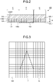
- FIG. 2 is a sectional view schematically illustrating the liquid crystal cured layer transfer sticker according to the first embodiment of the present invention.
- FIG. 3 is a schematic view of a liquid crystal cured layer according to the first embodiment of the present invention when viewed in a thickness direction.
- this liquid crystal cured layer transfer sticker 100 of the present embodiment includes a substrate 110, a liquid crystal cured layer 120, and a pattern layer 130.
- the substrate 110 is preferably a transparent substrate.
- a face 120U as the one face S1 of the liquid crystal cured layer 120 is in contact with one face 110D of the substrate 110.
- One face 130U of the pattern layer 130 is in contact with the partial area F in a face 120D that is the other face S2 of the liquid crystal cured layer 120.
- the area G is an area other than the area F of the liquid crystal cured layer 120.
- the face 120D of the liquid crystal cured layer 120 is divided by a plurality of incisions 121.
- a depth 121DP of the incisions 121 is the same as a thickness d of the liquid crystal cured layer 120.
- the plurality of the incisions 121 reach the face 120U of the liquid crystal cured layer 120 to divide the face 120U.
- the depth 121DP of the incisions 121 is the same as the thickness d; however, in another embodiment, the depth 121DP of the incisions may be d or less.
- the depth 121DP of the plurality of the incisions is preferably 0.1d or more, more preferably 0.2d or more, even more preferably 0.3d or more, particularly preferably 0.4d or more, most preferably 0.5d or more, larger than 0.5d, 0.7d or more, or 0.8d or more, and usually d or less, for example.
- the depth 121DP of the plurality of the incisions being the aforementioned lower limit value or more, when the substrate 110 of the liquid crystal cured layer transfer sticker 100 is peeled off, the outline of a partial area of the liquid crystal cured layer 120 transferred to an adherend becomes clearer. In addition, falsification of the liquid crystal cured layer transfer sticker 100 can effectively be prevented.
- the incisions 121 are formed over the entire face 120D of the liquid crystal cured layer 120 and are formed in a grid shape when viewed in the thickness direction of the liquid crystal cured layer 120.
- a length 122L of one edge of the grid is preferably 5 ⁇ m or more and more preferably 50 ⁇ m or more and preferably 100 ⁇ m or less and more preferably 70 ⁇ m or less. With the length 122L being the aforementioned lower limit value or more, the plurality of the incisions 121 can easily be formed in the liquid crystal cured layer 120.
- the length 122L being the aforementioned upper limit value or less
- the outline of the partial area of the liquid crystal cured layer 120 transferred to the adherend becomes smoother.
- the pattern layer 130 serves as a character pattern
- the transferred partial area of the liquid crystal cured layer 120 serves as a character pattern
- determination of the character becomes easier.
- falsification of the liquid crystal cured layer transfer sticker 100 can be prevented more effectively.
- the plurality of the incisions 121 may be of any shape such as a shape of lines parallel to each other, a honeycomb shape, or a shape of a group of triangles when viewed in the thickness direction of the liquid crystal cured layer 120.
- the plurality of the incisions 121 may be formed on the entire face 120D of the liquid crystal cured layer 120 or be formed only in part of the face 120D (the surrounding area of the area F, for example).
- the liquid crystal cured layer transfer sticker includes the substrate, the liquid crystal cured layer in contact with the substrate through the one face S1, the pattern layer in contact with the partial area F in the other face S2 of the liquid crystal cured layer, and an adhesive layer further covering the face S2 of the liquid crystal cured layer and the pattern layer.
- the face S2 of the liquid crystal cured layer is divided by the plurality of the incisions, and the pattern layer is a layer having peelability.
- the pattern layer does not cover the entire face S2 of the liquid crystal cured layer and does not exist on the area G, which is other than the area F of the face S2.
- FIG. 4 is an exploded perspective view schematically illustrating the liquid crystal cured layer transfer sticker according to a second embodiment of the present invention.
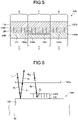
- FIG. 5 is a sectional view schematically illustrating the liquid crystal cured layer transfer sticker according to the second embodiment of the present invention.
- this liquid crystal cured layer transfer sticker 200 of the present embodiment includes the substrate 110, the liquid crystal cured layer 120, a pattern layer 230, and an adhesive layer 240.
- the substrate 110 and the liquid crystal cured layer 120 have the same configuration as the substrate 110 and the liquid crystal cured layer 120 included in the liquid crystal cured layer transfer sticker 100, and thus descriptions thereof are partially omitted.
- the pattern layer 230 is a layer having peelability. As illustrated in FIG. 5 , one face 230U of the pattern layer 230 is in contact with the partial area F of the face 120D of the liquid crystal cured layer 120. A partial area G' in one face 240U of the adhesive layer 240 is in contact with the area G, which is the area other than the area F.
- the other face 230D of the pattern layer 230 is in contact with an area F'.
- the area F' is an area other than the partial area G' of the face 240U of the adhesive layer 240. That is, the adhesive layer 240 covers the area G in the face 120D as the face S2 of the liquid crystal cured layer 120 and the face 230D of the pattern layer 230.
- the liquid crystal cured layer transfer sticker 200 is attached to the adherend, and then the substrate 110 is peeled off from the liquid crystal cured layer transfer sticker 200, in a portion in which the substrate 110, the liquid crystal cured layer 120, and the adhesive layer 240 are laminated on one another in this order (that is, a portion including the area G of the liquid crystal cured layer 120), the liquid crystal cured layer 120 and the adhesive layer 240 are hard to peel off from each other, whereas the substrate 110 and the liquid crystal cured layer 120 are easily peeled off from each other.
- the liquid crystal cured layer transfer sticker 200 is attached to the adherend, and then the substrate 110 is peeled off from the liquid crystal cured layer transfer sticker 200, in a portion in which the substrate 110, the liquid crystal cured layer 120, the pattern layer 230, and the adhesive layer 240 are laminated on one another in this order (that is, a portion including the area F of the liquid crystal cured layer 120), at least either the liquid crystal cured layer 120 and the pattern layer 230 or the pattern layer 230 and the adhesive layer 240 are easily peeled off from each other, whereas the substrate 110 and the liquid crystal cured layer 120 are hard to peel off from each other.
- the liquid crystal cured layer transfer sticker 200 can easily be separated into a first member including the substrate 110 and the area F of the liquid crystal cured layer 120 and a second member including the adhesive layer 240 adhering to the adherend and the area G of the liquid crystal cured layer 120.
- the pattern layer 230 may be included in the first member when C > D and be included in the second member when C ⁇ D.
- the liquid crystal cured layer transfer sticker 200 can be made to satisfy the condition (i). Adjustment of the adhesiveness of the adhesive layer 240 may be effected by changing the type of the adhesive forming the adhesive layer 240 as appropriate, for example.
- the liquid crystal cured layer transfer sticker 200 can be made to satisfy the condition (ii).
- the following description of the components is applicable to each of the components of the liquid crystal cured layer transfer sticker according to the first embodiment, the liquid crystal cured layer transfer sticker according to the second embodiment, and liquid crystal cured layer transfer stickers that are the modifications thereof.
- the substrate is usually a film formed of a material having flexibility.
- the substrate is preferably a transparent substrate.
- the substrate being transparent usually means that the total light transmittance of the substrate is 70% or more.
- the total light transmittance of the substrate is usually 100% or less.
- thermoplastic resins examples include thermoplastic resins.
- the thermoplastic resin usually contains a polymer.
- the polymer contained in the thermoplastic resin may include polyolefins; alicyclic structure-containing polymers; polycarbonates; polyesters such as polyethylene terephthalate; polysulfone; polyethersulfone; polystyrene; polyvinyl alcohol; cellulose acetate; polyvinyl chloride; and polymethacrylate.
- alicyclic structure-containing polymers are preferred from the viewpoint of transparency, low moisture absorption property, size stability, and processability.
- the alicyclic structure-containing polymer is a polymer having an alicyclic structure in a main chain and/or a side chain. Examples thereof for use may include those described in Japanese Patent Application Laid-open No. 2007-057971 A .
- Examples of the resin containing the alicyclic structure-containing polymer may include "ZEONOR” manufactured by ZEON CORPORATION.
- the resin one containing one type of polymer alone may be used or one containing two or more types of polymers in combination in any ratio may be used.
- the resin may also contain any compounding agents so long as they do not significantly impair the effect of the present invention.
- the substrate may have a single-layer structure including only one layer or have a multilayer structure including two or more layers.
- the substrate may have an orientation film, for example.
- the orientation film may be formed of a resin containing a polymer such as polyimide, polyvinyl alcohol, polyester, polyarylate, polyamide-imide, polyetherimide, or polyamide, for example.
- a polymer such as polyimide, polyvinyl alcohol, polyester, polyarylate, polyamide-imide, polyetherimide, or polyamide, for example.
- One type of these polymers may be used alone or two or more types thereof may be used in combination in any ratio.
- the substrate may be subjected to surface treatment.
- the surface treatment may include treatment to promote the orientation of a liquid crystal compound such as rubbing treatment, orientation film formation treatment, stretching treatment, or ion beam orientation treatment.
- the substrate may be an unstretched film, which has not been stretched, or a stretched film, which has been stretched.
- the substrate may be a layer having optical anisotropy or a layer having optical isotropy.
- the substrate has a retardation at a measurement wavelength of 550 nm in the in-plane direction of preferably 30 nm or less, more preferably 20 nm or less, even more preferably 10 nm or less, usually 0 nm or more, and possibly 0 nm.
- the substrate preferably has a capability of functioning as a 1/2 wavelength plate (a ⁇ /2 plate).
- the substrate has a retardation at a measurement wavelength of 550 nm in the in-plane direction of preferably (550n/2 - 50) nm or more and more preferably (550n/2 - 30) nm or more and preferably (550n/2 + 50) nm or less and more preferably (550n/2 + 30) nm or less.
- the letter n is an odd number of 1 or more.
- the letter n is preferably 1 or 3 and more preferably 1.
- the substrate has a capability of functioning as the ⁇ /2 plate, a plurality of ways to determine whether the liquid crystal cured layer transfer sticker is authentic are available, and thus falsification of the liquid crystal cured layer transfer sticker can be prevented more effectively.
- the substrate may be of any thickness.
- the thickness of the substrate may be 30 ⁇ m or more and 50 ⁇ m or more, for example, and 1,000 ⁇ m or less and 500 ⁇ m or less, for example.
- the liquid crystal cured layer is a layer obtained by curing a liquid crystal composition containing a polymerizable liquid crystal compound.
- the polymerizable liquid crystal compound is a liquid crystal compound that is capable of polymerizing in a liquid crystal composition while exhibiting a liquid crystal phase and become a polymer while maintaining the orientation of molecules in the liquid crystal phase.
- the polymerizable liquid crystal compound may include liquid crystal compounds having a polymerizable group, compounds that is capable of forming side-chain liquid crystal polymers, and disk-shaped liquid crystal compounds.
- Specific examples of the liquid crystal compounds having a polymerizable group may include rod-shaped liquid crystal compounds having a polymerizable group described in Japanese Patent Application Laid-open No. H11-513360 A , Japanese Patent Application Laid-open No. 2002-030042 A , Japanese Patent Application Laid-open No.
- side-chain liquid crystal polymer compounds may include side-chain liquid crystal polymer compounds described in Japanese Patent Application Laid-open No. 2003-177242 A and the like.
- preferred polymerizable liquid crystal compounds by product name may include "LC242" manufactured by BASF.
- disk-shaped liquid crystal compounds may include disk-shaped liquid crystal compounds described in Japanese Patent Application Laid-open No. H08-50206 A .
- the liquid crystal cured layer preferably has cholesteric regularity.
- Cholesteric regularity is a structure in which the angles of molecular axes in stacking planes are shifted (twisted) as the planes are observed sequentially passing through the stacked planes, such that molecular axes in a certain plane are oriented in a constant direction, molecular axes in a subsequent plain stacking thereon are oriented in a direction shifted by a small angle with respect to that of the certain plane, and molecular axes in still another plane are oriented in a direction of a further shifted angle.
- the molecules in a certain first plane inside the layer are arrayed such that the molecular axes are oriented in a constant direction.
- the direction of the molecular axes shifts at a slight angle with respect to the direction of the molecular axes in the first plane.
- the direction of the molecular axes further shifts at an angle from the direction of the molecular axes in the second plane.
- the angle of the molecular axes in the planes successively shifts (twists) in the planes arranged in a stacked manner.
- Such a structure in which the direction of the molecular axes twists is usually a helical structure, which is an optically chiral structure.
- the liquid crystal cured layer having cholesteric regularity is capable of separating clockwise and counterclockwise circularly polarized light. That is, this layer has a property of allowing one circularly polarized light of clockwise circularly polarized light and counterclockwise circularly polarized light to pass therethrough, and reflecting part or the entirety of the other circularly polarized light. Reflection in the liquid crystal cured layer having cholesteric regularity reflects circularly polarized light while maintaining its chirality.
- the liquid crystal cured layer having cholesteric regularity is also referred to as a cholesteric liquid crystal cured layer in the following.
- the cholesteric liquid crystal cured layer preferably has a high reflectance in a reflection wavelength range wherein the one circularly polarized light among the clockwise circularly polarized light and the counterclockwise circularly polarized light is allowed to pass therethrough and at least part of the other circularly polarized light is reflected from the viewpoint of increasing the difference in color observed during authenticity determination to facilitate the determination.
- the cholesteric liquid crystal cured layer preferably has a reflection wavelength range giving a reflectance of 40% or more for unpolarized light incidence.
- the cholesteric liquid crystal cured layer may have a single-layer structure or have a multilayer structure of two or more layers.
- the number of layers included in the cholesteric liquid crystal cured layer is preferably 1 to 100 and more preferably 1 to 20 from the viewpoint of ease of production.
- Examples of the method for forming the cholesteric liquid crystal cured layer may include a method of providing a layer of a cholesteric liquid crystal composition on the substrate and curing the aforementioned layer to obtain the cholesteric liquid crystal cured layer.
- the material referred to as the "liquid crystal composition” encompasses not only mixtures of two or more substances but also materials consisting of a single substance.
- the cholesteric liquid crystal composition refers to a composition in which when a liquid crystal compound contained in the liquid crystal composition is oriented, the liquid crystal compound is capable of exhibiting a liquid crystal phase having cholesteric regularity (a cholesteric liquid crystal phase).
- the cholesteric liquid crystal composition a liquid crystal composition containing a polymerizable liquid crystal compound and further containing optional components as needed may be used.
- the polymerizable liquid crystal compound By using the polymerizable liquid crystal compound, the cholesteric liquid crystal cured layer can have high thermal stability.
- the layer of the cholesteric liquid crystal composition By polymerizing the polymerizable liquid crystal compound while exhibiting cholesteric regularity, the layer of the cholesteric liquid crystal composition can be cured to obtain a non-liquid crystal cholesteric liquid crystal cured layer that is cured while exhibiting cholesteric regularity.
- the cholesteric liquid crystal composition those described in WO 2016/002765 may be used, for example.
- the cholesteric liquid crystal composition it is preferable to use a composition containing one or more compounds selected from the compounds (A1) to (A10) shown below and one or more rod-shaped liquid crystal compounds selected from the compounds (B1) to (B9) shown below, and it is more preferable to use a composition containing the compound (A10) shown below and the compound (B5) shown below.
- a method that is suitable for the component contained in the cholesteric liquid crystal composition may be selected.
- curing of the layer of the cholesteric liquid crystal composition is performed by polymerizing a polymerization component such as the polymerizable liquid crystal compound contained in the cholesteric liquid crystal composition.
- the method for polymerization may include a method of applying active energy rays and thermal polymerization. Of these, the method of applying active energy rays is preferred because it allows a polymerization reaction to proceed at room temperature.
- the active energy rays to be applied may include any energy rays including light such as visible rays, ultraviolet rays, and infrared rays and electron beams.
- the active energy rays to be applied may include any energy rays including light such as visible rays, ultraviolet rays, and infrared rays and electron beams.
- the intensity of the active energy rays to be applied may be 50 mJ/cm 2 to 10,000 mJ/cm 2 , for example.
- the layer of the cholesteric liquid crystal composition may be subjected to band broadening treatment.
- band broadening treatment may be performed by a combination of one or more pieces of active energy ray application treatment and heating treatment, for example.
- the energy of light to be applied may be 0.01 mJ/cm 2 to 50 mJ/cm 2 , for example.
- the heating treatment may be performed by heating at a temperature of preferably 40°C or more and more preferably 50°C or more and preferably 200°C or less and more preferably 140°C or less, for example.
- the liquid crystal cured layer may include any optional layers in addition to the aforementioned cholesteric liquid crystal cured layer.
- the optional layers may include an adhesive layer for attaching cholesteric liquid crystal cured layers to each other.
- the liquid crystal cured layer has a retardation at a measurement wavelength of 550 nm in the in-plane direction of 100 nm or more.
- a liquid crystal cured layer may be obtained by homogenously orienting the polymerizable liquid crystal compound contained in the liquid crystal composition and polymerizing the polymerizable liquid crystal compound while maintaining that orientation, for example.
- Homogeneously orientating the polymerizable liquid crystal compound refers to forming a layer containing the liquid crystal compound and orienting the direction of the largest refractive index in the refractive index ellipsoid of the molecules of the liquid crystal compound in the layer in a certain direction parallel to the surface of the layer.
- Examples of the method for homogeneously orienting the polymerizable liquid crystal compound may include a method of applying the polymerizable liquid crystal compound onto a substrate that has been subjected to treatment to promote the orientation of the liquid crystal compound such as rubbing treatment, orientation film formation treatment, stretching treatment, or ion beam orientation treatment.
- the liquid crystal cured layer may be a layer functioning as a ⁇ /2 plate, for example.
- the liquid crystal cured layer transfer sticker can be used for determination of the authenticity of the adherend, for example.
- the method for authenticity determination when the liquid crystal cured layer is the layer functioning as a ⁇ /2 plate will be described later.
- the liquid crystal cured layer may be of any thickness.
- the thickness of the liquid crystal cured layer may be preferably 1 ⁇ m or more and more preferably 2 ⁇ m or more or 3 ⁇ m or more and, for example, 20 ⁇ m or less, preferably 15 ⁇ m or less, and more preferably 3 ⁇ m or less.
- the thickness of the liquid crystal cured layer being the aforementioned lower limit value or more, a clockwise-and-counterclockwise circularly polarized light separation function can be enhanced when the liquid crystal cured layer is the cholesteric liquid crystal cured layer.
- the retardation of the liquid crystal cured layer in the in-plane direction can be increased.
- the thickness of the liquid crystal cured layer being the aforementioned upper limit value or less, the transparency of the liquid crystal cured layer can be improved.
- the method for forming the incisions in the liquid crystal cured layer is not limited to a particular method, and any publicly known method in prior art may be used.
- Examples of the method may include a method of pressing a metal mold having protrusions corresponding to the incisions against the liquid crystal cured layer.
- the metal mold may be pressed against the liquid crystal cured layer a plurality of times to form a plurality of incisions in the liquid crystal cured layer.
- the incisions may be formed by the following method. First, a metal mold having linear ridges that are parallel to each other and are arranged at regular intervals is pressed against the liquid crystal cured layer to form a plurality of linear incisions in the liquid crystal cured layer. Then, the metal mold is placed such that the direction of the ridges of the metal mold is orthogonal to the formed linear incisions, and the metal mold is pressed against the liquid crystal cured layer. This can form a plurality of grid-shaped incisions in the liquid crystal cured layer.
- the pattern layer is a layer having adhesiveness or a layer having peelability.
- the pattern layer has a patterned structure. Thus, the pattern layer does not cover the entire face S2 of the liquid crystal cured layer.
- the shape of the pattern is not limited to a particular shape.
- the shape may be any shape such as a band shape, a grid shape, a geometric shape, a character shape, or a picture shape, and may be a shape in which the same pattern is repeated or is not necessarily a shape in which the same pattern is repeated.
- the pattern layer is a layer having adhesiveness.
- the pattern layer is a layer having adhesiveness
- a portion in which the substrate, the liquid crystal cured layer, and the pattern layer are laminated on one another in this order in the liquid crystal cured layer transfer sticker is divided into a portion including the substrate and a portion including the liquid crystal cured layer, the pattern layer, and the adherend, as a result of attachment of the pattern layer to the adherend, and of peeling at the interface between the substrate and the liquid crystal cured layer.
- the material forming the pattern layer having adhesiveness is not limited to a particular material and may be a material that is capable of adhering to the liquid crystal cured layer and the adherend.
- Examples of the material for forming the pattern layer having adhesiveness may include acrylic adhesives, urethane-based adhesives, rubber-based adhesives, silicone-based adhesives, polyester-based adhesives, ethylene vinyl acetate resin adhesives, polyvinyl alcohol adhesives, and polyamide adhesives.
- materials commercially available as adhesives, sticky agents, or pressure-sensitive adhesives may be used. Examples of such commercially available products may include water-based pressure-sensitive adhesives "1549 Series" and "1555 Series" manufactured by ThreeBond Co., Ltd.
- the pattern layer having adhesiveness may be a layer formed of the adhesive, the sticky agent, or the pressure-sensitive adhesive.
- the pattern layer is a layer having peelability.
- the pattern layer is a layer having peelability
- a portion in which the substrate, the liquid crystal cured layer, and the pattern layer are laminated on one another in this order in the liquid crystal cured layer transfer sticker is divided into a portion including the substrate and the liquid crystal cured layer and a portion including the adhesive layer and the adherend, as a result of peeling at the interface between the liquid crystal cured layer and the pattern layer or between the pattern layer and the adhesive layer.
- the material forming the pattern layer having peelability is not limited to a particular material and may be a material easily peeling off from at least either the liquid crystal cured layer or the adhesive layer.
- the pattern layer may be formed of a material containing a fluororesin, wax, and/or silicones, for example.
- materials commercially available as mold release agents or peeling agents may be used. Examples of such commercially available products may include "KNS Series” and "KS Series” manufactured by Shin-Etsu Chemical Co., Ltd.
- the pattern layer having peelability may be a layer formed of the mold release agent or the peeling agent.
- the thickness of the pattern layer which is not limited to a particular thickness, is preferably 0.5 ⁇ m or more and more preferably 1 ⁇ m or more and preferably 30 ⁇ m or less and more preferably 20 ⁇ m or less.
- the thickness of the pattern layer may be 50% or less of the thickness d of the liquid crystal cured layer, for example.
- the thickness of the pattern layer is usually larger than 0% of the thickness d of the liquid crystal cured layer.
- the pattern layer With the thickness of the pattern layer being the aforementioned lower limit value or more, the pattern layer can stably perform its function. With the thickness of the pattern layer being the aforementioned upper limit value or less, the transparency of the pattern layer can be improved.
- the method for forming the pattern layer is not limited to a particular method, and examples thereof may include a method of forming incisions in the liquid crystal cured layer formed on the substrate and then applying the material for forming the pattern layer onto the face of the liquid crystal cured layer formed with the incisions to form the pattern layer, and a method of separately forming the pattern layer on a support and transferring the pattern layer from the support to the face of the liquid crystal cured layer formed with the incisions.
- Examples of the method for application may include gravure printing, offset printing, screen printing, and inkjet printing.
- the liquid crystal cured layer transfer sticker preferably includes the adhesive layer.
- the adhesive layer is a layer having adhesiveness and usually includes a layer formed of an adhesive.
- the adhesive may be a pressure-sensitive adhesive (a sticky agent).
- Examples of the adhesive may include the materials exemplified as the material for forming the pattern layer having adhesiveness.
- the adhesive layer may have a single-layer structure or have a multilayer structure.
- the adhesive layer may have a structure ((a layer of the adhesive)/(a support)/(a layer of the adhesive)) obtained by application of the adhesive onto both faces of the support, for example.
- the thickness of the adhesive layer may be any thickness.
- the thickness of the adhesive layer may be 0.5 ⁇ m or more and 30 ⁇ m or less, for example.
- the method for forming the adhesive layer is not limited to a particular method, and examples thereof may include a method separately forming the adhesive layer and laminating the adhesive layer onto a laminate including the substrate, the liquid crystal cured layer, and the pattern layer so as to cover the liquid crystal cured layer and the pattern layer and a method applying an adhesive onto the liquid crystal cured layer and the pattern layer of the laminate and performing curing treatment as needed to obtain the adhesive layer.
- the liquid crystal cured layer transfer sticker By attaching the liquid crystal cured layer transfer sticker to the adherend directly or via the adhesive layer and then peeling off the substrate, the patterned liquid crystal cured layer can be transferred to the adherend. By peeling off the substrate, the patterned liquid crystal cured layer appears, and it is difficult to recreate the state of the liquid crystal cured layer before the substrate is peeled off. Accordingly, the liquid crystal cured layer transfer sticker can be used for determining the authenticity of the adherend or for preventing falsification of the adherend.
- liquid crystal cured layer transfer sticker has a specific configuration and is thus hard to counterfeit. Thus, it will be difficult to falsify the adherend and to attach a counterfeited liquid crystal cured layer transfer sticker after an authentic liquid crystal cured layer transfer sticker has been peeled off. Thus, the liquid crystal cured layer transfer sticker can prevent falsification of the adherend.
- an authenticity determination sticker including the liquid crystal cured layer transfer sticker; and a falsification prevention sticker including the liquid crystal cured layer transfer sticker.
- the authenticity thereof can easily be determined without using any special viewer by, e.g., the following method.
- the liquid crystal cured layer transfer sticker is divided into a first member including the substrate and a portion of the liquid crystal cured layer and a second member including another portion of the liquid crystal cured layer. Then, the first member is overlaid on the second member, and the portion of the liquid crystal cured layer included in the second member is observed.
- the method for determining the authenticity of the liquid crystal cured layer transfer sticker will further be described later.
- the liquid crystal cured layer transfer sticker in which the liquid crystal cured layer is the layer functioning as a ⁇ /2 plate may be used for determining the authenticity of the adherend by, e.g., the following method.
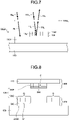
- FIGS. 6 and 7 are schematic views illustrating a method for using the liquid crystal cured layer transfer sticker according to one embodiment of the present invention.
- a laminate 1000 is provided on an adherend 150.
- the laminate 1000 includes a layer 1001 having cholesteric regularity laminated on the adherend 150, the pattern layer 130 adhering to the layer 1001, and a portion 120F of the liquid crystal cured layer laminated on the pattern layer 130.
- the layer 1001 having cholesteric regularity is a layer that can reflect light having a clockwise rotational direction and allow to pass therethrough light having a counterclockwise rotational direction.
- the portion 120F of the liquid crystal cured layer functions as a ⁇ /2 plate.
- the portion 120F of the liquid crystal cured layer is a layer transferred using the liquid crystal cured layer transfer sticker according to the first embodiment.
- a portion of the liquid crystal cured layer may be transferred to the layer 1001 having cholesteric regularity using the liquid crystal cured layer transfer sticker according to another embodiment.
- a circularly polarizing plate 1002 R is overlaid on the laminate 1000, unpolarized light I1 RL is applied, and the layer 1001 included in the laminate 1000 is observed.
- the circularly polarizing plate 1002 R has a function of not allowing to pass therethrough the light having a counterclockwise rotational direction (hereinafter, also referred to as counterclockwise circularly polarized light) and being capable of allowing to pass therethrough the light having a clockwise rotational direction (hereinafter, also referred to as clockwise circularly polarized light).
- clockwise circularly polarized light I2 R passes through the circularly polarizing plate 1002 R to reach the layer 1001.
- the layer 1001 is capable of reflecting the clockwise circularly polarized light as described above, and thus the clockwise circularly polarized light I2 R is reflected by the layer 1001 to become clockwise circularly polarized light I3 R , which reaches the circularly polarizing plate 1002 R .
- the circularly polarizing plate 1002 R allows the clockwise circularly polarized light I3 R to pass therethrough, and clockwise circularly polarized light I4 R is observed.
- unpolarized light I5 RL is applied, and the portion 120F of the liquid crystal cured layer included in the laminate 1000 is observed through the circularly polarizing plate 1002 R .
- clockwise circularly polarized light I6 R passes through the circularly polarizing plate 1002 R to reach the portion 120F.
- the portion 120F functions as a ⁇ /2 plate as described above, and thus the clockwise circularly polarized light I6 R is converted into counterclockwise circularly polarized light I7 L by the portion 120F.
- the layer 1001 passes the counterclockwise circularly polarized light I7 L , and the counterclockwise circularly polarized light I7 L is not observed as reflected light, and thus an image of the portion 120F is not observed.
- a circularly polarizing plate 1002 L is overlaid on the laminate 1000, unpolarized light I8 RL is applied, and the layer 1001 included in the laminate 1000 is observed.
- the circularly polarizing plate 1002 L has a function of not allowing to pass therethrough the clockwise circularly polarized light and being capable of allowing to pass therethrough the counterclockwise circularly polarized light.
- counterclockwise circularly polarized light I9 L passes through the circularly polarizing plate 1002 L to reach the layer 1001.
- the layer 1001 allows the counterclockwise circularly polarized light I9 L to pass therethrough, and the counterclockwise circularly polarized light I9 L is not observed as reflected light.
- the layer 1001 is observed as a dark image.
- unpolarized light I10 RL is applied, and the portion 120F of the liquid crystal cured layer included in the laminate 1000 is observed through the circularly polarizing plate 1002 L .
- counterclockwise circularly polarized light I11 L passes through the circularly polarizing plate 1002 L to reach the portion 120F.
- the counterclockwise circularly polarized light I11 L is converted into clockwise circularly polarized light I12 R by the portion 120F, which reaches the layer 1001.
- the clockwise circularly polarized light I12 R having reached the layer 1001 is reflected by the layer 1001 while maintaining its rotational direction, and then the rotational direction is converted to the opposite direction by the portion 120F to become counterclockwise circularly polarized light I13 L .
- the circularly polarizing plate 1002 L allows the counterclockwise circularly polarized light I13 L to pass therethrough, and counterclockwise circularly polarized light I14 L is observed.
- the liquid crystal cured layer transfer sticker according to one embodiment of the present invention can suitably be used to determine the authenticity of the adherend.
- a liquid crystal cured layer transferred article may include the adherend and the liquid crystal cured layer transferred to the adherend by the liquid crystal cured layer transfer sticker according to any of the embodiments described in the aforementioned item [1. Liquid Crystal Cured Layer Transfer Sticker].
- the liquid crystal cured layer having a pattern is attached to the surface of the adherend via the pattern layer having adhesiveness or the adhesive layer.
- adherend which are not limited to particular adherends, may include paper products such as banknotes and certificates; cloth products such as clothing; leather products such as bags and shoes; and their packaging.
- Peeling strength E between the pattern layer having adhesiveness or the adhesive layer and the aforementioned adherend is usually larger than the peeling strength A between the substrate and the liquid crystal cured layer and is also larger than peeling strength between the liquid crystal cured layer and the pattern layer having adhesiveness or the peeling strength B between the liquid crystal cured layer and the adhesive layer.
- peeling strength E between the pattern layer having adhesiveness or the adhesive layer and the aforementioned adherend is usually larger than the peeling strength A between the substrate and the liquid crystal cured layer and is also larger than peeling strength between the liquid crystal cured layer and the pattern layer having adhesiveness or the peeling strength B between the liquid crystal cured layer and the adhesive layer.
- a method for determining the authenticity of a liquid crystal cured layer transfer sticker according to a third embodiment of the present invention includes Steps (A1) to (A4).
- Step (Al) is performed before Steps (A2) to (A4).
- Step (A4) is performed after Steps (A1) to (A3).
- Step (A3) may be performed after Step (A2), Step (A2) may be performed after Step (A3), or Step (A2) and Step (A3) may be performed simultaneously.
- the method of the third embodiment may include any optional steps in addition to Steps (A1) to (A4).
- the liquid crystal cured layer transfer sticker used in the method of the third embodiment includes the substrate, the liquid crystal cured layer in contact with the substrate through the one face S1, the pattern layer in contact with the partial area F in the other face S2 of the liquid crystal cured layer, and the adhesive layer covering the face S2 of the liquid crystal cured layer and the pattern layer.
- the liquid crystal cured layer is a layer obtained by curing a liquid crystal composition containing a polymerizable liquid crystal compound and has cholesteric regularity, the face S2 of the liquid crystal cured layer is divided by a plurality of incisions, the pattern layer is a layer having peelability, and the substrate is a transparent substrate. Examples and preferred examples of the substrate, the liquid crystal cured layer, the pattern layer having peelability, and the adhesive layer are the same as the examples described in the aforementioned item [1. Liquid Crystal Cured Layer Transfer Sticker].
- Step (A1) the liquid crystal cured layer transfer sticker is attached to the adherend, and the substrate is peeled off from the liquid crystal cured layer transfer sticker attached to the adherend to separate the liquid crystal cured layer transfer sticker into a first member and a second member.
- the first member includes the substrate and the partial area F of the liquid crystal cured layer.
- the second member includes the adhesive layer adhering to the adherend and the area G, which is other than the partial area F of the liquid crystal cured layer.
- FIG. 8 is a schematic view illustrating an example of the members obtained at Step (A1) in the method according to the third embodiment of the present invention.
- this first member 360 includes the substrate 110, the portion 120F including the area F of the liquid crystal cured layer 120 laminated on a partial area of the substrate 110, and the pattern layer 230 laminated on the portion 120F.
- This second member 370 includes the adhesive layer 240 adhering to the adherend 150 through a face 240D and a portion 120G including the area G of the liquid crystal cured layer 120 laminated on the partial area G' of the adhesive layer 240.
- the liquid crystal cured layer 120 is a layer that has cholesteric regularity and can reflect the light having a clockwise rotational direction and allow the light having a counterclockwise rotational direction to pass therethrough.
- the adherend 150 is an absorbing body.
- the pattern layer 230 is a layer having peelability and is constituted as being peelable from at least the adhesive layer 240, and thus by peeling off the substrate 110, the pattern layer 230 peels off from the adhesive layer 240, and the pattern layer 230 is included in the first member 360.
- the pattern layer 230 may peel off from the portion 120F, and the pattern layer 230 may be included in the second member 370.
- Step (A2) the area G of the second member is observed without through the first member to acquire color information C2a of the area G.
- Step (A2) describes Step (A2) with reference to FIG. 9 .
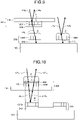
- FIG. 9 is an illustrative view of Steps (A2) and (A3) in the method according to the third embodiment of the present invention.
- unpolarized light L1 RL is applied onto the second member 370 from the portion 120G side.
- the portion 120G of the liquid crystal cured layer can reflect the light having a clockwise rotational direction.
- polarized light L2 R having a clockwise rotational direction included in the unpolarized light L1 RL applied onto the portion 120G is reflected by the portion 120G.
- the portion 120G of the liquid crystal cured layer can allow the light having a counterclockwise rotational direction to pass therethrough.
- polarized light L3 L having a counterclockwise rotational direction included in the unpolarized light L1 RL passes through the portion 120G.
- the area G is observed as an image having the color information C2a (chromaticity, saturation, and brightness, for example) that is different from that of the surrounding area of the area G.
- C2a chromaticity, saturation, and brightness, for example
- the first member is overlaid on the second member such that at least a portion of the area F overlaps the area G when viewed in the thickness direction with the substrate set as an observation side, and the area G is observed from the substrate side of the first member to obtain color information C3a of the area G.
- Step (A3) with reference to FIG. 9 .
- the first member 360 is overlaid on the second member 370 with the substrate 110 set as an observation side.
- an area f which is a portion of the area F of the portion 120F, is made to overlap the area G when viewed in the thickness direction of the first member 360. It is preferable to place the first member 360 such that the pattern layer 230 of the first member 360 and the portion 120G of the second member 370 are in contact with each other.
- unpolarized light L4 RL is applied onto the first member 360 and the second member 370 from the substrate 110 side.
- the portion 120F of the first member 360 can allow the light having a counterclockwise rotational direction to pass therethrough.
- polarized light L5 L having a counterclockwise rotational direction included in the unpolarized light L4 RL applied onto the portion 120F passes through the portion 120F.
- the portion 120G of the second member 370 can also allwo the light having a counterclockwise rotational direction to pass therethrough.
- the polarized light L5 L passes through the portion 120G.
- polarized light L6 R having a clockwise rotational direction included in the unpolarized light L4 RL applied onto the portion 120F is reflected by the portion 120F and does not reach the portion 120G.
- reflected light by the portion 120G is not observed.
- the color information C3a of the area G does not include information on the reflected light by the portion 120G, and the color information C3a observed from the area G is the same as or scarcely different from the color information of the surrounding area of the area G, making it hard for the naked eye to recognize the image of the area G.
- Step (A4) the color information C2a of the area G acquired at Step (A2) and the color information C3a of the area G acquired at Step (A3) are compared with each other; if there is a difference between the color information C2a and the color information C3a, it is determined that the liquid crystal cured layer transfer sticker is authentic, whereas if there is no difference between the color information C2a and the color information C3a, it is determined that the liquid crystal cured layer transfer sticker is not authentic.
- the color information C2a obtained at Step (A2) includes the information on the reflected light by the portion 120G, whereas the color information C3a obtained at Step (A3) does not include the information on the reflected light of the portion 120G.
- the color information C2a and the color information C3a there arises a difference between the color information C2a and the color information C3a.
- the liquid crystal cured layer transfer sticker does not have the configuration according to one embodiment of the present invention, and it is determined that the liquid crystal cured layer transfer sticker is not authentic.
- a method according to a fourth embodiment of the present invention is a method for determining the authenticity of a liquid crystal cured layer transfer sticker when the substrate functions as a ⁇ /2 plate and the pattern layer is a layer having peelability.
- the method for determining the authenticity of a liquid crystal cured layer transfer sticker includes Step (A1), Step (A3), Step (A5), and Step (A6).
- Step (A1) is performed before Step (A3), Step (A5), and Step (A6).
- Step (A6) is performed after Step (A1), Step (A3), and Step (A5).
- Step (A5) may be performed after Step (A3) or Step (A3) may be performed after Step (A5).
- Step (A3) and Step (A5) are usually not performed simultaneously.
- the liquid crystal cured layer transfer sticker used in the method according to the present embodiment includes the substrate, the liquid crystal cured layer in contact with the substrate through the one face S1, the pattern layer in contact with the partial area F in the other face S2 of the liquid crystal cured layer, and the adhesive layer covering the face S2 of the liquid crystal cured layer and the pattern layer.
- the liquid crystal cured layer is a layer obtained by curing a liquid crystal composition containing a polymerizable liquid crystal compound and has cholesteric regularity, the face S2 of the liquid crystal cured layer is divided by a plurality of incisions, the pattern layer is a layer having peelability, the substrate is a transparent substrate, and the retardation at a measurement wavelength of 550 nm of the substrate in the in-plane direction is (550n/2 - 50) nm or more and (550n/2 + 50) nm or less, n being an odd number of 1 or more.
- Examples and preferred examples of the substrate, the liquid crystal cured layer, the pattern layer having peelability, and the adhesive layer are the same as the examples described in the aforementioned item [1. Liquid Crystal Cured Layer Transfer Sticker].
- Step (A1) in the same manner as in Step (A1) according to the third embodiment, the liquid crystal cured layer transfer sticker is attached to the adherend, and the transparent substrate is peeled off from the liquid crystal cured layer transfer sticker attached to the adherend to separate the liquid crystal cured layer transfer sticker into the first member and the second member.
- Step (A1) according to the fourth embodiment is the same as Step (A1) according to the third embodiment except that the liquid crystal cured layer transfer sticker is a specific liquid crystal cured layer transfer sticker in which the substrate functions as a ⁇ /2 plate.
- Step (A3) in the same manner as in Step (A3) according to the third embodiment, the first member is overlaid on the second member such that at least a portion of the area F overlaps the area G when viewed in the thickness direction with the substrate set as an observation side, and the area G is observed from the substrate side of the first member to obtain the color information C3a of the area G.
- Step (A3) according to the fourth embodiment is the same as Step (A3) according to the third embodiment except that the substrate is a specific substrate functioning as a ⁇ /2 plate. The substrate functions as a ⁇ /2 plate. Usually, when unpolarized light is applied onto the substrate, the light having passed through the substrate is unpolarized light.
- the color information C3a of the area G obtained at Step (A3) according to the fourth embodiment does not include the information on the reflected light by the portion including the area G of the liquid crystal cured layer.
- the color information C3a observed from the area G is the same as or scarcely different from the color information of the surrounding area of the area G, making it hard for the naked eye to recognize the image of the area G.
- the first member is overlaid on the second member such that at least a portion of the area F overlaps the area G when viewed in the thickness direction with the liquid crystal cured layer set as an observation side, and the area G is observed from the liquid crystal cured layer side of the first member to obtain color information C5a of the area G.
- Step (A5) with reference to FIG. 10 .
- the first member 360 is overlaid on the second member 370 with the portion 120F, which is a portion of the liquid crystal cured layer, set as an observation side.
- the area f which is a portion of the area F of the portion 120F, is made to overlap the area G of the portion 120G, which is a portion of the liquid crystal cured layer, when viewed in the thickness direction of the first member 360. It is preferable to place the first member 360 such that the substrate 110 of the first member 360 and the portion 120G of the second member 370 are in contact with each other.
- unpolarized light L7 RL is applied onto the first member 360 and the second member 370 from the portion 120F side (specifically, the pattern layer 230 side).
- the portion 120F of the liquid crystal cured layer can allow the light having a counterclockwise rotational direction to pass therethrough as described in the method of the third embodiment.
- polarized light L8 L having a counterclockwise rotational direction passes through the portion 120F.
- the polarized light L8 L having passed through the portion 120F then passes through the substrate 110.
- the substrate 110 functions as a ⁇ /2 plate.
- the polarized light L8 L is given a phase difference when passing through the substrate 110 to become polarized light L9 R having a clockwise rotational direction, which is opposite to that of the polarized light L8 L .
- the portion 120G of the second member 370 is capable of reflecting the light having a clockwise rotational direction.
- the polarized light L9 R is reflected by the portion 120G to become polarized light L10 R .
- the polarized light L10 R then passes through the substrate 110.
- the polarized light L10 R is given a phase difference when passing through the substrate 110 to become polarized light L11 L having a counterclockwise rotational direction, which is opposite to that of the polarized light L10 R .
- the polarized light L11 L passes through the portion 120F, which is capable of allowing the light having a counterclockwise rotational direction to pass therethrough.
- the area G is observed as an image having the color information C5a different from that of the surrounding area of the area G.
- the color information C3a of the area G acquired at Step (A3) and the color information C5a of the area G acquired at Step (A5) are compared with each other; if there is a difference between the color information C3a and the color information C5a, it is determined that the liquid crystal cured layer transfer sticker is authentic, whereas if there is no difference between the color information C3a and the color information C5a, it is determined that the liquid crystal cured layer transfer sticker is not authentic.
- the color information C3a obtained at Step (A3) does not include the information on the reflected light of the portion 120G
- the color information C5a obtained at Step (A5) includes the information on the reflected light of the portion 120G.
- the color information C3a and the color information C5a there arises a difference between the color information C3a and the color information C5a.
- the liquid crystal cured layer transfer sticker does not have the configuration according to one embodiment of the present invention, and it is determined that the liquid crystal cured layer transfer sticker is not authentic.
- the method according to the fourth embodiment may include any optional steps in addition to Step (A1), Step (A3), Step (A5), and Step (A6).
- the method according to the fourth embodiment may include Step (A2) and Step (A4) in the method according to the third embodiment, for example.
- Step (A2) and Step (A4) in addition to Step (A1), Step (A3), Step (A5), and Step (A6), authenticity determination for the liquid crystal cured layer transfer sticker can be performed more surely.
- a method for determining the authenticity of a liquid crystal cured layer transfer sticker according to a fifth embodiment of the present invention includes Steps (B1) to (B4).
- Step (Bl) is performed before Steps (B2) to (B4).
- Step (B4) is performed after Steps (B1) to (B3).
- Step (B3) may be performed after Step (B2), Step (B2) may be performed after Step (B3), or Step (B2) and Step (B3) may be performed simultaneously.
- the method of the fifth embodiment may include any optional steps in addition to Steps (B1) to (B4).
- the liquid crystal cured layer transfer sticker used in the method of the fifth embodiment includes the substrate, the liquid crystal cured layer in contact with the substrate through the one face S1, and the pattern layer in contact with the partial area F in the other face S2 of the liquid crystal cured layer.
- the liquid crystal cured layer is a layer obtained by curing a liquid crystal composition containing a polymerizable liquid crystal compound and has cholesteric regularity, the face S2 of the liquid crystal cured layer is divided by a plurality of incisions, the pattern layer is a layer having adhesiveness, and the substrate is a transparent substrate. Examples and preferred examples of the substrate, the liquid crystal cured layer, and the pattern layer having adhesiveness are the same as the examples described in the aforementioned item [1. Liquid Crystal Cured Layer Transfer Sticker].
- the liquid crystal cured layer transfer sticker is attached to the adherend, and the substrate is peeled off from the liquid crystal cured layer transfer sticker attached to the adherend to separate the liquid crystal cured layer transfer sticker into a first member and a second member.
- the first member includes the substrate and the area G, which is other than the partial area F of the liquid crystal cured layer.
- the second member includes the pattern layer adhering to the adherend and the partial area F of the liquid crystal cured layer.
- FIG. 11 is a schematic view illustrating an example of the members obtained at Step (B1) in the method according to the fifth embodiment of the present invention.
- This first member 560 includes the substrate 110 and the portion 120G including the area G of the liquid crystal cured layer 120 laminated on a partial area of the substrate 110.
- This second member 570 includes the portion 120F including the area F of the liquid crystal cured layer 120 and the pattern layer 130 causing the portion 120F and the adherend 150 to adhere to each other.
- the liquid crystal cured layer 120 is a layer that has cholesteric regularity and is capable of reflecting the light having a clockwise rotational direction and of allowing the light having a counterclockwise rotational direction to pass therethrough.
- the adherend 150 is an absorbing body.
- the pattern layer 130 is a layer having adhesiveness and is in contact with the partial area F of the liquid crystal cured layer 120, and thus the portion 120F including the area F of the liquid crystal cured layer 120 adheres to the adherend 150 via the pattern layer 130.
- the pattern layer 130 is not in contact with the portion 120G including the area G, which is other than the area F of the liquid crystal cured layer 120, and thus the portion 120G does not adhere to the adherend 150.
- Step (B2) the area F of the second member is observed without intervention of the first member to acquire color information C2b of the area F.
- Step (B2) describes Step (B2) with reference to FIG. 12 .
- FIG. 12 is an illustrative view of Step (B2) in the method according to the fifth embodiment of the present invention.
- unpolarized light L101 RL is applied onto the second member 570 from the portion 120F side.
- the portion 120F of the liquid crystal cured layer is capable of reflecting the light having a clockwise rotational direction.
- polarized light L102 R having a clockwise rotational direction included in the unpolarized light L101 RL applied onto the portion 120F is reflected by the portion 120F.
- the portion 120F of the liquid crystal cured layer is capable of allowing the light having a counterclockwise rotational direction to pass therethrough.
- polarized light L103 L having a counterclockwise rotational direction included in the unpolarized light L101 RL passes through the portion 120F.
- the area F is observed as an image having the color information C2b (chromaticity, saturation, and brightness, for example) different from that of the surrounding area of the area F.
- C2b chromaticity, saturation, and brightness, for example
- the first member is overlaid on the second member such that at least a portion of the area G overlaps the area F when viewed in the thickness direction with the substrate set as an observation side, and the area F is observed from the substrate side of the first member to obtain color information C3b of the area F.
- Step (B3) with reference to FIG. 13 .
- FIG. 13 is an illustrative view of Step (B3) in the method according to the fifth embodiment of the present invention.
- the first member 560 is overlaid on the second member 570 with the substrate 110 set as an observation side.
- the substrate 110 set as an observation side.
- at least a portion of the area G is made to overlap the area F when viewed in the thickness direction of the first member 560. It is preferable to place the first member 560 such that the portion 120G of the liquid crystal cured layer included in the first member 560 and the portion 120F of the second member 570 are in contact with each other.
- unpolarized light L104 RL is applied onto the first member 560 and the second member 570 from the substrate 110 side.
- the portion 120G of the first member 560 is capable of allowing the light having a counterclockwise rotational direction to pass therethrough.
- polarized light L105 L having a counterclockwise rotational direction included in the unpolarized light L104 RL applied onto the portion 120G passes through the portion 120G.
- polarized light L106 R having a clockwise rotational direction included in the unpolarized light L104 RL applied onto the portion 120G is reflected by the portion 120G and does not reach the portion 120F.
- reflected light by the portion 120F is not observed.
- the color information C3b of the area F does not include information on the reflected light by the portion 120F, and the color information C3b observed from the area F is the same as or scarcely different from the color information of the surrounding area of the area F, making it hard for the naked eye to recognize the image of the area F.
- the color information C2b of the area F acquired at Step (B2) and the color information C3b of the area F acquired at Step (B3) are compared with each other; if there is a difference between the color information C2b and the color information C3b, it is determined that the liquid crystal cured layer transfer sticker is authentic, whereas if there is no difference between the color information C2b and the color information C3b, it is determined that the liquid crystal cured layer transfer sticker is not authentic.
- the color information C2b obtained at Step (B2) includes the information on the reflected light by the portion 120F, whereas the color information C3b obtained at Step (B3) does not include the information on the reflected light of the portion 120F.
- the color information C2b and the color information C3b there arises a difference between the color information C2b and the color information C3b.
- the liquid crystal cured layer transfer sticker does not have the configuration according to one embodiment of the present invention, and it is determined that the liquid crystal cured layer transfer sticker is not authentic.
- a method according to a sixth embodiment of the present invention is a method for determining the authenticity of a liquid crystal cured layer transfer sticker when the substrate functions as a ⁇ /2 plate and the pattern layer is a layer having adhesiveness.
- the method for determining the authenticity of a liquid crystal cured layer transfer sticker includes Step (B1), Step (B3), Step (B5), and Step (B6).
- Step (B1) is performed before Step (B3), Step (B5), and Step (B6).
- Step (B6) is performed after Step (B1), Step (B3), and Step (B5).
- Step (B5) may be performed after Step (B3) or Step (B3) may be performed after Step (B5).
- Step (B3) and Step (B5) are usually not performed simultaneously.
- the liquid crystal cured layer transfer sticker used in the method according to the present embodiment includes the substrate, the liquid crystal cured layer in contact with the substrate through the one face S1, and the pattern layer in contact with the partial area F in the other face S2 of the liquid crystal cured layer.
- the liquid crystal cured layer is a layer obtained by curing a liquid crystal composition containing a polymerizable liquid crystal compound and has cholesteric regularity, the face S2 of the liquid crystal cured layer is divided by a plurality of incisions, the pattern layer is a layer having adhesiveness, the substrate is a transparent substrate, and the retardation at a measurement wavelength of 550 nm of the substrate in the in-plane direction is (550n/2 - 50) nm or more and (550n/2 + 50) nm or less, n being an odd number of 1 or more.
- Examples and preferred examples of the substrate, the liquid crystal cured layer, and the pattern layer having adhesiveness are the same as the examples described in the aforementioned item [1. Liquid Crystal Cu
- Step (B1) in the same manner as in Step (B1) according to the fifth embodiment, the liquid crystal cured layer transfer sticker is attached to the adherend, and the transparent substrate is peeled off from the liquid crystal cured layer transfer sticker attached to the adherend to separate the liquid crystal cured layer transfer sticker into the first member and the second member.
- Step (B1) according to the sixth embodiment is the same as Step (B1) according to the fifth embodiment except that the liquid crystal cured layer transfer sticker is a specific liquid crystal cured layer transfer sticker in which the substrate functions as a ⁇ /2 plate.
- Step (B3) the first member is overlaid on the second member such that at least a portion of the area G overlaps the area F when viewed in the thickness direction with the substrate set as an observation side, and the area F is observed from the substrate side of the first member to obtain the color information C3b of the area F.
- Step (B3) according to the sixth embodiment is the same as Step (B3) according to the fifth embodiment except that the substrate is a specific substrate functioning as a ⁇ /2 plate.
- the substrate functions as a ⁇ /2 plate.
- the light having passed through the substrate is unpolarized light.
- the color information C3b of the area F obtained at Step (B3) according to the sixth embodiment does not include the information on the reflected light by the portion including the area F of the liquid crystal cured layer.
- the color information C3b observed from the area F is the same as or scarcely different from the color information of the surrounding area of the area F, making it hard for the naked eye to recognize the image of the area F.
- the first member is overlaid on the second member such that at least a portion of the area G overlaps the area F when viewed in the thickness direction with the liquid crystal cured layer set as an observation side, and the area F is observed from the liquid crystal cured layer side of the first member to obtain color information C5b of the area F.
- Step (B5) with reference to FIG. 14 .
- FIG. 14 is an illustrative view of Step (B5) in the method according to the sixth embodiment of the present invention.
- the first member 560 is overlaid on the second member 570 with the portion 120G, which is a portion of the liquid crystal cured layer, set as an observation side.
- the portion 120G which is a portion of the liquid crystal cured layer, set as an observation side.
- at least part of the area G is made to overlap the area F when viewed in the thickness direction of the first member 560. It is preferable to place the first member 560 such that the substrate 110 of the first member 560 and the portion 120F of the second member 570 are in contact with each other.
- unpolarized light L107 RL is applied onto the first member 560 and the second member 570 from the portion 120G side.
- the portion 120G of the liquid crystal cured layer is capable of allowing the light having a counterclockwise rotational direction to pass therethrough, as with described in the method of the fifth embodiment.
- polarized light L108 L having a counterclockwise rotational direction passes through the portion 120G.
- the polarized light L108 L having passed through the portion 120G then passes through the substrate 110.
- the substrate 110 functions as a ⁇ /2 plate.
- the polarized light L108 L is given a phase difference when passing through the substrate 110 to become polarized light L109 R having a clockwise rotational direction, which is opposite to that of the polarized light L108 L .
- the portion 120F of the second member 570 is capable of reflecting the light having a clockwise rotational direction.
- the polarized light L109 R is reflected by the portion 120F to become polarized light L110 R .
- the polarized light L110 R then passes through the substrate 110.
- the polarized light L110 R is given a phase difference when passing through the substrate 110 to become polarized light L111 L having a counterclockwise rotational direction, which is opposite to that of the polarized light L110R.
- the polarized light L111 L passes through the portion 120G, which is capable of allowing the light having a counterclockwise rotational direction to pass therethrough.
- the area F is observed as an image having the color information C5b different from that of the surrounding area of the area F.
- the color information C3b of the area F acquired at Step (B3) and the color information C5b of the area F acquired at Step (B5) are compared with each other; if there is a difference between the color information C3b and the color information C5b, it is determined that the liquid crystal cured layer transfer sticker is authentic, whereas if there is no difference between the color information C3b and the color information C5b, it is determined that the liquid crystal cured layer transfer sticker is not authentic.
- the color information C3b obtained at Step (B3) does not include the information on the reflected light of the portion 120F
- the color information C5b obtained at Step (B5) includes the information on the reflected light of the portion 120F.
- the color information C3b and the color information C5b there arises a difference between the color information C3b and the color information C5b.
- the liquid crystal cured layer transfer sticker does not have the configuration according to one embodiment of the present invention, and it is determined that the liquid crystal cured layer transfer sticker is not authentic.
- the method according to the sixth embodiment may include any optional steps in addition to Step (B1), Step (B3), Step (B5), and Step (B6).
- the method according to the sixth embodiment may include Step (B2) and Step (B4) in the method according to the fifth embodiment, for example.
- Step (B2) and Step (B4) in addition to Step (B1), Step (B3), Step (B5), and Step (B6), authenticity determination for the liquid crystal cured layer transfer sticker can be performed more surely.
- Example Group A liquid crystal cured layer transfer stickers including a layer configuration of (the transparent substrate)/(the cholesteric liquid crystal cured layer)/(the pattern layer having peelability)/(the adhesive layer) were produced, and a liquid crystal cured layer thereof is transferred to an adherend. Then the clarity of a transferred character pattern was evaluated.
- a resin containing an alicyclic structure-containing polymer (“ZEONOR” manufactured by ZEON CORPORATION) was fed into a feeder of a single-screw extruder (manufactured by OCS) and was melt extruded to obtain a pre-stretch film with a thickness of 200 ⁇ m.
- the resulting pre-stretch film was uniaxially stretched using a biaxial stretching test apparatus (manufactured by Toyo Seiki Seisaku-sho, Ltd.) to obtain a transparent substrate with a thickness of 142 ⁇ m.
- the conditions for uniaxial stretching are as follows:
- photopolymerization initiator (parts) 0.9 surfactant (parts) 0.03 cyclopentanone (parts) 70
- a surface of the transparent substrate was subjected to rubbing treatment.
- the liquid crystal composition was applied onto the face of the transparent substrate that had been subjected to the rubbing treatment using a bar coater to form a layer of the liquid crystal composition.
- the layer of the liquid crystal composition was subjected to orientation treatment that was heating at 120°C for 4 minutes.
- application of weak ultraviolet rays of 30 mJ/m 2 or less and heating treatment at 100°C were repeated a plurality of times.
- ultraviolet rays of 800 mJ/cm 2 were applied onto the layer of the liquid crystal composition to cure the layer of the liquid crystal composition.
- a cholesteric liquid crystal cured layer was obtained as a liquid crystal cured layer.
- the thickness of the obtained cholesteric liquid crystal cured layer is shown in Table 2.
- the peeling strength between the cholesteric liquid crystal cured layer and the transparent substrate was measured, and it was 0.4 N/25 mm.
- the peeling strength was measured by the method of the 180° peeling test, in which one layer is peeled off in a 180° direction using "Digital Force Gauge ZP-50" manufactured by Imada Co., Ltd.
- a metal mold was pressed against the cholesteric liquid crystal cured layer (the liquid crystal cured layer) side of the obtained multilayer film using a small heat pressing machine to make a plurality of incisions in the cholesteric liquid crystal cured layer.
- a small heat pressing machine "H300-10D" manufactured by As One Corporation was used.
- the metal mold was not heated, and incising was performed at room temperature.
- a metal mold having a plurality of linear protrusions with an interval between adjacent ridges of 50 ⁇ m was used. The plurality of the protrusions are parallel to each other.
- the metal mold was pressed against the multilayer film such that the direction of the protrusions was parallel to the direction of one edge of the multilayer film, and then the metal mold was pressed against the multilayer film such that the direction of the protrusions was orthogonal to the direction of the one edge of the multilayer film.
- the pressing pressure of the metal mold was set to 0.5 MPa.
- the depth of the incisions was measured as follows.
- the multilayer film was sliced with a microtome to obtain a sample piece enabling a section of the multilayer film in the thickness direction to be observed.
- the obtained sample piece was observed under a scanning electron microscope (JEOL/JSM-7401F manufactured by JEOL Ltd.) to measure the depth of the incisions made in the cholesteric liquid crystal cured layer of the multilayer film.
- the pressing pressure of the metal mold, the depth of the incisions, the length of one edge of the grid (the pitch of the incisions), and the value of (the depth of the incisions)/(the thickness of the cholesteric liquid crystal cured layer) are shown in Table 2.
- a character pattern was printed using a gravure printer to form a pattern layer.
- ink "KNS-3051” manufactured by Shin-Etsu Chemical Co., Ltd. was used.
- the thickness of the pattern layer was about 1 ⁇ m.
- a pressure-sensitive adhesive layer with a peelable sheet (a layer containing an acrylic adhesive, "NE-tak PET-21WF” manufactured by Nichiei Kaken) was prepared.
- the pressure-sensitive adhesive layer as an adhesive layer was attached to the side formed with the pattern layer of the multilayer film formed with the pattern layer.
- the peelable sheet of the pressure-sensitive adhesive layer was peeled off, and the multilayer film (the liquid crystal cured layer transfer sticker) was attached to a black acrylic plate. Then, the transparent substrate was peeled off from the multilayer film to break the multilayer film into a member (the first member) including the transparent substrate and a member (the second member) remained attached to the acrylic plate. A partial area of the cholesteric liquid crystal cured layer remained on the transparent substrate of the first member in the same pattern as the printed character-patterned pattern layer. The pattern layer adhered to the pressure-sensitive adhesive layer. A partial area of the cholesteric liquid crystal cured layer remained on the pressure-sensitive adhesive layer of the second member.
- the area of the cholesteric liquid crystal cured layer that remained on the second member had the same shape as that of an area of the cholesteric liquid crystal cured layer on which the character pattern was not printed. From the structures of the first member and the second member obtained, it can be seen that the peeling strength A between the transparent substrate and the cholesteric liquid crystal cured layer and the peeling strength B between the cholesteric liquid crystal cured layer and the pressure-sensitive adhesive layer are in a relation of A ⁇ B.
- the multilayer film (the liquid crystal cured layer transfer sticker) according to the present Example satisfies the aforementioned conditions (i) and (ii) .
- the first member was overlaid on the second member such that the transparent substrate side of the first member was a visual recognition side.
- the character pattern of the first member was made to overlap a portion of the cholesteric liquid crystal cured layer included in the second member.
- the outline of the area of the cholesteric liquid crystal cured layer included in the first member and the outline of the area of the cholesteric liquid crystal cured layer included in the second member were observed with the naked eye, and the clarity of the outlines was evaluated according to the following criteria.
- Multilayer films (liquid crystal cured layer transfer stickers) were obtained and evaluated in the same manner as in Example A1 except that the following items were changed.
- Example A4 to A15 the application conditions of the liquid crystal composition were adjusted so as to obtain the cholesteric liquid crystal cured layer of the thickness listed in Table 2 in (Production of Cholesteric Liquid Crystal Cured Layer (Liquid Crystal Cured Layer)).
- the first member was overlaid on the second member such that the transparent substrate side of the first member was a visual recognition side.
- the character pattern of the first member was made to overlap a portion of the cholesteric liquid crystal cured layer included in the second member.
- Multilayer films (liquid crystal cured layer transfer stickers) were obtained and evaluated in the same manner as in Example A1 except that the following items were changed.
- Comparative Examples CA2 and CA3 the application conditions of the liquid crystal composition were adjusted so as to obtain the cholesteric liquid crystal cured layer of the thickness listed in Table 2 in (Production of Cholesteric Liquid Crystal Cured Layer (Liquid Crystal Cured Layer)).
- Example Group A The results of Example Group A were shown in Table 2.
- Example Group B liquid crystal cured layer transfer stickers including a layer configuration of (the transparent substrate)/(the cholesteric liquid crystal cured layer)/(the pattern layer having adhesiveness) were produced, and the clarity of a transferred character pattern was evaluated.
- Example A1 In the same manner as in Example A1, a multilayer film having a layer configuration of (the transparent substrate)/(the cholesteric liquid crystal cured layer) was obtained. Then, in the same manner as in Example A1, incising was performed into the liquid crystal cured layer of the obtained multilayer film to obtain a multilayer film with the cholesteric liquid crystal cured layer subjected to incising. The depth of the incisions was measured in the same manner as in Example A1. The pressing pressure of the metal mold, the depth of the incisions, the length of one edge of the grid (the pitch of the incisions), and the value of (the depth of the incisions)/(the thickness of the cholesteric liquid crystal cured layer) were shown in Table 3.
- a character pattern was printed using a screen printer to form a pattern layer having adhesiveness.
- ink a water-based pressure-sensitive adhesive "1549" for screen printing manufactured by ThreeBond Co., Ltd was used.
- the thickness of the pattern layer was 10 ⁇ m.
- the multilayer film (the liquid crystal cured layer transfer sticker) formed with the pattern layer was attached to a black acrylic plate.
- the face of the multilayer film formed with the pattern layer was made in close contact with the acrylic plate.
- the transparent substrate was peeled off from the multilayer film to break the multilayer film into a member (the first member) including the transparent substrate and a member (the second member) remained attached to the acrylic plate.
- the second member including the printed character-patterned pattern layer and a partial area of the liquid crystal cured layer having the same pattern as that of the pattern layer attached to the acrylic plate.
- a partial area of the cholesteric liquid crystal cured layer remained on the transparent substrate.
- the area of the cholesteric liquid crystal cured layer that remained on the transparent substrate had the same shape as that of an area of the cholesteric liquid crystal cured layer on which the character pattern was not printed.
- the outline of the area of the cholesteric liquid crystal cured layer included in the first member and the outline of the area of the cholesteric liquid crystal cured layer included in the second member were observed in the same manner as in Example A1, and the clarity of the outlines was evaluated according to the same criteria.
- the first member was overlaid on the character pattern of the second member such that the transparent substrate side was a visual recognition side.
- a portion of the cholesteric liquid crystal cured layer included in the first member was made to overlap the character pattern of the second member.
- Multilayer films (liquid crystal cured layer transfer stickers) were obtained and evaluated in the same manner as in Example B1 except that the following items were changed.
- Example B4 to B15 the application conditions of the liquid crystal composition were adjusted so as to obtain the cholesteric liquid crystal cured layer of the thickness listed in Table 3 in (Production of Cholesteric Liquid Crystal Cured Layer (Liquid Crystal Cured Layer)).
- the first member was overlaid on the character pattern of the second member such that the transparent substrate side was a visual recognition side.
- a portion of the cholesteric liquid crystal cured layer included in the first member was made to overlap the character pattern.
- Multilayer films (liquid crystal cured layer transfer stickers) were obtained and evaluated in the same manner as in Example B1 except that the following items were changed.
- Example Group B The results of Example Group B are shown in Table 3.
- liquid crystal cured layer transfer stickers including a layer configuration of (the transparent substrate)/(the liquid crystal cured layer having a phase difference in the in-plane direction)/(the pattern layer having peelability)/(the adhesive layer) were produced, and a liquid crystal cured layer thereof is transferred to an adherend. Then the clarity of a transferred character pattern was evaluated.
- a transparent substrate was produced in the same manner as in (Production of Transparent Substrate) of Example A1.
- the transparent substrate functioned as a ⁇ /2 plate as with the transparent substrate produced in Example A1.
- a photopolymerizable liquid crystal compound (“LC242” manufactured by BASF), a photopolymerizable non-liquid crystal compound represented by Formula (X2) described above, a photopolymerization initiator ("Irgacure OXEO2” manufactured by Ciba Japan K.K.), a surfactant (“Ftargent 209F” manufactured by Neos Company Limited), and cyclopentanone as a solvent were mixed in the amounts listed in Table 4 shown below to prepare a liquid crystal composition.
- a surface of the transparent substrate was subjected to rubbing treatment.
- the liquid crystal composition was applied onto the face of the transparent substrate that had been subjected to the rubbing treatment using a bar coater to form a layer of the liquid crystal composition.
- the layer of the liquid crystal composition was subjected to orientation treatment that was heating at 120°C for 4 minutes.
- Ultraviolet rays of 800 mJ/cm 2 were applied onto the layer of the liquid crystal composition for 30 seconds to cure the layer of the liquid crystal composition. Thereby a liquid crystal cured layer was obtained.
- the thickness of the obtained liquid crystal cured layer was shown in Table 5.
- the peeling strength between the liquid crystal cured layer and the transparent substrate was measured in the same manner as in Example A1, and it was 0.4 N/25 mm.
- Example A1 A plurality of incisions were made in the liquid crystal cured layer of the obtained multilayer film in the same manner as in (Incising into Liquid Crystal Cured Layer) of Example A1. The depth of the incisions made in the liquid crystal cured layer was measured in the same manner as in Example A1.
- the pressing pressure of the metal mold, the depth of the incisions, the length of one edge of the grid (the pitch of the incisions), and the value of (the depth of the incisions)/(the thickness of the liquid crystal cured layer) are shown in Table 5.
- a pattern layer having peelability was formed on the liquid crystal cured layer of the multilayer film that had been subjected to incising in the same manner as in Example A1.
- the thickness of the pattern layer was about 1 ⁇ m.
- a pressure-sensitive adhesive layer was attached to the multilayer film in the same manner as in Example A1.
- the liquid crystal cured layer transfer sticker was evaluated in the same manner as in Example A1.
- a partial area of the liquid crystal cured layer remained on the transparent substrate of the first member in the same pattern as the printed character-patterned pattern layer.
- the pattern layer adhered to a partial area of the liquid crystal cured layer.
- a partial area of the liquid crystal cured layer remained on the pressure-sensitive adhesive layer of the second member.
- the area of the liquid crystal cured layer that remained on the second member had the same shape as that of an area of the liquid crystal cured layer on which the character pattern was not printed.
- the peeling strength A between the transparent substrate and the liquid crystal cured layer and the peeling strength B between the liquid crystal cured layer and the pressure-sensitive adhesive layer are in a relation of A ⁇ B.
- the multilayer film (the liquid crystal cured layer transfer sticker) according to the present Example satisfies the aforementioned conditions (i) and (ii) .
- Multilayer films (liquid crystal cured layer transfer stickers) were obtained and evaluated in the same manner as in Example C1 except that the following items were changed.
- the application conditions of the liquid crystal composition were adjusted so as to obtain the liquid crystal cured layer of the thickness listed in Table 5 in (Production of Liquid Crystal Cured Layer).
- Example C3 the pressing pressure of the metal mold was set as listed in Table 5.
- Multilayer films (liquid crystal cured layer transfer stickers) were obtained and evaluated in the same manner as in Example C1 except that the following items were changed.
- Comparative Example CC2 the application conditions of the liquid crystal composition were adjusted so as to obtain the liquid crystal cured layer of the thickness listed in Table 5 in (Production of Liquid Crystal Cured Layer).
- Example Group C The results of Example Group C are shown in Table 5.
- Table 5 d ( ⁇ m) pressi ng pressu re (MPa) depth of incisi ons ( ⁇ m) incision size (pitch) ( ⁇ m) outline clarity depth of incision s/d Comp. Ex. CC1 1 0 0 - Bad - Ex. C1 1 0.5 1 50 Good 1.0 Comp. Ex. CC2 2 0 0 - Bad - Ex. C2 2 0.5 1 50 Accepta ble 0.5 Ex. C3 2 1 1.5 50 Good 0.8
- Example group D liquid crystal cured layer transfer stickers including a layer configuration of (the transparent substrate)/(the liquid crystal cured layer having a phase difference in the in-plane direction)/(the pattern layer having adhesiveness) were produced, and the clarity of a transferred character pattern was evaluated.
- Example C1 In the same manner as in Example C1, a multilayer film having a layer configuration of (the transparent substrate)/(the liquid crystal cured layer) was obtained, and a plurality of incisions were made in the liquid crystal cured layer. The depth of the incisions made in the liquid crystal cured layer was measured in the same manner as in Example A1. The retardation of the liquid crystal cured layer in the in-plane direction was 140 nm at a measurement wavelength of 550 nm as with the liquid crystal cured layer in Example C1, and thus the liquid crystal cured layer can function as a ⁇ /4 plate.
- the pressing pressure of the metal mold, the depth of the incisions, the length of one edge of the grid (the pitch of the incisions), and the value of (the depth of the incisions)/(the thickness of the liquid crystal cured layer) are shown in Table 6.
- a pattern layer having adhesiveness was formed in the same manner as in Example B1.
- the thickness of the pattern layer was 10 ⁇ m.
- the multilayer film (the liquid crystal cured layer transfer sticker) formed with the pattern layer was evaluated in the same manner as in Example B1.
- Multilayer films (liquid crystal cured layer transfer stickers) were obtained and evaluated in the same manner as in Example D1 except that the following items were changed.
- the application conditions of the liquid crystal composition were adjusted so as to obtain the liquid crystal cured layer of the thickness listed in Table 6 in (Production of Liquid Crystal Cured Layer).
- Example D3 the pressing pressure of the metal mold was set as listed in Table 6.
- the retardation of the liquid crystal cured layer in the in-plane direction was 280 nm at a measurement wavelength of 550 nm, and thus the liquid crystal cured layer can function as a ⁇ /2 plate.
- Example D2 When the retardation of the liquid crystal cured layer obtained in Example D2 in the in-plane direction was measured in the same manner as in Example C1, it was 280 nm, revealing that the liquid crystal cured layer functioned as a ⁇ /2 plate.
- Multilayer films (liquid crystal cured layer transfer stickers) were obtained and evaluated in the same manner as in Example D1 except that the following items were changed.
- Comparative Example CD2 the application conditions of the liquid crystal composition were adjusted so as to obtain the liquid crystal cured layer of the thickness listed in Table 6 in (Production of Liquid Crystal Cured Layer).
- Example Group D The results of Example Group D are shown in Table 6.
- Table 6 d ( ⁇ m) pressi ng pressu re (MPa) depth of incisi ons ( ⁇ m) Incision size (pitch) ( ⁇ m) Outline clarity depth of incision s/d Comp. Ex. CD1 1 0 0 - Bad - Ex. D1 1 0.5 1 50 Good 1.0 Comp. Ex. CD2 2 0 0 - Bad - Ex. D2 2 0.5 1 50 Accepta ble 0.5 Ex. D3 2 1 1.5 50 Good 0.8
- the liquid crystal cured layer transfer sticker according to the Examples in which the face of the liquid crystal cured layer on the pressure-sensitive adhesive layer (the adhesive layer) side is divided by the incisions, when the transparent substrate is peeled off from the acrylic plate, which is the adherend, the outline of the printed character pattern clearly appears on the member remaining on the acrylic plate.
- the liquid crystal cured layer transfer sticker of the present invention is useful for transferring the liquid crystal cured layer to the adherend.
- the outline of the printed character pattern clearly appears, and thus it can be easily determined that the liquid crystal cured layer transfer sticker is authentic.
- Example E shows that the liquid crystal cured layer transfer sticker obtained in Example D2 is useful as an authenticity determination sticker for the adherend.
- Example A1 In the same manner as in Example A1, a multilayer film with the cholesteric liquid crystal cured layer that has been subjected to incising was obtained.
- a pressure-sensitive adhesive layer with a peelable sheet (a layer containing an acrylic adhesive, "NE-tak PET-21WF” manufactured by Nichiei Kaken) was attached to the cholesteric liquid crystal cured layer of the obtained multilayer film.
- the peelable sheet of the pressure-sensitive adhesive layer was peeled off, and the multilayer film was attached to a black acrylic plate. Then, the transparent substrate was peeled off from the multilayer film to transfer the cholesteric liquid crystal cured layer to the acrylic plate.
- the liquid crystal cured layer transfer sticker obtained in Example D2 was attached to the transferred cholesteric liquid crystal cured layer.
- the face of the liquid crystal cured layer transfer sticker formed with the pattern layer was made in close contact with the cholesteric liquid crystal cured layer.
- the transparent substrate was peeled off from the liquid crystal cured layer transfer sticker to form a laminate having a layer configuration of (the acrylic plate)/(the pressure-sensitive adhesive layer)/(the cholesteric liquid crystal cured layer)/(the pattern layer having adhesiveness)/(the liquid crystal cured layer functioning as a ⁇ /2 plate).
Landscapes
- Physics & Mathematics (AREA)
- Chemical & Material Sciences (AREA)
- Crystallography & Structural Chemistry (AREA)
- General Physics & Mathematics (AREA)
- Engineering & Computer Science (AREA)
- General Health & Medical Sciences (AREA)
- Health & Medical Sciences (AREA)
- Toxicology (AREA)
- Manufacturing & Machinery (AREA)
- Optics & Photonics (AREA)
- Nonlinear Science (AREA)
- General Chemical & Material Sciences (AREA)
- Chemical Kinetics & Catalysis (AREA)
- Dispersion Chemistry (AREA)
- Mathematical Physics (AREA)
- Theoretical Computer Science (AREA)
- Spectroscopy & Molecular Physics (AREA)
- Credit Cards Or The Like (AREA)
- Polarising Elements (AREA)
- Laminated Bodies (AREA)
Abstract
Description
- The present invention relates to a liquid crystal cured layer transfer sticker, a liquid crystal cured layer transferred article, and a method for determining the authenticity of the liquid crystal cured layer transfer sticker.
- An unauthorized use prevention body including a substrate film, an authenticity determination layer adhering to the substrate film, and an adhesive layer is known (Patent Literature 1). An example of the authenticity determination layer being used is a polymer film in which an oriented state of a liquid crystal compound is fixed. By attaching the unauthorized use prevention body to an adherend and peeling off the substrate film, the polymer film is destroyed, and a certain pattern is displayed.
- Patent Literature 1:
Japanese Patent Application Laid-open No. 2002-205472 A - A layer made by curing a liquid crystal composition containing a polymerizable liquid crystal compound (hereinafter also referred to as a liquid crystal cured layer) may be made into a layer having various functions by adjusting the type of the liquid crystal composition, the method for producing the layer, and the like. One method for forming a layer having such a function on an adherend in a pattern is a method of peeling off the liquid crystal cured layer from the substrate, pulverizing it to produce flake-shaped pigment, and printing ink containing the pigment onto the adherend. However, such a method requires complicated steps such as a peeling step and a pulverizing step.
- Thus, there is a demand of transferring the liquid crystal cured layer onto the adherend in a pattern.
- According to studies by the inventor of the present invention it has been found out that, when the liquid crystal cured layer is attempted to be transferred onto the adherend in a pattern, the outline of the pattern may become unclear. If the liquid crystal cured layer can be transferred onto the adherend in a pattern with a clear outline, the adherend with the liquid crystal cured layer transferred can be constituted as, e.g., an article having excellent design, and it can also prove that,.e.g., the adherend is an authentic article.
- Thus, there is a demand for a liquid crystal cured layer transfer sticker that can transfer a liquid crystal cured layer onto an adherend in a pattern with a clear outline; a liquid crystal cured layer transferred article including the adherend and the liquid crystal cured layer transferred by the liquid crystal cured layer transfer sticker; and a method for determining the authenticity of the liquid crystal cured layer transfer sticker.
- The inventor of the present invention has earnestly studied to solve the aforementioned problems. Consequently, the present inventor has found out a liquid crystal cured layer transfer sticker with a specific configuration including a substrate, a liquid crystal cured layer, and a pattern layer to complete the present invention.
- Specifically, the present invention provides the following:
- <1> A liquid crystal cured layer transfer sticker comprising:
- a substrate;
- a liquid crystal cured layer in contact with the substrate through one face S1; and
- a pattern layer in contact with a partial area F in another face S2 of the liquid crystal cured layer,
- the liquid crystal cured layer being a layer obtained by curing a liquid crystal composition containing a polymerizable liquid crystal compound,
- the face S2 of the liquid crystal cured layer being divided by a plurality of incisions, and
- the pattern layer being a layer having adhesiveness or a layer having peelability.
- <2> The liquid crystal cured layer transfer sticker according to
claim 1, wherein a thickness d of the liquid crystal cured layer is 1 µm or more and 15 µm or less. - <3> The liquid crystal cured layer transfer sticker according to
claim 1 or 2, wherein a depth of the incisions is larger than 0.5d and d or less. - <4> The liquid crystal cured layer transfer sticker according to any one of
claims 1 to 3, wherein the plurality of the incisions are formed in a grid shape with one edge having a length of 5 µm or more and 100 µm or less. - <5> The liquid crystal cured layer transfer sticker according to any one of
claims 1 to 4, wherein the substrate is a transparent substrate. - <6> The liquid crystal cured layer transfer sticker according to any one of
claims 1 to 5, wherein the liquid crystal cured layer is a layer having cholesteric regularity. - <7> The liquid crystal cured layer transfer sticker according to claim 6, wherein retardation at a measurement wavelength of 550 nm of the substrate in an in-plane direction is 30 nm or less.
- <8> The liquid crystal cured layer transfer sticker according to claim 6, wherein retardation at a measurement wavelength of 550 nm of the substrate in an in-plane direction is (550n/2 - 50) nm or more and (550n/2 + 50) nm or less, n being an odd number of 1 or more.
- <9> The liquid crystal cured layer transfer sticker according to any one of
claims 1 to 5, wherein retardation at a measurement wavelength of 550 nm of the liquid crystal cured layer in an in-plane direction is 100 nm or more. - <10> The liquid crystal cured layer transfer sticker according to any one of
claims 1 to 9, wherein- the pattern layer is a layer having peelability, and
- the liquid crystal cured layer transfer sticker further comprises an adhesive layer covering the face S2 of the liquid crystal cured layer and the pattern layer.
- <11> The liquid crystal cured layer transfer sticker according to claim 10, wherein peeling strength A between the substrate and the liquid crystal cured layer, peeling strength B between the liquid crystal cured layer and the adhesive layer, peeling strength C between the pattern layer and the liquid crystal cured layer, and peeling strength D between the pattern layer and the adhesive layer satisfy the following (i) and (ii):


- <12> A falsification prevention sticker for an adherend, the falsification prevention sticker comprising the liquid crystal cured layer transfer sticker according to any one of
claims 1 to 11. - <13> An authenticity determination sticker for an adherend, the authenticity determination sticker comprising the liquid crystal cured layer transfer sticker according to any one of
claims 1 to 11. - <14> A liquid crystal cured layer transferred article comprising:
- an adherend; and
- the liquid crystal cured layer transferred to the adherend by the liquid crystal cured layer transfer sticker according to any one of
claims 1 to 11.
- <15> A method for determining authenticity of the liquid crystal cured layer transfer sticker according to any one of claims 6 to 8, the pattern layer being a layer having peelability, the liquid crystal cured layer transfer sticker further comprising an adhesive layer covering the face S2 of the liquid crystal cured layer and the pattern layer, and the substrate being a transparent substrate, the method comprising:
- Step (A1) of attaching the liquid crystal cured layer transfer sticker to an adherend and peeling off the substrate from the attached liquid crystal cured layer transfer sticker to separate the liquid crystal cured layer transfer sticker into a first member including the substrate and the partial area F of the liquid crystal cured layer and a second member including the adhesive layer adhering to the adherend and an area G that is other than the partial area F of the liquid crystal cured layer;
- Step (A2) of observing the area G of the second member without through the first member to acquire color information C2a of the area G;
- Step (A3) of overlaying the first member on the second member such that at least a portion of the area F overlaps the area G when viewed in a thickness direction with the substrate set as an observation side and observing the area G from the substrate side of the first member to acquire color information C3a of the area G; and
- Step (A4) of comparing the color information C2a of the area G acquired at Step (A2) and the color information C3a of the area G acquired at Step (A3) with each other and determining that the liquid crystal cured layer transfer sticker is authentic when there is a difference between the color information C2a and the color information C3a and determining that the liquid crystal cured layer transfer sticker is not authentic when there is no difference between the color information C2a and the color information C3a.
- <16> A method for determining authenticity of the liquid crystal cured layer transfer sticker according to claim 8, the pattern layer being a layer having peelability, the liquid crystal cured layer transfer sticker further comprising an adhesive layer covering the face S2 of the liquid crystal cured layer and the pattern layer, and the substrate being a transparent substrate, the method comprising:
- Step (A1) of attaching the liquid crystal cured layer transfer sticker to an adherend and peeling off the substrate from the attached liquid crystal cured layer transfer sticker to separate the liquid crystal cured layer transfer sticker into a first member including the substrate and the partial area F of the liquid crystal cured layer and a second member including the adhesive layer adhering to the adherend and an area G that is other than the partial area F of the liquid crystal cured layer;
- Step (A3) of overlaying the first member on the second member such that at least a portion of the area F overlaps the area G when viewed in a thickness direction with the substrate set as an observation side and observing the area G from the substrate side of the first member to acquire color information C3a of the area G;
- Step (A5) of overlaying the first member on the second member such that at least a portion of the area F overlaps the area G when viewed in the thickness direction with the liquid crystal cured layer set as an observation side and observing the area G from the liquid crystal cured layer side of the first member to acquire color information C5a of the area G; and
- Step (A6) of comparing the color information C3a of the area G acquired at Step (A3) and the color information C5a of the area G acquired at Step (A5) with each other and determining that the liquid crystal cured layer transfer sticker is authentic when there is a difference between the color information C3a and the color information C5a and determining that the liquid crystal cured layer transfer sticker is not authentic when there is no difference between the color information C3a and the color information C5a.
- <17> A method for determining authenticity of the liquid crystal cured layer transfer sticker according to any one of claims 6 to 8, the pattern layer being a layer having adhesiveness, and the substrate being a transparent substrate, the method comprising:
- Step (B1) of attaching the liquid crystal cured layer transfer sticker to an adherend and peeling off the substrate from the attached liquid crystal cured layer transfer sticker to separate the liquid crystal cured layer transfer sticker into a first member including the substrate and an area G that is other than the partial area F of the liquid crystal cured layer, and a second member including the pattern layer adhering to the adherend and the partial area F of the liquid crystal cured layer;
- Step (B2) of observing the area F of the second member without through the first member to acquire color information C2b of the area F;
- Step (B3) of overlaying the first member on the second member such that at least a portion of the area G overlaps the area F when viewed in a thickness direction with the substrate set as an observation side and observing the area F from the substrate side of the first member to acquire color information C3b of the area F; and
- Step (B4) of comparing the color information C2b of the area F acquired at Step (B2) and the color information C3b of the area F acquired at Step (B3) with each other and determining that the liquid crystal cured layer transfer sticker is authentic when there is a difference between the color information C2b and the color information C3b and determining that the liquid crystal cured layer transfer sticker is not authentic when there is no difference between the color information C2b and the color information C3b.
- <18> A method for determining authenticity of the liquid crystal cured layer transfer sticker according to claim 8, the pattern layer being a layer having adhesiveness, and the substrate being a transparent substrate, the method comprising:
- Step (B1) of attaching the liquid crystal cured layer transfer sticker to an adherend and peeling off the substrate from the attached liquid crystal cured layer transfer sticker to separate the liquid crystal cured layer transfer sticker into a first member including the substrate and an area G that is other than the partial area F of the liquid crystal cured layer, and a second member including the pattern layer adhering to the adherend and the partial area F of the liquid crystal cured layer;
- Step (B3) of overlaying the first member on the second member such that at least a portion of the area G overlaps the area F when viewed in a thickness direction with the substrate set as an observation side and observing the area F from the substrate side of the first member to acquire color information C3b of the area F;
- Step (B5) of overlaying the first member on the second member such that at least a portion of the area G overlaps the area F when viewed in the thickness direction with the liquid crystal cured layer set as an observation side and observing the area F from the liquid crystal cured layer side of the first member to acquire color information C5b of the area F; and
- Step (B6) of comparing the color information C3b of the area F acquired at Step (B3) and the color information C5b of the area F acquired at Step (B5) with each other and determining that the liquid crystal cured layer transfer sticker is authentic when there is a difference between the color information C3b and the color information C5b and determining that the liquid crystal cured layer transfer sticker is not authentic when there is no difference between the color information C3b and the color information C5b.
- The present invention can provide a liquid crystal cured layer transfer sticker that can transfer a liquid crystal cured layer onto an adherend in a pattern with a clear outline; a liquid crystal cured layer transferred article including the adherend and the liquid crystal cured layer transferred by the liquid crystal cured layer transfer sticker; and a method for determining the authenticity of the liquid crystal cured layer transfer sticker.
-
-
FIG. 1 is an exploded perspective view schematically illustrating a liquid crystal cured layer transfer sticker according to a first embodiment of the present invention. -
FIG. 2 is a sectional view schematically illustrating the liquid crystal cured layer transfer sticker according to the first embodiment of the present invention. -
FIG. 3 is a schematic view of a liquid crystal cured layer according to the first embodiment of the present invention when viewed in a thickness direction. -
FIG. 4 is an exploded perspective view schematically illustrating a liquid crystal cured layer transfer sticker according to a second embodiment of the present invention. -
FIG. 5 is a sectional view schematically illustrating the liquid crystal cured layer transfer sticker according to the second embodiment of the present invention. -
FIG. 6 is a schematic view illustrating a method for using the liquid crystal cured layer transfer sticker according to one embodiment of the present invention. -
FIG. 7 is a schematic view illustrating a method for using the liquid crystal cured layer transfer sticker according to one embodiment of the present invention. -
FIG. 8 is a schematic view illustrating an example of members obtained at Step (A1) in a method according to a third embodiment of the present invention. -
FIG. 9 is an illustrative view of Steps (A2) and (A3) in the method according to the third embodiment of the present invention. -
FIG. 10 is an illustrative view of Step (A5) in a method according to a fourth embodiment of the present invention. -
FIG. 11 is a schematic view illustrating an example of members obtained at Step (B1) in a method according to a fifth embodiment of the present invention. -
FIG. 12 is a schematic view of Step (B2) in the method according to the fifth embodiment of the present invention. -
FIG. 13 is an illustrative view of Step (B3) in the method according to the fifth embodiment of the present invention. -
FIG. 14 is an illustrative view of Step (B5) in a method according to a sixth embodiment of the present invention. - The following describes the present invention in detail with reference to embodiments and examples.
- However, the present invention is not limited to the embodiments and the examples shown below and may be carried out in any modified manner without departing from the scope of the claims of the present invention and equivalents thereof.
- In the following description, retardation Re of a layer in an in-plane direction is a value represented by Re = (nx - ny) x d, unless otherwise specified. The letter nx represents a refractive index in a direction that, among directions perpendicular to a thickness direction of the layer (the in-plane directions), gives the largest refractive index. The letter ny represents a refractive index the direction being orthogonal to the direction of nx among the aforementioned in-plane directions of the layer. The letter d represents the thickness of the layer. The measurement wavelength is 550 nm, unless otherwise specified.
- In the following description, the direction of a component being "parallel" and "orthogonal" may include errors within a range not impairing the effect of the present invention, for example, within a range of ±3°, ±2° or ±1°, unless otherwise specified.
- In the following description, a "λ/2 plate" and a "λ/4 plate" include not only rigid members but also flexible members such as resin films, unless otherwise specified.
- In the following description, an adhesive includes not only adhesives in a narrow sense (adhesives with a shear storage modulus at 23°C after energy ray application or heat treatment of 1 MPa to 500 MPa) but also sticky agent with a shear storage modulus at 23°C of less than 1 MPa, unless otherwise specified.
- In the following description, the same components are denoted by the same symbol, and descriptions thereof may be omitted.
- A liquid crystal cured layer transfer sticker according to one embodiment of the present invention includes a substrate, a liquid crystal cured layer in contact with the substrate through one face S1, and a pattern layer in contact with a partial area F in another face S2 of the liquid crystal cured layer. The face S2 of the liquid crystal cured layer is divided by a plurality of incisions, and the pattern layer is a layer having adhesiveness or the pattern layer is a layer having peelability. The pattern layer does not cover the entire face S2 of the liquid crystal cured layer and does not exist on an area G that is other than the area F of the face S2.
-
FIG. 1 is an exploded perspective view schematically illustrating the liquid crystal cured layer transfer sticker according to a first embodiment of the present invention.FIG. 2 is a sectional view schematically illustrating the liquid crystal cured layer transfer sticker according to the first embodiment of the present invention.FIG. 3 is a schematic view of a liquid crystal cured layer according to the first embodiment of the present invention when viewed in a thickness direction. - As illustrated in
FIGS. 1 to 3 , this liquid crystal curedlayer transfer sticker 100 of the present embodiment includes asubstrate 110, a liquid crystal curedlayer 120, and apattern layer 130. Thesubstrate 110 is preferably a transparent substrate. Aface 120U as the one face S1 of the liquid crystal curedlayer 120 is in contact with oneface 110D of thesubstrate 110. Oneface 130U of thepattern layer 130 is in contact with the partial area F in aface 120D that is the other face S2 of the liquid crystal curedlayer 120. The area G is an area other than the area F of the liquid crystal curedlayer 120. - The
face 120D of the liquid crystal curedlayer 120 is divided by a plurality ofincisions 121. A depth 121DP of theincisions 121 is the same as a thickness d of the liquid crystal curedlayer 120. Thus, the the plurality of theincisions 121 reach theface 120U of the liquid crystal curedlayer 120 to divide theface 120U. - In the liquid crystal cured
layer transfer sticker 100, the depth 121DP of theincisions 121 is the same as the thickness d; however, in another embodiment, the depth 121DP of the incisions may be d or less. The depth 121DP of the plurality of the incisions is preferably 0.1d or more, more preferably 0.2d or more, even more preferably 0.3d or more, particularly preferably 0.4d or more, most preferably 0.5d or more, larger than 0.5d, 0.7d or more, or 0.8d or more, and usually d or less, for example. - With the depth 121DP of the plurality of the incisions being the aforementioned lower limit value or more, when the
substrate 110 of the liquid crystal curedlayer transfer sticker 100 is peeled off, the outline of a partial area of the liquid crystal curedlayer 120 transferred to an adherend becomes clearer. In addition, falsification of the liquid crystal curedlayer transfer sticker 100 can effectively be prevented. - The
incisions 121 are formed over theentire face 120D of the liquid crystal curedlayer 120 and are formed in a grid shape when viewed in the thickness direction of the liquid crystal curedlayer 120. Alength 122L of one edge of the grid is preferably 5 µm or more and more preferably 50 µm or more and preferably 100 µm or less and more preferably 70 µm or less. With thelength 122L being the aforementioned lower limit value or more, the plurality of theincisions 121 can easily be formed in the liquid crystal curedlayer 120. With thelength 122L being the aforementioned upper limit value or less, when thesubstrate 110 of the liquid crystal curedlayer transfer sticker 100 is peeled off, the outline of the partial area of the liquid crystal curedlayer 120 transferred to the adherend becomes smoother. Thus, for example, when thepattern layer 130 serves as a character pattern and the transferred partial area of the liquid crystal curedlayer 120 serves as a character pattern, determination of the character becomes easier. In addition, falsification of the liquid crystal curedlayer transfer sticker 100 can be prevented more effectively. - In another embodiment, the plurality of the
incisions 121 may be of any shape such as a shape of lines parallel to each other, a honeycomb shape, or a shape of a group of triangles when viewed in the thickness direction of the liquid crystal curedlayer 120. The plurality of theincisions 121 may be formed on theentire face 120D of the liquid crystal curedlayer 120 or be formed only in part of theface 120D (the surrounding area of the area F, for example). - The liquid crystal cured layer transfer sticker according to another embodiment of the present invention includes the substrate, the liquid crystal cured layer in contact with the substrate through the one face S1, the pattern layer in contact with the partial area F in the other face S2 of the liquid crystal cured layer, and an adhesive layer further covering the face S2 of the liquid crystal cured layer and the pattern layer. The face S2 of the liquid crystal cured layer is divided by the plurality of the incisions, and the pattern layer is a layer having peelability. The pattern layer does not cover the entire face S2 of the liquid crystal cured layer and does not exist on the area G, which is other than the area F of the face S2.
-
FIG. 4 is an exploded perspective view schematically illustrating the liquid crystal cured layer transfer sticker according to a second embodiment of the present invention.FIG. 5 is a sectional view schematically illustrating the liquid crystal cured layer transfer sticker according to the second embodiment of the present invention. - As illustrated in
FIG. 4 andFIG. 5 , this liquid crystal curedlayer transfer sticker 200 of the present embodiment includes thesubstrate 110, the liquid crystal curedlayer 120, apattern layer 230, and anadhesive layer 240. Thesubstrate 110 and the liquid crystal curedlayer 120 have the same configuration as thesubstrate 110 and the liquid crystal curedlayer 120 included in the liquid crystal curedlayer transfer sticker 100, and thus descriptions thereof are partially omitted. Thepattern layer 230 is a layer having peelability. As illustrated inFIG. 5 , oneface 230U of thepattern layer 230 is in contact with the partial area F of theface 120D of the liquid crystal curedlayer 120. A partial area G' in oneface 240U of theadhesive layer 240 is in contact with the area G, which is the area other than the area F. Another Theother face 230D of thepattern layer 230 is in contact with an area F'. The area F' is an area other than the partial area G' of theface 240U of theadhesive layer 240. That is, theadhesive layer 240 covers the area G in theface 120D as the face S2 of the liquid crystal curedlayer 120 and theface 230D of thepattern layer 230. - Preferably, peeling strength A between the
substrate 110 and the liquid crystal curedlayer 120, peeling strength B between the liquid crystal curedlayer 120 and theadhesive layer 240, peeling strength C between thepattern layer 230 and the liquid crystal curedlayer 120, and peeling strength D between thepattern layer 230 and theadhesive layer 240 satisfy the following (i) and (ii) .

- By satisfying the condition (i), when the liquid crystal cured
layer transfer sticker 200 is attached to the adherend, and then thesubstrate 110 is peeled off from the liquid crystal curedlayer transfer sticker 200, in a portion in which thesubstrate 110, the liquid crystal curedlayer 120, and theadhesive layer 240 are laminated on one another in this order (that is, a portion including the area G of the liquid crystal cured layer 120), the liquid crystal curedlayer 120 and theadhesive layer 240 are hard to peel off from each other, whereas thesubstrate 110 and the liquid crystal curedlayer 120 are easily peeled off from each other. - By satisfying the condition (ii), when the liquid crystal cured
layer transfer sticker 200 is attached to the adherend, and then thesubstrate 110 is peeled off from the liquid crystal curedlayer transfer sticker 200, in a portion in which thesubstrate 110, the liquid crystal curedlayer 120, thepattern layer 230, and theadhesive layer 240 are laminated on one another in this order (that is, a portion including the area F of the liquid crystal cured layer 120), at least either the liquid crystal curedlayer 120 and thepattern layer 230 or thepattern layer 230 and theadhesive layer 240 are easily peeled off from each other, whereas thesubstrate 110 and the liquid crystal curedlayer 120 are hard to peel off from each other. - By satisfying the conditions (i) and (ii), when the liquid crystal cured
layer transfer sticker 200 is attached to the adherend, and then thesubstrate 110 is peeled off from the liquid crystal curedlayer transfer sticker 200, the liquid crystal curedlayer transfer sticker 200 can easily be separated into a first member including thesubstrate 110 and the area F of the liquid crystal curedlayer 120 and a second member including theadhesive layer 240 adhering to the adherend and the area G of the liquid crystal curedlayer 120. Thepattern layer 230 may be included in the first member when C > D and be included in the second member when C < D. - By adjusting the adhesiveness of the
adhesive layer 240 in accordance with the peeling strength A between thesubstrate 110 and the liquid crystal curedlayer 120, for example, the liquid crystal curedlayer transfer sticker 200 can be made to satisfy the condition (i). Adjustment of the adhesiveness of theadhesive layer 240 may be effected by changing the type of the adhesive forming theadhesive layer 240 as appropriate, for example. - For example, by forming the
pattern layer 230 with a material having peelability such as a peeling agent or a mold release agent, the liquid crystal curedlayer transfer sticker 200 can be made to satisfy the condition (ii). - The following describes the components configuring the liquid crystal cured layer transfer sticker in detail. The following description of the components is applicable to each of the components of the liquid crystal cured layer transfer sticker according to the first embodiment, the liquid crystal cured layer transfer sticker according to the second embodiment, and liquid crystal cured layer transfer stickers that are the modifications thereof.
- The substrate is usually a film formed of a material having flexibility. The substrate is preferably a transparent substrate. The substrate being transparent usually means that the total light transmittance of the substrate is 70% or more. The total light transmittance of the substrate is usually 100% or less.
- Examples of a material for forming the substrate may include thermoplastic resins. The thermoplastic resin usually contains a polymer. Examples of the polymer contained in the thermoplastic resin may include polyolefins; alicyclic structure-containing polymers; polycarbonates; polyesters such as polyethylene terephthalate; polysulfone; polyethersulfone; polystyrene; polyvinyl alcohol; cellulose acetate; polyvinyl chloride; and polymethacrylate.
- Among them, alicyclic structure-containing polymers are preferred from the viewpoint of transparency, low moisture absorption property, size stability, and processability. The alicyclic structure-containing polymer is a polymer having an alicyclic structure in a main chain and/or a side chain. Examples thereof for use may include those described in
Japanese Patent Application Laid-open No. 2007-057971 A - Examples of the resin containing the alicyclic structure-containing polymer may include "ZEONOR" manufactured by ZEON CORPORATION.
- For the resin, one containing one type of polymer alone may be used or one containing two or more types of polymers in combination in any ratio may be used. The resin may also contain any compounding agents so long as they do not significantly impair the effect of the present invention.
- The substrate may have a single-layer structure including only one layer or have a multilayer structure including two or more layers.
- The substrate may have an orientation film, for example. The orientation film may be formed of a resin containing a polymer such as polyimide, polyvinyl alcohol, polyester, polyarylate, polyamide-imide, polyetherimide, or polyamide, for example. One type of these polymers may be used alone or two or more types thereof may be used in combination in any ratio.
- The substrate may be subjected to surface treatment. Examples of the surface treatment may include treatment to promote the orientation of a liquid crystal compound such as rubbing treatment, orientation film formation treatment, stretching treatment, or ion beam orientation treatment.
- The substrate may be an unstretched film, which has not been stretched, or a stretched film, which has been stretched.
- The substrate may be a layer having optical anisotropy or a layer having optical isotropy.
- In one embodiment, the substrate has a retardation at a measurement wavelength of 550 nm in the in-plane direction of preferably 30 nm or less, more preferably 20 nm or less, even more preferably 10 nm or less, usually 0 nm or more, and possibly 0 nm.
- In another embodiment, the substrate preferably has a capability of functioning as a 1/2 wavelength plate (a λ/2 plate). The substrate has a retardation at a measurement wavelength of 550 nm in the in-plane direction of preferably (550n/2 - 50) nm or more and more preferably (550n/2 - 30) nm or more and preferably (550n/2 + 50) nm or less and more preferably (550n/2 + 30) nm or less. The letter n is an odd number of 1 or more. The letter n is preferably 1 or 3 and more preferably 1.
- When the substrate has a capability of functioning as the λ/2 plate, a plurality of ways to determine whether the liquid crystal cured layer transfer sticker is authentic are available, and thus falsification of the liquid crystal cured layer transfer sticker can be prevented more effectively.
- The method for determining the authenticity of the liquid crystal cured layer transfer sticker will be described below.
- The substrate may be of any thickness. The thickness of the substrate may be 30 µm or more and 50 µm or more, for example, and 1,000 µm or less and 500 µm or less, for example.
- The liquid crystal cured layer is a layer obtained by curing a liquid crystal composition containing a polymerizable liquid crystal compound.
- The polymerizable liquid crystal compound is a liquid crystal compound that is capable of polymerizing in a liquid crystal composition while exhibiting a liquid crystal phase and become a polymer while maintaining the orientation of molecules in the liquid crystal phase. Examples of the polymerizable liquid crystal compound may include liquid crystal compounds having a polymerizable group, compounds that is capable of forming side-chain liquid crystal polymers, and disk-shaped liquid crystal compounds. Specific examples of the liquid crystal compounds having a polymerizable group may include rod-shaped liquid crystal compounds having a polymerizable group described in
Japanese Patent Application Laid-open No. H11-513360 A Japanese Patent Application Laid-open No. 2002-030042 A Japanese Patent Application Laid-open No. 2004-204190 A Japanese Patent Application Laid-open No. 2005-263789 A Japanese Patent Application Laid-open No. 2007-119415 A Japanese Patent Application Laid-open No. 2007-186430 A Japanese Patent Application Laid-open No. 2003-177242 A Japanese Patent Application Laid-open No. H08-50206 A - In one embodiment, the liquid crystal cured layer preferably has cholesteric regularity.
- Cholesteric regularity is a structure in which the angles of molecular axes in stacking planes are shifted (twisted) as the planes are observed sequentially passing through the stacked planes, such that molecular axes in a certain plane are oriented in a constant direction, molecular axes in a subsequent plain stacking thereon are oriented in a direction shifted by a small angle with respect to that of the certain plane, and molecular axes in still another plane are oriented in a direction of a further shifted angle. That is, in a case where molecules inside a layer of a certain material have the cholesteric regularity, the molecules in a certain first plane inside the layer are arrayed such that the molecular axes are oriented in a constant direction. In the subsequent second plane stacking on the first plane inside the layer, the direction of the molecular axes shifts at a slight angle with respect to the direction of the molecular axes in the first plane. In the subsequent third plane further stacking on the second plane, the direction of the molecular axes further shifts at an angle from the direction of the molecular axes in the second plane. In this manner, the angle of the molecular axes in the planes successively shifts (twists) in the planes arranged in a stacked manner. Such a structure in which the direction of the molecular axes twists is usually a helical structure, which is an optically chiral structure.
- In general, the liquid crystal cured layer having cholesteric regularity is capable of separating clockwise and counterclockwise circularly polarized light. That is, this layer has a property of allowing one circularly polarized light of clockwise circularly polarized light and counterclockwise circularly polarized light to pass therethrough, and reflecting part or the entirety of the other circularly polarized light. Reflection in the liquid crystal cured layer having cholesteric regularity reflects circularly polarized light while maintaining its chirality.
- The liquid crystal cured layer having cholesteric regularity is also referred to as a cholesteric liquid crystal cured layer in the following.
- The cholesteric liquid crystal cured layer preferably has a high reflectance in a reflection wavelength range wherein the one circularly polarized light among the clockwise circularly polarized light and the counterclockwise circularly polarized light is allowed to pass therethrough and at least part of the other circularly polarized light is reflected from the viewpoint of increasing the difference in color observed during authenticity determination to facilitate the determination. Specifically, the cholesteric liquid crystal cured layer preferably has a reflection wavelength range giving a reflectance of 40% or more for unpolarized light incidence.
- The cholesteric liquid crystal cured layer may have a single-layer structure or have a multilayer structure of two or more layers. The number of layers included in the cholesteric liquid crystal cured layer is preferably 1 to 100 and more preferably 1 to 20 from the viewpoint of ease of production.
- Examples of the method for forming the cholesteric liquid crystal cured layer may include a method of providing a layer of a cholesteric liquid crystal composition on the substrate and curing the aforementioned layer to obtain the cholesteric liquid crystal cured layer. For convenience's sake, the material referred to as the "liquid crystal composition" encompasses not only mixtures of two or more substances but also materials consisting of a single substance. The cholesteric liquid crystal composition refers to a composition in which when a liquid crystal compound contained in the liquid crystal composition is oriented, the liquid crystal compound is capable of exhibiting a liquid crystal phase having cholesteric regularity (a cholesteric liquid crystal phase).
- As the cholesteric liquid crystal composition, a liquid crystal composition containing a polymerizable liquid crystal compound and further containing optional components as needed may be used. By using the polymerizable liquid crystal compound, the cholesteric liquid crystal cured layer can have high thermal stability. By polymerizing the polymerizable liquid crystal compound while exhibiting cholesteric regularity, the layer of the cholesteric liquid crystal composition can be cured to obtain a non-liquid crystal cholesteric liquid crystal cured layer that is cured while exhibiting cholesteric regularity. As the cholesteric liquid crystal composition, those described in
WO 2016/002765 may be used, for example. - As the cholesteric liquid crystal composition, it is preferable to use a composition containing one or more compounds selected from the compounds (A1) to (A10) shown below and one or more rod-shaped liquid crystal compounds selected from the compounds (B1) to (B9) shown below, and it is more preferable to use a composition containing the compound (A10) shown below and the compound (B5) shown below.

- In the aforementioned compound (A3), "*" represents a chiral center.

- As the method for curing the layer of the cholesteric liquid crystal composition, a method that is suitable for the component contained in the cholesteric liquid crystal composition may be selected. Usually, curing of the layer of the cholesteric liquid crystal composition is performed by polymerizing a polymerization component such as the polymerizable liquid crystal compound contained in the cholesteric liquid crystal composition. Examples of the method for polymerization may include a method of applying active energy rays and thermal polymerization. Of these, the method of applying active energy rays is preferred because it allows a polymerization reaction to proceed at room temperature. The active energy rays to be applied may include any energy rays including light such as visible rays, ultraviolet rays, and infrared rays and electron beams. The active energy rays to be applied may include any energy rays including light such as visible rays, ultraviolet rays, and infrared rays and electron beams. When the layer of the cholesteric liquid crystal composition is cured by the application of the active energy rays, the intensity of the active energy rays to be applied may be 50 mJ/cm2 to 10,000 mJ/cm2, for example.
- After the liquid crystal compound is oriented, and before the layer of the cholesteric liquid crystal composition is cured, the layer of the cholesteric liquid crystal composition may be subjected to band broadening treatment. Such band broadening treatment may be performed by a combination of one or more pieces of active energy ray application treatment and heating treatment, for example. In this case, the energy of light to be applied may be 0.01 mJ/cm2 to 50 mJ/cm2, for example. The heating treatment may be performed by heating at a temperature of preferably 40°C or more and more preferably 50°C or more and preferably 200°C or less and more preferably 140°C or less, for example. By performing such band broadening treatment, the size of the pitch of the helical structure can be continuously altered at a large extent to obtain a wide reflection wavelength range.
- In one embodiment, the liquid crystal cured layer may include any optional layers in addition to the aforementioned cholesteric liquid crystal cured layer. Examples of the optional layers may include an adhesive layer for attaching cholesteric liquid crystal cured layers to each other.
- In another embodiment, the liquid crystal cured layer has a retardation at a measurement wavelength of 550 nm in the in-plane direction of 100 nm or more. Such a liquid crystal cured layer may be obtained by homogenously orienting the polymerizable liquid crystal compound contained in the liquid crystal composition and polymerizing the polymerizable liquid crystal compound while maintaining that orientation, for example. Homogeneously orientating the polymerizable liquid crystal compound refers to forming a layer containing the liquid crystal compound and orienting the direction of the largest refractive index in the refractive index ellipsoid of the molecules of the liquid crystal compound in the layer in a certain direction parallel to the surface of the layer.
- Examples of the method for homogeneously orienting the polymerizable liquid crystal compound may include a method of applying the polymerizable liquid crystal compound onto a substrate that has been subjected to treatment to promote the orientation of the liquid crystal compound such as rubbing treatment, orientation film formation treatment, stretching treatment, or ion beam orientation treatment.
- The liquid crystal cured layer may be a layer functioning as a λ/2 plate, for example. By rendering the liquid crystal cured layer a layer functioning as a λ/2 plate, the liquid crystal cured layer transfer sticker can be used for determination of the authenticity of the adherend, for example. The method for authenticity determination when the liquid crystal cured layer is the layer functioning as a λ/2 plate will be described later.
- The liquid crystal cured layer may be of any thickness. The thickness of the liquid crystal cured layer may be preferably 1 µm or more and more preferably 2 µm or more or 3 µm or more and, for example, 20 µm or less, preferably 15 µm or less, and more preferably 3 µm or less.
- With the thickness of the liquid crystal cured layer being the aforementioned lower limit value or more, a clockwise-and-counterclockwise circularly polarized light separation function can be enhanced when the liquid crystal cured layer is the cholesteric liquid crystal cured layer. Alternatively, the retardation of the liquid crystal cured layer in the in-plane direction can be increased. With the thickness of the liquid crystal cured layer being the aforementioned upper limit value or less, the transparency of the liquid crystal cured layer can be improved.
- The method for forming the incisions in the liquid crystal cured layer is not limited to a particular method, and any publicly known method in prior art may be used.
- Examples of the method may include a method of pressing a metal mold having protrusions corresponding to the incisions against the liquid crystal cured layer. The metal mold may be pressed against the liquid crystal cured layer a plurality of times to form a plurality of incisions in the liquid crystal cured layer.
- When the plurality of the incisions are in a grid shape, for example, the incisions may be formed by the following method. First, a metal mold having linear ridges that are parallel to each other and are arranged at regular intervals is pressed against the liquid crystal cured layer to form a plurality of linear incisions in the liquid crystal cured layer. Then, the metal mold is placed such that the direction of the ridges of the metal mold is orthogonal to the formed linear incisions, and the metal mold is pressed against the liquid crystal cured layer. This can form a plurality of grid-shaped incisions in the liquid crystal cured layer.
- The pattern layer is a layer having adhesiveness or a layer having peelability. The pattern layer has a patterned structure. Thus, the pattern layer does not cover the entire face S2 of the liquid crystal cured layer. The shape of the pattern is not limited to a particular shape. The shape may be any shape such as a band shape, a grid shape, a geometric shape, a character shape, or a picture shape, and may be a shape in which the same pattern is repeated or is not necessarily a shape in which the same pattern is repeated.
- In one embodiment, the pattern layer is a layer having adhesiveness.
- In the case wherein the pattern layer is a layer having adhesiveness, by attaching the liquid crystal cured layer transfer sticker to the adherend and then peeling off the substrate from the liquid crystal cured layer transfer sticker, a portion in which the substrate, the liquid crystal cured layer, and the pattern layer are laminated on one another in this order in the liquid crystal cured layer transfer sticker is divided into a portion including the substrate and a portion including the liquid crystal cured layer, the pattern layer, and the adherend, as a result of attachment of the pattern layer to the adherend, and of peeling at the interface between the substrate and the liquid crystal cured layer.
- The material forming the pattern layer having adhesiveness is not limited to a particular material and may be a material that is capable of adhering to the liquid crystal cured layer and the adherend. Examples of the material for forming the pattern layer having adhesiveness may include acrylic adhesives, urethane-based adhesives, rubber-based adhesives, silicone-based adhesives, polyester-based adhesives, ethylene vinyl acetate resin adhesives, polyvinyl alcohol adhesives, and polyamide adhesives. For the formation of the pattern layer having adhesiveness, materials commercially available as adhesives, sticky agents, or pressure-sensitive adhesives may be used. Examples of such commercially available products may include water-based pressure-sensitive adhesives "1549 Series" and "1555 Series" manufactured by ThreeBond Co., Ltd. The pattern layer having adhesiveness may be a layer formed of the adhesive, the sticky agent, or the pressure-sensitive adhesive.
- In another embodiment, the pattern layer is a layer having peelability.
- In the case wherein the pattern layer is a layer having peelability, by attaching the liquid crystal cured layer transfer sticker to the adherend via the adhesive layer and then peeling off the substrate from the liquid crystal cured layer transfer sticker, a portion in which the substrate, the liquid crystal cured layer, and the pattern layer are laminated on one another in this order in the liquid crystal cured layer transfer sticker is divided into a portion including the substrate and the liquid crystal cured layer and a portion including the adhesive layer and the adherend, as a result of peeling at the interface between the liquid crystal cured layer and the pattern layer or between the pattern layer and the adhesive layer.
- The material forming the pattern layer having peelability is not limited to a particular material and may be a material easily peeling off from at least either the liquid crystal cured layer or the adhesive layer. The pattern layer may be formed of a material containing a fluororesin, wax, and/or silicones, for example. For the formation of the pattern layer having peelability, materials commercially available as mold release agents or peeling agents may be used. Examples of such commercially available products may include "KNS Series" and "KS Series" manufactured by Shin-Etsu Chemical Co., Ltd. The pattern layer having peelability may be a layer formed of the mold release agent or the peeling agent.
- The thickness of the pattern layer, which is not limited to a particular thickness, is preferably 0.5 µm or more and more preferably 1 µm or more and preferably 30 µm or less and more preferably 20 µm or less. The thickness of the pattern layer may be 50% or less of the thickness d of the liquid crystal cured layer, for example. The thickness of the pattern layer is usually larger than 0% of the thickness d of the liquid crystal cured layer.
- With the thickness of the pattern layer being the aforementioned lower limit value or more, the pattern layer can stably perform its function. With the thickness of the pattern layer being the aforementioned upper limit value or less, the transparency of the pattern layer can be improved.
- The method for forming the pattern layer is not limited to a particular method, and examples thereof may include a method of forming incisions in the liquid crystal cured layer formed on the substrate and then applying the material for forming the pattern layer onto the face of the liquid crystal cured layer formed with the incisions to form the pattern layer, and a method of separately forming the pattern layer on a support and transferring the pattern layer from the support to the face of the liquid crystal cured layer formed with the incisions.
- Examples of the method for application may include gravure printing, offset printing, screen printing, and inkjet printing.
- When the pattern layer is the layer having peelability, the liquid crystal cured layer transfer sticker preferably includes the adhesive layer.
- The adhesive layer is a layer having adhesiveness and usually includes a layer formed of an adhesive. The adhesive may be a pressure-sensitive adhesive (a sticky agent). Examples of the adhesive may include the materials exemplified as the material for forming the pattern layer having adhesiveness.
- The adhesive layer may have a single-layer structure or have a multilayer structure. The adhesive layer may have a structure ((a layer of the adhesive)/(a support)/(a layer of the adhesive)) obtained by application of the adhesive onto both faces of the support, for example.
- The thickness of the adhesive layer may be any thickness. The thickness of the adhesive layer may be 0.5 µm or more and 30 µm or less, for example.
- The method for forming the adhesive layer is not limited to a particular method, and examples thereof may include a method separately forming the adhesive layer and laminating the adhesive layer onto a laminate including the substrate, the liquid crystal cured layer, and the pattern layer so as to cover the liquid crystal cured layer and the pattern layer and a method applying an adhesive onto the liquid crystal cured layer and the pattern layer of the laminate and performing curing treatment as needed to obtain the adhesive layer.
- By attaching the liquid crystal cured layer transfer sticker to the adherend directly or via the adhesive layer and then peeling off the substrate, the patterned liquid crystal cured layer can be transferred to the adherend. By peeling off the substrate, the patterned liquid crystal cured layer appears, and it is difficult to recreate the state of the liquid crystal cured layer before the substrate is peeled off. Accordingly, the liquid crystal cured layer transfer sticker can be used for determining the authenticity of the adherend or for preventing falsification of the adherend.
- In addition, the liquid crystal cured layer transfer sticker has a specific configuration and is thus hard to counterfeit. Thus, it will be difficult to falsify the adherend and to attach a counterfeited liquid crystal cured layer transfer sticker after an authentic liquid crystal cured layer transfer sticker has been peeled off. Thus, the liquid crystal cured layer transfer sticker can prevent falsification of the adherend.
- Thus, there can be provided an authenticity determination sticker including the liquid crystal cured layer transfer sticker; and a falsification prevention sticker including the liquid crystal cured layer transfer sticker.
- Furthermore, as to the liquid crystal cured layer transfer sticker in which the liquid crystal cured layer is the layer having cholesteric regularity, the authenticity thereof can easily be determined without using any special viewer by, e.g., the following method. By attaching the liquid crystal cured layer transfer sticker to the adherend and then peeling the substrate off, the liquid crystal cured layer transfer sticker is divided into a first member including the substrate and a portion of the liquid crystal cured layer and a second member including another portion of the liquid crystal cured layer. Then, the first member is overlaid on the second member, and the portion of the liquid crystal cured layer included in the second member is observed. The method for determining the authenticity of the liquid crystal cured layer transfer sticker will further be described later.
- The liquid crystal cured layer transfer sticker in which the liquid crystal cured layer is the layer functioning as a λ/2 plate may be used for determining the authenticity of the adherend by, e.g., the following method.
- The layer having cholesteric regularity is laminated on the adherend, and, to the layer, the liquid crystal cured layer functioning as a λ/2 plate is transferred using the liquid crystal cured layer transfer sticker such that it overlaps the layer having cholesteric regularity when viewed in the thickness direction to form a laminate, for example.
FIGS. 6 and7 are schematic views illustrating a method for using the liquid crystal cured layer transfer sticker according to one embodiment of the present invention. As illustrated inFIGS. 6 and7 , alaminate 1000 is provided on anadherend 150. The laminate 1000 includes alayer 1001 having cholesteric regularity laminated on theadherend 150, thepattern layer 130 adhering to thelayer 1001, and aportion 120F of the liquid crystal cured layer laminated on thepattern layer 130. Thelayer 1001 having cholesteric regularity is a layer that can reflect light having a clockwise rotational direction and allow to pass therethrough light having a counterclockwise rotational direction. Theportion 120F of the liquid crystal cured layer functions as a λ/2 plate. Theportion 120F of the liquid crystal cured layer is a layer transferred using the liquid crystal cured layer transfer sticker according to the first embodiment. However, a portion of the liquid crystal cured layer may be transferred to thelayer 1001 having cholesteric regularity using the liquid crystal cured layer transfer sticker according to another embodiment. - As illustrated in the left part of
FIG. 6 , a circularly polarizing plate 1002R is overlaid on the laminate 1000, unpolarized light I1RL is applied, and thelayer 1001 included in thelaminate 1000 is observed. The circularly polarizing plate 1002R has a function of not allowing to pass therethrough the light having a counterclockwise rotational direction (hereinafter, also referred to as counterclockwise circularly polarized light) and being capable of allowing to pass therethrough the light having a clockwise rotational direction (hereinafter, also referred to as clockwise circularly polarized light). Out of the unpolarized light I1RL applied onto the circularly polarizing plate 1002R, clockwise circularly polarized light I2R passes through the circularly polarizing plate 1002R to reach thelayer 1001. Thelayer 1001 is capable of reflecting the clockwise circularly polarized light as described above, and thus the clockwise circularly polarized light I2R is reflected by thelayer 1001 to become clockwise circularly polarized light I3R, which reaches the circularly polarizing plate 1002R. The circularly polarizing plate 1002R allows the clockwise circularly polarized light I3R to pass therethrough, and clockwise circularly polarized light I4R is observed. - As illustrated in the central part of
FIG. 6 , unpolarized light I5RL is applied, and theportion 120F of the liquid crystal cured layer included in thelaminate 1000 is observed through the circularly polarizing plate 1002R. Out of the unpolarized light I5RL, clockwise circularly polarized light I6R passes through the circularly polarizing plate 1002R to reach theportion 120F. Theportion 120F functions as a λ/2 plate as described above, and thus the clockwise circularly polarized light I6R is converted into counterclockwise circularly polarized light I7L by theportion 120F. Thelayer 1001 passes the counterclockwise circularly polarized light I7L, and the counterclockwise circularly polarized light I7L is not observed as reflected light, and thus an image of theportion 120F is not observed. - Thus, when unpolarized light is applied onto the laminate 1000 and the laminate 1000 is observed through the circularly polarizing plate 1002R, the reflected light of the part of the
layer 1001 is observed, whereas the reflected light of theportion 120F is not observed, and thus the pattern of theportion 120F is observed as a dark image. - As illustrated in the left part of
FIG. 7 , a circularly polarizing plate 1002L is overlaid on the laminate 1000, unpolarized light I8RL is applied, and thelayer 1001 included in thelaminate 1000 is observed. The circularly polarizing plate 1002L has a function of not allowing to pass therethrough the clockwise circularly polarized light and being capable of allowing to pass therethrough the counterclockwise circularly polarized light. Out of the unpolarized light I8RL applied onto the circularly polarizing plate 1002L, counterclockwise circularly polarized light I9L passes through the circularly polarizing plate 1002L to reach thelayer 1001. Thelayer 1001 allows the counterclockwise circularly polarized light I9L to pass therethrough, and the counterclockwise circularly polarized light I9L is not observed as reflected light. Thus, thelayer 1001 is observed as a dark image. - As illustrated in the central part of
FIG. 7 , unpolarized light I10RL is applied, and theportion 120F of the liquid crystal cured layer included in thelaminate 1000 is observed through the circularly polarizing plate 1002L. Out of the unpolarized light I10RL, counterclockwise circularly polarized light I11L passes through the circularly polarizing plate 1002L to reach theportion 120F. The counterclockwise circularly polarized light I11L is converted into clockwise circularly polarized light I12R by theportion 120F, which reaches thelayer 1001. The clockwise circularly polarized light I12R having reached thelayer 1001 is reflected by thelayer 1001 while maintaining its rotational direction, and then the rotational direction is converted to the opposite direction by theportion 120F to become counterclockwise circularly polarized light I13L. The circularly polarizing plate 1002L allows the counterclockwise circularly polarized light I13L to pass therethrough, and counterclockwise circularly polarized light I14L is observed. - Thus, when unpolarized light is applied onto the laminate 1000 and the laminate 1000 is observed through the circularly polarizing plate 1002L, the reflected light of the part of the
layer 1001 is not observed, whereas the reflected light of theportion 120F is observed, and thus the pattern of theportion 120F is observed as a bright image. - As described above, when unpolarized light is applied onto the laminate 1000 and the laminate 1000 is observed through the clockwise or counterclockwise circularly polarizing plate, brightness and darkness are reversed between the case through the counterclockwise circularly polarizing plate and the case through the clockwise circularly polarizing plate. Thus, the authenticity of the adherend can be determined by whether or not the brightness and darkness of the observed image are reversed in observation of the laminate attached to the adherend through clockwise and counterclockwise circularly polarized light. Consequently, the liquid crystal cured layer transfer sticker according to one embodiment of the present invention can suitably be used to determine the authenticity of the adherend.
- A liquid crystal cured layer transferred article according to one embodiment of the present invention may include the adherend and the liquid crystal cured layer transferred to the adherend by the liquid crystal cured layer transfer sticker according to any of the embodiments described in the aforementioned item [1. Liquid Crystal Cured Layer Transfer Sticker].
- In the liquid crystal cured layer transferred article, the liquid crystal cured layer having a pattern is attached to the surface of the adherend via the pattern layer having adhesiveness or the adhesive layer. Examples of the adherend, which are not limited to particular adherends, may include paper products such as banknotes and certificates; cloth products such as clothing; leather products such as bags and shoes; and their packaging.
- Peeling strength E between the pattern layer having adhesiveness or the adhesive layer and the aforementioned adherend is usually larger than the peeling strength A between the substrate and the liquid crystal cured layer and is also larger than peeling strength between the liquid crystal cured layer and the pattern layer having adhesiveness or the peeling strength B between the liquid crystal cured layer and the adhesive layer. Thus, when the liquid crystal cured layer transfer sticker is attempted to be peeled off from the adherend, at least the substrate and the liquid crystal cured layer are peeled off from each other, and the liquid crystal cured layer transfer sticker is divided. Thus, it becomes more difficult to reuse the liquid crystal cured layer transfer sticker, and the falsification prevention effect of the liquid crystal cured layer transfer sticker can further be improved.
- A method for determining the authenticity of a liquid crystal cured layer transfer sticker according to a third embodiment of the present invention includes Steps (A1) to (A4). Step (Al) is performed before Steps (A2) to (A4). Step (A4) is performed after Steps (A1) to (A3). Step (A3) may be performed after Step (A2), Step (A2) may be performed after Step (A3), or Step (A2) and Step (A3) may be performed simultaneously.
- The method of the third embodiment may include any optional steps in addition to Steps (A1) to (A4).
- The liquid crystal cured layer transfer sticker used in the method of the third embodiment includes the substrate, the liquid crystal cured layer in contact with the substrate through the one face S1, the pattern layer in contact with the partial area F in the other face S2 of the liquid crystal cured layer, and the adhesive layer covering the face S2 of the liquid crystal cured layer and the pattern layer. The liquid crystal cured layer is a layer obtained by curing a liquid crystal composition containing a polymerizable liquid crystal compound and has cholesteric regularity, the face S2 of the liquid crystal cured layer is divided by a plurality of incisions, the pattern layer is a layer having peelability, and the substrate is a transparent substrate. Examples and preferred examples of the substrate, the liquid crystal cured layer, the pattern layer having peelability, and the adhesive layer are the same as the examples described in the aforementioned item [1. Liquid Crystal Cured Layer Transfer Sticker].
- At Step (A1), the liquid crystal cured layer transfer sticker is attached to the adherend, and the substrate is peeled off from the liquid crystal cured layer transfer sticker attached to the adherend to separate the liquid crystal cured layer transfer sticker into a first member and a second member.
- The first member includes the substrate and the partial area F of the liquid crystal cured layer. The second member includes the adhesive layer adhering to the adherend and the area G, which is other than the partial area F of the liquid crystal cured layer.
- The following describes the first member and the second member obtained at Step (A1) with reference to the drawing.
-
FIG. 8 is a schematic view illustrating an example of the members obtained at Step (A1) in the method according to the third embodiment of the present invention. - As illustrated in
FIG. 8 , thisfirst member 360 includes thesubstrate 110, theportion 120F including the area F of the liquid crystal curedlayer 120 laminated on a partial area of thesubstrate 110, and thepattern layer 230 laminated on theportion 120F. - This
second member 370 includes theadhesive layer 240 adhering to theadherend 150 through aface 240D and aportion 120G including the area G of the liquid crystal curedlayer 120 laminated on the partial area G' of theadhesive layer 240. - In the present embodiment, the liquid crystal cured
layer 120 is a layer that has cholesteric regularity and can reflect the light having a clockwise rotational direction and allow the light having a counterclockwise rotational direction to pass therethrough. Theadherend 150 is an absorbing body. - In the present embodiment, the
pattern layer 230 is a layer having peelability and is constituted as being peelable from at least theadhesive layer 240, and thus by peeling off thesubstrate 110, thepattern layer 230 peels off from theadhesive layer 240, and thepattern layer 230 is included in thefirst member 360. In another embodiment, thepattern layer 230 may peel off from theportion 120F, and thepattern layer 230 may be included in thesecond member 370. - At Step (A2), the area G of the second member is observed without through the first member to acquire color information C2a of the area G. The following describes Step (A2) with reference to
FIG. 9 . -
FIG. 9 is an illustrative view of Steps (A2) and (A3) in the method according to the third embodiment of the present invention. - As illustrated in the right part of
FIG. 9 , unpolarized light L1RL is applied onto thesecond member 370 from theportion 120G side. Theportion 120G of the liquid crystal cured layer can reflect the light having a clockwise rotational direction. Thus, polarized light L2R having a clockwise rotational direction included in the unpolarized light L1RL applied onto theportion 120G is reflected by theportion 120G. - The
portion 120G of the liquid crystal cured layer can allow the light having a counterclockwise rotational direction to pass therethrough. Thus, polarized light L3L having a counterclockwise rotational direction included in the unpolarized light L1RL passes through theportion 120G. - Consequently, the area G is observed as an image having the color information C2a (chromaticity, saturation, and brightness, for example) that is different from that of the surrounding area of the area G.
- At Step (A3), the first member is overlaid on the second member such that at least a portion of the area F overlaps the area G when viewed in the thickness direction with the substrate set as an observation side, and the area G is observed from the substrate side of the first member to obtain color information C3a of the area G.
- The following describes Step (A3) with reference to
FIG. 9 . - As illustrated in the left part of
FIG. 9 , thefirst member 360 is overlaid on thesecond member 370 with thesubstrate 110 set as an observation side. In this process, an area f, which is a portion of the area F of theportion 120F, is made to overlap the area G when viewed in the thickness direction of thefirst member 360. It is preferable to place thefirst member 360 such that thepattern layer 230 of thefirst member 360 and theportion 120G of thesecond member 370 are in contact with each other. - Then, unpolarized light L4RL is applied onto the
first member 360 and thesecond member 370 from thesubstrate 110 side. Theportion 120F of thefirst member 360 can allow the light having a counterclockwise rotational direction to pass therethrough. Thus, polarized light L5L having a counterclockwise rotational direction included in the unpolarized light L4RL applied onto theportion 120F passes through theportion 120F. - As with the
portion 120F, theportion 120G of thesecond member 370 can also allwo the light having a counterclockwise rotational direction to pass therethrough. Thus, the polarized light L5L passes through theportion 120G. - On the other hand, polarized light L6R having a clockwise rotational direction included in the unpolarized light L4RL applied onto the
portion 120F is reflected by theportion 120F and does not reach theportion 120G. Thus, reflected light by theportion 120G is not observed. - Consequently, the color information C3a of the area G does not include information on the reflected light by the
portion 120G, and the color information C3a observed from the area G is the same as or scarcely different from the color information of the surrounding area of the area G, making it hard for the naked eye to recognize the image of the area G. - At Step (A4), the color information C2a of the area G acquired at Step (A2) and the color information C3a of the area G acquired at Step (A3) are compared with each other; if there is a difference between the color information C2a and the color information C3a, it is determined that the liquid crystal cured layer transfer sticker is authentic, whereas if there is no difference between the color information C2a and the color information C3a, it is determined that the liquid crystal cured layer transfer sticker is not authentic.
- As described above, when the liquid crystal cured layer transfer sticker is authentic, the color information C2a obtained at Step (A2) includes the information on the reflected light by the
portion 120G, whereas the color information C3a obtained at Step (A3) does not include the information on the reflected light of theportion 120G. Thus, there arises a difference between the color information C2a and the color information C3a. Thus, when there is a difference between the color information C2a and the color information C3a, it is determined that the liquid crystal cured layer transfer sticker is authentic. - On the other hand, when there is no difference between the color information C2a and the color information C3a, the liquid crystal cured layer transfer sticker does not have the configuration according to one embodiment of the present invention, and it is determined that the liquid crystal cured layer transfer sticker is not authentic.
- A method according to a fourth embodiment of the present invention is a method for determining the authenticity of a liquid crystal cured layer transfer sticker when the substrate functions as a λ/2 plate and the pattern layer is a layer having peelability.
- The method for determining the authenticity of a liquid crystal cured layer transfer sticker according to the present embodiment includes Step (A1), Step (A3), Step (A5), and Step (A6). Step (A1) is performed before Step (A3), Step (A5), and Step (A6). Step (A6) is performed after Step (A1), Step (A3), and Step (A5). Step (A5) may be performed after Step (A3) or Step (A3) may be performed after Step (A5). Step (A3) and Step (A5) are usually not performed simultaneously.
- The liquid crystal cured layer transfer sticker used in the method according to the present embodiment includes the substrate, the liquid crystal cured layer in contact with the substrate through the one face S1, the pattern layer in contact with the partial area F in the other face S2 of the liquid crystal cured layer, and the adhesive layer covering the face S2 of the liquid crystal cured layer and the pattern layer. The liquid crystal cured layer is a layer obtained by curing a liquid crystal composition containing a polymerizable liquid crystal compound and has cholesteric regularity, the face S2 of the liquid crystal cured layer is divided by a plurality of incisions, the pattern layer is a layer having peelability, the substrate is a transparent substrate, and the retardation at a measurement wavelength of 550 nm of the substrate in the in-plane direction is (550n/2 - 50) nm or more and (550n/2 + 50) nm or less, n being an odd number of 1 or more. Examples and preferred examples of the substrate, the liquid crystal cured layer, the pattern layer having peelability, and the adhesive layer are the same as the examples described in the aforementioned item [1. Liquid Crystal Cured Layer Transfer Sticker].
- At Step (A1), in the same manner as in Step (A1) according to the third embodiment, the liquid crystal cured layer transfer sticker is attached to the adherend, and the transparent substrate is peeled off from the liquid crystal cured layer transfer sticker attached to the adherend to separate the liquid crystal cured layer transfer sticker into the first member and the second member. Step (A1) according to the fourth embodiment is the same as Step (A1) according to the third embodiment except that the liquid crystal cured layer transfer sticker is a specific liquid crystal cured layer transfer sticker in which the substrate functions as a λ/2 plate.
- At Step (A3), in the same manner as in Step (A3) according to the third embodiment, the first member is overlaid on the second member such that at least a portion of the area F overlaps the area G when viewed in the thickness direction with the substrate set as an observation side, and the area G is observed from the substrate side of the first member to obtain the color information C3a of the area G. Step (A3) according to the fourth embodiment is the same as Step (A3) according to the third embodiment except that the substrate is a specific substrate functioning as a λ/2 plate. The substrate functions as a λ/2 plate. Usually, when unpolarized light is applied onto the substrate, the light having passed through the substrate is unpolarized light.
- Thus, as with Step (A3) according to the third embodiment, the color information C3a of the area G obtained at Step (A3) according to the fourth embodiment does not include the information on the reflected light by the portion including the area G of the liquid crystal cured layer. Thus, the color information C3a observed from the area G is the same as or scarcely different from the color information of the surrounding area of the area G, making it hard for the naked eye to recognize the image of the area G.
- At Step (A5), the first member is overlaid on the second member such that at least a portion of the area F overlaps the area G when viewed in the thickness direction with the liquid crystal cured layer set as an observation side, and the area G is observed from the liquid crystal cured layer side of the first member to obtain color information C5a of the area G.
- The following describes Step (A5) with reference to
FIG. 10 . -
FIG. 10 is an illustrative view of Step (A5) in the method according to the fourth embodiment of the present invention. - As illustrated in
FIG. 10 , thefirst member 360 is overlaid on thesecond member 370 with theportion 120F, which is a portion of the liquid crystal cured layer, set as an observation side. In this process, the area f, which is a portion of the area F of theportion 120F, is made to overlap the area G of theportion 120G, which is a portion of the liquid crystal cured layer, when viewed in the thickness direction of thefirst member 360. It is preferable to place thefirst member 360 such that thesubstrate 110 of thefirst member 360 and theportion 120G of thesecond member 370 are in contact with each other. - Then, unpolarized light L7RL is applied onto the
first member 360 and thesecond member 370 from theportion 120F side (specifically, thepattern layer 230 side). Theportion 120F of the liquid crystal cured layer can allow the light having a counterclockwise rotational direction to pass therethrough as described in the method of the third embodiment. Thus, polarized light L8L having a counterclockwise rotational direction passes through theportion 120F. - The polarized light L8L having passed through the
portion 120F then passes through thesubstrate 110. Thesubstrate 110 functions as a λ/2 plate. Thus, the polarized light L8L is given a phase difference when passing through thesubstrate 110 to become polarized light L9R having a clockwise rotational direction, which is opposite to that of the polarized light L8L. - The
portion 120G of thesecond member 370 is capable of reflecting the light having a clockwise rotational direction. Thus, the polarized light L9R is reflected by theportion 120G to become polarized light L10R. - The polarized light L10R then passes through the
substrate 110. The polarized light L10R is given a phase difference when passing through thesubstrate 110 to become polarized light L11L having a counterclockwise rotational direction, which is opposite to that of the polarized light L10R. The polarized light L11L passes through theportion 120F, which is capable of allowing the light having a counterclockwise rotational direction to pass therethrough. - Consequently, the area G is observed as an image having the color information C5a different from that of the surrounding area of the area G.
- At Step (A6), the color information C3a of the area G acquired at Step (A3) and the color information C5a of the area G acquired at Step (A5) are compared with each other; if there is a difference between the color information C3a and the color information C5a, it is determined that the liquid crystal cured layer transfer sticker is authentic, whereas if there is no difference between the color information C3a and the color information C5a, it is determined that the liquid crystal cured layer transfer sticker is not authentic.
- As described above, when the liquid crystal cured layer transfer sticker is authentic, the color information C3a obtained at Step (A3) does not include the information on the reflected light of the
portion 120G, whereas the color information C5a obtained at Step (A5) includes the information on the reflected light of theportion 120G. Thus, there arises a difference between the color information C3a and the color information C5a. Thus, when there is a difference between the color information C3a and the color information C5a, it is determined that the liquid crystal cured layer transfer sticker is authentic. - On the other hand, when there is no difference between the color information C3a and the color information C5a, the liquid crystal cured layer transfer sticker does not have the configuration according to one embodiment of the present invention, and it is determined that the liquid crystal cured layer transfer sticker is not authentic.
- The method according to the fourth embodiment may include any optional steps in addition to Step (A1), Step (A3), Step (A5), and Step (A6).
- The method according to the fourth embodiment may include Step (A2) and Step (A4) in the method according to the third embodiment, for example. By the method according to the fourth embodiment including Step (A2) and Step (A4) in addition to Step (A1), Step (A3), Step (A5), and Step (A6), authenticity determination for the liquid crystal cured layer transfer sticker can be performed more surely.
- A method for determining the authenticity of a liquid crystal cured layer transfer sticker according to a fifth embodiment of the present invention includes Steps (B1) to (B4). Step (Bl) is performed before Steps (B2) to (B4). Step (B4) is performed after Steps (B1) to (B3). Step (B3) may be performed after Step (B2), Step (B2) may be performed after Step (B3), or Step (B2) and Step (B3) may be performed simultaneously.
- The method of the fifth embodiment may include any optional steps in addition to Steps (B1) to (B4).
- The liquid crystal cured layer transfer sticker used in the method of the fifth embodiment includes the substrate, the liquid crystal cured layer in contact with the substrate through the one face S1, and the pattern layer in contact with the partial area F in the other face S2 of the liquid crystal cured layer. The liquid crystal cured layer is a layer obtained by curing a liquid crystal composition containing a polymerizable liquid crystal compound and has cholesteric regularity, the face S2 of the liquid crystal cured layer is divided by a plurality of incisions, the pattern layer is a layer having adhesiveness, and the substrate is a transparent substrate. Examples and preferred examples of the substrate, the liquid crystal cured layer, and the pattern layer having adhesiveness are the same as the examples described in the aforementioned item [1. Liquid Crystal Cured Layer Transfer Sticker].
- At Step (B1), the liquid crystal cured layer transfer sticker is attached to the adherend, and the substrate is peeled off from the liquid crystal cured layer transfer sticker attached to the adherend to separate the liquid crystal cured layer transfer sticker into a first member and a second member. The first member includes the substrate and the area G, which is other than the partial area F of the liquid crystal cured layer. The second member includes the pattern layer adhering to the adherend and the partial area F of the liquid crystal cured layer.
- The following describes the first member and the second member obtained at Step (B1) with reference to the drawing.
-
FIG. 11 is a schematic view illustrating an example of the members obtained at Step (B1) in the method according to the fifth embodiment of the present invention. - This
first member 560 includes thesubstrate 110 and theportion 120G including the area G of the liquid crystal curedlayer 120 laminated on a partial area of thesubstrate 110. - This
second member 570 includes theportion 120F including the area F of the liquid crystal curedlayer 120 and thepattern layer 130 causing theportion 120F and theadherend 150 to adhere to each other. In the present embodiment, as with the third and fourth embodiments, the liquid crystal curedlayer 120 is a layer that has cholesteric regularity and is capable of reflecting the light having a clockwise rotational direction and of allowing the light having a counterclockwise rotational direction to pass therethrough. Theadherend 150 is an absorbing body. - In the present embodiment, the
pattern layer 130 is a layer having adhesiveness and is in contact with the partial area F of the liquid crystal curedlayer 120, and thus theportion 120F including the area F of the liquid crystal curedlayer 120 adheres to theadherend 150 via thepattern layer 130. On the other hand, thepattern layer 130 is not in contact with theportion 120G including the area G, which is other than the area F of the liquid crystal curedlayer 120, and thus theportion 120G does not adhere to theadherend 150. - Thus, by peeling off the
substrate 110, theportion 120G including the area G of the liquid crystal curedlayer 120 peels off from theadherend 150 together with thesubstrate 110. Thus, theportion 120G including the area G is included in thefirst member 560. On the other hand, theportion 120F including the area F of the liquid crystal curedlayer 120 adheres to theadherend 150 through thepattern layer 130 and thus remains on theadherend 150 side, and theportion 120F peels off from thesubstrate 110. Thus, theportion 120F including the area F is included in thesecond member 570. - At Step (B2), the area F of the second member is observed without intervention of the first member to acquire color information C2b of the area F. The following describes Step (B2) with reference to
FIG. 12 . -
FIG. 12 is an illustrative view of Step (B2) in the method according to the fifth embodiment of the present invention. - As illustrated in
FIG. 12 , unpolarized light L101RL is applied onto thesecond member 570 from theportion 120F side. Theportion 120F of the liquid crystal cured layer is capable of reflecting the light having a clockwise rotational direction. Thus, polarized light L102R having a clockwise rotational direction included in the unpolarized light L101RL applied onto theportion 120F is reflected by theportion 120F. - The
portion 120F of the liquid crystal cured layer is capable of allowing the light having a counterclockwise rotational direction to pass therethrough. Thus, polarized light L103L having a counterclockwise rotational direction included in the unpolarized light L101RL passes through theportion 120F. - Consequently, the area F is observed as an image having the color information C2b (chromaticity, saturation, and brightness, for example) different from that of the surrounding area of the area F.
- At Step (B3), the first member is overlaid on the second member such that at least a portion of the area G overlaps the area F when viewed in the thickness direction with the substrate set as an observation side, and the area F is observed from the substrate side of the first member to obtain color information C3b of the area F.
- The following describes Step (B3) with reference to
FIG. 13 . -
FIG. 13 is an illustrative view of Step (B3) in the method according to the fifth embodiment of the present invention. As illustrated inFIG. 13 , thefirst member 560 is overlaid on thesecond member 570 with thesubstrate 110 set as an observation side. In this process, at least a portion of the area G is made to overlap the area F when viewed in the thickness direction of thefirst member 560. It is preferable to place thefirst member 560 such that theportion 120G of the liquid crystal cured layer included in thefirst member 560 and theportion 120F of thesecond member 570 are in contact with each other. - Then, unpolarized light L104RL is applied onto the
first member 560 and thesecond member 570 from thesubstrate 110 side. Theportion 120G of thefirst member 560 is capable of allowing the light having a counterclockwise rotational direction to pass therethrough. Thus, polarized light L105L having a counterclockwise rotational direction included in the unpolarized light L104RL applied onto theportion 120G passes through theportion 120G. - As with the
portion 120G, theportion 120F of thesecond member 570 is also capable of allowing the light having a counterclockwise rotational direction to pass therethrough. Thus, the polarized light L105L passes through theportion 120F. - On the other hand, polarized light L106R having a clockwise rotational direction included in the unpolarized light L104RL applied onto the
portion 120G is reflected by theportion 120G and does not reach theportion 120F. Thus, reflected light by theportion 120F is not observed. - Consequently, the color information C3b of the area F does not include information on the reflected light by the
portion 120F, and the color information C3b observed from the area F is the same as or scarcely different from the color information of the surrounding area of the area F, making it hard for the naked eye to recognize the image of the area F. - At Step (B4), the color information C2b of the area F acquired at Step (B2) and the color information C3b of the area F acquired at Step (B3) are compared with each other; if there is a difference between the color information C2b and the color information C3b, it is determined that the liquid crystal cured layer transfer sticker is authentic, whereas if there is no difference between the color information C2b and the color information C3b, it is determined that the liquid crystal cured layer transfer sticker is not authentic.
- As described above, when the liquid crystal cured layer transfer sticker is authentic, the color information C2b obtained at Step (B2) includes the information on the reflected light by the
portion 120F, whereas the color information C3b obtained at Step (B3) does not include the information on the reflected light of theportion 120F. Thus, there arises a difference between the color information C2b and the color information C3b. Thus, when there is a difference between the color information C2b and the color information C3b, it is determined that the liquid crystal cured layer transfer sticker is authentic. - On the other hand, when there is no difference between the color information C2b and the color information C3b, the liquid crystal cured layer transfer sticker does not have the configuration according to one embodiment of the present invention, and it is determined that the liquid crystal cured layer transfer sticker is not authentic.
- A method according to a sixth embodiment of the present invention is a method for determining the authenticity of a liquid crystal cured layer transfer sticker when the substrate functions as a λ/2 plate and the pattern layer is a layer having adhesiveness.
- The method for determining the authenticity of a liquid crystal cured layer transfer sticker according to the present embodiment includes Step (B1), Step (B3), Step (B5), and Step (B6). Step (B1) is performed before Step (B3), Step (B5), and Step (B6). Step (B6) is performed after Step (B1), Step (B3), and Step (B5). Step (B5) may be performed after Step (B3) or Step (B3) may be performed after Step (B5). Step (B3) and Step (B5) are usually not performed simultaneously.
- The liquid crystal cured layer transfer sticker used in the method according to the present embodiment includes the substrate, the liquid crystal cured layer in contact with the substrate through the one face S1, and the pattern layer in contact with the partial area F in the other face S2 of the liquid crystal cured layer. The liquid crystal cured layer is a layer obtained by curing a liquid crystal composition containing a polymerizable liquid crystal compound and has cholesteric regularity, the face S2 of the liquid crystal cured layer is divided by a plurality of incisions, the pattern layer is a layer having adhesiveness, the substrate is a transparent substrate, and the retardation at a measurement wavelength of 550 nm of the substrate in the in-plane direction is (550n/2 - 50) nm or more and (550n/2 + 50) nm or less, n being an odd number of 1 or more. Examples and preferred examples of the substrate, the liquid crystal cured layer, and the pattern layer having adhesiveness are the same as the examples described in the aforementioned item [1. Liquid Crystal Cured Layer Transfer Sticker].
- At Step (B1), in the same manner as in Step (B1) according to the fifth embodiment, the liquid crystal cured layer transfer sticker is attached to the adherend, and the transparent substrate is peeled off from the liquid crystal cured layer transfer sticker attached to the adherend to separate the liquid crystal cured layer transfer sticker into the first member and the second member. Step (B1) according to the sixth embodiment is the same as Step (B1) according to the fifth embodiment except that the liquid crystal cured layer transfer sticker is a specific liquid crystal cured layer transfer sticker in which the substrate functions as a λ/2 plate.
- At Step (B3), the first member is overlaid on the second member such that at least a portion of the area G overlaps the area F when viewed in the thickness direction with the substrate set as an observation side, and the area F is observed from the substrate side of the first member to obtain the color information C3b of the area F. Step (B3) according to the sixth embodiment is the same as Step (B3) according to the fifth embodiment except that the substrate is a specific substrate functioning as a λ/2 plate. The substrate functions as a λ/2 plate. Usually, when unpolarized light is applied onto the substrate, the light having passed through the substrate is unpolarized light.
- Thus, as with Step (B3) according to the fifth embodiment, the color information C3b of the area F obtained at Step (B3) according to the sixth embodiment does not include the information on the reflected light by the portion including the area F of the liquid crystal cured layer. Thus, the color information C3b observed from the area F is the same as or scarcely different from the color information of the surrounding area of the area F, making it hard for the naked eye to recognize the image of the area F.
- At Step (B5), the first member is overlaid on the second member such that at least a portion of the area G overlaps the area F when viewed in the thickness direction with the liquid crystal cured layer set as an observation side, and the area F is observed from the liquid crystal cured layer side of the first member to obtain color information C5b of the area F.
- The following describes Step (B5) with reference to
FIG. 14 . -
FIG. 14 is an illustrative view of Step (B5) in the method according to the sixth embodiment of the present invention. - As illustrated in
FIG. 14 , thefirst member 560 is overlaid on thesecond member 570 with theportion 120G, which is a portion of the liquid crystal cured layer, set as an observation side. In this process, at least part of the area G is made to overlap the area F when viewed in the thickness direction of thefirst member 560. It is preferable to place thefirst member 560 such that thesubstrate 110 of thefirst member 560 and theportion 120F of thesecond member 570 are in contact with each other. - Then, unpolarized light L107RL is applied onto the
first member 560 and thesecond member 570 from theportion 120G side. Theportion 120G of the liquid crystal cured layer is capable of allowing the light having a counterclockwise rotational direction to pass therethrough, as with described in the method of the fifth embodiment. Thus, polarized light L108L having a counterclockwise rotational direction passes through theportion 120G. - The polarized light L108L having passed through the
portion 120G then passes through thesubstrate 110. Thesubstrate 110 functions as a λ/2 plate. Thus, the polarized light L108L is given a phase difference when passing through thesubstrate 110 to become polarized light L109R having a clockwise rotational direction, which is opposite to that of the polarized light L108L. - The
portion 120F of thesecond member 570 is capable of reflecting the light having a clockwise rotational direction. Thus, the polarized light L109R is reflected by theportion 120F to become polarized light L110R. - The polarized light L110R then passes through the
substrate 110. The polarized light L110R is given a phase difference when passing through thesubstrate 110 to become polarized light L111L having a counterclockwise rotational direction, which is opposite to that of the polarized light L110R. The polarized light L111L passes through theportion 120G, which is capable of allowing the light having a counterclockwise rotational direction to pass therethrough. - Consequently, the area F is observed as an image having the color information C5b different from that of the surrounding area of the area F.
- At Step (B6), the color information C3b of the area F acquired at Step (B3) and the color information C5b of the area F acquired at Step (B5) are compared with each other; if there is a difference between the color information C3b and the color information C5b, it is determined that the liquid crystal cured layer transfer sticker is authentic, whereas if there is no difference between the color information C3b and the color information C5b, it is determined that the liquid crystal cured layer transfer sticker is not authentic.
- As described above, when the liquid crystal cured layer transfer sticker is authentic, the color information C3b obtained at Step (B3) does not include the information on the reflected light of the
portion 120F, whereas the color information C5b obtained at Step (B5) includes the information on the reflected light of theportion 120F. Thus, there arises a difference between the color information C3b and the color information C5b. Thus, when there is a difference between the color information C3b and the color information C5b, it is determined that the liquid crystal cured layer transfer sticker is authentic. - On the other hand, when there is no difference between the color information C3b and the color information C5b, the liquid crystal cured layer transfer sticker does not have the configuration according to one embodiment of the present invention, and it is determined that the liquid crystal cured layer transfer sticker is not authentic.
- The method according to the sixth embodiment may include any optional steps in addition to Step (B1), Step (B3), Step (B5), and Step (B6).
- The method according to the sixth embodiment may include Step (B2) and Step (B4) in the method according to the fifth embodiment, for example. By the method according to the fifth embodiment including Step (B2) and Step (B4) in addition to Step (B1), Step (B3), Step (B5), and Step (B6), authenticity determination for the liquid crystal cured layer transfer sticker can be performed more surely.
- In the following, the present invention will be specifically described with reference to Examples.
- However, the present invention is not limited to the following Examples and may be carried out in any modified manner without departing from the scope of the claims of the present invention and equivalents thereof.
- In the following description, "%" and "part(s)" representing amounts are on a weight basis, unless otherwise specified. The operations described below were performed under normal temperature and normal pressure conditions, unless otherwise specified.
- In Example Group A, liquid crystal cured layer transfer stickers including a layer configuration of (the transparent substrate)/(the cholesteric liquid crystal cured layer)/(the pattern layer having peelability)/(the adhesive layer) were produced, and a liquid crystal cured layer thereof is transferred to an adherend. Then the clarity of a transferred character pattern was evaluated.
- A resin containing an alicyclic structure-containing polymer ("ZEONOR" manufactured by ZEON CORPORATION) was fed into a feeder of a single-screw extruder (manufactured by OCS) and was melt extruded to obtain a pre-stretch film with a thickness of 200 µm. The resulting pre-stretch film was uniaxially stretched using a biaxial stretching test apparatus (manufactured by Toyo Seiki Seisaku-sho, Ltd.) to obtain a transparent substrate with a thickness of 142 µm. The conditions for uniaxial stretching are as follows:
- Stretching temperature: 125°C
- Stretching speed: 100 mm/min
- Stretching ratio: 1.4 times
- When the retardation of the transparent substrate in the in-plane direction was measured with a phase difference meter ("AxoScan" manufactured by Axometrics, Inc.), it was 268 nm at a measurement wavelength of 550 nm, revealing that it had a capability of functioning as a λ/2 plate.
- A photopolymerizable liquid crystal compound represented by Formula (X1) shown below, a photopolymerizable non-liquid crystal compound represented by Formula (X2) shown below, a chiral agent ("LC756" manufactured by BASF), a photopolymerization initiator ("Irgacure OXEO2" manufactured by Ciba Japan K.K.), a surfactant ("Ftargent 209F" manufactured by Neos Company Limited), and cyclopentanone as a solvent were mixed in the amounts listed in Table 1 shown below to prepare a liquid crystal composition.


Table 1 liquid crystal compound (parts) 21.9 non-liquid crystal compound (parts) 5.47 chiral agent(parts) 1. 69 photopolymerization initiator (parts) 0.9 surfactant (parts) 0.03 cyclopentanone (parts) 70 - A surface of the transparent substrate was subjected to rubbing treatment. The liquid crystal composition was applied onto the face of the transparent substrate that had been subjected to the rubbing treatment using a bar coater to form a layer of the liquid crystal composition. Then, the layer of the liquid crystal composition was subjected to orientation treatment that was heating at 120°C for 4 minutes. Subsequently, application of weak ultraviolet rays of 30 mJ/m2 or less and heating treatment at 100°C were repeated a plurality of times. Finally, ultraviolet rays of 800 mJ/cm2 were applied onto the layer of the liquid crystal composition to cure the layer of the liquid crystal composition. Thereby a cholesteric liquid crystal cured layer was obtained as a liquid crystal cured layer. The thickness of the obtained cholesteric liquid crystal cured layer is shown in Table 2.
- Reflectance when unpolarized light was made incident on the obtained cholesteric liquid crystal cured layer was measured using a UV-visible spectrophotometer ("UV-Vis 550" manufactured by JASCO Corporation). Consequently, the reflectance of the obtained cholesteric liquid crystal cured layer was 40% or more and 50% or less in the wavelength range of 450 nm or more and 750 nm or less, revealing that it had the function of separating clockwise and counterclockwise circularly polarized light in a wide band.
- For the obtained multilayer film having a layer configuration of (the transparent substrate)/(the cholesteric liquid crystal cured layer), the peeling strength between the cholesteric liquid crystal cured layer and the transparent substrate was measured, and it was 0.4 N/25 mm. The peeling strength was measured by the method of the 180° peeling test, in which one layer is peeled off in a 180° direction using "Digital Force Gauge ZP-50" manufactured by Imada Co., Ltd.
- A metal mold was pressed against the cholesteric liquid crystal cured layer (the liquid crystal cured layer) side of the obtained multilayer film using a small heat pressing machine to make a plurality of incisions in the cholesteric liquid crystal cured layer. As the small heat pressing machine, "H300-10D" manufactured by As One Corporation was used. The metal mold was not heated, and incising was performed at room temperature. As the metal mold, a metal mold having a plurality of linear protrusions with an interval between adjacent ridges of 50 µm was used. The plurality of the protrusions are parallel to each other. First, the metal mold was pressed against the multilayer film such that the direction of the protrusions was parallel to the direction of one edge of the multilayer film, and then the metal mold was pressed against the multilayer film such that the direction of the protrusions was orthogonal to the direction of the one edge of the multilayer film. The pressing pressure of the metal mold was set to 0.5 MPa. Thus, grid-shaped incisions with one edge of 50 µm were made in the cholesteric liquid crystal cured layer of the multilayer film.
- The depth of the incisions was measured as follows.
- The multilayer film was sliced with a microtome to obtain a sample piece enabling a section of the multilayer film in the thickness direction to be observed. The obtained sample piece was observed under a scanning electron microscope (JEOL/JSM-7401F manufactured by JEOL Ltd.) to measure the depth of the incisions made in the cholesteric liquid crystal cured layer of the multilayer film.
- The pressing pressure of the metal mold, the depth of the incisions, the length of one edge of the grid (the pitch of the incisions), and the value of (the depth of the incisions)/(the thickness of the cholesteric liquid crystal cured layer) are shown in Table 2.
- On the liquid crystal cured layer of the multilayer film with the cholesteric liquid crystal cured layer (the liquid crystal cured layer) that had been subjected to incising, a character pattern was printed using a gravure printer to form a pattern layer. As ink, "KNS-3051" manufactured by Shin-Etsu Chemical Co., Ltd. was used. The thickness of the pattern layer was about 1 µm.
- A pressure-sensitive adhesive layer with a peelable sheet (a layer containing an acrylic adhesive, "NE-tak PET-21WF" manufactured by Nichiei Kaken) was prepared.
- The pressure-sensitive adhesive layer as an adhesive layer was attached to the side formed with the pattern layer of the multilayer film formed with the pattern layer.
- The peelable sheet of the pressure-sensitive adhesive layer was peeled off, and the multilayer film (the liquid crystal cured layer transfer sticker) was attached to a black acrylic plate. Then, the transparent substrate was peeled off from the multilayer film to break the multilayer film into a member (the first member) including the transparent substrate and a member (the second member) remained attached to the acrylic plate. A partial area of the cholesteric liquid crystal cured layer remained on the transparent substrate of the first member in the same pattern as the printed character-patterned pattern layer. The pattern layer adhered to the pressure-sensitive adhesive layer. A partial area of the cholesteric liquid crystal cured layer remained on the pressure-sensitive adhesive layer of the second member. The area of the cholesteric liquid crystal cured layer that remained on the second member had the same shape as that of an area of the cholesteric liquid crystal cured layer on which the character pattern was not printed. From the structures of the first member and the second member obtained, it can be seen that the peeling strength A between the transparent substrate and the cholesteric liquid crystal cured layer and the peeling strength B between the cholesteric liquid crystal cured layer and the pressure-sensitive adhesive layer are in a relation of A < B.
- From the fact that the cholesteric liquid crystal cured layer and the pattern layer are peeled off from each other and the pattern layer adheres to the pressure-sensitive adhesive layer, it can be seen that the aforementioned peeling strength A, the peeling strength C between the cholesteric liquid crystal cured layer and the pattern layer, and the peeling strength D between the pattern layer and the pressure-sensitive adhesive layer are in a relation of C < D < A.
- That is, it can be seen that the multilayer film (the liquid crystal cured layer transfer sticker) according to the present Example satisfies the aforementioned conditions (i) and (ii) .
- When the second member was observed with the naked eye, the character pattern of the second member was able to be recognized.
- Then, the first member was overlaid on the second member such that the transparent substrate side of the first member was a visual recognition side. In this process, the character pattern of the first member was made to overlap a portion of the cholesteric liquid crystal cured layer included in the second member. When the second member was observed with the naked eye from the transparent substrate side, the character pattern of the second member could not be recognized.
- The outline of the area of the cholesteric liquid crystal cured layer included in the first member and the outline of the area of the cholesteric liquid crystal cured layer included in the second member were observed with the naked eye, and the clarity of the outlines was evaluated according to the following criteria.
- Good: The outline of the area is the same as the outline of the printed character pattern.
- Acceptable: The outline of the area is clear enough to enable recognition of the character pattern.
- Bad: The outline of the area is unclear, and the character pattern cannot be recognized.
- Multilayer films (liquid crystal cured layer transfer stickers) were obtained and evaluated in the same manner as in Example A1 except that the following items were changed.
- In Examples A2 and A3, A5 and A6, A8 and A9, A11 and A12, and A14 and A15, the pressing pressure of the metal mold was set as listed in Table 2.
- In Examples A4 to A15, the application conditions of the liquid crystal composition were adjusted so as to obtain the cholesteric liquid crystal cured layer of the thickness listed in Table 2 in (Production of Cholesteric Liquid Crystal Cured Layer (Liquid Crystal Cured Layer)).
- In Examples A7 to A12, the metal mold was changed, and the pitch of the incisions was set as listed in Table 2.
- In all of Examples A2 to A15, when the second member was observed with the naked eye, the character pattern of the second member was able to be recognized.
- Then, the first member was overlaid on the second member such that the transparent substrate side of the first member was a visual recognition side. In this process, the character pattern of the first member was made to overlap a portion of the cholesteric liquid crystal cured layer included in the second member. When the second member was observed with the naked eye from the transparent substrate side, the character pattern of the second member could not be recognized.
- Multilayer films (liquid crystal cured layer transfer stickers) were obtained and evaluated in the same manner as in Example A1 except that the following items were changed.
- The incising into the cholesteric liquid crystal cured layer (the liquid crystal cured layer) was not performed.
- In Comparative Examples CA2 and CA3, the application conditions of the liquid crystal composition were adjusted so as to obtain the cholesteric liquid crystal cured layer of the thickness listed in Table 2 in (Production of Cholesteric Liquid Crystal Cured Layer (Liquid Crystal Cured Layer)).
- The results of Example Group A were shown in Table 2.
- In Table 2 shown below, the abbreviation represents the following meaning. The same applies to Table 3, Table 5, and Table 6.
- d: the thickness of the liquid crystal cured layer
- Depth of incisions/d: the ratio of the depth of the incisions with respect to the thickness d of the liquid crystal cured layer
- In Example Group B, liquid crystal cured layer transfer stickers including a layer configuration of (the transparent substrate)/(the cholesteric liquid crystal cured layer)/(the pattern layer having adhesiveness) were produced, and the clarity of a transferred character pattern was evaluated.
- In the same manner as in Example A1, a multilayer film having a layer configuration of (the transparent substrate)/(the cholesteric liquid crystal cured layer) was obtained. Then, in the same manner as in Example A1, incising was performed into the liquid crystal cured layer of the obtained multilayer film to obtain a multilayer film with the cholesteric liquid crystal cured layer subjected to incising. The depth of the incisions was measured in the same manner as in Example A1. The pressing pressure of the metal mold, the depth of the incisions, the length of one edge of the grid (the pitch of the incisions), and the value of (the depth of the incisions)/(the thickness of the cholesteric liquid crystal cured layer) were shown in Table 3.
- On the cholesteric liquid crystal cured layer (the liquid crystal cured layer) of the obtained multilayer film, a character pattern was printed using a screen printer to form a pattern layer having adhesiveness. As ink, a water-based pressure-sensitive adhesive "1549" for screen printing manufactured by ThreeBond Co., Ltd was used. The thickness of the pattern layer was 10 µm.
- The multilayer film (the liquid crystal cured layer transfer sticker) formed with the pattern layer was attached to a black acrylic plate. In the attaching, the face of the multilayer film formed with the pattern layer was made in close contact with the acrylic plate. Then, the transparent substrate was peeled off from the multilayer film to break the multilayer film into a member (the first member) including the transparent substrate and a member (the second member) remained attached to the acrylic plate. The second member including the printed character-patterned pattern layer and a partial area of the liquid crystal cured layer having the same pattern as that of the pattern layer attached to the acrylic plate. A partial area of the cholesteric liquid crystal cured layer remained on the transparent substrate. The area of the cholesteric liquid crystal cured layer that remained on the transparent substrate had the same shape as that of an area of the cholesteric liquid crystal cured layer on which the character pattern was not printed.
- The outline of the area of the cholesteric liquid crystal cured layer included in the first member and the outline of the area of the cholesteric liquid crystal cured layer included in the second member were observed in the same manner as in Example A1, and the clarity of the outlines was evaluated according to the same criteria.
- When the second member was observed with the naked eye, the character pattern was able to be recognized.
- Then, the first member was overlaid on the character pattern of the second member such that the transparent substrate side was a visual recognition side. In this process, a portion of the cholesteric liquid crystal cured layer included in the first member was made to overlap the character pattern of the second member. When the second member was observed with the naked eye from the transparent substrate side, the character pattern of the second member could not be recognized.
- Multilayer films (liquid crystal cured layer transfer stickers) were obtained and evaluated in the same manner as in Example B1 except that the following items were changed.
- In Examples B2 and B3, B5 and B6, B8 and B9, B11 and B12, and B14 and B15, the pressing pressure of the metal mold was set as listed in Table 3.
- In Examples B4 to B15, the application conditions of the liquid crystal composition were adjusted so as to obtain the cholesteric liquid crystal cured layer of the thickness listed in Table 3 in (Production of Cholesteric Liquid Crystal Cured Layer (Liquid Crystal Cured Layer)).
- In Examples B7 to B12, the metal mold was changed, and the pitch of the incisions was set as listed in Table 3.
- In all of Examples B2 to B15, when the second member was observed with the naked eye, the character pattern of the second member was able to be recognized.
- Then, the first member was overlaid on the character pattern of the second member such that the transparent substrate side was a visual recognition side. In this process, a portion of the cholesteric liquid crystal cured layer included in the first member was made to overlap the character pattern. When the second member was observed with the naked eye from the transparent substrate side, the character pattern of the second member could not be recognized.
- Multilayer films (liquid crystal cured layer transfer stickers) were obtained and evaluated in the same manner as in Example B1 except that the following items were changed.
- The incising into the cholesteric liquid crystal cured layer (the liquid crystal cured layer) was not performed.
- In Comparative Examples CB2 and CB3, the application conditions of the liquid crystal composition were adjusted so as to obtain the cholesteric liquid crystal cured layer of the thickness listed in Table 3 in (Production of Cholesteric Liquid Crystal Cured Layer (Liquid Crystal Cured Layer)).
- The results of Example Group B are shown in Table 3.
Table 3 d (µm) pressin g pressur e (MPa) depth of incisi ons (µm) incisio n size (pitch) (µm) outline clarity depth of incisions /d Comp. Ex. CB1 3 0 0 - Bad - Ex. B1 3 0.5 1.1 50 Acceptab le 0.4 Ex. B2 3 1 1.5 50 Acceptab le 0.5 Ex. B3 3 1.5 2.9 50 Good 1.0 Comp. Ex. CB2 5 0 0 - Bad - Ex. B4 5 0.5 1.1 50 Acceptab le 0.2 Ex. B5 5 1 1.5 50 Acceptab le 0.3 Ex. B6 5 1.5 4 50 Good 0.8 Ex. B7 5 0.5 0.9 10 Acceptab le 0.2 Ex. B8 5 2 1.8 10 Acceptab le 0.4 Ex. B9 5 3 4.0 10 Good 0.8 Ex. B10 5 0.5 1.9 100 Acceptab le 0.4 Ex. B11 5 1 3.5 100 Good 0.7 Ex. B12 5 1.5 5 100 Good 1.0 Comp. Ex. CB3 12 0 0 - Bad - Ex. B13 12 0.5 1 50 Acceptab le 0.1 Ex. B14 12 1.5 4.9 50 Acceptab le 0.4 Ex. B15 12 2 10.5 50 Good 0.9 - In Example Group C, liquid crystal cured layer transfer stickers including a layer configuration of (the transparent substrate)/(the liquid crystal cured layer having a phase difference in the in-plane direction)/(the pattern layer having peelability)/(the adhesive layer) were produced, and a liquid crystal cured layer thereof is transferred to an adherend. Then the clarity of a transferred character pattern was evaluated.
- A transparent substrate was produced in the same manner as in (Production of Transparent Substrate) of Example A1. The transparent substrate functioned as a λ/2 plate as with the transparent substrate produced in Example A1.
- A photopolymerizable liquid crystal compound ("LC242" manufactured by BASF), a photopolymerizable non-liquid crystal compound represented by Formula (X2) described above, a photopolymerization initiator ("Irgacure OXEO2" manufactured by Ciba Japan K.K.), a surfactant ("Ftargent 209F" manufactured by Neos Company Limited), and cyclopentanone as a solvent were mixed in the amounts listed in Table 4 shown below to prepare a liquid crystal composition.
Table 4 liquid crystal compound (parts) 31 non-liquid crystal compound (parts) 7.8 photopolymerization initiator (parts) 1.2 surfactant (parts) 0.04 cyclopentanone (parts) 60 - A surface of the transparent substrate was subjected to rubbing treatment. The liquid crystal composition was applied onto the face of the transparent substrate that had been subjected to the rubbing treatment using a bar coater to form a layer of the liquid crystal composition. Then, the layer of the liquid crystal composition was subjected to orientation treatment that was heating at 120°C for 4 minutes. Ultraviolet rays of 800 mJ/cm2 were applied onto the layer of the liquid crystal composition for 30 seconds to cure the layer of the liquid crystal composition. Thereby a liquid crystal cured layer was obtained. The thickness of the obtained liquid crystal cured layer was shown in Table 5.
- When the retardation of the obtained liquid crystal cured layer in the in-plane direction was measured with a phase difference meter ("AxoScan" manufactured by Axometrics, Inc.), it was 140 nm at a measurement wavelength of 550 nm, revealing that the liquid crystal cured layer functioned as a λ/4 plate.
- For the obtained multilayer film having a layer configuration of (the transparent substrate)/(the liquid crystal cured layer), the peeling strength between the liquid crystal cured layer and the transparent substrate was measured in the same manner as in Example A1, and it was 0.4 N/25 mm.
- A plurality of incisions were made in the liquid crystal cured layer of the obtained multilayer film in the same manner as in (Incising into Liquid Crystal Cured Layer) of Example A1. The depth of the incisions made in the liquid crystal cured layer was measured in the same manner as in Example A1.
- The pressing pressure of the metal mold, the depth of the incisions, the length of one edge of the grid (the pitch of the incisions), and the value of (the depth of the incisions)/(the thickness of the liquid crystal cured layer) are shown in Table 5.
- A pattern layer having peelability was formed on the liquid crystal cured layer of the multilayer film that had been subjected to incising in the same manner as in Example A1. The thickness of the pattern layer was about 1 µm. Then, a pressure-sensitive adhesive layer was attached to the multilayer film in the same manner as in Example A1.
- The liquid crystal cured layer transfer sticker was evaluated in the same manner as in Example A1. A partial area of the liquid crystal cured layer remained on the transparent substrate of the first member in the same pattern as the printed character-patterned pattern layer. The pattern layer adhered to a partial area of the liquid crystal cured layer. A partial area of the liquid crystal cured layer remained on the pressure-sensitive adhesive layer of the second member. The area of the liquid crystal cured layer that remained on the second member had the same shape as that of an area of the liquid crystal cured layer on which the character pattern was not printed. From the structures of the first member and the second member obtained, it can be seen that the peeling strength A between the transparent substrate and the liquid crystal cured layer and the peeling strength B between the liquid crystal cured layer and the pressure-sensitive adhesive layer are in a relation of A < B.
- From the fact that the liquid crystal cured layer and the pattern layer are peeled off from each other and the pattern layer adheres to the pressure-sensitive adhesive layer, it can be seen that the aforementioned peeling strength A, the peeling strength C between the cholesteric liquid crystal cured layer and the pattern layer, and the peeling strength D between the pattern layer and the pressure-sensitive adhesive layer are in a relation of C < D < A.
- That is, it can be seen that the multilayer film (the liquid crystal cured layer transfer sticker) according to the present Example satisfies the aforementioned conditions (i) and (ii) .
- Multilayer films (liquid crystal cured layer transfer stickers) were obtained and evaluated in the same manner as in Example C1 except that the following items were changed.
- The application conditions of the liquid crystal composition were adjusted so as to obtain the liquid crystal cured layer of the thickness listed in Table 5 in (Production of Liquid Crystal Cured Layer).
- In Example C3, the pressing pressure of the metal mold was set as listed in Table 5.
- When the retardation of the liquid crystal cured layer obtained in Examples C2 and C3 in the in-plane direction was measured in the same manner as in Example C1, it was 280 nm, revealing that the liquid crystal cured layer functioned as a λ/2 plate.
- Multilayer films (liquid crystal cured layer transfer stickers) were obtained and evaluated in the same manner as in Example C1 except that the following items were changed.
- The incising into the liquid crystal cured layer was not performed.
- In Comparative Example CC2, the application conditions of the liquid crystal composition were adjusted so as to obtain the liquid crystal cured layer of the thickness listed in Table 5 in (Production of Liquid Crystal Cured Layer).
- The results of Example Group C are shown in Table 5.
Table 5 d (µm) pressi ng pressu re (MPa) depth of incisi ons (µm) incision size (pitch) (µm) outline clarity depth of incision s/d Comp. Ex. CC1 1 0 0 - Bad - Ex. C1 1 0.5 1 50 Good 1.0 Comp. Ex. CC2 2 0 0 - Bad - Ex. C2 2 0.5 1 50 Accepta ble 0.5 Ex. C3 2 1 1.5 50 Good 0.8 - In Example group D, liquid crystal cured layer transfer stickers including a layer configuration of (the transparent substrate)/(the liquid crystal cured layer having a phase difference in the in-plane direction)/(the pattern layer having adhesiveness) were produced, and the clarity of a transferred character pattern was evaluated.
- In the same manner as in Example C1, a multilayer film having a layer configuration of (the transparent substrate)/(the liquid crystal cured layer) was obtained, and a plurality of incisions were made in the liquid crystal cured layer. The depth of the incisions made in the liquid crystal cured layer was measured in the same manner as in Example A1. The retardation of the liquid crystal cured layer in the in-plane direction was 140 nm at a measurement wavelength of 550 nm as with the liquid crystal cured layer in Example C1, and thus the liquid crystal cured layer can function as a λ/4 plate.
- The pressing pressure of the metal mold, the depth of the incisions, the length of one edge of the grid (the pitch of the incisions), and the value of (the depth of the incisions)/(the thickness of the liquid crystal cured layer) are shown in Table 6.
- On the liquid crystal cured layer of the multilayer film that had been subjected to incising, a pattern layer having adhesiveness was formed in the same manner as in Example B1. The thickness of the pattern layer was 10 µm.
- The multilayer film (the liquid crystal cured layer transfer sticker) formed with the pattern layer was evaluated in the same manner as in Example B1.
- Multilayer films (liquid crystal cured layer transfer stickers) were obtained and evaluated in the same manner as in Example D1 except that the following items were changed.
- The application conditions of the liquid crystal composition were adjusted so as to obtain the liquid crystal cured layer of the thickness listed in Table 6 in (Production of Liquid Crystal Cured Layer).
- In Example D3, the pressing pressure of the metal mold was set as listed in Table 6.
- The retardation of the liquid crystal cured layer in the in-plane direction was 280 nm at a measurement wavelength of 550 nm, and thus the liquid crystal cured layer can function as a λ/2 plate.
- When the retardation of the liquid crystal cured layer obtained in Example D2 in the in-plane direction was measured in the same manner as in Example C1, it was 280 nm, revealing that the liquid crystal cured layer functioned as a λ/2 plate.
- Multilayer films (liquid crystal cured layer transfer stickers) were obtained and evaluated in the same manner as in Example D1 except that the following items were changed.
- The incising into the liquid crystal cured layer was not performed.
- In Comparative Example CD2, the application conditions of the liquid crystal composition were adjusted so as to obtain the liquid crystal cured layer of the thickness listed in Table 6 in (Production of Liquid Crystal Cured Layer).
- The results of Example Group D are shown in Table 6.
Table 6 d (µm) pressi ng pressu re (MPa) depth of incisi ons (µm) Incision size (pitch) (µm) Outline clarity depth of incision s/d Comp. Ex. CD1 1 0 0 - Bad - Ex. D1 1 0.5 1 50 Good 1.0 Comp. Ex. CD2 2 0 0 - Bad - Ex. D2 2 0.5 1 50 Accepta ble 0.5 Ex. D3 2 1 1.5 50 Good 0.8 - From the results described above, in the liquid crystal cured layer transfer sticker according to the Examples in which the face of the liquid crystal cured layer on the pressure-sensitive adhesive layer (the adhesive layer) side is divided by the incisions, when the transparent substrate is peeled off from the acrylic plate, which is the adherend, the outline of the printed character pattern clearly appears on the member remaining on the acrylic plate. Thus, the liquid crystal cured layer transfer sticker of the present invention is useful for transferring the liquid crystal cured layer to the adherend. In addition, the outline of the printed character pattern clearly appears, and thus it can be easily determined that the liquid crystal cured layer transfer sticker is authentic.
- Example E shows that the liquid crystal cured layer transfer sticker obtained in Example D2 is useful as an authenticity determination sticker for the adherend.
- In the same manner as in Example A1, a multilayer film with the cholesteric liquid crystal cured layer that has been subjected to incising was obtained. A pressure-sensitive adhesive layer with a peelable sheet (a layer containing an acrylic adhesive, "NE-tak PET-21WF" manufactured by Nichiei Kaken) was attached to the cholesteric liquid crystal cured layer of the obtained multilayer film.
- The peelable sheet of the pressure-sensitive adhesive layer was peeled off, and the multilayer film was attached to a black acrylic plate. Then, the transparent substrate was peeled off from the multilayer film to transfer the cholesteric liquid crystal cured layer to the acrylic plate.
- The liquid crystal cured layer transfer sticker obtained in Example D2 was attached to the transferred cholesteric liquid crystal cured layer. In the process of the attaching, the face of the liquid crystal cured layer transfer sticker formed with the pattern layer was made in close contact with the cholesteric liquid crystal cured layer. Then, the transparent substrate was peeled off from the liquid crystal cured layer transfer sticker to form a laminate having a layer configuration of (the acrylic plate)/(the pressure-sensitive adhesive layer)/(the cholesteric liquid crystal cured layer)/(the pattern layer having adhesiveness)/(the liquid crystal cured layer functioning as a λ/2 plate).
- When unpolarized light was applied onto the laminate and observation with the naked eye was performed, the character pattern of the liquid crystal cured layer functioning as a λ/2 plate could not be recognized.
- When the laminate was observed through a clockwise or counterclockwise circularly polarizing plate, the brightness and darkness of the observed character patterns were reversed. Specifically, a portion that appeared to be black when observed through a counterclockwise circularly polarizing plate appeared to be silvery when observed through a clockwise polarizing plate, whereas a portion that appeared to be silvery when observed through the counterclockwise circularly polarizing plate appeared to be black when observed through the clockwise polarizing plate.
- Thus, by transferring the cholesteric liquid crystal cured layer to the adherend, which is authentic, and transferring the liquid crystal cured layer functioning as a λ/2 plate onto the cholesteric liquid crystal cured layer using the liquid crystal cured layer transfer sticker, authenticity of the adherend can be proven.
-
- 100: liquid crystal cured layer transfer sticker
- 110: substrate
- 110D: face
- 120: liquid crystal cured layer
- 120D: face
- 120F: portion
- 120G: portion
- 120U: face
- 121: incision
- 121DP: depth
- 130: pattern layer
- 130U: face
- 150: adherend
- 200: liquid crystal cured layer transfer sticker
- 230: pattern layer
- 230D: face
- 230U: face
- 240: adhesive layer
- 240D: face
- 240U: face
- 360: first member
- 370: second member
- 560: first member
- 570: second member
- 1000: laminate
- 1001: layer
- 1002L: circularly polarizing plate
- 1002R: circularly polarizing plate
- F: area
- F' : area
- G: area
- G' : area
- d: thickness
- f: area
| d(µm) | pressi ng pressu re (MPa) | depth of incisi ons (µm) | incisio n size (pitch) (µm) | outline clarity | depth of incision s/d | |
| Comp. Ex. CA1 | 3 | 0 | 0 | - | Bad | - |
| Ex. A1 | 3 | 0.5 | 1.1 | 50 | Accepta ble | 0.4 |
| Ex. A2 | 3 | 1 | 1.5 | 50 | Accepta ble | 0.5 |
| Ex. A3 | 3 | 1.5 | 2.9 | 50 | Good | 1.0 |
| Comp. Ex. CA2 | 5 | 0 | 0 | - | Bad | - |
| Ex. A4 | 5 | 0.5 | 1.1 | 50 | Accepta ble | 0.2 |
| Ex. A5 | 5 | 1 | 1.5 | 50 | Accepta ble | 0.3 |
| Ex. A6 | 5 | 1.5 | 4 | 50 | Good | 0.8 |
| Ex. A7 | 5 | 0.5 | 0.9 | 10 | Accepta ble | 0.2 |
| Ex. A8 | 5 | 2 | 1.8 | 10 | Accepta ble | 0.4 |
| Ex. A9 | 5 | 3 | 4.0 | 10 | Good | 0.8 |
| Ex. A10 | 5 | 0.5 | 1.9 | 100 | Accepta ble | 0.4 |
| Ex. A11 | 5 | 1 | 3.5 | 100 | Good | 0.7 |
| Ex. A12 | 5 | 1.5 | 5 | 100 | Good | 1.0 |
| Comp. Ex. CA3 | 12 | 0 | 0 | - | Bad | - |
| Ex. A13 | 12 | 0.5 | 1 | 50 | Accepta ble | 0.1 |
| Ex. A14 | 12 | 1.5 | 4.9 | 50 | Accepta ble | 0.4 |
| Ex. A15 | 12 | 2 | 10.5 | 50 | Good | 0.9 |
Claims (18)
- A liquid crystal cured layer transfer sticker comprising:a substrate;a liquid crystal cured layer in contact with the substrate through one face S1; anda pattern layer in contact with a partial area F in another face S2 of the liquid crystal cured layer,the liquid crystal cured layer being a layer obtained by curing a liquid crystal composition containing a polymerizable liquid crystal compound,the face S2 of the liquid crystal cured layer being divided by a plurality of incisions, andthe pattern layer being a layer having adhesiveness or a layer having peelability.
- The liquid crystal cured layer transfer sticker according to claim 1, wherein a thickness d of the liquid crystal cured layer is 1 µm or more and 15 µm or less.
- The liquid crystal cured layer transfer sticker according to claim 1 or 2, wherein a depth of the incisions is larger than 0.5d and d or less.
- The liquid crystal cured layer transfer sticker according to any one of claims 1 to 3, wherein the plurality of the incisions are formed in a grid shape with one edge having a length of 5 µm or more and 100 µm or less.
- The liquid crystal cured layer transfer sticker according to any one of claims 1 to 4, wherein the substrate is a transparent substrate.
- The liquid crystal cured layer transfer sticker according to any one of claims 1 to 5, wherein the liquid crystal cured layer is a layer having cholesteric regularity.
- The liquid crystal cured layer transfer sticker according to claim 6, wherein retardation at a measurement wavelength of 550 nm of the substrate in an in-plane direction is 30 nm or less.
- The liquid crystal cured layer transfer sticker according to claim 6, wherein retardation at a measurement wavelength of 550 nm of the substrate in an in-plane direction is (550n/2 - 50) nm or more and (550n/2 + 50) nm or less, n being an odd number of 1 or more.
- The liquid crystal cured layer transfer sticker according to any one of claims 1 to 5, wherein retardation at a measurement wavelength of 550 nm of the liquid crystal cured layer in an in-plane direction is 100 nm or more.
- The liquid crystal cured layer transfer sticker according to any one of claims 1 to 9, whereinthe pattern layer is a layer having peelability, andthe liquid crystal cured layer transfer sticker further comprises an adhesive layer covering the face S2 of the liquid crystal cured layer and the pattern layer.
- The liquid crystal cured layer transfer sticker according to claim 10, wherein peeling strength A between the substrate and the liquid crystal cured layer, peeling strength B between the liquid crystal cured layer and the adhesive layer, peeling strength C between the pattern layer and the liquid crystal cured layer, and peeling strength D between the pattern layer and the adhesive layer satisfy the following (i) and (ii):


- A falsification prevention sticker for an adherend, the falsification prevention sticker comprising the liquid crystal cured layer transfer sticker according to any one of claims 1 to 11.
- An authenticity determination sticker for an adherend, the authenticity determination sticker comprising the liquid crystal cured layer transfer sticker according to any one of claims 1 to 11.
- A liquid crystal cured layer transferred article comprising:an adherend; andthe liquid crystal cured layer transferred to the adherend by the liquid crystal cured layer transfer sticker according to any one of claims 1 to 11.
- A method for determining authenticity of the liquid crystal cured layer transfer sticker according to any one of claims 6 to 8, the pattern layer being a layer having peelability, the liquid crystal cured layer transfer sticker further comprising an adhesive layer covering the face S2 of the liquid crystal cured layer and the pattern layer, and the substrate being a transparent substrate, the method comprising:Step (Al) of attaching the liquid crystal cured layer transfer sticker to an adherend and peeling off the substrate from the attached liquid crystal cured layer transfer sticker to separate the liquid crystal cured layer transfer sticker into a first member including the substrate and the partial area F of the liquid crystal cured layer and a second member including the adhesive layer adhering to the adherend and an area G that is other than the partial area F of the liquid crystal cured layer;Step (A2) of observing the area G of the second member without through the first member to acquire color information C2a of the area G;Step (A3) of overlaying the first member on the second member such that at least a portion of the area F overlaps the area G when viewed in a thickness direction with the substrate set as an observation side and observing the area G from the substrate side of the first member to acquire color information C3a of the area G; andStep (A4) of comparing the color information C2a of the area G acquired at Step (A2) and the color information C3a of the area G acquired at Step (A3) with each other and determining that the liquid crystal cured layer transfer sticker is authentic when there is a difference between the color information C2a and the color information C3a and determining that the liquid crystal cured layer transfer sticker is not authentic when there is no difference between the color information C2a and the color information C3a.
- A method for determining authenticity of the liquid crystal cured layer transfer sticker according to claim 8, the pattern layer being a layer having peelability, the liquid crystal cured layer transfer sticker further comprising an adhesive layer covering the face S2 of the liquid crystal cured layer and the pattern layer, and the substrate being a transparent substrate, the method comprising:Step (Al) of attaching the liquid crystal cured layer transfer sticker to an adherend and peeling off the substrate from the attached liquid crystal cured layer transfer sticker to separate the liquid crystal cured layer transfer sticker into a first member including the substrate and the partial area F of the liquid crystal cured layer and a second member including the adhesive layer adhering to the adherend and an area G that is other than the partial area F of the liquid crystal cured layer;Step (A3) of overlaying the first member on the second member such that at least a portion of the area F overlaps the area G when viewed in a thickness direction with the substrate set as an observation side and observing the area G from the substrate side of the first member to acquire color information C3a of the area G;Step (A5) of overlaying the first member on the second member such that at least a portion of the area F overlaps the area G when viewed in the thickness direction with the liquid crystal cured layer set as an observation side and observing the area G from the liquid crystal cured layer side of the first member to acquire color information C5a of the area G; andStep (A6) of comparing the color information C3a of the area G acquired at Step (A3) and the color information C5a of the area G acquired at Step (A5) with each other and determining that the liquid crystal cured layer transfer sticker is authentic when there is a difference between the color information C3a and the color information C5a and determining that the liquid crystal cured layer transfer sticker is not authentic when there is no difference between the color information C3a and the color information C5a.
- A method for determining authenticity of the liquid crystal cured layer transfer sticker according to any one of claims 6 to 8, the pattern layer being a layer having adhesiveness, and the substrate being a transparent substrate, the method comprising:Step (Bl) of attaching the liquid crystal cured layer transfer sticker to an adherend and peeling off the substrate from the attached liquid crystal cured layer transfer sticker to separate the liquid crystal cured layer transfer sticker into a first member including the substrate and an area G that is other than the partial area F of the liquid crystal cured layer, and a second member including the pattern layer adhering to the adherend and the partial area F of the liquid crystal cured layer;Step (B2) of observing the area F of the second member without through the first member to acquire color information C2b of the area F;Step (B3) of overlaying the first member on the second member such that at least a portion of the area G overlaps the area F when viewed in a thickness direction with the substrate set as an observation side and observing the area F from the substrate side of the first member to acquire color information C3b of the area F; andStep (B4) of comparing the color information C2b of the area F acquired at Step (B2) and the color information C3b of the area F acquired at Step (B3) with each other and determining that the liquid crystal cured layer transfer sticker is authentic when there is a difference between the color information C2b and the color information C3b and determining that the liquid crystal cured layer transfer sticker is not authentic when there is no difference between the color information C2b and the color information C3b.
- A method for determining authenticity of the liquid crystal cured layer transfer sticker according to claim 8, the pattern layer being a layer having adhesiveness, and the substrate being a transparent substrate, the method comprising:Step (Bl) of attaching the liquid crystal cured layer transfer sticker to an adherend and peeling off the substrate from the attached liquid crystal cured layer transfer sticker to separate the liquid crystal cured layer transfer sticker into a first member including the substrate and an area G that is other than the partial area F of the liquid crystal cured layer, and a second member including the pattern layer adhering to the adherend and the partial area F of the liquid crystal cured layer;Step (B3) of overlaying the first member on the second member such that at least a portion of the area G overlaps the area F when viewed in a thickness direction with the substrate set as an observation side and observing the area F from the substrate side of the first member to acquire color information C3b of the area F;Step (B5) of overlaying the first member on the second member such that at least a portion of the area G overlaps the area F when viewed in the thickness direction with the liquid crystal cured layer set as an observation side and observing the area F from the liquid crystal cured layer side of the first member to acquire color information C5b of the area F; andStep (B6) of comparing the color information C3b of the area F acquired at Step (B3) and the color information C5b of the area F acquired at Step (B5) with each other and determining that the liquid crystal cured layer transfer sticker is authentic when there is a difference between the color information C3b and the color information C5b and determining that the liquid crystal cured layer transfer sticker is not authentic when there is no difference between the color information C3b and the color information C5b.
Applications Claiming Priority (2)
| Application Number | Priority Date | Filing Date | Title |
|---|---|---|---|
| JP2019192972 | 2019-10-23 | ||
| PCT/JP2020/038865 WO2021079815A1 (en) | 2019-10-23 | 2020-10-15 | Liquid crystal cured layer transfer seal, liquid crystal cured layer transfer matter, and method for assessing authenticity of liquid crystal cured layer transfer seal |
Publications (2)
| Publication Number | Publication Date |
|---|---|
| EP4050387A1 true EP4050387A1 (en) | 2022-08-31 |
| EP4050387A4 EP4050387A4 (en) | 2023-11-22 |
Family
ID=75620517
Family Applications (1)
| Application Number | Title | Priority Date | Filing Date |
|---|---|---|---|
| EP20879724.1A Pending EP4050387A4 (en) | 2019-10-23 | 2020-10-15 | Liquid crystal cured layer transfer seal, liquid crystal cured layer transfer matter, and method for assessing authenticity of liquid crystal cured layer transfer seal |
Country Status (4)
| Country | Link |
|---|---|
| EP (1) | EP4050387A4 (en) |
| JP (1) | JP7494857B2 (en) |
| CN (1) | CN114556460B (en) |
| WO (1) | WO2021079815A1 (en) |
Families Citing this family (1)
| Publication number | Priority date | Publication date | Assignee | Title |
|---|---|---|---|---|
| WO2024203549A1 (en) * | 2023-03-29 | 2024-10-03 | 日本ゼオン株式会社 | Laminated sheet for transfer and method for manufacturing same |
Family Cites Families (20)
| Publication number | Priority date | Publication date | Assignee | Title |
|---|---|---|---|---|
| DE4408171A1 (en) | 1994-03-11 | 1995-09-14 | Basf Ag | New polymerizable liquid crystalline compounds |
| JP2587398B2 (en) | 1994-05-31 | 1997-03-05 | 富士写真フイルム株式会社 | Optical compensation sheet, liquid crystal display and color liquid crystal display |
| DE10016524A1 (en) | 2000-04-03 | 2001-10-04 | Basf Ag | Polymerizable liquid crystals |
| JP4630465B2 (en) | 2001-01-11 | 2011-02-09 | 大日本印刷株式会社 | How to use unauthorized use prevention body |
| JP3992969B2 (en) | 2001-12-10 | 2007-10-17 | 日東電工株式会社 | Homeotropic alignment liquid crystal film, brightness enhancement film, and optical film |
| JP2004045984A (en) * | 2002-07-15 | 2004-02-12 | Ricoh Co Ltd | Laminated substrate / Laminated substrate manufacturing method / Laminated liquid crystal display device / Laminated liquid crystal display device manufacturing method |
| JP4507490B2 (en) | 2002-12-26 | 2010-07-21 | チッソ株式会社 | Photopolymerizable liquid crystal composition and liquid crystal film |
| JP4721721B2 (en) | 2004-02-18 | 2011-07-13 | 株式会社Adeka | Polymerizable compound and polymerizable liquid crystal composition containing the compound |
| JP2007057971A (en) | 2005-08-25 | 2007-03-08 | Nippon Zeon Co Ltd | Grid polarizing film |
| JP2007119415A (en) | 2005-10-31 | 2007-05-17 | Adeka Corp | Polymerizable liquid crystal compound having condensed ring and homopolymer and copolymer of the polymerizable liquid crystal compound |
| JP4545095B2 (en) | 2006-01-11 | 2010-09-15 | 株式会社Adeka | New polymerizable compounds |
| JP5227623B2 (en) * | 2008-03-18 | 2013-07-03 | 富士フイルム株式会社 | Method for producing article having birefringence pattern |
| JP5407292B2 (en) * | 2008-11-19 | 2014-02-05 | 大日本印刷株式会社 | Patch transfer media |
| JP2010194722A (en) * | 2009-02-23 | 2010-09-09 | Dainippon Printing Co Ltd | Patch transfer medium |
| JP2010211063A (en) | 2009-03-11 | 2010-09-24 | Fujifilm Corp | Birefringence pattern member and method for manufacturing the same |
| JP5678428B2 (en) | 2009-12-16 | 2015-03-04 | 凸版印刷株式会社 | Anti-counterfeit medium and method for producing the same, and adhesive label and transfer foil having anti-counterfeit medium |
| MX339573B (en) * | 2010-06-28 | 2016-05-31 | Leonhard Kurz Stiftung & Co Kg | Method for decorating surfaces. |
| EP3163335A4 (en) | 2014-06-30 | 2018-03-14 | Zeon Corporation | Identification medium, method for producing identification medium, and method for using identification medium |
| DE102017001598A1 (en) * | 2017-02-17 | 2018-08-23 | Giesecke+Devrient Currency Technology Gmbh | Security element transfer material and method of making same |
| GB2568760A (en) * | 2017-11-28 | 2019-05-29 | De La Rue Int Ltd | Security devices and methods of manufacture therefor |
-
2020
- 2020-10-15 CN CN202080071893.2A patent/CN114556460B/en active Active
- 2020-10-15 EP EP20879724.1A patent/EP4050387A4/en active Pending
- 2020-10-15 JP JP2021554340A patent/JP7494857B2/en active Active
- 2020-10-15 WO PCT/JP2020/038865 patent/WO2021079815A1/en not_active Ceased
Also Published As
| Publication number | Publication date |
|---|---|
| CN114556460B (en) | 2024-05-28 |
| CN114556460A (en) | 2022-05-27 |
| JPWO2021079815A1 (en) | 2021-04-29 |
| JP7494857B2 (en) | 2024-06-04 |
| WO2021079815A1 (en) | 2021-04-29 |
| EP4050387A4 (en) | 2023-11-22 |
Similar Documents
| Publication | Publication Date | Title |
|---|---|---|
| JP4279555B2 (en) | System with multilayer reflective polarizer film | |
| CN112368613B (en) | Identification medium, authenticity determination method, and article | |
| EP3067721B1 (en) | Optical polarizing films with designed color shifts | |
| JP7428137B2 (en) | Viewer for determining authenticity and its manufacturing method, method for determining authenticity of identification medium, and set for determining authenticity | |
| US10670924B2 (en) | Display and method of manufacturing display | |
| EP3992678B1 (en) | Display medium, authenticity determination method, and article including display medium | |
| EP4099067A1 (en) | Identification medium, article, and identification medium use method | |
| EP4040201A1 (en) | Display medium, display product, and display set | |
| EP4050387A1 (en) | Liquid crystal cured layer transfer seal, liquid crystal cured layer transfer matter, and method for assessing authenticity of liquid crystal cured layer transfer seal | |
| EP4113178A1 (en) | Display medium, method for manufacturing same, and display article | |
| JP5343373B2 (en) | Security devices and labeled items | |
| JP7639684B2 (en) | Display Set | |
| JP7459745B2 (en) | Optical display media and articles | |
| TW202144177A (en) | Polarizing film, optical laminate and image display device | |
| JP5573600B2 (en) | Indicator | |
| JP2008083093A (en) | Composition for alignment film, anti-counterfeit medium, anti-counterfeit label, printed matter and transfer foil | |
| EP4502678A1 (en) | Identification medium | |
| WO2024181192A1 (en) | Flake, printed matter, article provided with printed matter, and identification medium | |
| JP7552689B2 (en) | Display media and display articles | |
| EP4502677A1 (en) | Identification medium and article | |
| EP4502675A1 (en) | Identification medium and article | |
| WO2024203549A1 (en) | Laminated sheet for transfer and method for manufacturing same | |
| JP7036030B2 (en) | Optical film manufacturing method | |
| JP7036031B2 (en) | Optical film manufacturing method, polarizing plate, and display device | |
| TW202507342A (en) | Polarizing plate with phase difference layer and image display device having the polarizing plate with phase difference layer |
Legal Events
| Date | Code | Title | Description |
|---|---|---|---|
| STAA | Information on the status of an ep patent application or granted ep patent |
Free format text: STATUS: THE INTERNATIONAL PUBLICATION HAS BEEN MADE |
|
| PUAI | Public reference made under article 153(3) epc to a published international application that has entered the european phase |
Free format text: ORIGINAL CODE: 0009012 |
|
| STAA | Information on the status of an ep patent application or granted ep patent |
Free format text: STATUS: REQUEST FOR EXAMINATION WAS MADE |
|
| 17P | Request for examination filed |
Effective date: 20220414 |
|
| AK | Designated contracting states |
Kind code of ref document: A1 Designated state(s): AL AT BE BG CH CY CZ DE DK EE ES FI FR GB GR HR HU IE IS IT LI LT LU LV MC MK MT NL NO PL PT RO RS SE SI SK SM TR |
|
| DAV | Request for validation of the european patent (deleted) | ||
| DAX | Request for extension of the european patent (deleted) | ||
| REG | Reference to a national code |
Ref country code: DE Ref legal event code: R079 Free format text: PREVIOUS MAIN CLASS: G02B0005300000 Ipc: B42D0025364000 |
|
| A4 | Supplementary search report drawn up and despatched |
Effective date: 20231020 |
|
| RIC1 | Information provided on ipc code assigned before grant |
Ipc: G07D 7/1205 20160101ALI20231016BHEP Ipc: B32B 3/18 20060101ALI20231016BHEP Ipc: G02B 5/30 20060101ALI20231016BHEP Ipc: B44C 1/17 20060101ALI20231016BHEP Ipc: B42D 25/47 20140101ALI20231016BHEP Ipc: B42D 25/351 20140101ALI20231016BHEP Ipc: B42D 25/391 20140101ALI20231016BHEP Ipc: B42D 25/364 20140101AFI20231016BHEP |