EP4049312B1 - Pigmented and scattering particles in side coating materials for led applications - Google Patents
Pigmented and scattering particles in side coating materials for led applications Download PDFInfo
- Publication number
- EP4049312B1 EP4049312B1 EP20800770.8A EP20800770A EP4049312B1 EP 4049312 B1 EP4049312 B1 EP 4049312B1 EP 20800770 A EP20800770 A EP 20800770A EP 4049312 B1 EP4049312 B1 EP 4049312B1
- Authority
- EP
- European Patent Office
- Prior art keywords
- light
- light emitting
- binder material
- led
- phosphor
- Prior art date
- Legal status (The legal status is an assumption and is not a legal conclusion. Google has not performed a legal analysis and makes no representation as to the accuracy of the status listed.)
- Active
Links
Images





Classifications
-
- H—ELECTRICITY
- H10—SEMICONDUCTOR DEVICES; ELECTRIC SOLID-STATE DEVICES NOT OTHERWISE PROVIDED FOR
- H10H—INORGANIC LIGHT-EMITTING SEMICONDUCTOR DEVICES HAVING POTENTIAL BARRIERS
- H10H29/00—Integrated devices, or assemblies of multiple devices, comprising at least one light-emitting semiconductor element covered by group H10H20/00
- H10H29/10—Integrated devices comprising at least one light-emitting semiconductor component covered by group H10H20/00
-
- H—ELECTRICITY
- H10—SEMICONDUCTOR DEVICES; ELECTRIC SOLID-STATE DEVICES NOT OTHERWISE PROVIDED FOR
- H10W—GENERIC PACKAGES, INTERCONNECTIONS, CONNECTORS OR OTHER CONSTRUCTIONAL DETAILS OF DEVICES COVERED BY CLASS H10
- H10W90/00—Package configurations
-
- H—ELECTRICITY
- H10—SEMICONDUCTOR DEVICES; ELECTRIC SOLID-STATE DEVICES NOT OTHERWISE PROVIDED FOR
- H10H—INORGANIC LIGHT-EMITTING SEMICONDUCTOR DEVICES HAVING POTENTIAL BARRIERS
- H10H29/00—Integrated devices, or assemblies of multiple devices, comprising at least one light-emitting semiconductor element covered by group H10H20/00
- H10H29/10—Integrated devices comprising at least one light-emitting semiconductor component covered by group H10H20/00
- H10H29/14—Integrated devices comprising at least one light-emitting semiconductor component covered by group H10H20/00 comprising multiple light-emitting semiconductor components
- H10H29/142—Two-dimensional arrangements, e.g. asymmetric LED layout
-
- H—ELECTRICITY
- H10—SEMICONDUCTOR DEVICES; ELECTRIC SOLID-STATE DEVICES NOT OTHERWISE PROVIDED FOR
- H10H—INORGANIC LIGHT-EMITTING SEMICONDUCTOR DEVICES HAVING POTENTIAL BARRIERS
- H10H20/00—Individual inorganic light-emitting semiconductor devices having potential barriers, e.g. light-emitting diodes [LED]
- H10H20/80—Constructional details
- H10H20/84—Coatings, e.g. passivation layers or antireflective coatings
-
- H—ELECTRICITY
- H10—SEMICONDUCTOR DEVICES; ELECTRIC SOLID-STATE DEVICES NOT OTHERWISE PROVIDED FOR
- H10H—INORGANIC LIGHT-EMITTING SEMICONDUCTOR DEVICES HAVING POTENTIAL BARRIERS
- H10H20/00—Individual inorganic light-emitting semiconductor devices having potential barriers, e.g. light-emitting diodes [LED]
- H10H20/80—Constructional details
- H10H20/85—Packages
- H10H20/851—Wavelength conversion means
- H10H20/8511—Wavelength conversion means characterised by their material, e.g. binder
- H10H20/8512—Wavelength conversion materials
- H10H20/8513—Wavelength conversion materials having two or more wavelength conversion materials
-
- H—ELECTRICITY
- H10—SEMICONDUCTOR DEVICES; ELECTRIC SOLID-STATE DEVICES NOT OTHERWISE PROVIDED FOR
- H10H—INORGANIC LIGHT-EMITTING SEMICONDUCTOR DEVICES HAVING POTENTIAL BARRIERS
- H10H20/00—Individual inorganic light-emitting semiconductor devices having potential barriers, e.g. light-emitting diodes [LED]
- H10H20/80—Constructional details
- H10H20/85—Packages
- H10H20/855—Optical field-shaping means, e.g. lenses
-
- H—ELECTRICITY
- H10—SEMICONDUCTOR DEVICES; ELECTRIC SOLID-STATE DEVICES NOT OTHERWISE PROVIDED FOR
- H10H—INORGANIC LIGHT-EMITTING SEMICONDUCTOR DEVICES HAVING POTENTIAL BARRIERS
- H10H20/00—Individual inorganic light-emitting semiconductor devices having potential barriers, e.g. light-emitting diodes [LED]
- H10H20/80—Constructional details
- H10H20/85—Packages
- H10H20/855—Optical field-shaping means, e.g. lenses
- H10H20/856—Reflecting means
-
- H—ELECTRICITY
- H10—SEMICONDUCTOR DEVICES; ELECTRIC SOLID-STATE DEVICES NOT OTHERWISE PROVIDED FOR
- H10H—INORGANIC LIGHT-EMITTING SEMICONDUCTOR DEVICES HAVING POTENTIAL BARRIERS
- H10H20/00—Individual inorganic light-emitting semiconductor devices having potential barriers, e.g. light-emitting diodes [LED]
- H10H20/80—Constructional details
- H10H20/882—Scattering means
Definitions
- the invention relates generally to light emitting diodes and to phosphor-converted light emitting diodes.
- LEDs Semiconductor light emitting diodes and laser diodes
- the emission spectrum of an LED typically exhibits a single narrow peak at a wavelength determined by the structure of the device and by the composition of the semiconductor materials from which it is constructed.
- LEDs may be designed to operate at ultraviolet, visible, or infrared wavelengths.
- LEDs may be combined with one or more wavelength converting materials (generally referred to herein as "phosphors”) that absorb light emitted by the LED and in response emit light of a longer wavelength.
- phosphors wavelength converting materials
- the fraction of the light emitted by the LED that is absorbed by the phosphors depends on the amount of phosphor material in the optical path of the light emitted by the LED, for example on the concentration of phosphor material in a phosphor layer disposed on or around the LED and the thickness of the layer.
- Phosphor-converted LEDs may be designed so that all of the light emitted by the LED is absorbed by one or more phosphors, in which case the emission from the pcLED is entirely from the phosphors.
- the phosphor may be selected, for example, to emit light in a narrow spectral region that is not efficiently generated directly by an LED.
- pcLEDs may be designed so that only a portion of the light emitted by the LED is absorbed by the phosphors, in which case the emission from the pcLED is a mixture of light emitted by the LED and light emitted by the phosphors.
- LED, phosphors, and phosphor composition such a pcLED may be designed to emit, for example, white light having a desired color temperature and desired color-rendering properties.
- LEDs can be formed together on a single substrate to form an array.
- Such arrays can be employed to form active illuminated displays, such as those employed in smartphones and smart watches, computer or video displays, or signage.
- An array having one or several or many individual devices per millimeter e.g., device pitch of about a millimeter, a few hundred microns, or less than 100 microns, and spacing between adjacent devices less than 100 microns or only a few tens of microns or less
- miniLED array or a microLED array typically is referred to as a miniLED array or a microLED array (alternatively, a ⁇ LED array).
- Such miniLED arrays or microLED arrays can in many instances also include phosphor converters as described above; such arrays can be referred to as pc-miniLED arrays or pc-microLED arrays.
- US 2011/175117 A1 discloses a light emitting device comprising a light emitting diode arranged on a submount, said device having a lateral circumference surface and a top surface, and an optically active coating layer. Said coating layer covering along at least a part of said circumference surface, extending from the submount to said top surface, and essentially not covering the top surface.
- a light emitting device comprises a substrate, first and second phosphor converted LEDs, and a side reflector.
- Each of the first and second phosphor converted LEDs comprising a corresponding semiconductor LED, a corresponding wavelength converting structure, a light emitting external surface, and side walls.
- Each semiconductor LED is disposed on the substrate; each wavelength converting structure is disposed on a surface of the corresponding semiconductor LED opposite from the substrate.
- Each light emitting external surface is located opposite from the substrate, and the side walls extend from the substrate to the light emitting surface of each phosphor converted LED.
- the phosphor converted LEDs are spaced apart from each other by a street defined by the substrate and their corresponding side walls.
- the street is less than about 0.10 millimeters wide.
- the side reflector is disposed in the street on a side wall of the first phosphor converted LED and includes one or more pigments that absorb light in at least a portion of the spectrum of light emitted by the first phosphor converted LED.
- the street can be less than about 0.05 millimeters wide.
- the phosphor converted LEDs can be monolithically integrated together on the substrate, and can have transverse dimensions less than about 1.0 millimeters or less than about 0.10 millimeters.
- Fig. 1 shows an example of an individual pcLED 100 comprising a semiconductor diode structure 102 disposed on a substrate 104, together considered herein an "LED” or “semiconductor LED", and a wavelength converting structure 106 (e.g., phosphor layer) disposed on the semiconductor LED.
- Semiconductor diode structure 102 typically comprises an active region disposed between n-type and p-type layers. Application of a suitable forward bias across the diode structure 102 results in emission of light from the active region. The wavelength of the emitted light is determined by the composition and structure of the active region.
- the LED may be, for example, a III-Nitride LED that emits blue, violet, or ultraviolet light. LEDs formed from any other suitable material system and that emit any other suitable wavelength of light may also be used. Suitable material systems may include, for example, various III-Nitride materials, various III-Phosphide materials, various III-Arsenide materials, and various II-VI materials.
- Any suitable phosphor materials may be used for or incorporated into the wavelength converting structure 106, depending on the desired optical output from the pcLED.
- Figs. 2A-2B show, respectively, cross-sectional and top views of an array 200 of pcLEDs 100, each including a phosphor pixel 106, disposed on a substrate 204.
- Such an array may include any suitable number of pcLEDs arranged in any suitable manner. In the illustrated examples the array is depicted as formed monolithically on a shared substrate, but alternatively an array of pcLEDs may be formed from separate individual pcLEDs.
- Substrate 204 may optionally include electrical traces or interconnects, or CMOS or other circuitry for driving the LED, and may be formed from any suitable materials.
- Individual pcLEDs 100 may optionally incorporate or be arranged in combination with a lens or other optical element located adjacent to or disposed on the phosphor layer. Such an optical element, not shown in the figures, may be referred to as a "primary optical element".
- a pcLED array 200 (for example, mounted on an electronics board) may be arranged in combination with secondary optical elements such as waveguides, lenses, or both for use in an intended application.
- light emitted by each pcLED 100 of the array 200 is collected by a corresponding waveguide 192 and directed to a projection lens 294.
- Projection lens 294 may be a Fresnel lens, for example.
- This arrangement may be suitable for use, for example, in automobile headlights.
- light emitted by pcLEDs of the array 200 is collected directly by projection lens 294 without use of intervening waveguides.
- This arrangement may particularly be suitable when pcLEDs can be spaced sufficiently close to each other, and may also be used in automobile headlights as well as in camera flash applications.
- a miniLED or microLED display application may use similar optical arrangements to those depicted in Figs. 3A and 3B , for example.
- any suitable arrangement of optical elements may be used in combination with the pcLEDs described herein, depending on the desired application.
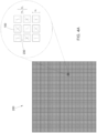
- Figs. 2A and 2B show a 3x3 array of nine pcLEDs, such arrays may include for example on the order of 10 2 , 10 3 , 10 4 , or more LEDs, e.g., as illustrated schematically in Fig. 4A .
- Individual LEDs 100 i.e., pixels
- LEDs 100 in the array 200 may be spaced apart from each other by streets, lanes, or trenches 230 having a width w 2 in the plane of the array 200 of, for example, , less than about 0.10 millimeters, less than about 0.05 millimeters, less than about 0.020 millimeters, less than about 0.010 millimeters, or less than about 0.005 millimeters.
- the pixel pitch D 1 is the sum of w 1 and w 2 .
- the illustrated examples show rectangular pixels arranged in a symmetric matrix, the pixels and the array may have any suitable shape or arrangement, whether symmetric or asymmetric. Multiple separate arrays of LEDs can be combined in any suitable arrangement in any applicable format to form a larger combined array or display.
- LEDs having dimensions w 1 in the plane of the array are typically referred to as microLEDs, and an array of such microLEDs may be referred to as a microLED array.
- LEDs having dimensions w 1 in the plane of the array e.g., side lengths of between about 0.10 millimeters and about 1.0 millimeters are typically referred to as miniLEDs, and an array of such miniLEDs may be referred to as a miniLED array.
- An array of LEDs, miniLEDs, or microLEDs, or portions of such an array may be formed as a segmented monolithic structure in which individual LED pixels are electrically isolated from each other by trenches, grooves, or streets, or by suitably arranged insulating material (e.g., filling the trenches).
- Figure 4B shows a perspective view of an example of such a segmented monolithic LED array 200. Pixels in this array (i.e., individual semiconductor LED devices 102) are separated by trenches 230 which are filled to form n-contacts 234.
- the monolithic structure is grown or disposed on the substrate 204.
- Each pixel includes a p-contact 236, a p-GaN semiconductor layer 102b, an active region 102a, and an n-GaN semiconductor layer 102c; the layers 102a/102b/102c collectively form the semiconductor LED 102.
- a wavelength converter material 106 may be deposited on the semiconductor layer 102c (or other applicable intervening layer).
- Passivation layers 232 may be formed within the trenches 230 to separate at least a portion of the n-contacts 234 from one or more layers of the semiconductor.
- the n-contacts 234, other material within the trenches 230, or material different from material within the trenches 230 may extend into the converter material 106 to form complete or partial optical isolation barriers 220 between the pixels.
- Fig. 4C is a schematic cross-sectional view of a close packed array 200 of multi-colored, phosphor converted LEDs 100 on a monolithic die and substrate 204.
- the side view shows GaN LEDs 102 attached to the substrate 204 through metal interconnects 239 (e.g., gold-gold interconnects or solder attached to copper micropillars) and metal interconnects 238.
- Phosphor pixels 106 are positioned on or over corresponding GaN LED pixels 102.
- the semiconductor LED pixels 102 or phosphor pixels 106 can be coated on their sides with a reflective mirror or diffusive scattering layer to form an optical isolation barrier 220.
- each phosphor pixel 106 is one of three different colors, e.g., red phosphor pixels 106R, green phosphor pixels 106G, and blue phosphor pixels 106B (still referred to generally or collectively as phosphor pixels 106).
- red phosphor pixels 106R red phosphor pixels 106R
- green phosphor pixels 106G green phosphor pixels 106G
- blue phosphor pixels 106B still referred to generally or collectively as phosphor pixels 106.
- the individual LEDs (pixels) in an LED array may be individually addressable, may be addressable as part of a group or subset of the pixels in the array, or may not be addressable.
- light emitting pixel arrays are useful for any application requiring or benefiting from fine-grained intensity, spatial, and temporal control of light distribution. These applications may include, but are not limited to, precise special patterning of emitted light from pixel blocks or individual pixels, in some instances including the formation of images as a display device.
- emitted light may be spectrally distinct, adaptive over time, and/or environmentally responsive.
- the light emitting pixel arrays may provide preprogrammed light distribution in various intensity, spatial, or temporal patterns. The emitted light may be based at least in part on received sensor data and may be used for optical wireless communications.
- Associated electronics and optics may be distinct at a pixel, pixel block, or device level.
- Figs. 5A and 5B are examples of LED arrays 200 employed in display applications, wherein an LED display includes a multitude of display pixels.
- each display pixel comprises a single semiconductor LED pixel 102 (not visible in Fig. 5A ) and a corresponding phosphor pixel 106R, 106G, or 106B of a single color (red, green, or blue).
- Each display pixel only provides one of the three colors.
- each display pixel includes multiple semiconductor LED pixels 102 (not visible in Fig. 5B ) and multiple corresponding phosphor pixels 106 of multiple colors.
- each display pixel includes a 3X3 array of semiconductor pixels 102; three of those LED pixels have red phosphor pixels 106R, three have green phosphor pixels 106G, and three have blue phosphor pixels 106B.
- Each display pixel can therefore produce any desired color combination.
- the spatial arrangement of the different colored phosphor pixels 106 differs among the display pixels; in some examples (not shown) each display pixel can have the same arrangement of the different colored phosphor pixels 106.
- a pcLED array 200 may be mounted on an electronics board 300 comprising a power and control module 302, a sensor module 304, and an LED attach region 306.
- Power and control module 302 may receive power and control signals from external sources and signals from sensor module 304, based on which power and control module 302 controls operation of the LEDs.
- Sensor module 304 may receive signals from any suitable sensors, for example from temperature or light sensors.
- pcLED array 200 may be mounted on a separate board (not shown) from the power and control module and the sensor module.
- a highly reflective side coating is often used in top emitter LED applications to redirect the light coming out through the side walls of the LED to a wavelength converting structure positioned on the top surface of the die. If the areas of the side walls of the LED die are of significant size, for example around 40% of photons generated by the die will go unconverted if there is no reflector coating located over the side wall areas.
- Such side coatings can be included in any of the examples shown, e.g., within trenches 230 or incorporated into barriers 220.
- One method for forming side wall reflectors is to apply a layer of light scattering particles mixed with a binder (e.g., silicone) onto the side walls, for example by dispensing or molding. Because reflection of light incident on such a reflector occurs through a series of reflection (scattering) or refraction events (often both), a long path length and correspondingly large thickness of the reflective layer perpendicular to the die often may be needed to provide sufficient reflection and extinction of excess light.
- a binder e.g., silicone
- Conventional side coat materials include TiO 2 powder particles in liquid silicone, and SiO 2 /Al 2 O 3 fiber or Glass fiber/TiO 2 /silicone molding compounds.
- transmission of these materials is such that if the reflector layer surrounding the die/converter has a thickness ⁇ 250 microns, blue photons from the LED and converted light from the wavelength converter can penetrate though the reflector. Photons that penetrate through the reflector can then be scattered by or absorbed in neighboring pcLEDs, a process referred to as cross-talk. Photons leaking through the reflector can also cause color shift of the pcLED or over-converted red output, or can adversely affect contrast.
- Some pcLED applications may require a thin side coat on the sides of the LED emitter (e.g., due to space constraints) and at the same time may be very sensitive to photons penetrating the thin side coat and causing color shift of and cross-talk between the pcLEDs of the array. This can be important for applications (automotive, flash, projection, display, etc.) where optical contrast is an important optical parameter.
- pcLEDs are arranged in an array with a narrow spacing (e.g., ⁇ 40 microns) between pcLEDs (e.g., as in a pc-miniLED array or a pc-microLED array)
- blue photons from the LEDs can in some instances penetrate through a thin TiO 2 /silicone layer between adjacent pcLEDs, causing cross-talk and color change in adjacent pixels of the pcLED array.
- Fig. 7 shows a simplified schematic cross-sectional view of several adjacent individual pcLED pixels 100 on a shared substrate 204 in a pcLED array 200.
- the pcLED array 200 may comprise many more such pcLED pixels arranged on a shared substrate 204, but only a few are shown here for simplicity of presentation.
- Each pcLED pixel 100 comprises a semiconductor LED pixel 102 disposed on the substrate 204, and a wavelength converting structure 106 (i.e., a phosphor pixel 106) disposed on the LED pixel 102.
- the pcLEDs 100 are spaced apart from each other by a street (i.e., a trench or gap; labelled trench 230 in Figs. 4A and 4B ; filled with barrier material 220 but not separately labelled in Fig. 7 ) having a width w 2 (e.g., as in Fig. 4A ).
- the streets may have widths w 2 of 5 to 30 microns, for example, or any other suitable width, including those disclosed above.
- Off-state white layers typically strongly scatter ambient light and consequently appear white when the pcLED is not operating, but become less scattering at the elevated temperatures resulting from pcLED operation.
- the streets are shown as being defined by straight parallel pcLED side walls oriented perpendicularly to the substrate 204, in other variations the LED side walls, the wavelength converter sidewalls, or both the LED side walls and the wavelength converter side walls may be angled with respect to the substrate 204.
- the streets may therefore by narrower toward the top light emitting surface of the pcLEDs 100 than near the substrate 204, or alternatively wider near the top light emitting surface of the pcLEDs 100 than near the substrate 204.
- the array of pcLED pixels 100 may be formed using any suitable methods.
- the streets between pixels may be formed for example by photoresist patterning, mechanical sawing, or laser patterning.
- the wavelength converting structures 106 may be formed directly on the LEDs 102, or an array of wavelength converters 106 may be separately formed and then attached to an array of LEDs 102 to form the array 200 of pcLED pixels 100.
- Each LED 102 comprises an active region disposed between n-type and p-type layers (e.g., layers 102a/102b/102c of Fig. 4B ).
- Application of a suitable forward bias across the diode structure results in emission of light from the active region.
- the LEDs may be, for example III-Nitride LEDs that emit blue, violet, or ultraviolet light. LEDs formed from any other suitable material system and that emit any other suitable wavelength of light may also be used.
- Other suitable material systems may include, e.g. III-Phosphide materials, III-Arsenide materials, and II-VI materials, as noted above.
- Wavelength converting structures 106 may comprise, for example, phosphor particles dispersed in a binder. Suitable binders may include silicones and solgels, for example. Alternatively, wavelength converting structures 106 may comprise ceramic phosphor structures, formed for example by sintering phosphor particles. Each wavelength converting structure 106 may comprise phosphors of only a single composition, or phosphors of two or more different compositions. Each pcLED 100 of the array 200 can have the same one or more phosphor materials are the other pcLEDs 100 of the array 200, or the one or more phosphor materials can differ among the pcLEDs 100 of the array 200. Phosphors in wavelength converting structure 106 may, for example, convert blue light to red, yellow, green, or cyan light. Any suitable phosphor materials may be used, depending on the desired optical output from the pcLEDs 100 of the array 200.
- Reflective side coats 220 are disposed on the sides of the pcLEDs, in the streets between adjacent pcLEDs 100. Reflective side coats 220 may fill the streets as shown in Figure 7 . Alternatively adjacent pcLEDs 100 may each have a side coat 220 in the street between the pixels, without completely filling the street (not shown). Such side coatings serve to at least partly isolate adjacent pcLEDs from one another, i.e., to reduce or prevent leakage of light emitted from a first pcLED into a second, adjacent pcLED, there to be scattered as part of the second pcLED's output or to be absorbed and cause unwanted emission that then forms part of the second pcLED's output.
- Such leakage or crosstalk is undesirable in applications wherein high contrast between adjacent pcLEDs is needed (e.g., for a pcLED array used as a display device). Such leakage or crosstalk can also alter the color profile or color point of pcLEDs of the array in uncontrolled or undesirable ways.
- Conventional side reflectors often include scattering particles, scattering voids, or reflective particles that redirect at least some of the light back toward the emitting pcLED and reduce or prevent propagation into an adjacent pcLED.
- Side reflector coating materials disclosed herein for use in side reflectors for pcLEDs comprise pigments that are photochemically stable under illumination by light from the pcLED.
- the pigments absorb light emitted by the pcLED.
- pigments is meant material that absorbs light and does not in response emit light of a longer wavelength. Pigments therefore differ from phosphors.
- the pigments absorb blue and green light and reflect red light, or absorb red light and reflect green light, or reflect blue light and absorb green light, or red light, or both.
- the side coating materials may comprise light scattering voids or light scattering particles (e.g., TiO 2 particles) dispersed in a transparent binder material (e.g., a silicone or a solgel) in which the pigments are also dispersed.
- a transparent binder material e.g., a silicone or a solgel
- the side coating material may optionally also comprise phosphor particles.
- the pigments may be inorganic or organic pigments.
- Side coatings and side coating materials as disclosed herein may be employed, for example, with pcLED arrays used in automotive, flash, illumination, and display applications.
- Side coatings including pigments can be advantageously employed in pcLED arrays wherein spacing between adjacent pcLEDs of the array might not provide sufficient light propagation pathlength to result in sufficient isolation.
- Such situations can arise in, e.g., pc-miniLED arrays or pc-microLED arrays as described above, wherein spacing between adjacent pcLEDs typically is less than about 0.10 millimeters, less than about 0.05 millimeters, or even less.
- addition of one or more pigments as disclosed or claimed herein can in some examples increase isolation to acceptable levels.
- reflective side coats 220 are formed from a material comprising pigments that are photochemically stable under illumination by light from the LED 102 and from the wavelength converting structure 106. These pigments absorb light from the pcLED 100, decreasing light leakage through the side walls. This allows effective isolation of adjacent pcLED pixels with much thinner reflective side walls than would be necessary without the pigments. Because the pigments can be chosen to selectively absorb only portions of the spectrum of light from the pcLED, they also may help tailor the color point of the pcLED.
- Suitable inorganic green pigments may include, for example, Co 2 TiO 4 , Zn 2 TiO 4 , Ni 2 TiO 4 , or (Co, Zn, Ni) 2 TiO 4 .
- Suitable inorganic red pigments may include, for example, BiO 4 V (bismuth vanadate).
- Suitable inorganic blue pigments may include, for example, CoAl 2 O 4 or YlnMn-blue.
- Suitable organic blue and green pigments may include, for example, phtalocyanines.
- Suitable organic red pigments may include, for example, perylenes. Other suitable pigments can be employed.
- the pigments may be dispersed with light scattering particles in a binder, and optionally with phosphor particles in the binder as well.
- An advantage of including phosphor particles is that when adjacent pcLED pixels are outputting light there would be less of a dark gap between the operating pixels, without use of external optics to blur the resolution.
- the phosphor particles in the reflective side coat may, for example, convert blue light from the LED to red, yellow, green, or cyan light.
- the side coating material may be applied to the pcLED array 200 to fill the streets by, for example, a dispensing, spraying, or molding process.
- Excess side coat material for example disposed on the light output top surface of a wavelength converting structure or on the light output top surface of an off-state white layer disposed on the wavelength converting structure, can be removed by mechanical abrasion, planarization, polishing or grinding, for example.
- the reflective side coat 220 may comprise, for example, TiO 2 light scattering particles, air voids, inorganic or organic pigments, and optionally phosphor particles, all dispersed homogeneously in a silicone or solgel binder matrix.
- the air voids may act as light scatterers, and may also reduce the refractive index of the binder matrix. In this variation the difference between the refractive index of the phosphor particles and the surrounding matrix is typically homogeneous throughout the reflector.
- the reflective side coat may comprise two or more layers oriented parallel to the sides of the pcLEDs 100.
- a first layer, disposed on the side of the pcLED, may comprise light scattering particles (and optionally air voids) dispersed in a transparent silicon or solgel matrix.
- a second layer, disposed on the first layer and spaced apart from the pcLED by the first layer, may comprise pigments dispersed in a transparent silicon or solgel matrix.
- the separate layers may comprise different binder matrices.
- Such a layered structure maximizes the light scattering/reflecting effect of the first (e.g., TiO 2 ) layer while maintaining the absorption/light extinguishing effect of the pigment containing layer.
- the layered structure can be made by sequential application of the first layer with a thickness less than the street width, followed by application of the second layer.
- the layering can also be performed by first filling the street with side coat material for the first layer, then sawing or etching a smaller street within the first layer, then filling the new street with the material for the second layer.
- the resulting layered reflective side coat structure between two adjacent pcLED pixels may comprise, for example, a first light scattering particle layer disposed on the side wall of one of the pcLED pixels, a second light scattering particle layer disposed on the side wall of the other of the adjacent pcLED pixels, and one or more pigment layers disposed between the first and second light scattering layers.
- Reflective side coat 220 may comprise additional layers between the two adjacent pcLED pixels 100, as suitable.
- phosphor particles may optionally be dispersed in the light scattering particle layer, in the pigment layer, or in both the light scattering layer and the pigment layer.
- the difference between the refractive index of the phosphor particles and the surrounding matrix may vary with distance from the pcLED side wall (e.g., have a gradient) because the matrix is layered rather than homogeneous and the matrix index of refraction may be different in different layers.
- the refractive index may for example vary gradually, or more strongly as for example a step function.
- Figs. 8A and 8B show, respectively, reflection and transmission spectra of side coat material samples comprising different concentrations (wgt% ranging from 0.00% to 0.5%) of approximately 0.5 to 1 micron diameter particles of blue absorbing pigment Fe 2 O 3 uniformly dispersed in a TiO 2 / silicone mixture.
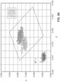
- FIG. 9A shows color point coordinates u' and v' for the output of pcLEDs having reflective side walls formed with these sample side coat materials, and demonstrates that increasing sidewall light absorption of blue light by sidewalls of increasing pigment concentration moves the color point of the pcLEDs to higher u' and v' color points.
- Fig. 9B shows that the increasing pigment concentrations reduces the total light output from the pcLEDs. Images of these pcLEDs in operation (not shown) demonstrate that side light leakage from the pcLEDs decreases with increasing pigment concentration in the side wall reflectors.
Landscapes
- Led Device Packages (AREA)
Description
- The invention relates generally to light emitting diodes and to phosphor-converted light emitting diodes.
- Semiconductor light emitting diodes and laser diodes (collectively referred to herein as "LEDs") are among the most efficient light sources currently available. The emission spectrum of an LED typically exhibits a single narrow peak at a wavelength determined by the structure of the device and by the composition of the semiconductor materials from which it is constructed. By suitable choice of device structure and material system, LEDs may be designed to operate at ultraviolet, visible, or infrared wavelengths.
- LEDs may be combined with one or more wavelength converting materials (generally referred to herein as "phosphors") that absorb light emitted by the LED and in response emit light of a longer wavelength. For such phosphor-converted LEDs ("pcLEDs"), the fraction of the light emitted by the LED that is absorbed by the phosphors depends on the amount of phosphor material in the optical path of the light emitted by the LED, for example on the concentration of phosphor material in a phosphor layer disposed on or around the LED and the thickness of the layer.
- Phosphor-converted LEDs may be designed so that all of the light emitted by the LED is absorbed by one or more phosphors, in which case the emission from the pcLED is entirely from the phosphors. In such cases the phosphor may be selected, for example, to emit light in a narrow spectral region that is not efficiently generated directly by an LED.
- Alternatively, pcLEDs may be designed so that only a portion of the light emitted by the LED is absorbed by the phosphors, in which case the emission from the pcLED is a mixture of light emitted by the LED and light emitted by the phosphors. By suitable choice of LED, phosphors, and phosphor composition, such a pcLED may be designed to emit, for example, white light having a desired color temperature and desired color-rendering properties.
- Multiple LEDs can be formed together on a single substrate to form an array. Such arrays can be employed to form active illuminated displays, such as those employed in smartphones and smart watches, computer or video displays, or signage. An array having one or several or many individual devices per millimeter (e.g., device pitch of about a millimeter, a few hundred microns, or less than 100 microns, and spacing between adjacent devices less than 100 microns or only a few tens of microns or less) typically is referred to as a miniLED array or a microLED array (alternatively, a µLED array). Such miniLED arrays or microLED arrays can in many instances also include phosphor converters as described above; such arrays can be referred to as pc-miniLED arrays or pc-microLED arrays.
-
US 2011/175117 A1 discloses a light emitting device comprising a light emitting diode arranged on a submount, said device having a lateral circumference surface and a top surface, and an optically active coating layer. Said coating layer covering along at least a part of said circumference surface, extending from the submount to said top surface, and essentially not covering the top surface. - The invention is set out in the appended set of claims. A light emitting device comprises a substrate, first and second phosphor converted LEDs, and a side reflector. Each of the first and second phosphor converted LEDs comprising a corresponding semiconductor LED, a corresponding wavelength converting structure, a light emitting external surface, and side walls. Each semiconductor LED is disposed on the substrate; each wavelength converting structure is disposed on a surface of the corresponding semiconductor LED opposite from the substrate. Each light emitting external surface is located opposite from the substrate, and the side walls extend from the substrate to the light emitting surface of each phosphor converted LED. The phosphor converted LEDs are spaced apart from each other by a street defined by the substrate and their corresponding side walls. The street is less than about 0.10 millimeters wide. The side reflector is disposed in the street on a side wall of the first phosphor converted LED and includes one or more pigments that absorb light in at least a portion of the spectrum of light emitted by the first phosphor converted LED. The street can be less than about 0.05 millimeters wide. The phosphor converted LEDs can be monolithically integrated together on the substrate, and can have transverse dimensions less than about 1.0 millimeters or less than about 0.10 millimeters.
- Objects and advantages pertaining to LEDs, pcLEDs, miniLED arrays, pc-miniLED arrays, microLED arrays, and pc-microLED arrays may become apparent upon referring to the examples illustrated in the drawings and disclosed in the following written description or appended claims.
- This Summary is provided to introduce a selection of concepts in a simplified form that are further described below in the Detailed Description. This Summary is not intended to identify key features or essential features of the claimed subject matter, nor is it intended to be used as an aid in determining the scope of the claimed subject matter.
-
-
Fig. 1 shows a schematic cross-sectional view of an example pcLED. -
Figs 2A and 2B show, respectively, cross-sectional and top schematic views of an example array of pcLEDs. -
Fig. 3A shows a schematic cross-sectional view of an example array of pcLEDs arranged with respect to waveguides and a projection lens.Fig. 3B shows an arrangement similar to that ofFigure 3A , but without the waveguides. -
Fig. 4A shows a top schematic view of an example miniLED or microLED array and an enlarged section of 3x3 LEDs of the array.Fig. 4B shows a perspective view of several LEDs of an example pc-miniLED or pc-microLED array monolithically formed on a substrate.Fig. 4C is a side cross-sectional schematic diagram of an example of a close-packed array of multi-colored phosphor-converted LEDS on a monolithic die and substrate. -
Fig. 5A is a schematic top view of a portion of an example LED display in which each display pixel is a red, green, or blue phosphor-converted LED pixel.Fig. 5B is a schematic top view of a portion of an example LED display in which each display pixel includes multiple phosphor-converted LED pixels (red, green, and blue) integrated onto a single die that is bonded to a control circuit backplane. -
Fig. 6A shows a schematic top view an example electronics board on which an array of pcLEDs may be mounted, andFig. 6B shows an example array of pcLEDs mounted on the electronic board ofFig. 6A . -
Fig. 7 shows a schematic cross-sectional view of a portion of an example pcLED array including pigmented and scattering side coating material between LED pixels. -
Fig. 8A shows reflection spectra of side coat material samples comprising different concentrations of a blue absorbing pigment;Fig. 8B shows corresponding transmission spectra for the samples ofFig. 8A . -
Fig. 9A shows color point coordinates u' and v' for the output of pcLEDs having reflective side walls formed with the sample side coat materials ofFigs. 8A and 8B ;Fig. 9B compares total light output from the pcLEDs ofFig. 9A . - The examples depicted are shown only schematically; all features may not be shown in full detail or in proper proportion; for clarity certain features or structures may be exaggerated or diminished relative to others or omitted entirely; the drawings should not be regarded as being to scale unless explicitly indicated as being to scale. For example, individual LEDs may be exaggerated in their vertical dimensions or layer thicknesses relative to their lateral extent or relative to substrate or phosphor thicknesses. The examples shown should not be construed as limiting the scope of the present disclosure or appended claims.
- The following detailed description should be read with reference to the drawings, in which identical reference numbers refer to like elements throughout the different figures. The drawings, which are not necessarily to scale, depict selective examples and are not intended to limit the scope of the invention. The detailed description illustrates inventive principles by way of example, not by way of limitation.
-
Fig. 1 shows an example of anindividual pcLED 100 comprising asemiconductor diode structure 102 disposed on asubstrate 104, together considered herein an "LED" or "semiconductor LED", and a wavelength converting structure 106 (e.g., phosphor layer) disposed on the semiconductor LED.Semiconductor diode structure 102 typically comprises an active region disposed between n-type and p-type layers. Application of a suitable forward bias across thediode structure 102 results in emission of light from the active region. The wavelength of the emitted light is determined by the composition and structure of the active region. - The LED may be, for example, a III-Nitride LED that emits blue, violet, or ultraviolet light. LEDs formed from any other suitable material system and that emit any other suitable wavelength of light may also be used. Suitable material systems may include, for example, various III-Nitride materials, various III-Phosphide materials, various III-Arsenide materials, and various II-VI materials.
- Any suitable phosphor materials may be used for or incorporated into the
wavelength converting structure 106, depending on the desired optical output from the pcLED. -
Figs. 2A-2B show, respectively, cross-sectional and top views of anarray 200 ofpcLEDs 100, each including aphosphor pixel 106, disposed on asubstrate 204. Such an array may include any suitable number of pcLEDs arranged in any suitable manner. In the illustrated examples the array is depicted as formed monolithically on a shared substrate, but alternatively an array of pcLEDs may be formed from separate individual pcLEDs.Substrate 204 may optionally include electrical traces or interconnects, or CMOS or other circuitry for driving the LED, and may be formed from any suitable materials. -
Individual pcLEDs 100 may optionally incorporate or be arranged in combination with a lens or other optical element located adjacent to or disposed on the phosphor layer. Such an optical element, not shown in the figures, may be referred to as a "primary optical element". In addition, as shown inFigures 3A and 3B , a pcLED array 200 (for example, mounted on an electronics board) may be arranged in combination with secondary optical elements such as waveguides, lenses, or both for use in an intended application. InFigure 3A , light emitted by eachpcLED 100 of thearray 200 is collected by a correspondingwaveguide 192 and directed to aprojection lens 294.Projection lens 294 may be a Fresnel lens, for example. This arrangement may be suitable for use, for example, in automobile headlights. InFigure 3B , light emitted by pcLEDs of thearray 200 is collected directly byprojection lens 294 without use of intervening waveguides. This arrangement may particularly be suitable when pcLEDs can be spaced sufficiently close to each other, and may also be used in automobile headlights as well as in camera flash applications. A miniLED or microLED display application may use similar optical arrangements to those depicted inFigs. 3A and 3B , for example. Generally, any suitable arrangement of optical elements may be used in combination with the pcLEDs described herein, depending on the desired application. - Although
Figs. 2A and 2B show a 3x3 array of nine pcLEDs, such arrays may include for example on the order of 102, 103, 104, or more LEDs, e.g., as illustrated schematically inFig. 4A . Individual LEDs 100 (i.e., pixels) may have widths w1 (e.g., side lengths) in the plane of thearray 200, for example, less than about 1.0 millimeters, less than about 0.5 millimeters, less than about 0.10 millimeters, or less than about 0.05 millimeters.LEDs 100 in thearray 200 may be spaced apart from each other by streets, lanes, ortrenches 230 having a width w2 in the plane of thearray 200 of, for example, , less than about 0.10 millimeters, less than about 0.05 millimeters, less than about 0.020 millimeters, less than about 0.010 millimeters, or less than about 0.005 millimeters. The pixel pitch D1 is the sum of w1 and w2. Although the illustrated examples show rectangular pixels arranged in a symmetric matrix, the pixels and the array may have any suitable shape or arrangement, whether symmetric or asymmetric. Multiple separate arrays of LEDs can be combined in any suitable arrangement in any applicable format to form a larger combined array or display. - LEDs having dimensions w1 in the plane of the array (e.g., side lengths) of less than or equal to about 0.10 millimeters microns are typically referred to as microLEDs, and an array of such microLEDs may be referred to as a microLED array. LEDs having dimensions w1 in the plane of the array (e.g., side lengths) of between about 0.10 millimeters and about 1.0 millimeters are typically referred to as miniLEDs, and an array of such miniLEDs may be referred to as a miniLED array.
- An array of LEDs, miniLEDs, or microLEDs, or portions of such an array, may be formed as a segmented monolithic structure in which individual LED pixels are electrically isolated from each other by trenches, grooves, or streets, or by suitably arranged insulating material (e.g., filling the trenches).
Figure 4B shows a perspective view of an example of such a segmentedmonolithic LED array 200. Pixels in this array (i.e., individual semiconductor LED devices 102) are separated bytrenches 230 which are filled to form n-contacts 234. The monolithic structure is grown or disposed on thesubstrate 204. Each pixel includes a p-contact 236, a p-GaN semiconductor layer 102b, anactive region 102a, and an n-GaN semiconductor layer 102c; thelayers 102a/102b/102c collectively form thesemiconductor LED 102. Awavelength converter material 106 may be deposited on thesemiconductor layer 102c (or other applicable intervening layer). Passivation layers 232 may be formed within thetrenches 230 to separate at least a portion of the n-contacts 234 from one or more layers of the semiconductor. The n-contacts 234, other material within thetrenches 230, or material different from material within thetrenches 230 may extend into theconverter material 106 to form complete or partialoptical isolation barriers 220 between the pixels. -
Fig. 4C is a schematic cross-sectional view of a close packedarray 200 of multi-colored, phosphor convertedLEDs 100 on a monolithic die andsubstrate 204. The side view showsGaN LEDs 102 attached to thesubstrate 204 through metal interconnects 239 (e.g., gold-gold interconnects or solder attached to copper micropillars) and metal interconnects 238.Phosphor pixels 106 are positioned on or over correspondingGaN LED pixels 102. Thesemiconductor LED pixels 102 or phosphor pixels 106 (often both) can be coated on their sides with a reflective mirror or diffusive scattering layer to form anoptical isolation barrier 220. In this example eachphosphor pixel 106 is one of three different colors, e.g.,red phosphor pixels 106R,green phosphor pixels 106G, andblue phosphor pixels 106B (still referred to generally or collectively as phosphor pixels 106). Such an arrangement can enable use of theLED array 200 as a color display. - The individual LEDs (pixels) in an LED array may be individually addressable, may be addressable as part of a group or subset of the pixels in the array, or may not be addressable. Thus, light emitting pixel arrays are useful for any application requiring or benefiting from fine-grained intensity, spatial, and temporal control of light distribution. These applications may include, but are not limited to, precise special patterning of emitted light from pixel blocks or individual pixels, in some instances including the formation of images as a display device. Depending on the application, emitted light may be spectrally distinct, adaptive over time, and/or environmentally responsive. The light emitting pixel arrays may provide preprogrammed light distribution in various intensity, spatial, or temporal patterns. The emitted light may be based at least in part on received sensor data and may be used for optical wireless communications. Associated electronics and optics may be distinct at a pixel, pixel block, or device level.
-
Figs. 5A and 5B are examples ofLED arrays 200 employed in display applications, wherein an LED display includes a multitude of display pixels. In some examples (e.g., as inFig. 5A ), each display pixel comprises a single semiconductor LED pixel 102 (not visible inFig. 5A ) and acorresponding phosphor pixel Fig. 5B ), each display pixel includes multiple semiconductor LED pixels 102 (not visible inFig. 5B ) and multiplecorresponding phosphor pixels 106 of multiple colors. In the example shown each display pixel includes a 3X3 array ofsemiconductor pixels 102; three of those LED pixels havered phosphor pixels 106R, three havegreen phosphor pixels 106G, and three have bluephosphor pixels 106B. Each display pixel can therefore produce any desired color combination. In the example shown the spatial arrangement of the differentcolored phosphor pixels 106 differs among the display pixels; in some examples (not shown) each display pixel can have the same arrangement of the differentcolored phosphor pixels 106. - As shown in
Figs. 6A and 6B , apcLED array 200 may be mounted on anelectronics board 300 comprising a power andcontrol module 302, asensor module 304, and an LED attachregion 306. Power andcontrol module 302 may receive power and control signals from external sources and signals fromsensor module 304, based on which power andcontrol module 302 controls operation of the LEDs.Sensor module 304 may receive signals from any suitable sensors, for example from temperature or light sensors. Alternatively,pcLED array 200 may be mounted on a separate board (not shown) from the power and control module and the sensor module. - A highly reflective side coating is often used in top emitter LED applications to redirect the light coming out through the side walls of the LED to a wavelength converting structure positioned on the top surface of the die. If the areas of the side walls of the LED die are of significant size, for example around 40% of photons generated by the die will go unconverted if there is no reflector coating located over the side wall areas. Such side coatings can be included in any of the examples shown, e.g., within
trenches 230 or incorporated intobarriers 220. - One method for forming side wall reflectors is to apply a layer of light scattering particles mixed with a binder (e.g., silicone) onto the side walls, for example by dispensing or molding. Because reflection of light incident on such a reflector occurs through a series of reflection (scattering) or refraction events (often both), a long path length and correspondingly large thickness of the reflective layer perpendicular to the die often may be needed to provide sufficient reflection and extinction of excess light.
- Conventional side coat materials include TiO2 powder particles in liquid silicone, and SiO2/Al2O3 fiber or Glass fiber/TiO2/silicone molding compounds. In some examples transmission of these materials is such that if the reflector layer surrounding the die/converter has a thickness < 250 microns, blue photons from the LED and converted light from the wavelength converter can penetrate though the reflector. Photons that penetrate through the reflector can then be scattered by or absorbed in neighboring pcLEDs, a process referred to as cross-talk. Photons leaking through the reflector can also cause color shift of the pcLED or over-converted red output, or can adversely affect contrast.
- Some pcLED applications may require a thin side coat on the sides of the LED emitter (e.g., due to space constraints) and at the same time may be very sensitive to photons penetrating the thin side coat and causing color shift of and cross-talk between the pcLEDs of the array. This can be important for applications (automotive, flash, projection, display, etc.) where optical contrast is an important optical parameter. For example, if pcLEDs are arranged in an array with a narrow spacing (e.g., <40 microns) between pcLEDs (e.g., as in a pc-miniLED array or a pc-microLED array), blue photons from the LEDs can in some instances penetrate through a thin TiO2/silicone layer between adjacent pcLEDs, causing cross-talk and color change in adjacent pixels of the pcLED array.
- Inventive arrangements according to the present disclosure or claims are discussed with respect to the device shown in
Fig. 7 , but are applicable to any pcLED array, pc-miniLED array, or pc-microLED array, including the other examples shown in the drawings.Fig. 7 shows a simplified schematic cross-sectional view of several adjacentindividual pcLED pixels 100 on a sharedsubstrate 204 in apcLED array 200. ThepcLED array 200 may comprise many more such pcLED pixels arranged on a sharedsubstrate 204, but only a few are shown here for simplicity of presentation. EachpcLED pixel 100 comprises asemiconductor LED pixel 102 disposed on thesubstrate 204, and a wavelength converting structure 106 (i.e., a phosphor pixel 106) disposed on theLED pixel 102. ThepcLEDs 100 are spaced apart from each other by a street (i.e., a trench or gap; labelledtrench 230 inFigs. 4A and4B ; filled withbarrier material 220 but not separately labelled inFig. 7 ) having a width w2 (e.g., as inFig. 4A ). The streets may have widths w2 of 5 to 30 microns, for example, or any other suitable width, including those disclosed above. An optional off state white layer, not shown, may be disposed on the top light output surface of eachwavelength converting structure 106. Off-state white layers typically strongly scatter ambient light and consequently appear white when the pcLED is not operating, but become less scattering at the elevated temperatures resulting from pcLED operation. - Although in
Fig. 7 the streets are shown as being defined by straight parallel pcLED side walls oriented perpendicularly to thesubstrate 204, in other variations the LED side walls, the wavelength converter sidewalls, or both the LED side walls and the wavelength converter side walls may be angled with respect to thesubstrate 204. The streets may therefore by narrower toward the top light emitting surface of thepcLEDs 100 than near thesubstrate 204, or alternatively wider near the top light emitting surface of thepcLEDs 100 than near thesubstrate 204. - The array of
pcLED pixels 100 may be formed using any suitable methods. The streets between pixels may be formed for example by photoresist patterning, mechanical sawing, or laser patterning. Thewavelength converting structures 106 may be formed directly on theLEDs 102, or an array ofwavelength converters 106 may be separately formed and then attached to an array ofLEDs 102 to form thearray 200 ofpcLED pixels 100. - Each
LED 102 comprises an active region disposed between n-type and p-type layers (e.g.,layers 102a/102b/102c ofFig. 4B ). Application of a suitable forward bias across the diode structure results in emission of light from the active region. The LEDs may be, for example III-Nitride LEDs that emit blue, violet, or ultraviolet light. LEDs formed from any other suitable material system and that emit any other suitable wavelength of light may also be used. Other suitable material systems may include, e.g. III-Phosphide materials, III-Arsenide materials, and II-VI materials, as noted above. -
Wavelength converting structures 106 may comprise, for example, phosphor particles dispersed in a binder. Suitable binders may include silicones and solgels, for example. Alternatively,wavelength converting structures 106 may comprise ceramic phosphor structures, formed for example by sintering phosphor particles. Eachwavelength converting structure 106 may comprise phosphors of only a single composition, or phosphors of two or more different compositions. EachpcLED 100 of thearray 200 can have the same one or more phosphor materials are theother pcLEDs 100 of thearray 200, or the one or more phosphor materials can differ among thepcLEDs 100 of thearray 200. Phosphors inwavelength converting structure 106 may, for example, convert blue light to red, yellow, green, or cyan light. Any suitable phosphor materials may be used, depending on the desired optical output from thepcLEDs 100 of thearray 200. -
Reflective side coats 220 are disposed on the sides of the pcLEDs, in the streets betweenadjacent pcLEDs 100.Reflective side coats 220 may fill the streets as shown inFigure 7 . Alternativelyadjacent pcLEDs 100 may each have aside coat 220 in the street between the pixels, without completely filling the street (not shown). Such side coatings serve to at least partly isolate adjacent pcLEDs from one another, i.e., to reduce or prevent leakage of light emitted from a first pcLED into a second, adjacent pcLED, there to be scattered as part of the second pcLED's output or to be absorbed and cause unwanted emission that then forms part of the second pcLED's output. Such leakage or crosstalk is undesirable in applications wherein high contrast between adjacent pcLEDs is needed (e.g., for a pcLED array used as a display device). Such leakage or crosstalk can also alter the color profile or color point of pcLEDs of the array in uncontrolled or undesirable ways. Conventional side reflectors often include scattering particles, scattering voids, or reflective particles that redirect at least some of the light back toward the emitting pcLED and reduce or prevent propagation into an adjacent pcLED. - Side reflector coating materials disclosed herein for use in side reflectors for pcLEDs comprise pigments that are photochemically stable under illumination by light from the pcLED. The pigments absorb light emitted by the pcLED. By pigments is meant material that absorbs light and does not in response emit light of a longer wavelength. Pigments therefore differ from phosphors. In the invention, the pigments absorb blue and green light and reflect red light, or absorb red light and reflect green light, or reflect blue light and absorb green light, or red light, or both. The side coating materials may comprise light scattering voids or light scattering particles (e.g., TiO2 particles) dispersed in a transparent binder material (e.g., a silicone or a solgel) in which the pigments are also dispersed. The side coating material may optionally also comprise phosphor particles. The pigments may be inorganic or organic pigments.
- Small concentrations of pigments in such side coating materials can help to decrease light leakage through the side walls and also help to tailor the color point of the pcLED. For thin-film flip-chip LEDs lacking a sapphire substrate the advantages of these pigments may be more substantial.
- Side coatings and side coating materials as disclosed herein may be employed, for example, with pcLED arrays used in automotive, flash, illumination, and display applications. Side coatings including pigments can be advantageously employed in pcLED arrays wherein spacing between adjacent pcLEDs of the array might not provide sufficient light propagation pathlength to result in sufficient isolation. Such situations can arise in, e.g., pc-miniLED arrays or pc-microLED arrays as described above, wherein spacing between adjacent pcLEDs typically is less than about 0.10 millimeters, less than about 0.05 millimeters, or even less. If reflective or scattering particles alone do not provide sufficient isolation between adjacent pcLEDs of the array, addition of one or more pigments as disclosed or claimed herein can in some examples increase isolation to acceptable levels.
- As summarized above, reflective side coats 220 are formed from a material comprising pigments that are photochemically stable under illumination by light from the
LED 102 and from thewavelength converting structure 106. These pigments absorb light from thepcLED 100, decreasing light leakage through the side walls. This allows effective isolation of adjacent pcLED pixels with much thinner reflective side walls than would be necessary without the pigments. Because the pigments can be chosen to selectively absorb only portions of the spectrum of light from the pcLED, they also may help tailor the color point of the pcLED. - Suitable inorganic green pigments (absorbing blue and red light) may include, for example, Co2TiO4, Zn2TiO4, Ni2TiO4, or (Co, Zn, Ni)2TiO4. Suitable inorganic red pigments (absorbing blue and green light) may include, for example, BiO4V (bismuth vanadate). Suitable inorganic blue pigments (absorbing green and red light) may include, for example, CoAl2O4 or YlnMn-blue. Suitable organic blue and green pigments may include, for example, phtalocyanines. Suitable organic red pigments may include, for example, perylenes. Other suitable pigments can be employed.
- Also as summarized above, the pigments may be dispersed with light scattering particles in a binder, and optionally with phosphor particles in the binder as well. An advantage of including phosphor particles is that when adjacent pcLED pixels are outputting light there would be less of a dark gap between the operating pixels, without use of external optics to blur the resolution. The phosphor particles in the reflective side coat may, for example, convert blue light from the LED to red, yellow, green, or cyan light.
- The side coating material may be applied to the
pcLED array 200 to fill the streets by, for example, a dispensing, spraying, or molding process. Excess side coat material, for example disposed on the light output top surface of a wavelength converting structure or on the light output top surface of an off-state white layer disposed on the wavelength converting structure, can be removed by mechanical abrasion, planarization, polishing or grinding, for example. - After deposition, the
reflective side coat 220 may comprise, for example, TiO2 light scattering particles, air voids, inorganic or organic pigments, and optionally phosphor particles, all dispersed homogeneously in a silicone or solgel binder matrix. The air voids may act as light scatterers, and may also reduce the refractive index of the binder matrix. In this variation the difference between the refractive index of the phosphor particles and the surrounding matrix is typically homogeneous throughout the reflector. - Alternatively, the reflective side coat may comprise two or more layers oriented parallel to the sides of the
pcLEDs 100. A first layer, disposed on the side of the pcLED, may comprise light scattering particles (and optionally air voids) dispersed in a transparent silicon or solgel matrix. A second layer, disposed on the first layer and spaced apart from the pcLED by the first layer, may comprise pigments dispersed in a transparent silicon or solgel matrix. The separate layers may comprise different binder matrices. Such a layered structure maximizes the light scattering/reflecting effect of the first (e.g., TiO2) layer while maintaining the absorption/light extinguishing effect of the pigment containing layer. - The layered structure can be made by sequential application of the first layer with a thickness less than the street width, followed by application of the second layer. The layering can also be performed by first filling the street with side coat material for the first layer, then sawing or etching a smaller street within the first layer, then filling the new street with the material for the second layer.
- The resulting layered reflective side coat structure between two adjacent pcLED pixels may comprise, for example, a first light scattering particle layer disposed on the side wall of one of the pcLED pixels, a second light scattering particle layer disposed on the side wall of the other of the adjacent pcLED pixels, and one or more pigment layers disposed between the first and second light scattering layers.
Reflective side coat 220 may comprise additional layers between the two adjacentpcLED pixels 100, as suitable. In such a layered structure, phosphor particles may optionally be dispersed in the light scattering particle layer, in the pigment layer, or in both the light scattering layer and the pigment layer. - In a layered side coat reflective structure as just described, the difference between the refractive index of the phosphor particles and the surrounding matrix may vary with distance from the pcLED side wall (e.g., have a gradient) because the matrix is layered rather than homogeneous and the matrix index of refraction may be different in different layers. Depending on the layer structure, the refractive index may for example vary gradually, or more strongly as for example a step function.
-
Figs. 8A and 8B show, respectively, reflection and transmission spectra of side coat material samples comprising different concentrations (wgt% ranging from 0.00% to 0.5%) of approximately 0.5 to 1 micron diameter particles of blue absorbing pigment Fe2O3 uniformly dispersed in a TiO2/ silicone mixture. -
FIG. 9A shows color point coordinates u' and v' for the output of pcLEDs having reflective side walls formed with these sample side coat materials, and demonstrates that increasing sidewall light absorption of blue light by sidewalls of increasing pigment concentration moves the color point of the pcLEDs to higher u' and v' color points.Fig. 9B shows that the increasing pigment concentrations reduces the total light output from the pcLEDs. Images of these pcLEDs in operation (not shown) demonstrate that side light leakage from the pcLEDs decreases with increasing pigment concentration in the side wall reflectors.
Claims (14)
- A light emitting device comprising:a substrate (204);a first phosphor converted LED comprising a first semiconductor LED (102) disposed on the substrate (204), a first wavelength converting structure (106) disposed on a surface of the first semiconductor LED (102) opposite from the substrate (204), a light emitting external surface located opposite from the substrate (204), and side walls extending from the substrate (204) to the light emitting surface;a second phosphor converted LED comprising a second semiconductor LED (102) disposed on the substrate (204), a second wavelength converting structure (106) disposed on a surface of the second semiconductor LED opposite from the substrate (204), a light emitting external surface opposite from the substrate (204), and side walls extending from the substrate (204) to the light emitting surface, the second phosphor converted LED being spaced apart from the first phosphor converted LED by a street (230) defined by the substrate (204), a side wall of the first phosphor converted LED, and an adjacent side wall of the second phosphor converted LED; wherein the first phosphor converted LED emits blue light, green light or red light;characterized bythe street (230) being less than 0.10 millimeters wide;a side reflector (220) disposed in the street (230) on a side wall of the first phosphor converted LED and including one or more pigments that absorb light in at least a portion of the spectrum of light emitted by the first phosphor converted LED; andwherein one or more of the pigments (i) absorb green and blue light and reflect red light, (ii) absorb red light and reflect green light, or (iii) reflect blue light and absorb green light, red light, or both.
- The light emitting device of claim 1 wherein the first and second phosphor converted LEDs are monolithically integrated on the substrate (204) and have transverse dimensions less than about 1.0 millimeters.
- The light emitting device of claim 2, wherein the first and second phosphor converted LEDs have transverse dimensions less than about 0.10 millimeters, and the street (230) is less than about 0.050 millimeters wide.
- The light emitting device of any one of claims 1 through 3, wherein the one or more pigments are dispersed in a transparent binder material.
- The light emitting device of any one of claims 1 through 4, wherein the side reflector (220) includes light scattering particles or air voids in a transparent binder material.
- The light emitting device of claim 5, wherein the one or more pigments and the light scattering particles are distributed homogenously in the transparent binder material.
- The light emitting device of claim 6, comprising phosphor particles distributed homogeneously in the transparent binder material.
- The light emitting device of any one of claims 4 through 7, wherein the transparent binder material is in contact with the adjacent side wall of the second phosphor converted LED and fills the street (230).
- The light emitting device of claim 5, wherein:the light scattering particles are dispersed in a first layer of transparent binder material disposed on the side of the first phosphor converted LED; andthe pigments are dispersed in a second layer of transparent binder material disposed on the first layer opposite from the side wall of the first phosphor converted LED.
- The light emitting device of claim 5, wherein:a first plurality of the light scattering particles is dispersed in a first layer of transparent binder material disposed on the side of the first phosphor converted LED;a second plurality of the light scattering particles is dispersed in a second layer of transparent binder material disposed on the adjacent side of the second phosphor converted LED;the pigments are disposed in a third layer of transparent binder material disposed between the first layer and the second layer; andthe side reflector fills the street (230).
- The light emitting device of claim 10, comprising a first plurality of phosphor particles dispersed in the transparent binder material of the first layer and a second plurality of phosphor particles dispersed in the transparent binder material of the second layer.
- A method for making the light emitting device of any one of Claims 1 through 11, the method comprising depositing in the street on a side wall of the first phosphor converted LED the side reflector that includes the one or more pigments.
- A method for making the light emitting device of claims 12, the method comprising:depositing on or applying to the side wall of the first phosphor converted LED a transparent binder material that includes light scattering particles dispersed therein;depositing on or applying to the side wall of the second phosphor converted LED a transparent binder material that includes light scattering particles dispersed therein; andfilling a space remaining between the binder materials on the respective side walls a transparent binder material that includes the one or more pigments dispersed therein.
- A method for making the light emitting device of any one of Claims 12 or 13, the method comprising:filling the street with a transparent binder material that includes light scattering particles dispersed therein;cutting or etching a groove or trench in the transparent binder material so as to leave binder material on both side walls of the street; andfilling the groove or trench with a transparent binder material that includes the one or more pigments dispersed therein.
Applications Claiming Priority (4)
| Application Number | Priority Date | Filing Date | Title |
|---|---|---|---|
| US16/664,617 US11302849B2 (en) | 2019-10-25 | 2019-10-25 | Pigmented and scattering particles in side coating materials for LED applications |
| EP20157143 | 2020-02-13 | ||
| US17/077,928 US11411043B2 (en) | 2019-10-25 | 2020-10-22 | Pigmented and scattering particles in side coating materials for LED applications |
| PCT/US2020/057015 WO2021081300A1 (en) | 2019-10-25 | 2020-10-23 | Pigmented and scattering particles in side coating materials for led applications |
Publications (2)
| Publication Number | Publication Date |
|---|---|
| EP4049312A1 EP4049312A1 (en) | 2022-08-31 |
| EP4049312B1 true EP4049312B1 (en) | 2024-09-18 |
Family
ID=73043326
Family Applications (1)
| Application Number | Title | Priority Date | Filing Date |
|---|---|---|---|
| EP20800770.8A Active EP4049312B1 (en) | 2019-10-25 | 2020-10-23 | Pigmented and scattering particles in side coating materials for led applications |
Country Status (3)
| Country | Link |
|---|---|
| US (2) | US11411043B2 (en) |
| EP (1) | EP4049312B1 (en) |
| WO (1) | WO2021081300A1 (en) |
Families Citing this family (9)
| Publication number | Priority date | Publication date | Assignee | Title |
|---|---|---|---|---|
| US11411043B2 (en) * | 2019-10-25 | 2022-08-09 | Lumileds Llc | Pigmented and scattering particles in side coating materials for LED applications |
| KR20220060912A (en) * | 2020-11-05 | 2022-05-12 | 삼성전자주식회사 | Nanorod type mirco-LED, pixel plate including the same and display and electronic devices including pixel plate |
| US20220199857A1 (en) * | 2020-12-17 | 2022-06-23 | Seoul Viosys Co., Ltd. | Unit pixel and displaying apparatus including the unit pixel |
| US11631715B2 (en) * | 2021-03-11 | 2023-04-18 | Lumileds Llc | Monolithic multi-color matrix emitter with patterned phosphor layer |
| WO2023076349A1 (en) * | 2021-10-29 | 2023-05-04 | Lumileds Llc | Patterned deposition mask formed using polymer dispersed in a liquid solvent |
| US12408496B2 (en) | 2021-10-29 | 2025-09-02 | Lumileds Singapore Pte. Ltd. | Patterned deposition mask formed using polymer dispersed in a liquid solvent |
| CN118648126A (en) * | 2021-12-03 | 2024-09-13 | 亮锐有限责任公司 | Reduction of crack sensitivity in porous optical layers |
| US20230178690A1 (en) * | 2021-12-06 | 2023-06-08 | Lumileds Llc | Monolithic LED Array And Method Of Manufacturing Thereof |
| WO2023114000A1 (en) * | 2021-12-15 | 2023-06-22 | Lumileds Llc | Reducing crosstalk and improving contrast in led and pcled arrays |
Family Cites Families (15)
| Publication number | Priority date | Publication date | Assignee | Title |
|---|---|---|---|---|
| WO2007039849A1 (en) | 2005-10-05 | 2007-04-12 | Philips Intellectual Property & Standards Gmbh | Phosphor-converted electroluminescent device with absorbing filter |
| RU2503092C2 (en) | 2008-09-25 | 2013-12-27 | Конинклейке Филипс Электроникс Н.В. | Coated light-emitting device and method of coating said device |
| JP5857746B2 (en) | 2009-12-22 | 2016-02-10 | 三菱化学株式会社 | Materials for resin moldings for semiconductor light emitting devices |
| US9484504B2 (en) | 2013-05-14 | 2016-11-01 | Apple Inc. | Micro LED with wavelength conversion layer |
| US9111464B2 (en) | 2013-06-18 | 2015-08-18 | LuxVue Technology Corporation | LED display with wavelength conversion layer |
| US10224358B2 (en) | 2017-05-09 | 2019-03-05 | Lumileds Llc | Light emitting device with reflective sidewall |
| KR101890582B1 (en) | 2017-12-14 | 2018-08-22 | 엘지디스플레이 주식회사 | Light emitting chip, micro display device |
| US11296262B2 (en) | 2017-12-21 | 2022-04-05 | Lumileds Llc | Monolithic segmented LED array architecture with reduced area phosphor emission surface |
| EP3776674B1 (en) | 2018-06-04 | 2024-07-31 | CreeLED, Inc. | Led apparatuses, and method |
| EP3608959B1 (en) | 2018-08-06 | 2023-11-15 | Nichia Corporation | Light emitting device and method for manufacturing same |
| KR102698293B1 (en) * | 2018-11-27 | 2024-08-23 | 삼성전자주식회사 | Display apparatus and method of manufacturing the same |
| US10910433B2 (en) | 2018-12-31 | 2021-02-02 | Lumileds Llc | Pixelated LED array with optical elements |
| EP3915151B1 (en) | 2019-01-25 | 2023-08-23 | Lumileds LLC | Method of manufacturing a wavelength-converting pixel array structure |
| US11411043B2 (en) * | 2019-10-25 | 2022-08-09 | Lumileds Llc | Pigmented and scattering particles in side coating materials for LED applications |
| US11302849B2 (en) | 2019-10-25 | 2022-04-12 | Lumileds Llc | Pigmented and scattering particles in side coating materials for LED applications |
-
2020
- 2020-10-22 US US17/077,928 patent/US11411043B2/en active Active
- 2020-10-23 WO PCT/US2020/057015 patent/WO2021081300A1/en not_active Ceased
- 2020-10-23 EP EP20800770.8A patent/EP4049312B1/en active Active
-
2022
- 2022-07-07 US US17/859,361 patent/US12027566B2/en active Active
Also Published As
| Publication number | Publication date |
|---|---|
| WO2021081300A1 (en) | 2021-04-29 |
| US11411043B2 (en) | 2022-08-09 |
| US20210126042A1 (en) | 2021-04-29 |
| US20220336522A1 (en) | 2022-10-20 |
| EP4049312A1 (en) | 2022-08-31 |
| US12027566B2 (en) | 2024-07-02 |
Similar Documents
| Publication | Publication Date | Title |
|---|---|---|
| US12027566B2 (en) | Pigmented and scattering particles in side coating materials for LED applications | |
| KR102699889B1 (en) | Light-emitting diodes having reflective sidewalls containing porous particles | |
| EP3900056B1 (en) | Led package with increased contrast ratio and method of manufacturing the same | |
| EP4042483B1 (en) | Optical coupling layer to improve output flux in light emitting diode arrays | |
| KR102935416B1 (en) | pixelated wavelength conversion layer | |
| KR102730680B1 (en) | Reduction of the appearance of defective pixels in luminescent arrays | |
| US11600751B2 (en) | Light-emitting semiconductor component and method for producing a light-emitting semiconductor component | |
| US20220285594A1 (en) | Light emitting diodes with reflective sidewalls comprising porous particles | |
| US12284850B2 (en) | Laterally heterogenous wavelength-converting layer | |
| US11302849B2 (en) | Pigmented and scattering particles in side coating materials for LED applications | |
| CN116210082B (en) | Coloring and scattering particles in side coating materials for LED applications | |
| US20260123151A1 (en) | Led array with air-spaced optics | |
| WO2022132192A1 (en) | Primary optics array for a light-emitting array | |
| EP4449509B1 (en) | Phosphor-converted light-emitting diode with dielectric spacer and method for making phosphor-converted light-emitting diode with dielectric spacer |
Legal Events
| Date | Code | Title | Description |
|---|---|---|---|
| STAA | Information on the status of an ep patent application or granted ep patent |
Free format text: STATUS: UNKNOWN |
|
| STAA | Information on the status of an ep patent application or granted ep patent |
Free format text: STATUS: THE INTERNATIONAL PUBLICATION HAS BEEN MADE |
|
| PUAI | Public reference made under article 153(3) epc to a published international application that has entered the european phase |
Free format text: ORIGINAL CODE: 0009012 |
|
| STAA | Information on the status of an ep patent application or granted ep patent |
Free format text: STATUS: REQUEST FOR EXAMINATION WAS MADE |
|
| 17P | Request for examination filed |
Effective date: 20220525 |
|
| AK | Designated contracting states |
Kind code of ref document: A1 Designated state(s): AL AT BE BG CH CY CZ DE DK EE ES FI FR GB GR HR HU IE IS IT LI LT LU LV MC MK MT NL NO PL PT RO RS SE SI SK SM TR |
|
| STAA | Information on the status of an ep patent application or granted ep patent |
Free format text: STATUS: EXAMINATION IS IN PROGRESS |
|
| DAV | Request for validation of the european patent (deleted) | ||
| DAX | Request for extension of the european patent (deleted) | ||
| 17Q | First examination report despatched |
Effective date: 20230120 |
|
| P01 | Opt-out of the competence of the unified patent court (upc) registered |
Effective date: 20230530 |
|
| GRAP | Despatch of communication of intention to grant a patent |
Free format text: ORIGINAL CODE: EPIDOSNIGR1 |
|
| STAA | Information on the status of an ep patent application or granted ep patent |
Free format text: STATUS: GRANT OF PATENT IS INTENDED |
|
| INTG | Intention to grant announced |
Effective date: 20240411 |
|
| GRAS | Grant fee paid |
Free format text: ORIGINAL CODE: EPIDOSNIGR3 |
|
| GRAA | (expected) grant |
Free format text: ORIGINAL CODE: 0009210 |
|
| STAA | Information on the status of an ep patent application or granted ep patent |
Free format text: STATUS: THE PATENT HAS BEEN GRANTED |
|
| AK | Designated contracting states |
Kind code of ref document: B1 Designated state(s): AL AT BE BG CH CY CZ DE DK EE ES FI FR GB GR HR HU IE IS IT LI LT LU LV MC MK MT NL NO PL PT RO RS SE SI SK SM TR |
|
| REG | Reference to a national code |
Ref country code: GB Ref legal event code: FG4D |
|
| REG | Reference to a national code |
Ref country code: CH Ref legal event code: EP |
|
| REG | Reference to a national code |
Ref country code: IE Ref legal event code: FG4D |
|
| REG | Reference to a national code |
Ref country code: DE Ref legal event code: R096 Ref document number: 602020038021 Country of ref document: DE |
|
| REG | Reference to a national code |
Ref country code: DE Ref legal event code: R079 Ref document number: 602020038021 Country of ref document: DE Free format text: PREVIOUS MAIN CLASS: H01L0025075000 Ipc: H10H0029240000 |
|
| REG | Reference to a national code |
Ref country code: LT Ref legal event code: MG9D |
|
| PG25 | Lapsed in a contracting state [announced via postgrant information from national office to epo] |
Ref country code: NO Free format text: LAPSE BECAUSE OF FAILURE TO SUBMIT A TRANSLATION OF THE DESCRIPTION OR TO PAY THE FEE WITHIN THE PRESCRIBED TIME-LIMIT Effective date: 20241218 |
|
| PG25 | Lapsed in a contracting state [announced via postgrant information from national office to epo] |
Ref country code: GR Free format text: LAPSE BECAUSE OF FAILURE TO SUBMIT A TRANSLATION OF THE DESCRIPTION OR TO PAY THE FEE WITHIN THE PRESCRIBED TIME-LIMIT Effective date: 20241219 Ref country code: FI Free format text: LAPSE BECAUSE OF FAILURE TO SUBMIT A TRANSLATION OF THE DESCRIPTION OR TO PAY THE FEE WITHIN THE PRESCRIBED TIME-LIMIT Effective date: 20240918 |
|
| PG25 | Lapsed in a contracting state [announced via postgrant information from national office to epo] |
Ref country code: BG Free format text: LAPSE BECAUSE OF FAILURE TO SUBMIT A TRANSLATION OF THE DESCRIPTION OR TO PAY THE FEE WITHIN THE PRESCRIBED TIME-LIMIT Effective date: 20240918 |
|
| PG25 | Lapsed in a contracting state [announced via postgrant information from national office to epo] |
Ref country code: LV Free format text: LAPSE BECAUSE OF FAILURE TO SUBMIT A TRANSLATION OF THE DESCRIPTION OR TO PAY THE FEE WITHIN THE PRESCRIBED TIME-LIMIT Effective date: 20240918 |
|
| PG25 | Lapsed in a contracting state [announced via postgrant information from national office to epo] |
Ref country code: HR Free format text: LAPSE BECAUSE OF FAILURE TO SUBMIT A TRANSLATION OF THE DESCRIPTION OR TO PAY THE FEE WITHIN THE PRESCRIBED TIME-LIMIT Effective date: 20240918 |
|
| REG | Reference to a national code |
Ref country code: NL Ref legal event code: MP Effective date: 20240918 |
|
| PG25 | Lapsed in a contracting state [announced via postgrant information from national office to epo] |
Ref country code: RS Free format text: LAPSE BECAUSE OF FAILURE TO SUBMIT A TRANSLATION OF THE DESCRIPTION OR TO PAY THE FEE WITHIN THE PRESCRIBED TIME-LIMIT Effective date: 20241218 |
|
| PG25 | Lapsed in a contracting state [announced via postgrant information from national office to epo] |
Ref country code: RS Free format text: LAPSE BECAUSE OF FAILURE TO SUBMIT A TRANSLATION OF THE DESCRIPTION OR TO PAY THE FEE WITHIN THE PRESCRIBED TIME-LIMIT Effective date: 20241218 Ref country code: NO Free format text: LAPSE BECAUSE OF FAILURE TO SUBMIT A TRANSLATION OF THE DESCRIPTION OR TO PAY THE FEE WITHIN THE PRESCRIBED TIME-LIMIT Effective date: 20241218 Ref country code: LV Free format text: LAPSE BECAUSE OF FAILURE TO SUBMIT A TRANSLATION OF THE DESCRIPTION OR TO PAY THE FEE WITHIN THE PRESCRIBED TIME-LIMIT Effective date: 20240918 Ref country code: HR Free format text: LAPSE BECAUSE OF FAILURE TO SUBMIT A TRANSLATION OF THE DESCRIPTION OR TO PAY THE FEE WITHIN THE PRESCRIBED TIME-LIMIT Effective date: 20240918 Ref country code: GR Free format text: LAPSE BECAUSE OF FAILURE TO SUBMIT A TRANSLATION OF THE DESCRIPTION OR TO PAY THE FEE WITHIN THE PRESCRIBED TIME-LIMIT Effective date: 20241219 Ref country code: FI Free format text: LAPSE BECAUSE OF FAILURE TO SUBMIT A TRANSLATION OF THE DESCRIPTION OR TO PAY THE FEE WITHIN THE PRESCRIBED TIME-LIMIT Effective date: 20240918 Ref country code: BG Free format text: LAPSE BECAUSE OF FAILURE TO SUBMIT A TRANSLATION OF THE DESCRIPTION OR TO PAY THE FEE WITHIN THE PRESCRIBED TIME-LIMIT Effective date: 20240918 |
|
| REG | Reference to a national code |
Ref country code: AT Ref legal event code: MK05 Ref document number: 1725442 Country of ref document: AT Kind code of ref document: T Effective date: 20240918 |
|
| PG25 | Lapsed in a contracting state [announced via postgrant information from national office to epo] |
Ref country code: NL Free format text: LAPSE BECAUSE OF FAILURE TO SUBMIT A TRANSLATION OF THE DESCRIPTION OR TO PAY THE FEE WITHIN THE PRESCRIBED TIME-LIMIT Effective date: 20240918 |
|
| PG25 | Lapsed in a contracting state [announced via postgrant information from national office to epo] |
Ref country code: IS Free format text: LAPSE BECAUSE OF FAILURE TO SUBMIT A TRANSLATION OF THE DESCRIPTION OR TO PAY THE FEE WITHIN THE PRESCRIBED TIME-LIMIT Effective date: 20250118 Ref country code: PT Free format text: LAPSE BECAUSE OF FAILURE TO SUBMIT A TRANSLATION OF THE DESCRIPTION OR TO PAY THE FEE WITHIN THE PRESCRIBED TIME-LIMIT Effective date: 20250120 |
|
| PG25 | Lapsed in a contracting state [announced via postgrant information from national office to epo] |
Ref country code: RO Free format text: LAPSE BECAUSE OF FAILURE TO SUBMIT A TRANSLATION OF THE DESCRIPTION OR TO PAY THE FEE WITHIN THE PRESCRIBED TIME-LIMIT Effective date: 20240918 Ref country code: SM Free format text: LAPSE BECAUSE OF FAILURE TO SUBMIT A TRANSLATION OF THE DESCRIPTION OR TO PAY THE FEE WITHIN THE PRESCRIBED TIME-LIMIT Effective date: 20240918 |
|
| PG25 | Lapsed in a contracting state [announced via postgrant information from national office to epo] |
Ref country code: ES Free format text: LAPSE BECAUSE OF FAILURE TO SUBMIT A TRANSLATION OF THE DESCRIPTION OR TO PAY THE FEE WITHIN THE PRESCRIBED TIME-LIMIT Effective date: 20240918 |
|
| PG25 | Lapsed in a contracting state [announced via postgrant information from national office to epo] |
Ref country code: AT Free format text: LAPSE BECAUSE OF FAILURE TO SUBMIT A TRANSLATION OF THE DESCRIPTION OR TO PAY THE FEE WITHIN THE PRESCRIBED TIME-LIMIT Effective date: 20240918 Ref country code: EE Free format text: LAPSE BECAUSE OF FAILURE TO SUBMIT A TRANSLATION OF THE DESCRIPTION OR TO PAY THE FEE WITHIN THE PRESCRIBED TIME-LIMIT Effective date: 20240918 |
|
| PG25 | Lapsed in a contracting state [announced via postgrant information from national office to epo] |
Ref country code: CZ Free format text: LAPSE BECAUSE OF FAILURE TO SUBMIT A TRANSLATION OF THE DESCRIPTION OR TO PAY THE FEE WITHIN THE PRESCRIBED TIME-LIMIT Effective date: 20240918 Ref country code: PL Free format text: LAPSE BECAUSE OF FAILURE TO SUBMIT A TRANSLATION OF THE DESCRIPTION OR TO PAY THE FEE WITHIN THE PRESCRIBED TIME-LIMIT Effective date: 20240918 |
|
| PG25 | Lapsed in a contracting state [announced via postgrant information from national office to epo] |
Ref country code: SK Free format text: LAPSE BECAUSE OF FAILURE TO SUBMIT A TRANSLATION OF THE DESCRIPTION OR TO PAY THE FEE WITHIN THE PRESCRIBED TIME-LIMIT Effective date: 20240918 Ref country code: IT Free format text: LAPSE BECAUSE OF FAILURE TO SUBMIT A TRANSLATION OF THE DESCRIPTION OR TO PAY THE FEE WITHIN THE PRESCRIBED TIME-LIMIT Effective date: 20240918 |
|
| REG | Reference to a national code |
Ref country code: CH Ref legal event code: PL |
|
| REG | Reference to a national code |
Ref country code: DE Ref legal event code: R097 Ref document number: 602020038021 Country of ref document: DE |
|
| PG25 | Lapsed in a contracting state [announced via postgrant information from national office to epo] |
Ref country code: MC Free format text: LAPSE BECAUSE OF FAILURE TO SUBMIT A TRANSLATION OF THE DESCRIPTION OR TO PAY THE FEE WITHIN THE PRESCRIBED TIME-LIMIT Effective date: 20240918 |
|
| PG25 | Lapsed in a contracting state [announced via postgrant information from national office to epo] |
Ref country code: DK Free format text: LAPSE BECAUSE OF FAILURE TO SUBMIT A TRANSLATION OF THE DESCRIPTION OR TO PAY THE FEE WITHIN THE PRESCRIBED TIME-LIMIT Effective date: 20240918 |
|
| PG25 | Lapsed in a contracting state [announced via postgrant information from national office to epo] |
Ref country code: LU Free format text: LAPSE BECAUSE OF NON-PAYMENT OF DUE FEES Effective date: 20241023 Ref country code: BE Free format text: LAPSE BECAUSE OF NON-PAYMENT OF DUE FEES Effective date: 20241031 |
|
| PG25 | Lapsed in a contracting state [announced via postgrant information from national office to epo] |
Ref country code: CH Free format text: LAPSE BECAUSE OF NON-PAYMENT OF DUE FEES Effective date: 20241031 |
|
| PLBE | No opposition filed within time limit |
Free format text: ORIGINAL CODE: 0009261 |
|
| STAA | Information on the status of an ep patent application or granted ep patent |
Free format text: STATUS: NO OPPOSITION FILED WITHIN TIME LIMIT |
|
| REG | Reference to a national code |
Ref country code: BE Ref legal event code: MM Effective date: 20241031 |
|
| 26N | No opposition filed |
Effective date: 20250619 |
|
| PG25 | Lapsed in a contracting state [announced via postgrant information from national office to epo] |
Ref country code: SE Free format text: LAPSE BECAUSE OF FAILURE TO SUBMIT A TRANSLATION OF THE DESCRIPTION OR TO PAY THE FEE WITHIN THE PRESCRIBED TIME-LIMIT Effective date: 20240918 |
|
| PG25 | Lapsed in a contracting state [announced via postgrant information from national office to epo] |
Ref country code: IE Free format text: LAPSE BECAUSE OF NON-PAYMENT OF DUE FEES Effective date: 20241023 |
|
| PGFP | Annual fee paid to national office [announced via postgrant information from national office to epo] |
Ref country code: DE Payment date: 20251028 Year of fee payment: 6 |
|
| PGFP | Annual fee paid to national office [announced via postgrant information from national office to epo] |
Ref country code: GB Payment date: 20251023 Year of fee payment: 6 |
|
| PGFP | Annual fee paid to national office [announced via postgrant information from national office to epo] |
Ref country code: FR Payment date: 20251027 Year of fee payment: 6 |
|
| PG25 | Lapsed in a contracting state [announced via postgrant information from national office to epo] |
Ref country code: CY Free format text: LAPSE BECAUSE OF FAILURE TO SUBMIT A TRANSLATION OF THE DESCRIPTION OR TO PAY THE FEE WITHIN THE PRESCRIBED TIME-LIMIT; INVALID AB INITIO Effective date: 20201023 |
|
| PG25 | Lapsed in a contracting state [announced via postgrant information from national office to epo] |
Ref country code: HU Free format text: LAPSE BECAUSE OF FAILURE TO SUBMIT A TRANSLATION OF THE DESCRIPTION OR TO PAY THE FEE WITHIN THE PRESCRIBED TIME-LIMIT; INVALID AB INITIO Effective date: 20201023 |