EP4047768A1 - Electromagnetic compatibility filter having controlled impedance magnitude - Google Patents
Electromagnetic compatibility filter having controlled impedance magnitude Download PDFInfo
- Publication number
- EP4047768A1 EP4047768A1 EP21157900.8A EP21157900A EP4047768A1 EP 4047768 A1 EP4047768 A1 EP 4047768A1 EP 21157900 A EP21157900 A EP 21157900A EP 4047768 A1 EP4047768 A1 EP 4047768A1
- Authority
- EP
- European Patent Office
- Prior art keywords
- circuit
- source
- passive
- filter
- load
- Prior art date
- Legal status (The legal status is an assumption and is not a legal conclusion. Google has not performed a legal analysis and makes no representation as to the accuracy of the status listed.)
- Withdrawn
Links
Images


Classifications
-
- H—ELECTRICITY
- H03—ELECTRONIC CIRCUITRY
- H03H—IMPEDANCE NETWORKS, e.g. RESONANT CIRCUITS; RESONATORS
- H03H7/00—Multiple-port networks comprising only passive electrical elements as network components
- H03H7/01—Frequency selective two-port networks
- H03H7/06—Frequency selective two-port networks including resistors
-
- H—ELECTRICITY
- H02—GENERATION; CONVERSION OR DISTRIBUTION OF ELECTRIC POWER
- H02J—ELECTRIC POWER NETWORKS; CIRCUIT ARRANGEMENTS OR SYSTEMS FOR SUPPLYING OR DISTRIBUTING ELECTRIC POWER; SYSTEMS FOR STORING ELECTRIC ENERGY
- H02J1/00—Circuit arrangements for DC mains or DC distribution networks
- H02J1/02—Arrangements for reducing harmonics or ripples
-
- H—ELECTRICITY
- H02—GENERATION; CONVERSION OR DISTRIBUTION OF ELECTRIC POWER
- H02M—APPARATUS FOR CONVERSION BETWEEN AC AND AC, BETWEEN AC AND DC, OR BETWEEN DC AND DC, AND FOR USE WITH MAINS OR SIMILAR POWER SUPPLY SYSTEMS; CONVERSION OF DC OR AC INPUT POWER INTO SURGE OUTPUT POWER; CONTROL OR REGULATION THEREOF
- H02M1/00—Details of apparatus for conversion
- H02M1/44—Circuits or arrangements for compensating for electromagnetic interference in converters or inverters
-
- H—ELECTRICITY
- H02—GENERATION; CONVERSION OR DISTRIBUTION OF ELECTRIC POWER
- H02M—APPARATUS FOR CONVERSION BETWEEN AC AND AC, BETWEEN AC AND DC, OR BETWEEN DC AND DC, AND FOR USE WITH MAINS OR SIMILAR POWER SUPPLY SYSTEMS; CONVERSION OF DC OR AC INPUT POWER INTO SURGE OUTPUT POWER; CONTROL OR REGULATION THEREOF
- H02M1/00—Details of apparatus for conversion
- H02M1/12—Arrangements for reducing harmonics from AC input or output
-
- H—ELECTRICITY
- H02—GENERATION; CONVERSION OR DISTRIBUTION OF ELECTRIC POWER
- H02M—APPARATUS FOR CONVERSION BETWEEN AC AND AC, BETWEEN AC AND DC, OR BETWEEN DC AND DC, AND FOR USE WITH MAINS OR SIMILAR POWER SUPPLY SYSTEMS; CONVERSION OF DC OR AC INPUT POWER INTO SURGE OUTPUT POWER; CONTROL OR REGULATION THEREOF
- H02M1/00—Details of apparatus for conversion
- H02M1/14—Arrangements for reducing ripples from DC input or output
-
- H—ELECTRICITY
- H03—ELECTRONIC CIRCUITRY
- H03H—IMPEDANCE NETWORKS, e.g. RESONANT CIRCUITS; RESONATORS
- H03H7/00—Multiple-port networks comprising only passive electrical elements as network components
- H03H7/01—Frequency selective two-port networks
- H03H7/0115—Frequency selective two-port networks comprising only inductors and capacitors
-
- H—ELECTRICITY
- H03—ELECTRONIC CIRCUITRY
- H03H—IMPEDANCE NETWORKS, e.g. RESONANT CIRCUITS; RESONATORS
- H03H1/00—Constructional details of impedance networks whose electrical mode of operation is not specified or applicable to more than one type of network
- H03H1/0007—Constructional details of impedance networks whose electrical mode of operation is not specified or applicable to more than one type of network of radio frequency interference filters
Definitions
- the present disclosure concerns an electromagnetic compatibility filter for suppressing an unwanted electromagnetic noise component superimposed on an electric supply line.
- the present invention concerns an active electromagnetic noise interference (EMI) filter having enhanced performances.
- EMI active electromagnetic noise interference
- Electric systems in vehicles and in industry are becoming ever more complex and include a multitude of components that generate, or are liable to be disturbed by, electromagnetic interferences.
- Electric motors for example, are often driven by electronic inverters that control the motor speed and torque by generating waveforms with variable frequency and amplitude. These systems provide high efficiency but generate a powerful electromagnetic noise.
- Switching power converters are used in electric and hybrid vehicles, as well as in countless other applications such as driving stationary motors, battery chargers, photovoltaic systems, lighting control, computers, and other. In all these cases, the switching action of the converter is a source of electromagnetic noise that could, if it is not managed or attenuated, affect the functioning of other systems, or exceed normative limits.
- Electric or electronic filters used to attenuate these unwanted electromagnetic interferences are used in all branches of electric engineering to improve reliability and respect existing norms.
- Well-designed filtering system are essential to the performance of many complex electric systems.
- Electric and hybrid vehicles are equipped with different power converters in a very tight space. This coexistence represents a serious electromagnetic problem and demands efficient EMI filtering. When the filters ae not enough to bring the noise to acceptable levels, shielded cables can be used, but they contribute significantly to costs.
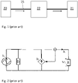
- Fig. 1 shows the working principle of an active filter.
- a load device 21 has a DC bus 15 for conducting the DC main currents.
- a source device 20 connected to the DC bus 15 with the load device 21 creates noise, in particular EMI.
- the noise flows on the DC bus 15 in the load device 21 as shown with the solid arrows. Although not shown, the noise flows back to the source device 20 over a ground connection.
- An active filter 22 between the source device 20 and the load device 21 creates a cancelling noise and injects the cancelling noise in the DC bus 15 to cancel the noise from the source device 20. Consequently, the noise is cancelled by the cancelling noise between the active filter 22 and the load device 21.
- the cancelling noise flows from the active filter 22 to the load device 21 and then over the ground connection back to the active filter 22.
- Fig. 2 shows a simple active filter circuit representation implemented as a feedback current-sensing current-injecting circuit, whereby the active filter measures a noise current and injects a cancelling noise current.
- the source impedance Zs and the load impedance Z L must be known.
- the source and load impedances Z S , Z L should have the same magnitude ratio over frequency. In this case, the source impedance Z S should be greater than the load impedance Z L .
- An aim of the present invention is the provision of an EMI filter that overcomes the shortcomings and limitations of the state of the art.
- the present disclosure concerns an EMI filter destined to cooperate with a DC network comprising a source device powering a load device via a DC bus.
- the EMI filter is connected at an input to the source device and at an output to the load device.
- the EMI filter comprises an active filter circuit having an active filter bandwidth and being configured to sense a noise component superimposed in the DC bus and inject a cancelling noise in the DC bus to suppress said noise component.
- the EMI filter further comprises a passive circuit including a source circuit connected at the input and a passive load circuit connected at the output, the passive circuit being configured to provide, at each frequency of the active filter bandwidth, a source impedance at the input that differs from a load impedance at the output by a factor of at least ten times.
- the passive source circuit is further configured to adjust the magnitude of the noise component such as to avoid saturation of the active filter circuit.
- the EMI filer disclosed herein provides a minimum, or maximum, impedance magnitude at every working frequency of the active filter bandwidth, so that the desired performance is achieved.
- the EMI filer guarantees proper functionality of the electronic circuit, without saturation of the circuit and/or instability.
- the EMI filer can function in different DC networks, without the need of being fine-tuned to each single application, i.e., different converters or different setups having unknown source and load impedances.
- the EMI filer can further avoid the saturation of the active filter electronic circuit.
- the EMI filer guarantees a stable and desired values of the source and load impedances, assuring the stability of the EMI filter and increase the performance in the working frequency band.
- an EMI filter 22 is shown according to an embodiment.
- the EMI filter 23 is destined to cooperate with a DC network comprising a source device 20 powering a load device 21 via a DC bus 15.
- the EMI filter 22 is connected to the source device 20 at an input 23.
- the term “input” substantially means “at the side of the source device 20”.
- the EMI filter 22 is further connected to the load device 21 at an output 24.
- the term “output” substantially means "at the side of the load device 21".
- the EMI filter 22 comprises an active filter circuit 220 having an active filter bandwidth and configured to sense a noise component superimposed in the DC bus 15 and inject a cancelling noise in the DC bus 15 to suppress said noise component.
- the EMI filter 22 further comprises a passive circuit including a passive source circuit 221 connected at the input 23 and a passive load circuit 222 connected at the output 24.
- the passive circuit is configured to provide, at each working frequency F W of the active filter bandwidth, a source impedance Z S at the input 23 that differs from a load impedance Z L at the output 24 by a factor of at least ten times.
- the active filter bandwidth is between 10 kHz and 10 MHz.
- the passive source circuit 221 can be further configured to adjust the magnitude of the noise component such as to avoid saturation of the active filter circuit 220.
- the passive source circuit 221 is configured to adjust the magnitude of the noise component below 300 mA. More generally, knowing the noise disturbance coming from the source device 20 and the maximum current/voltage capabilities of the active filter circuit 220, the passive source circuit 221 can be configured to adjust the current/voltage compensation capabilities of the active filter circuit 220, in other words, such that the noise disturbance is reduced in amplitude to fulfil the maximum capabilities of the active filter circuit 220. For example, the passive source circuit 221 can be configured to adjust the magnitude of the noise component by a factor of at least five times. In particular, if the noise coming from the source device 20 has current peaks of 5 A and the active filter circuit 220 can source/sink maximum 1 A, the passive source circuit 221 is designed to reduce the current peaks at least to 1 A.
- the active filter circuit 220 comprises a current-sensing current-injecting active filter.
- the passive circuit 221, 222 is configured such that, at each working frequency F W of the active filter bandwidth, the source impedance Z S is at least 10 times greater than the load impedance Z L .
- the passive source circuit 221 can include a n-order passive filter, wherein n is 2 or greater.
- Fig. 4 illustrates a possible configuration of the passive circuit including the source circuit 221 connected at the input 23 and the passive load circuit 222 connected at the output 24, according to an embodiment.
- the passive source circuit 221 can comprise a L-C circuit including at least a source capacitance C S , a source inductance L S and a source damping resistor R s .
- the passive source circuit 221 can comprise a L-C circuit including at least a source capacitance C S , a source inductance L S and a source damping resistor R s connected to the DC bus 15.
- the DC bus 15 can comprise a first power conductor 11 and a second power conductor 12.
- the L-C circuit including at least a source capacitance C S , a source inductance L S and a source damping resistor R s can be connected to each of the first and second power conductors 11, 12.
- the source damping resistor R s is equal or smaller than 3 ⁇ .
- the passive source circuit 221 can comprise a source capacitance C S of about 1 nF and a source inductance L S of about 7 ⁇ H.
- the passive load circuit 222 can include at least a single passive component C L , L L and a load damping resistor R L .
- the passive load circuit 222 can include at least a single passive component C L , L L and a load damping resistor R L connected to the DC bus 15.
- the DC bus 15 can comprise a first power conductor 11 and a second power conductor 12. In such configuration, the passive load circuit 222 can be connected to each of the first and second power conductors 11, 12.
- the passive load circuit 222 can include at a load capacitance C L of about 20 nF and a load damping resistor R L of about 1 ⁇ .
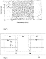
- Fig. 5 shows a graph of the source impedance Z S and the load impedance Z L plotted as a function of the working frequency F W of the active filter circuit 220 of Fig. 4 .
- the active filter bandwidth is indicated by the grey area on the graph.
- the active filter circuit 220 comprises a voltage-sensing voltage-injecting active filter.
- the passive load circuit 222 can be configured such that, at each frequency of the active filter bandwidth, a load impedance Z L is at least 10 times greater than the source impedance Zs.
- Fig. 6 schematically shows an example of such an active filter circuit 220 comprising a voltage-sensing voltage-injecting active filter including a passive source circuit 221 connected at the input 23 and a passive load circuit 222 connected at the output 24.
- the general description of the circuit is the same as for the current-sensing current-injecting of Fig. 4 , i.e., a second or higher order filter at source side and a single component filter at load side.
- the passive source circuit 221 can comprise a L-C circuit including a source capacitance C S (for example being about 3.3 uF), a source inductance L S (for example being about 100 nH) and a damping resistor R s smaller than 1 Ohm.
- the passive load circuit 222 can include a single inductance, e.g., 30 uH.
- the configuration of the EMI filter 22 shown in Fig. 6 allows for achieving load impedance Z L is at least 10 times greater than the source impedance Z S . in the working frequency of the active filter, i.e., 10 kHz - 10 MHz.
- Fig. 7 shows a graph of the source impedance Z S and the load impedance Z L plotted as a function of the working frequency F W of the active filter circuit 220 of Fig. 6 .
- the passive circuit 221, 222 is configured to provide, at each frequency of the active filter bandwidth, a source impedance Z S that differs from a load impedance Z L by a factor of at least ten times, and to adjust the magnitude of the noise component such as to avoid saturation of the active filter circuit 220, regardless of the configuration of the active filter 220.
- the active filter 220 can comprises a current-sensing current-injecting active filter, a voltage-sensing current-injecting active filter, a current-sensing voltage-injecting or a voltage-sensing voltage-injecting active filter.
- At least one capacitance can be provided between the first and second power conductors 11, 12 between the source device 20 and the EMI filter 22, such as to equalize the impedance seen from each power conductors 11, 12 to ground.
- a capacitance C 2 is added between the two power conductors 11, 12 on the side of the passive source circuit 221.
- the passive source circuit 221 and the passive load circuit 222 are similar to the ones shown in Fig. 4 .
- the EMI filter 22 can be placed in a motor drive unit on a DC power bus, in an electric vehicle, although this is not the only application of the present disclosure.
- Other applications of the EMI filter 22 can include input or output of DC/DC converters and on-board chargers, for example in a vehicle.
Landscapes
- Engineering & Computer Science (AREA)
- Power Engineering (AREA)
- Physics & Mathematics (AREA)
- Electromagnetism (AREA)
- Filters And Equalizers (AREA)
- Networks Using Active Elements (AREA)
Abstract
Electromagnetic compatibility (EMI) filter (22) comprising a source device (20) powering a load device (21) via a DC bus (15); the EMI filter (22) being connected at an input (23) to the source device (20) and at an output (24) to the load device (21); the EMI filter (22) comprising an active filter circuit (220) having an active filter bandwidth and being configured to sense a noise component superimposed in the DC bus (15) and inject a cancelling noise in the DC bus (15) to suppress said noise component. The EMI filter (22) comprises a passive circuit including a source circuit (221) connected at the input (23) and a passive load circuit (222) connected at the output (24), the passive circuit being configured to provide, at each frequency of the active filter bandwidth, a source impedance (Zs) at the input (23) that differs from a load impedance (Z<sub>L</sub>) at the output (24) by a factor of at least ten times.
Description
- The present disclosure concerns an electromagnetic compatibility filter for suppressing an unwanted electromagnetic noise component superimposed on an electric supply line. In particular, the present invention concerns an active electromagnetic noise interference (EMI) filter having enhanced performances.
- Electric systems in vehicles and in industry are becoming ever more complex and include a multitude of components that generate, or are liable to be disturbed by, electromagnetic interferences. Electric motors, for example, are often driven by electronic inverters that control the motor speed and torque by generating waveforms with variable frequency and amplitude. These systems provide high efficiency but generate a powerful electromagnetic noise.
- Switching power converters are used in electric and hybrid vehicles, as well as in countless other applications such as driving stationary motors, battery chargers, photovoltaic systems, lighting control, computers, and other. In all these cases, the switching action of the converter is a source of electromagnetic noise that could, if it is not managed or attenuated, affect the functioning of other systems, or exceed normative limits.
- Electric or electronic filters used to attenuate these unwanted electromagnetic interferences, called EMI filters in short, are used in all branches of electric engineering to improve reliability and respect existing norms. Well-designed filtering system are essential to the performance of many complex electric systems.
- Electric and hybrid vehicles are equipped with different power converters in a very tight space. This coexistence represents a serious electromagnetic problem and demands efficient EMI filtering. When the filters ae not enough to bring the noise to acceptable levels, shielded cables can be used, but they contribute significantly to costs.
- It is known to use passive low-pass LC filters to attenuate EMI. While passive solutions do offer substantial attenuation, they have their limits. Magnetic components rated for the current levels used in modern electric vehicles are bulky, expensive, heavy, and not always suitable for mass production.
- Document
US20180269781 discloses an active EMI filter for an electric vehicle. Active filters can be more compact than equivalent passive ones but providing a satisfactory active filter for the high-current wide-bandwidth interferences generated in electric vehicles is difficult. -
Fig. 1 shows the working principle of an active filter. Aload device 21 has aDC bus 15 for conducting the DC main currents. Asource device 20 connected to theDC bus 15 with theload device 21 creates noise, in particular EMI. The noise flows on theDC bus 15 in theload device 21 as shown with the solid arrows. Although not shown, the noise flows back to thesource device 20 over a ground connection. Anactive filter 22 between thesource device 20 and theload device 21 creates a cancelling noise and injects the cancelling noise in theDC bus 15 to cancel the noise from thesource device 20. Consequently, the noise is cancelled by the cancelling noise between theactive filter 22 and theload device 21. The cancelling noise flows from theactive filter 22 to theload device 21 and then over the ground connection back to theactive filter 22. -
Fig. 2 shows a simple active filter circuit representation implemented as a feedback current-sensing current-injecting circuit, whereby the active filter measures a noise current and injects a cancelling noise current. For the proper functionality, performance and stability of an active filter, the source impedance Zs and the load impedance ZL must be known. - The performance, i.e., the attenuation of a feedback current-sensing current-injecting active filter (called insertion loss, IL), is given by Equation 1:

- Since in a real active filter circuit it is not always possible to know or measure exactly the source and load impedances ZS, ZL in the working frequency F W range of the active filter, there is a need to control the source and load impedance ZS, ZL such as to guarantee a stable operation of the active filter. To maximize the attenuation of the feedback current-sensing current-injecting active filter, the source and load impedances ZS, ZL should have the same magnitude ratio over frequency. In this case, the source impedance ZS should be greater than the load impedance ZL.
- For a voltage-sensing voltage-injecting circuit configuration of the active filter, insertion Loss, IL is given by Equation 2:

- An aim of the present invention is the provision of an EMI filter that overcomes the shortcomings and limitations of the state of the art.
- The present disclosure concerns an EMI filter destined to cooperate with a DC network comprising a source device powering a load device via a DC bus. The EMI filter is connected at an input to the source device and at an output to the load device. The EMI filter comprises an active filter circuit having an active filter bandwidth and being configured to sense a noise component superimposed in the DC bus and inject a cancelling noise in the DC bus to suppress said noise component. The EMI filter further comprises a passive circuit including a source circuit connected at the input and a passive load circuit connected at the output, the passive circuit being configured to provide, at each frequency of the active filter bandwidth, a source impedance at the input that differs from a load impedance at the output by a factor of at least ten times. The passive source circuit is further configured to adjust the magnitude of the noise component such as to avoid saturation of the active filter circuit.
- The EMI filer disclosed herein provides a minimum, or maximum, impedance magnitude at every working frequency of the active filter bandwidth, so that the desired performance is achieved. The EMI filer guarantees proper functionality of the electronic circuit, without saturation of the circuit and/or instability.
- The EMI filer can function in different DC networks, without the need of being fine-tuned to each single application, i.e., different converters or different setups having unknown source and load impedances.
- The EMI filer can further avoid the saturation of the active filter electronic circuit. The EMI filer guarantees a stable and desired values of the source and load impedances, assuring the stability of the EMI filter and increase the performance in the working frequency band.
- Exemplar embodiments of the invention are disclosed in the description and illustrated by the drawings in which:
-
Fig. 1 shows the working principle of an active filter; -
Fig. 2 shows an active filter circuit representation implemented as a feedback current-sensing current-injecting circuit; -
Fig. 3 illustrates an EMI filter comprising a passive circuit, according to an embodiment; -
Fig. 4 illustrates a possible configuration of the passive circuit, according to an embodiment; -
Fig. 5 shows a graph of the source impedance and the load impedance plotted as a function of the working frequency of the active filter circuit ofFig. 4 ; -
Fig. 6 illustrates a possible configuration of the passive circuit, according to another embodiment; -
Fig. 7 shows a graph of the source impedance and the load impedance plotted as a function of the working frequency of the active filter circuit ofFig. 6 ; and -
Fig. 8 illustrates the EMI filter, according to another embodiment. - With reference to
Fig. 3 , anEMI filter 22 is shown according to an embodiment. TheEMI filter 23 is destined to cooperate with a DC network comprising asource device 20 powering aload device 21 via aDC bus 15. TheEMI filter 22 is connected to thesource device 20 at aninput 23. Here, the term "input" substantially means "at the side of thesource device 20". TheEMI filter 22 is further connected to theload device 21 at anoutput 24. Here, the term "output" substantially means "at the side of theload device 21". TheEMI filter 22 comprises anactive filter circuit 220 having an active filter bandwidth and configured to sense a noise component superimposed in theDC bus 15 and inject a cancelling noise in theDC bus 15 to suppress said noise component. - The
EMI filter 22 further comprises a passive circuit including apassive source circuit 221 connected at theinput 23 and apassive load circuit 222 connected at theoutput 24. The passive circuit is configured to provide, at each working frequency F W of the active filter bandwidth, a source impedance ZS at theinput 23 that differs from a load impedance Z L at theoutput 24 by a factor of at least ten times. - The active filter bandwidth is between 10 kHz and 10 MHz.
- The
passive source circuit 221 can be further configured to adjust the magnitude of the noise component such as to avoid saturation of theactive filter circuit 220. - In one aspect, the
passive source circuit 221 is configured to adjust the magnitude of the noise component below 300 mA. More generally, knowing the noise disturbance coming from thesource device 20 and the maximum current/voltage capabilities of theactive filter circuit 220, thepassive source circuit 221 can be configured to adjust the current/voltage compensation capabilities of theactive filter circuit 220, in other words, such that the noise disturbance is reduced in amplitude to fulfil the maximum capabilities of theactive filter circuit 220. For example, thepassive source circuit 221 can be configured to adjust the magnitude of the noise component by a factor of at least five times. In particular, if the noise coming from thesource device 20 has current peaks of 5 A and theactive filter circuit 220 can source/sink maximum 1 A, thepassive source circuit 221 is designed to reduce the current peaks at least to 1 A. - In an embodiment, the
active filter circuit 220 comprises a current-sensing current-injecting active filter. Thepassive circuit - In one aspect, the
passive source circuit 221 can include a n-order passive filter, wherein n is 2 or greater. -
Fig. 4 illustrates a possible configuration of the passive circuit including thesource circuit 221 connected at theinput 23 and thepassive load circuit 222 connected at theoutput 24, according to an embodiment. As shown ifFig. 4 , thepassive source circuit 221 can comprise a L-C circuit including at least a source capacitance CS, a source inductance LS and a source damping resistor Rs. For example, thepassive source circuit 221 can comprise a L-C circuit including at least a source capacitance CS, a source inductance LS and a source damping resistor Rs connected to theDC bus 15. - As shown in
Fig. 4 , theDC bus 15 can comprise afirst power conductor 11 and asecond power conductor 12. In such configuration, the L-C circuit including at least a source capacitance CS, a source inductance LS and a source damping resistor Rs can be connected to each of the first andsecond power conductors - In one aspect, the source damping resistor Rs is equal or smaller than 3 Ω.
- In one aspect, the
passive source circuit 221 can comprise a source capacitance CS of about 1 nF and a source inductance LS of about 7 µH. - The
passive load circuit 222 can include at least a single passive component CL, LL and a load damping resistor RL. For example, thepassive load circuit 222 can include at least a single passive component CL, LL and a load damping resistor RL connected to theDC bus 15. As shown inFig. 4 , theDC bus 15 can comprise afirst power conductor 11 and asecond power conductor 12. In such configuration, thepassive load circuit 222 can be connected to each of the first andsecond power conductors - In one aspect, the
passive load circuit 222 can include at a load capacitance CL of about 20 nF and a load damping resistor RL of about 1 Ω. -
Fig. 5 shows a graph of the source impedance ZS and the load impedance Z L plotted as a function of the working frequency F W of theactive filter circuit 220 ofFig. 4 . The active filter bandwidth is indicated by the grey area on the graph. - In another embodiment, the
active filter circuit 220 comprises a voltage-sensing voltage-injecting active filter. Thepassive load circuit 222 can be configured such that, at each frequency of the active filter bandwidth, a load impedance Z L is at least 10 times greater than the source impedance Zs. -
Fig. 6 schematically shows an example of such anactive filter circuit 220 comprising a voltage-sensing voltage-injecting active filter including apassive source circuit 221 connected at theinput 23 and apassive load circuit 222 connected at theoutput 24. The general description of the circuit is the same as for the current-sensing current-injecting ofFig. 4 , i.e., a second or higher order filter at source side and a single component filter at load side. For example, thepassive source circuit 221 can comprise a L-C circuit including a source capacitance CS (for example being about 3.3 uF), a source inductance LS (for example being about 100 nH) and a damping resistor Rs smaller than 1 Ohm. Thepassive load circuit 222 can include a single inductance, e.g., 30 uH. The configuration of theEMI filter 22 shown inFig. 6 allows for achieving load impedance Z L is at least 10 times greater than the source impedance Z S. in the working frequency of the active filter, i.e., 10 kHz - 10 MHz. -
Fig. 7 shows a graph of the source impedance Z S and the load impedance Z L plotted as a function of the working frequency F W of theactive filter circuit 220 ofFig. 6 . - The
passive circuit active filter circuit 220, regardless of the configuration of theactive filter 220. For example, theactive filter 220 can comprises a current-sensing current-injecting active filter, a voltage-sensing current-injecting active filter, a current-sensing voltage-injecting or a voltage-sensing voltage-injecting active filter. - In yet another embodiment, at least one capacitance can be provided between the first and
second power conductors source device 20 and theEMI filter 22, such as to equalize the impedance seen from eachpower conductors EMI filter 22 illustrated inFig. 8 , a capacitance C2 is added between the twopower conductors passive source circuit 221. Here, thepassive source circuit 221 and thepassive load circuit 222 are similar to the ones shown inFig. 4 . - The
EMI filter 22 can be placed in a motor drive unit on a DC power bus, in an electric vehicle, although this is not the only application of the present disclosure. Other applications of theEMI filter 22 can include input or output of DC/DC converters and on-board chargers, for example in a vehicle. -
- 11
- first power conductor
- 12
- second power conductor
- 15
- DC bus
- 20
- source device
- 21
- load device
- 22
- electromagnetic compatibility (EMI) filter
- 220
- active filter circuit
- 221
- passive source circuit
- 222
- passive load circuit
- 223
- passive circuit
- 23
- input
- 24
- output
- A
- filter gain
- BF
- active filter bandwidth
- CL
- load capacitance
- CS
- source capacitance
- C2
- capacitance
- FW
- working frequency
- IL
- insertion Loss
- LL
- load inductance
- LS
- source inductance
- RL
- load damping resistor
- RS
- source damping resistor
- ZS
- source impedance
- ZL
- load impedance
Claims (12)
- Electromagnetic compatibility (EMI) filter (22) destined to cooperate with a DC network comprising a source device (20) powering a load device (21) via a DC bus (15);
the EMI filter (22) being connected at an input (23) to the source device (20) and at an output (24) to the load device (21);
the EMI filter (22) comprising an active filter circuit (220) having an active filter bandwidth and being configured to sense a noise component superimposed in the DC bus (15) and inject a cancelling noise in the DC bus (15) to suppress said noise component;
characterized in that the EMI filter (22) further comprises a passive circuit including a source circuit (221) connected at the input (23) and a passive load circuit (222) connected at the output (24), the passive circuit being configured to provide, at each frequency of the active filter bandwidth, a source impedance (Zs) at the input (23) that differs from a load impedance (Z L) at the output (24) by a factor of at least ten times; and
in that the passive source circuit (221) is further configured to adjust the magnitude of the noise component such as to avoid saturation of the active filter circuit (220). - The EMI filter, according to claim 1,
wherein the passive source circuit (221) includes a n-order passive filter; and wherein n is 2 or greater. - The EMI filter, according to claim 2,
wherein the passive source circuit (221) comprises a L-C circuit including at least a source capacitance (CS), a source inductance (LS) and a source damping resistor (RS). - The EMI filter, according to claim 3,
wherein the source damping resistor (RS) is equal or smaller than 3 Ω. - The EMI filter, according to any one of claims 1 to 4,
wherein the passive load circuit (222) includes at least a single passive component (CL, LL) and a load damping resistor (RL). - The EMI filter, according to any one of claims 1 to 5,
wherein the active filter circuit (220) is a current-sensing current-injecting active filter; and
wherein the passive circuit (221, 222) is configured such that, at each frequency of the active filter bandwidth, the source impedance (Z S) is at least 10 times greater than the load impedance (Z L). - The EMI filter, according to claims 3 and 6,
wherein the passive source circuit (221) comprises a source capacitance (CS) of about 1 nF and a source inductance (LS) of about 7 µH. - The EMI filter, according to any one of claims 4 to 7,
wherein the active filter circuit (220) is a voltage-sensing voltage-injecting active filter; and
wherein the passive circuit (221, 222) is configured such that, at each frequency of the active filter bandwidth, the load impedance (Z L) is at least 10 times greater than the source impedance (Z S). - The EMI filter, according to claims 5 and 8,
wherein the passive load circuit (222) includes at a load capacitance (CL) of about 20 nF and a load damping resistor (RL) of about 1 Ω. - The EMI filter, according to any one of claims 1 to 9,
wherein the active filter bandwidth is between 10 kHz and 10 MHz. - The EMI filter, according to any one of claims 1 to 10,
wherein the passive source circuit (221) is configured to adjust the current/voltage compensation capabilities of the active filter circuit (220). - The EMI filter, according to any one of claims 1 to 11,
wherein the DC bus (15) comprises a first power conductor (11) and a second power conductor (12); and
wherein at least one capacitance (C2) is provided between the first and second power conductors (11, 12) between the source device (20) and the EMI filter (22), such as to equalize the impedance seen from each power conductors (11, 12) to ground.
Priority Applications (5)
| Application Number | Priority Date | Filing Date | Title |
|---|---|---|---|
| EP21157900.8A EP4047768A1 (en) | 2021-02-18 | 2021-02-18 | Electromagnetic compatibility filter having controlled impedance magnitude |
| JP2022010257A JP7506699B2 (en) | 2021-02-18 | 2022-01-26 | Electromagnetic interference filters that control the magnitude of impedance |
| US17/670,311 US12294346B2 (en) | 2021-02-18 | 2022-02-11 | Electromagnetic interference filter having controlled impedance magnitude |
| EP22156967.6A EP4047769A1 (en) | 2021-02-18 | 2022-02-16 | Electromagnetic interference filter having controlled impedance magnitude |
| CN202210146252.XA CN114977772A (en) | 2021-02-18 | 2022-02-17 | Electromagnetic interference filter with controlled impedance magnitude |
Applications Claiming Priority (1)
| Application Number | Priority Date | Filing Date | Title |
|---|---|---|---|
| EP21157900.8A EP4047768A1 (en) | 2021-02-18 | 2021-02-18 | Electromagnetic compatibility filter having controlled impedance magnitude |
Publications (1)
| Publication Number | Publication Date |
|---|---|
| EP4047768A1 true EP4047768A1 (en) | 2022-08-24 |
Family
ID=74668723
Family Applications (2)
| Application Number | Title | Priority Date | Filing Date |
|---|---|---|---|
| EP21157900.8A Withdrawn EP4047768A1 (en) | 2021-02-18 | 2021-02-18 | Electromagnetic compatibility filter having controlled impedance magnitude |
| EP22156967.6A Pending EP4047769A1 (en) | 2021-02-18 | 2022-02-16 | Electromagnetic interference filter having controlled impedance magnitude |
Family Applications After (1)
| Application Number | Title | Priority Date | Filing Date |
|---|---|---|---|
| EP22156967.6A Pending EP4047769A1 (en) | 2021-02-18 | 2022-02-16 | Electromagnetic interference filter having controlled impedance magnitude |
Country Status (4)
| Country | Link |
|---|---|
| US (1) | US12294346B2 (en) |
| EP (2) | EP4047768A1 (en) |
| JP (1) | JP7506699B2 (en) |
| CN (1) | CN114977772A (en) |
Citations (3)
| Publication number | Priority date | Publication date | Assignee | Title |
|---|---|---|---|---|
| US20140312966A1 (en) * | 2013-04-19 | 2014-10-23 | Schaffner Emv Ag | Active emc filter |
| US20180269781A1 (en) | 2017-03-17 | 2018-09-20 | Schaffner Emv Ag | Active filter |
| US20200044625A1 (en) * | 2017-02-09 | 2020-02-06 | Avl Software And Functions Gmbh | Active Filter for Bipolar Voltage Sources |
Family Cites Families (13)
| Publication number | Priority date | Publication date | Assignee | Title |
|---|---|---|---|---|
| JP2863833B2 (en) * | 1996-09-18 | 1999-03-03 | 岡山大学長 | Active common mode canceller |
| JP3822910B2 (en) * | 1997-06-19 | 2006-09-20 | ウィスコンシン アラムニ リサーチ ファンデーション | Reduction of power line harmonics by hybrid parallel active / passive filter system with square wave inverter and DC bus control |
| US7595687B2 (en) * | 2006-07-31 | 2009-09-29 | Wisconsin Alumni Research Foundation | Apparatus and method for reducing EMI generated by a power conversion device |
| KR101039310B1 (en) * | 2008-05-02 | 2011-06-08 | 한국수자원공사 | Complex Active Power Filter |
| JP5454001B2 (en) | 2009-08-21 | 2014-03-26 | 株式会社デンソー | Current suppressor |
| JP5248713B2 (en) | 2010-08-26 | 2013-07-31 | 三菱電機株式会社 | Leakage current reduction device |
| US8461774B2 (en) | 2011-03-15 | 2013-06-11 | General Electric Company | Lighting power circuit with peak current limiter for EMI filter |
| JP5993886B2 (en) | 2014-03-04 | 2016-09-14 | 株式会社豊田中央研究所 | Noise filter |
| CN110168898B (en) | 2016-12-12 | 2021-04-09 | 三菱电机株式会社 | Power conversion device |
| US10374510B2 (en) * | 2017-04-07 | 2019-08-06 | Texas Instruments Incorporated | Compensated active electro-magnetic interference filters |
| CN107230981A (en) * | 2017-07-07 | 2017-10-03 | 华中科技大学 | A kind of Series Hybrid Type Active Power Filters containing harmonic pad |
| CN108051671B (en) * | 2017-12-08 | 2022-12-13 | 中国核动力研究设计院 | Device and method for inhibiting power line conduction emission in wide frequency range |
| US10784678B1 (en) * | 2018-01-26 | 2020-09-22 | Universal Lighting Technologies, Inc. | Damped PI-type filter Y-type capacitance network for radiated and conducted emission |
-
2021
- 2021-02-18 EP EP21157900.8A patent/EP4047768A1/en not_active Withdrawn
-
2022
- 2022-01-26 JP JP2022010257A patent/JP7506699B2/en active Active
- 2022-02-11 US US17/670,311 patent/US12294346B2/en active Active
- 2022-02-16 EP EP22156967.6A patent/EP4047769A1/en active Pending
- 2022-02-17 CN CN202210146252.XA patent/CN114977772A/en active Pending
Patent Citations (3)
| Publication number | Priority date | Publication date | Assignee | Title |
|---|---|---|---|---|
| US20140312966A1 (en) * | 2013-04-19 | 2014-10-23 | Schaffner Emv Ag | Active emc filter |
| US20200044625A1 (en) * | 2017-02-09 | 2020-02-06 | Avl Software And Functions Gmbh | Active Filter for Bipolar Voltage Sources |
| US20180269781A1 (en) | 2017-03-17 | 2018-09-20 | Schaffner Emv Ag | Active filter |
Non-Patent Citations (2)
| Title |
|---|
| AMADUCCI ALESSANDRO: "Design of a wide bandwidth active filter for common mode EMI suppression in automotive systems", 2017 IEEE INTERNATIONAL SYMPOSIUM ON ELECTROMAGNETIC COMPATIBILITY & SIGNAL/POWER INTEGRITY (EMCSI), IEEE, 7 August 2017 (2017-08-07), pages 612 - 618, XP033232510, ISBN: 978-1-5386-2229-2, [retrieved on 20171020], DOI: 10.1109/ISEMC.2017.8077941 * |
| MARCELO LOBO HELDWEIN ET AL: "Implementation of a Transformerless Common-Mode Active Filter for Offline Converter Systems", IEEE TRANSACTIONS ON INDUSTRIAL ELECTRONICS, IEEE SERVICE CENTER, PISCATAWAY, NJ, USA, vol. 57, no. 5, 1 May 2010 (2010-05-01), pages 1772 - 1786, XP011295954, ISSN: 0278-0046 * |
Also Published As
| Publication number | Publication date |
|---|---|
| CN114977772A (en) | 2022-08-30 |
| JP2022126591A (en) | 2022-08-30 |
| US20220263486A1 (en) | 2022-08-18 |
| JP7506699B2 (en) | 2024-06-26 |
| US12294346B2 (en) | 2025-05-06 |
| EP4047769A1 (en) | 2022-08-24 |
Similar Documents
| Publication | Publication Date | Title |
|---|---|---|
| CN102332808B (en) | Comprise the inverter filtering device of differential mode and common mode and comprise the system of this inverter filtering device | |
| RU2508589C2 (en) | Resonance suppression system and method | |
| EP4315545B1 (en) | Electromagnetic interference filter | |
| EP3255770A1 (en) | Filter and power supply system | |
| US10700591B2 (en) | Voltage converter, electric drive system and method for reducing interference voltages | |
| EP2940701B1 (en) | Hybrid planar common-mode choke | |
| US11251693B2 (en) | Electrical filter device for filtering a common-mode interference between a current source and a load | |
| US10910944B2 (en) | Voltage converter, electric drive system and method for reducing interference voltages | |
| EP4047769A1 (en) | Electromagnetic interference filter having controlled impedance magnitude | |
| US12341483B2 (en) | Multistage active filter for automotive applications | |
| EP4047803B1 (en) | High-frequency current source for an active emi filter, active emi filter and use of an active emi filter | |
| EP4075669A1 (en) | High frequency, high output impedance amplifier for emi active filter applications | |
| EP3800772B1 (en) | Damper for power train | |
| US8963366B2 (en) | System for power transmission | |
| EP4637015A1 (en) | Power converter with active filter circuit | |
| EP3817206A1 (en) | Output filter for power train | |
| CN117394674A (en) | Electromagnetic interference filter and electronic equipment | |
| JP2026052346A (en) | Common mode noise filter | |
| JP2009232161A (en) | Voltage oscillation reducing filter and inverter using the same | |
| Weber et al. | Efficient EMI-Filters for High-Current Mobile Applications |
Legal Events
| Date | Code | Title | Description |
|---|---|---|---|
| PUAI | Public reference made under article 153(3) epc to a published international application that has entered the european phase |
Free format text: ORIGINAL CODE: 0009012 |
|
| STAA | Information on the status of an ep patent application or granted ep patent |
Free format text: STATUS: THE APPLICATION HAS BEEN PUBLISHED |
|
| AK | Designated contracting states |
Kind code of ref document: A1 Designated state(s): AL AT BE BG CH CY CZ DE DK EE ES FI FR GB GR HR HU IE IS IT LI LT LU LV MC MK MT NL NO PL PT RO RS SE SI SK SM TR |
|
| STAA | Information on the status of an ep patent application or granted ep patent |
Free format text: STATUS: THE APPLICATION IS DEEMED TO BE WITHDRAWN |
|
| 18D | Application deemed to be withdrawn |
Effective date: 20230629 |