EP4047743B1 - Vehicle with optimized system for transceiving data - Google Patents
Vehicle with optimized system for transceiving data Download PDFInfo
- Publication number
- EP4047743B1 EP4047743B1 EP22157411.4A EP22157411A EP4047743B1 EP 4047743 B1 EP4047743 B1 EP 4047743B1 EP 22157411 A EP22157411 A EP 22157411A EP 4047743 B1 EP4047743 B1 EP 4047743B1
- Authority
- EP
- European Patent Office
- Prior art keywords
- vehicle
- antennas
- millimeter
- antenna
- wave
- Prior art date
- Legal status (The legal status is an assumption and is not a legal conclusion. Google has not performed a legal analysis and makes no representation as to the accuracy of the status listed.)
- Active
Links
Images






Classifications
-
- H—ELECTRICITY
- H01—ELECTRIC ELEMENTS
- H01Q—ANTENNAS, i.e. RADIO AERIALS
- H01Q1/00—Details of, or arrangements associated with, antennas
- H01Q1/27—Adaptation for use in or on movable bodies
- H01Q1/32—Adaptation for use in or on road or rail vehicles
- H01Q1/3208—Adaptation for use in or on road or rail vehicles characterised by the application wherein the antenna is used
-
- H—ELECTRICITY
- H01—ELECTRIC ELEMENTS
- H01Q—ANTENNAS, i.e. RADIO AERIALS
- H01Q1/00—Details of, or arrangements associated with, antennas
- H01Q1/27—Adaptation for use in or on movable bodies
- H01Q1/32—Adaptation for use in or on road or rail vehicles
- H01Q1/325—Adaptation for use in or on road or rail vehicles characterised by the location of the antenna on the vehicle
- H01Q1/3283—Adaptation for use in or on road or rail vehicles characterised by the location of the antenna on the vehicle side-mounted antennas, e.g. bumper-mounted, door-mounted
-
- H—ELECTRICITY
- H01—ELECTRIC ELEMENTS
- H01Q—ANTENNAS, i.e. RADIO AERIALS
- H01Q19/00—Combinations of primary active antenna elements and units with secondary devices, e.g. with quasi-optical devices, for giving the antenna a desired directional characteristic
- H01Q19/005—Patch antenna using one or more coplanar parasitic elements
-
- H—ELECTRICITY
- H01—ELECTRIC ELEMENTS
- H01Q—ANTENNAS, i.e. RADIO AERIALS
- H01Q21/00—Antenna arrays or systems
- H01Q21/06—Arrays of individually energised antenna units similarly polarised and spaced apart
- H01Q21/061—Two dimensional planar arrays
- H01Q21/065—Patch antenna array
-
- H—ELECTRICITY
- H01—ELECTRIC ELEMENTS
- H01Q—ANTENNAS, i.e. RADIO AERIALS
- H01Q21/00—Antenna arrays or systems
- H01Q21/06—Arrays of individually energised antenna units similarly polarised and spaced apart
- H01Q21/20—Arrays of individually energised antenna units similarly polarised and spaced apart the units being spaced along or adjacent to a curvilinear path
- H01Q21/205—Arrays of individually energised antenna units similarly polarised and spaced apart the units being spaced along or adjacent to a curvilinear path providing an omnidirectional coverage
-
- H—ELECTRICITY
- H01—ELECTRIC ELEMENTS
- H01Q—ANTENNAS, i.e. RADIO AERIALS
- H01Q21/00—Antenna arrays or systems
- H01Q21/28—Combinations of substantially independent non-interacting antenna units or systems
-
- H—ELECTRICITY
- H01—ELECTRIC ELEMENTS
- H01Q—ANTENNAS, i.e. RADIO AERIALS
- H01Q5/00—Arrangements for simultaneous operation of antennas on two or more different wavebands, e.g. dual-band or multi-band arrangements
- H01Q5/30—Arrangements for providing operation on different wavebands
-
- H—ELECTRICITY
- H01—ELECTRIC ELEMENTS
- H01Q—ANTENNAS, i.e. RADIO AERIALS
- H01Q9/00—Electrically-short antennas having dimensions not more than twice the operating wavelength and consisting of conductive active radiating elements
- H01Q9/04—Resonant antennas
- H01Q9/0407—Substantially flat resonant element parallel to ground plane, e.g. patch antenna
- H01Q9/045—Substantially flat resonant element parallel to ground plane, e.g. patch antenna with particular feeding means
- H01Q9/0457—Substantially flat resonant element parallel to ground plane, e.g. patch antenna with particular feeding means electromagnetically coupled to the feed line
Definitions
- the present invention relates to a vehicle, in particular a road vehicle, comprising a system that is optimized for transceiving data and configured in particular to operate in the 5G frequency band.
- mmW millimeter-wave
- antennas which are usually subject to problems related to the attenuation of signals due to propagation in free spaces or the presence of obstacles.
- US 2020/185819 A1 discloses an antenna system which is installed on a vehicle and comprises a first antenna system having a plurality of first antenna elements disposed within a structure mounted in the vehicle, to perform Multi Input Multi Output (MIMO), and a second antenna system having a plurality of second antenna elements attached to side surfaces of a polyhedron disposed within the structure, to perform beamforming.
- MIMO Multi Input Multi Output
- US 2018/288672 A1 discloses a vehicle-mounted millimeter-wave communication device which includes an acquisition unit for acquiring a relay request that requests relay of communication from a first communication partner, a detection unit for detecting directions of the first communication partner and a second communication partner that are viewed from the vehicle, and a communication control unit for performing control such that, in the case where the relay request is received from the first communication partner and it is possible to communicate with the second communication partner, communication, in which a communication time longer than a communication time set for another direction is set for each of the directions of the first communication partner and the second communication partner, is performed, and communication between the first communication partner and the second communication partner is relayed.
- EP 1612954 A2 discloses a vehicle which has a transmitting/receiving component for transmitting information, operation data and/or commands to a nearby vehicle or to nearby compartment of same vehicle, wherein the component operates at range of 20-70 Giga hertz.
- the component that is designed as a high frequency radio antenna is integrated into a lens and/or clear-view screen of a frontal illumination device and/or signal device.
- DE 102013021819 A1 discloses a radar device for a motor vehicle, with a vehicle light for illuminating the motor vehicle surroundings, and with a radar sensor for detecting target objects located in the surroundings.
- the radar sensor has an antenna unit that is arranged in a housing interior of the vehicle light, for emitting/receiving electromagnetic radar waves.
- a controller activates the antenna unit and is arranged outside the housing interior of the vehicle light.
- the radar sensor has a connecting unit via which the controller is electrically coupled to the antenna unit through a housing wall of the housing.
- WO 2021/133408 A1 representing a prior right under Article 54(3) EPC, discloses a vehicle having antennas elements which include antennas arrays that can support various communication technologies and can be integrated into different components or subcomponents of the vehicle.
- the main object of the present invention is to mitigate these problems, and in particular to offer a solution that makes it possible to find an appropriate balance between the requirement to adequately cover the signal transceiver field around the vehicle and the need for an optimized number of antennas.
- a vehicle in particular a road vehicle, such as an automobile, as defined in claim 1.
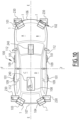
- FIG 10 schematically illustrates a vehicle according to the invention, indicated by the reference numeral 100, in which a system for transceiving data is installed on board the vehicle itself; an exemplary embodiment of this system for the transceiving of data is illustrated in Figure 9 and indicated therein by the overall reference numeral 200.
- the system 200 installed on board the vehicle 100 comprises at least one first set of millimeter-wave antennas 1 for the transceiving of data in the 5G frequency band, in particular with frequencies equal to or greater than 20 Ghz and up to 100 GHz, and in which, with respect to an imaginary first plane E and an imaginary second plane F that are perpendicular to each other and that virtually divide the vehicle 100 into four quadrants A, B, C, D, the said at least one first set of millimeter-wave antennas 1 comprises at least four antennas 1, which are each installed in a corresponding quadrant of the said four quadrants A, B, C, D, and an embodiment of which is illustrated in Figures 1-8 .
- these four quadrants A, B, C and D may be substantially identical to or different from each other, and the planes E and F are to be considered to be drawn, for example, in a manner such as to include the two corresponding direct centre-line axes one along the line joining front-rear of the vehicle, and the other along the line joining the lateral sides of the same.
- At least the two front quadrants A and B are to be considered identical to each other and the two rear quadrants C and D are also to be considered identical to each other.
- At least one of the four millimeter-wave antennas 1 used comprises at least one radiating element 14, and is arranged in the respective quadrant A, B, C, D in a manner so that between the at least one radiating element 14 and the surface external to the vehicle 100 towards which irradiation is to occur or from which signals are to be received, there are interposed one or more surfaces of non-metallic material and having a coefficient of loss (also referred to as dissipation factor "tan ⁇ " and equal to the ratio between the active power and reactive power absorbed by the material) lower than 0.1.
- a coefficient of loss also referred to as dissipation factor "tan ⁇ " and equal to the ratio between the active power and reactive power absorbed by the material
- a first antenna 1 is arranged to be coincident with a left front headlight 101 or left front headlight assembly 101 of the vehicle 100; a second antenna 1 is arranged to be coincident with a right front headlight 102 or right front headlight assembly 102 of the vehicle 100; a third antenna 1 is arranged to be coincident with a left rear taillight 103 or left rear taillight assembly 103 of the vehicle 100; and a fourth antenna 1 is arranged to be coincident with a right rear taillight 104 or right rear taillight assembly 104 of the vehicle 100.
- a first antenna 1 is arranged to be coincident with a side bumper 109 mounted on the left front door 112; a second antenna 1 is arranged to be coincident with a side bumper 109 mounted on the right front door; a third antenna 1 is arranged to be coincident with a side bumper 109 mounted on the left rear door 112; and a fourth antenna 1 is arranged to be coincident with a side bumper 109 mounted on the left front door 112.
- FIG. 1-8 A preferred embodiment of at least one of the millimeter-wave antennas 1 is illustrated in Figures 1-8 .
- the antenna 1 comprises a containment casing, schematically illustrated in Figure 1 by the reference numeral 2, which houses inside it all or at least part of the components of the antenna.
- This containment casing 2 is for example made of plastic material and is conveniently mounted integrated on the reflector of a corresponding front headlight or headlight assembly, or rear taillight or taillight assembly of the vehicle 100, for example as illustrated in Figure 11 for the right front headlight assembly 102.
- the antenna 1 may be substantially integrated into the structure of the associated head/taillight assembly, with its own containment casing 2 which is inserted in a suitable housing formed in the body of the reflector of the associated head/taillight or head/taillight assembly 101, 102, 103 and 104, in a manner such that its external surface, which faces the environment external to the vehicle 100, is substantially coplanar with the surface of the reflector itself.
- the antenna 1 can be substantially integrated into the structure of the associated side bumper 109, with its own containment casing 2 which is inserted in a suitable housing formed in the body of the bumper, for example in a manner such that its external surface, which faces the environment external to the vehicle 100, is substantially coplanar with the external surface of the side bumper itself.
- the four antennas 1 are connected, for the purposes and functionalities that will be described in detail below, to a first control unit 210 that is installed on the vehicle in a remote position distant from the antennas 1, and is connected to the antennas 1 by means of corresponding connection cables 211 which may be coaxial or digital type cables depending on the applications.
- each antenna 1 comprises, arranged inside the casing 2:
- the RF front-end module 3 has been represented as a separate module that is connected to the multilayer structure 5.
- the RF front-end module 3 could be connected to the multilayer structure in this configuration, or it could be integrated therewith, in the form of further additional layers and/or by using some of the layers of the multilayer structure 5 described below, such as for example one or more of the layers 40, 60, 70 and 80.
- the multilayer structure 5 comprises a plurality of layers stacked vertically along the reference direction indicated in Figure 1 by the reference axis X, the said multilayer structure including at least:
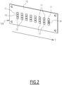
- the upper outer layer 10 comprises at least a first dielectric sublayer 12, for example made from ROGERS RO4350B material, and a plurality of first radiating elements 14 suitable for being fed with and radiating the signals to be transmitted.
- the first radiating elements 14 are made of electrically conductive material, for example copper, and are arranged spaced apart from each other on the first dielectric sublayer 12 substantially aligned in sequence along a reference horizontal axis Y that is perpendicular to the axis X.
- the first radiating elements 14 are preferably substantially identical to each other and each have a radiating area or surface "A1" measured in a plane transverse to the axis X, that is to say in the plane of the layer itself. For simplicity of illustration, this radiating area is clearly indicated in Figure 2 with oblique lines only for one radiating element 14.
- the first radiating elements 14 are of the type more precisely referred to as "patches", according to the nationally and internationally used term, with each having a substantially regular geometrical configuration, for example square or rectangular or circular.
- the upper outer layer 10 has a second sublayer 18, also referred to hereinafter as the first bonding sublayer 18, for example made from ROGERS RO4450 material, which is capable of enabling bonding of the upper outer layer 10 in its entirety with the layer of the plurality of layers immediately there-below.
- This first bonding sublayer 18 has a first thickness S1.
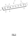
- the multilayer structure of the antenna 1 usefully comprises another inner layer 15, illustrated in Figure 3 , which is bonded to the first bonding sublayer 18, and is therefore interposed between the upper outer layer 10 and the first inner layer 20.
- the first inner layer 20 may be arranged immediately below and directly bonded in its upper part to the first bonding sublayer 18; in this case the further layer 15 is not used.
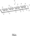
- the first inner layer 20 comprises at least an own first sublayer of conductive material 22, constituted for example of a copper foil, which is arranged on an own second sublayer of dielectric material 26.
- This second sublayer of dielectric material 26 may be prepared in a manner such as to have adhesive properties and enable bonding with the layer of the plurality of layers immediately there-below, that is to say in the illustrated exemplary embodiment with the second inner layer 30, or it may be combined with some adhesive material added so as to enable it to adhere to the subsequent layer.
- the first inner layer 20 comprises a plurality of through slots 24, having for example a U or C shaped form, which pass through the first sublayer of conductive material 22 and the second sublayer of dielectric material 26 and are suitable for conveying, towards at least the plurality of first radiating elements 14, the feeding signals to be radiated originating from the lower layers of the antenna 1 which will be described below.
- each through slot 24 is provided on the first inner layer 20 in an underlying position corresponding to the position of the associated first radiating element 14 on the upper outer layer 10.
- each slot 24 extends over the upper horizontal surface of the first inner layer 20 in a manner such that at least one end portion thereof is outside a virtual area obtained by projecting vertically (along the direction of the axis X) onto the first inner layer 20 itself the radiating surface "A1" of the associated first radiating element 14 or alternatively by projecting, again vertically, each slot 24 onto the first inner layer 20.
- each first radiating element 14 there is provided an associated pair of through slots 24, the two through slots 24 of each pair being formed on the first inner layer 20 in an underlying position corresponding to the position on the upper outer layer 10 of the associated first radiating element 14.
- the two slots of each pair of through slots 24, having for example a C or U shaped form, are arranged substantially perpendicular to each other.
- each slot 24 extends over the upper horizontal surface of the first inner layer 20 in a manner such that at least one end portion thereof extends outside a virtual area obtained by projecting vertically onto the first inner layer 20 itself the radiating surface "A1" of the associated first radiating element 14 (or alternatively by projecting, again vertically, each slot 24 onto the first inner layer 20).
- a plurality of metallised holes 29 passing through the sublayers 22 and 26 is defined.
- the second inner layer 30, which is attached above the sublayer 26, comprises at least an own first dielectric sublayer 32 (also referred to as third dielectric sublayer 32 to better distinguish it from the dielectric layers described previously) on which there is arranged a plurality of conductive lines 34, constituted for example of copper strips, that are suitable for conducting the feeding signals to be radiated at least towards the plurality of first radiating elements 14.
- an own first dielectric sublayer 32 also referred to as third dielectric sublayer 32 to better distinguish it from the dielectric layers described previously
- conductive lines 34 constituted for example of copper strips
- At least one corresponding conductive line 34 is associated with each radiating element.
- the third dielectric sublayer 32 acts as a bonding layer and therefore has adhesive properties or includes adhesive material in order to enable bonding with the layer of the plurality of layers immediately below the inner layer 30, that is to say in the exemplary embodiment illustrated with the further layer 40.
- the third dielectric sublayer 32 which may be made of or comprise for example ROGER RO4450 material, has an overall thickness S2 equal to or greater than the thickness S1 of the first bonding layer 18; in this manner, an improvement in the adapting or "matching" of the signals is advantageously obtained.
- the plurality of conductive lines 34 comprises for each first radiating element 14 a corresponding pair of conductive lines 34 associated therewith, and having for example shapes that differ from each other.
- each pair of conductive lines 34 comprises a first conductive line 34a, formed for example by a copper strip having a substantially rectilinear development, that is capable of transmitting to the corresponding first radiating element 14 the feeding signals to be radiated in a first direction of polarisation, and a second conductive line 34b, for example formed by an L-shaped copper strip, that is capable of transmitting to said corresponding first radiating element 14, the feeding signals to be radiated in a second direction of polarisation which is different from the first direction.
- These directions may coincide for example with the direction along the reference axis Z and the direction along the reference axis Y, illustrated in Figure 5 .
- the third inner layer 30 comprises metallised holes 29 that pass through its sublayers 34 and 32 and are vertically aligned each with a corresponding metallised through hole 29 formed on the first inner layer 20.
- each conductive line 34 extends over the plane of the sublayer 32 with the metallised holes 29 being arranged along both the edges of an associated conductive line 34 and replicating the path of the line itself.
- the conductive lines 34a and 34b of adjacent pairs of lines 34 are arranged in a mutually inverted sequence relative to each other. Furthermore, each line may be flipped to mirror-image or by 180° in the plane of the layer 30 itself, relative to the analogous preceding line.
- the inner layer 30 there is arranged: firstly, the first strip 34a that is capable of transmitting to the associated first radiating element 14 the feeding signals to be radiated in the first direction of polarisation; and then successively, the second conductive line 34b that is capable of transmitting to the same first radiating element 14 the feeding signals to be radiated in the second direction of polarisation.
- the second conductive strip 34b that is capable of transmitting to this subsequent radiating element 14 the feeding signals to be radiated in the second direction of polarisation, which is arranged with the L-shaped form flipped by 180° in the plane of the layer 30 relative to the analogous second line 34b of the preceding pair of lines; then, there is arranged the first line 34a (again flipped to mirror-image or by 180° relative to the analogous first line 34a of the preceding pair) that is capable of transmitting to the same subsequent radiating element 14 the feeding signals to be radiated in the first direction of polarisation.
- the inversion of the positioning order between the first strip 34a and the second strip 34b, with any relevant flipping relative to the analogous lines of the preceding pair, is regularly repeated at each subsequent radiating element 14 relative to the preceding one.
- the further layer 40 which is arranged below and is adjacent to the second inner layer 30, comprises at least an own first sublayer of conductive material 42 (hereinafter also referred to as second conductive sublayer 42 so as to distinguish it from the preceding sublayer 22), constituted for example of a copper foil, which is arranged on an own second dielectric sublayer 46 (hereinafter also referred to as fourth dielectric sublayer 46 so as to distinguish it from the previously described dielectric layers).
- second conductive sublayer 42 so as to distinguish it from the preceding sublayer 22
- fourth dielectric sublayer 46 so as to distinguish it from the previously described dielectric layers
- the fourth dielectric sublayer 46 as well may be made directly from a material having adhesive properties or be combined with added adhesive material.
- the further layer 40 has defined thereon a plurality of first through openings 44 passing through its sublayers 42 and 46.
- each of said first through openings 44 is formed on the layer 40, and in particular on the sublayer of conductive material 42, in a position corresponding to the position of at least one associated through slot 24 of the plurality of through slots 24 defined on the first sublayer of conductive material 22 of the first inner layer 20.
- each first through opening 44 delimits an area of through-passage "B", measured transversely relative to the reference axis X, which is substantially equal to at least ⁇ 2 /4, that is to say at least a quarter of the square of the wavelength ⁇ measured in the dielectric material formed by the entire assembly of the third dielectric sublayer 32 immediately above the sublayer of conductive material 42 and the fourth dielectric sublayer 46 immediately below the sublayer of conductive material 42.
- the further layer 40 comprises metallised holes 29 which pass through at least its sublayer 42 and are arranged on parallel rows that are each aligned with a corresponding metallised through hole 29 formed on the first inner layer 20 and on the second inner layer 30.
- the multilayer structure of the antenna 1 according to the invention usefully includes at least one further inner layer, denoted in Figures 1 and 2 by the reference numeral 15 which is interposed between the upper outer layer 10 and the first inner layer 20, and is in particular bonded to the first bonding layer 18 there-above.
- the inner layer 15 comprises at least an own dielectric sublayer 17, hereinafter also referred to as a further dielectric sublayer 17, which is also made for example from ROGERS RO4350B material, and a plurality of second radiating elements 16 arranged spaced apart from each other and suitable for being fed with and radiating the signals to be transmitted.
- a further dielectric sublayer 17 which is also made for example from ROGERS RO4350B material
- second radiating elements 16 arranged spaced apart from each other and suitable for being fed with and radiating the signals to be transmitted.
- the inner layer 15 also comprises a further bonding sublayer 19, for example made from ROGERS RO4450 material, which is capable of enabling the bonding of the inner layer 15 to the underlying first inner layer 20.
- a further bonding sublayer 19 for example made from ROGERS RO4450 material, which is capable of enabling the bonding of the inner layer 15 to the underlying first inner layer 20.
- the second radiating elements 16 are made of electrically conductive material, for example copper, and are arranged spaced apart from each other on the further dielectric sublayer 17, substantially aligned along the reference axis Y.
- each second radiating element 16 is placed below and substantially aligned, at a certain distance, with a corresponding first radiating element 14.
- each second radiating element 16 there is at least one conductive line 34, in particular at least the same conductive line 34 that is associated with the corresponding first radiating element 14 positioned there-above.
- each radiating element 16 is associated with a pair of conductive lines 34a and 34b; as a consequence thereof, each pair of conductive lines 34 is associated both with a corresponding second radiating element 16 as well as with the first radiating element 14 arranged above said corresponding second radiating element 16.
- the second radiating elements 16 are preferably substantially identical to each other and each extend over a radiating area or surface "A2" (for simplicity of illustration clearly indicated in Figure 1 with oblique lines only for one radiating element 16) and in the illustrated embodiment they are also of the so-called "patch" type.
- each second radiating element 16 has a geometric configuration that is substantially regular, for example square, rectangular or circular.
- the second radiating elements 16 have each a respective radiation area A2, the latter also measured on a plane transverse to the axis X, that is at most equal to or preferably less than the radiation area A1 of each of the first radiating elements 14.
- the presence of the further layer 15 provided with the second radiating elements 16 makes it possible to appropriately widen the range of operating frequencies of the antenna 1 according to the invention.
- each slot 24 extends over the upper horizontal surface of the first inner layer 20 in a manner such that at least one end portion thereof is outside a virtual area obtained by projecting vertically onto the further inner layer 15 itself the radiating surface "A2" of the associated second radiating element 16 (or alternatively by projecting, again vertically, each slot 24 onto the further inner layer 15).
- each slot 24 is represented only in Figure 3 in broken line obtained by virtually projecting the slots 24 onto the layer 15.
- an analogous configuration occurs in respect of at least one end portion of the slots 24 spilling out of the radiation areas A1 of the first radiating elements 14, even if this illustration has not been replicated in Figure 2 for simplicity.
- the multilayer structure of the antenna 1 may include one or more further layers.
- first additional layer 60 hereinafter indicated as the third inner layer 60
- second additional layer 70 hereinafter indicated as the fourth inner layer 70
- third additional layer 80 hereinafter indicated as the lower outer layer 80
- the antenna 1 in the antenna 1 according to the invention, it is possible to use only one of such additional layers, only two, e.g. the first and second additional layers 60 and 70, or the first and third additional layers 60 and 80, or the second and third additional layers 70 and 80, or all of them as it will be described in the following according to the exemplary configuration depicted in figure 1 .
- the first additional or third inner layer 60 is arranged below and is adjacent to the further inner layer 40, for example bonded to the fourth dielectric sublayer 46.
- the third inner layer 60 comprises an own first sublayer of conductive material 62 (hereinafter also referred to as third conductive sublayer 62 so as to distinguish it from the preceding conductive sublayers 22 and 42) which is made for example from a copper foil in order to bring the feed voltages to the control chips of the antenna 1 and is arranged on an own second dielectric sublayer 66 (hereinafter also referred to as fifth dielectric sublayer 66 so as to distinguish it from the previously described dielectric layers) made from a material having adhesive properties or combined with some added adhesive material.
- an own first sublayer of conductive material 62 hereinafter also referred to as third conductive sublayer 62 so as to distinguish it from the preceding conductive sublayers 22 and 42
- an own second dielectric sublayer 66 hereinafter also referred to as fifth dielectric sublayer 66 so as to distinguish it from the previously described dielectric layers
- second through openings 64 which pass through the third conductive sublayer 62 and the fifth dielectric sublayer 66; these second through openings 64, in terms of number and shape thereof, are preferably substantially identical to the first through openings 44, with each of them being substantially aligned with a corresponding first through opening 44 relative to a substantially vertical reference direction defined by the axis X.
- a plurality of metallised through holes are also defined on the third inner layer and in particular only on the third conductive sublayer 62 , analogous to the through holes 29 indicated above, which are also arranged so as to be aligned each with a corresponding metallised through hole 29 formed on the first inner layer 20 and on the further inner layer 40.
- the through holes also pass through the dielectric layer 46 and, seen along the vertical direction defined by the reference axis X, when the structure of the antenna 1 is assembled, form a plurality of through channels that start from the first sublayer of conductive material 22 and terminate in the third sublayer of conductive material 62, as schematically illustrated in dashed line in Figure 1 .
- these channels formed by the vertically aligned through holes 29 may terminate at the second sublayer of conductive material 42.
- this first additional layer 60 it will constitute the lower outer layer of the antenna 1, i.e. the layer located at the lowest position of the stack of layers used.
- the fourth inner sublayer 70 is arranged below and is adjacent to the third inner layer 60, for example bonded to the fifth dielectric sublayer 66.
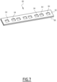
- the fourth inner layer 70 comprises at least an own first sublayer of conducting material 72 (hereinafter also referred to as fourth conducting sublayer 72 so as to distinguish it from the preceding conducting sublayers 22, 42 and 62), which is made for example from a copper foil that acts as a ground plane, and is arranged on an own second dielectric sublayer 76 (hereinafter also referred to as sixth dielectric sublayer 76 so as to distinguish it from the preceding dielectric sublayers) having adhesive properties.
- fourth conducting sublayer 72 so as to distinguish it from the preceding conducting sublayers 22, 42 and 62
- sixth dielectric sublayer 76 so as to distinguish it from the preceding dielectric sublayers
- these third through openings 74 are preferably substantially identical to the first through openings 44, with each of them being substantially aligned with a corresponding first through opening 44 relative to a substantially vertical reference direction defined by the axis X.
- first through openings 44, the second through openings 64, and the third through openings 74 are substantially aligned with each other along the vertical development of the multilayer structure.
- the third additional layer 80 will be arranged below and adjacent to the further inner layer 40, and if the second additional layer 70 is not used, the third additional layer will be arranged below and adjacent to the first additional layer 60.
- the third additional layer 80 is preferably meant to constitute the lower outer layer of the antenna 1.
- the antenna 1 further comprises at least one first series of parasitic radiating elements 11 and a second series of parasitic radiating elements 13 arranged on at least the said upper outer layer 10, in particular arranged on the first dielectric sublayer 14.
- the parasitic radiating elements 11 and 13 are arranged so as to be aligned along two rows that are parallel to each other with the plurality of first radiating elements 14 interposed between them.
- the series of parasitic radiating elements 11 and 13 serve to ameliorate the conformation of the irradiation beams of the transmitted signals.
- two further series of parasitic radiating elements may also be associated with the second radiating elements 16, where used; in this case, in a manner analogous to that which has been described above, these further parasitic radiating elements may be arranged on the sublayer of conductive material 17 along two parallel rows with the row of second radiating elements 16 interposed between them.
- the first control unit 210 of the system 200 is configured in a manner so as to select, in real time, at least one millimeter antenna 1 from among the four antennas 1 to which it is connected, from which the signals picked up at the input to the vehicle 100 are to be received, or to which signals to be radiated externally outside the vehicle 100 are to be transmitted, on the basis of one or more parameters indicative of the quality of the signal picked up at the input or transmitted at the output by each of the four millimeter antennas 1.
- the first control unit 210 is configured so as to select one single antenna 1 at a time, or to combine the signal received from multiple antennas 1 by means of digital or analogue methodologies, such as for example applying techniques including antenna array or diversity or MIMO ("Multiple Input - Multiple Output), of various types (amplitude and/or phase mixing of multiple signals performed in analogue or digital mode via Digital Signal Processing or DSP).
- digital or analogue methodologies such as for example applying techniques including antenna array or diversity or MIMO ("Multiple Input - Multiple Output), of various types (amplitude and/or phase mixing of multiple signals performed in analogue or digital mode via Digital Signal Processing or DSP).
- the selection of an antenna 1 is done by detecting the signal level (Received Signal Strength Indicator - RSSI) of each antenna 1 and choosing the antenna which provides the highest signal level (with the highest power).
- the first control unit 210 comprises a signal processor 212, such as for example a modem, connected to a control interface 214 for connecting the first control unit 210 to the various connection cables 211.
- a signal processor 212 such as for example a modem
- the control interface 4 of each antenna 1 comprises for example a frequency converter 4A and a control device 4B.
- the frequency converter 4A which is connected to the RF front-end module 3 and to the control device 4B, converts an input data signal at millimeter frequencies received by at least one of the radiating elements 14, 16 into a data signal at a first intermediate frequency for example between 1 GHz and 6 GHz (depending on the signal bandwidth) and converts an output data signal, originating from the signal processor 212 at the first intermediate frequency or at another frequency belonging to the same band of frequencies, into a data signal at millimeter frequencies in order to be transmitted by at least one radiating element 14, 16.
- control interface 214 of the first control unit 210 comprises a control device 216 which communicates with the control device 4B of each antenna 1, in order to conduct the control signals over the same coaxial cable 211 over which are transmitted the input and output data signals converted to the first intermediate frequency.
- control device 216 comprises for example an UP (type) frequency converter that is capable of converting the control signals to a second intermediate frequency that is different from the first intermediate frequency, for example comprised in the interval 0.1GHz and 1GHz.
- UP type
- the control device 216 comprises for example an UP (type) frequency converter that is capable of converting the control signals to a second intermediate frequency that is different from the first intermediate frequency, for example comprised in the interval 0.1GHz and 1GHz.
- the control device 216 of the control unit 210 further comprises one or more transceivers 226 for converting the control signals originating from the signal processor 212 into the second intermediate frequency.
- the control device 4B of the antenna 1 comprises for example a DOWN frequency converter that is capable of converting the control signals from the second intermediate frequency to a lower frequency in order to be able to control the frequency converter 4A and the RF front-end module 3.
- the control device 4B of each antenna 1 interprets the control signals and consequently acts on the associated frequency converter 4A and RF front-end module 3; to this end, the control device 4B comprises for example a transceiver (not shown in detail in the Figures) that converts the signals from the second intermediate frequency and a logic device, such as a microcontroller or an Application Specific Integrated Circuit (ASIC) or a Field Programmable Gate Array (FPGA) (also not shown in detail in the Figures).
- ASIC Application Specific Integrated Circuit
- FPGA Field Programmable Gate Array
- control unit 210 and each antenna 1 comprise respective power supply blocks (not illustrated in detail in the Figures) that communicate with each other through the respective coaxial connection cable 211.
- the control interface 214 comprises a plurality of DA/AD converter units 217, in which each DA/AD converter unit 217 is connected to a respective antenna 1 and comprises for example at least one analogue to digital converter (AD) and one digital to analogue converter (DA).
- AD analogue to digital converter
- DA digital to analogue converter
- the millimeter-wave data signal picked up at the input by at least one radiating element 14, 16 of an antenna 1 is amplified and routed over a correct path by the corresponding RF front-end module 3 towards the signal processor 212.
- the millimeter-wave data signal picked up at the input is sent to the frequency converter 4B which converts it to the first intermediate frequency in order to feed it onto the associated coaxial cable 211.
- This cable 211 transports it to one of the A/D converters of the converter unit 217 which digitizes the signal received and sends it to the signal processor 212.
- the signal processor 212 emits the output data signal in a digital format, and at least one DA converter of the unit of converters 217 converts it from digital to analogue at a first intermediate frequency.
- the output data signal at the first intermediate frequency is transmitted over at least one coaxial cable 211 and arrives at a frequency converter 4A of at least one antenna 1 which converts it to millimeter frequencies.
- the output data signal at millimeter frequency is amplified and routed by the respective front-end 3 to at least one radiating element 14, 16 which transmits it into the air.
- the control signals are generated by the signal processor 212 and are sent to the control device 216 which converts them to a second intermediate frequency and feeds them into one or more of the coaxial cables 211.
- the control signals at the second intermediate frequency then arrive at least at one control device 4B of an antenna 1 and are converted to a lower frequency suitable for controlling the associated frequency converter 4A and RF front-end module 3.
- the control interface 4 of each antenna 1 additionally also includes a DA/AD converter unit 4C comprising a digital/analogue (DA) converter and an analogue/digital (AD) converter designed to render the analogue signals suitable for digital transmission and vice versa.
- DA digital/analogue
- AD analogue/digital
- control device of each antenna 1 is for example capable of inserting into the flow of the input data signal also a signal for diagnosing its status.
- the control device 214 of the control unit 210 is capable of inserting into the flow of the output data signal also the control signals that serve to drive for each antenna the frequency converter 4A, the RF front-end module 3, and the DA/AD converter unit.
- the control device 4B of each antenna is capable of separating the output data signal from the control signals.
- the control device 214 of the unit 210 is capable of separating the input data signal from the diagnostics signal.
- control device 4B of each antenna 1 comprises digital transmission controllers, serialisers/deserialisers that are capable of encapsulating/decapsulating and digital signals and a computing unit (for example a microcontroller, ASIC or FPGA) for the management of the devices of the antennas 1, and the control device 214 of the control unit 210 comprises for example digital transmission controllers and serialisers/deserialisers that are capable of encapsulating/decapsulating digital signals.
- some poles of the digital cable 211 may be dedicated to the transport of DC power supply, thereby avoiding the need for ad hoc power supply blocks.
- an input data signal at millimeter frequency is picked up by at least one radiating element 14, 16 of an antenna 1 and sent to the corresponding RF front-end module 3 which amplifies and routes it.
- the input data signal is converted by the frequency converter 4A from the millimeter frequency to an intermediate frequency between for example 0.1 GHz and 6 GHz. Then the input data signal is digitised by an AD converter of the converter unit 4C.
- the control device 4B encapsulates the input data signal together with the diagnostics signal in a digital communication protocol, in a manner so as to obtain an encapsulated signal, and transmits it in digital format over the corresponding digital cable 211.
- the signal encapsulated in digital format then arrives at the control device 216 of the control unit 210 which decapsulates it in a manner so as to obtain the input data signal which is sent to the signal processor 212.
- the signal processor 212 emits the output data signal in a digital format.
- the control device 216 encapsulates the output data signal with the control signals in a manner so as to obtain an encapsulated signal which is transmitted over the digital cables 211.
- the encapsulated signal is received by the control device 4B of at least one antenna 1 and is decapsulated, in a manner so as to obtain the output data signal in digital format.
- the output data signal in digital format is sent to a DA converter of the converter unit 4C which converts it into analogue.
- the analogue output data signal is converted to a millimeter frequency by the frequency converter 4A.
- the output data signal at millimeter frequencies is amplified and routed by the corresponding RF front-end module 3 towards at least one of the radiating elements 14, 16 of the antenna 1 which transmits it into the air.
- the control signals are generated by the signal processor 212 in digital format and are sent to the control device 216 of the central control unit which encapsulates them together with the output data signal so as to obtain the encapsulated signal which is transmitted over one or more digital cables 211.
- the encapsulated signal (comprising the output data signal and the control signals) is received by the control device 4B of at least one antenna 1 which decapsulates the signal so as to obtain the digital control signals for controlling respectively the respective frequency converter 4A, the RF front-end module 3 and the DA/AD converter unit 4C.
- the antennas 1 can receive/transmit signals by means of their respective digital cables 211 that are connected to respective dedicated data buses, or it is possible to use a single shared data bus.
- the various signals that travel in the shared data bus have one address (shared band) and the identification of the correct sender/receiver takes place by means of the transmission protocol headers inserted by the respective control devices that encapsulate the signals to be sent over the shared data bus.
- the data transceiver system 200 installed on board the vehicle 100 additionally comprises also a second set of antennas 230 for transceiving of data in a frequency band lower than the operating band of the first set of millimeter-wave antennas 1.
- the data transceiver system 200 preferably comprises a second control unit 250 which is operatively associated with and is configured to control the operation of the second set of antennas 230.
- the data transceiver system 200 further comprises at least one further antenna 240 for transceiving of data in an intermediate frequency band between the operating frequency bands of said first and second sets of antennas 1, 230, and the second control unit 250 is also operatively associated with and is configured to control the operation of the at least one further antenna 240.
- the second control unit 250 is connected to the antennas 230 and/or 240, for example by means of respective cables 231.
- the second set of antennas 230 also comprises at least four antennas 230 which are each installed in a corresponding quadrant of said four quadrants A, B, C, D, and of which, a first and a second antennas 230 are installed at the front bumper 106 of the vehicle, for example in proximity to the respective headlights 101 and 102, and a third and a fourth antennas 230 are installed at the rear bumper 107, for example in proximity to the respective taillights 103 and 104.
- the four antennas 230 operate at a frequency lower than or equal to 5GHz.
- said at least one further antenna 240 may be installed on the roof 108 of the vehicle 100, for example within a cupole or shark fin antenna or it may also be installed internally inside the vehicle, for example in proximity to the internal rear-view mirror, or it is possible to use two antennas 240 contemporaneously.
- the or each antenna 240 operates at a frequency in the region of 5.9 GHz, and is dedicated to the transceiving of Vehicle-to-Everything (V2X) data.
- V2X Vehicle-to-Everything
- the antennas 230 and the or each further antenna 240 may be of a type that is commercially available in the market and for this reason they are not described in detail herein.
- the vehicle 100 according to the invention allows achieving the intended object since the data transceiver system 200 installed on board represents a good compromise between the number of antennas installed, in particular of the millimeter-wave type, and effectiveness of the data transmission/reception coverage around the vehicle 100, with optimized occupation of space and encumbrances. Furthermore, the structure of the antenna 1 described previously makes it possible to obtain a solution that combines transmission/reception efficiency with reduced overall dimensions and production costs. Clearly, where possible or required, it is possible to add to the optimized configuration described above, one or more further antennas.
- the four millimeter-wave antennas 1 were all installed to be coincident with the respective four head/taillights or head/taillight assemblies, it is possible to add one or more antennas 1 installed in the corresponding side bumpers 109, or vice versa, if the four antennas 1 were installed in the respective side bumpers 109, it is possible to add one or more antenna(s) 1 installed in the corresponding head/taillights or head/taillight assemblies.
Landscapes
- Engineering & Computer Science (AREA)
- Remote Sensing (AREA)
- Physics & Mathematics (AREA)
- Electromagnetism (AREA)
- Variable-Direction Aerials And Aerial Arrays (AREA)
- Circuits Of Receivers In General (AREA)
- Measuring Pulse, Heart Rate, Blood Pressure Or Blood Flow (AREA)
Description
- The present invention relates to a vehicle, in particular a road vehicle, comprising a system that is optimized for transceiving data and configured in particular to operate in the 5G frequency band.
- In the description that follows, by way of a possible example of a vehicle, reference will be made to an automobile without thereby intending in any way to limit the realization of the present invention in the form of other types of road vehicles, such as for example buses, trucks, commercial vehicles, etc.
- As is known, the use of so-called "infotainment" systems on board vehicles, such as automobiles (or cars), is widespread. In fact, vehicles currently on the road integrate many services ranging from entertainment, for example audio and/or television, to telephony, to driving assistance, with a view to ensuring ever greater travel safety and comfort for users.
- Consequently, the data traffic that vehicles happen to be transceiving has assumed ever increasing proportions, thus requiring the implementation of ever faster and more reliable communication systems.
- In this regard, vehicles are also impacted by the on board use of the most recent so-called 5G communication system, to which millimeter-wave (mmW) frequency bands have been allocated.
- Clearly, for the appropriate functioning of the communications one of the fundamental components for the proper transceiving of data is represented by antennas which are usually subject to problems related to the attenuation of signals due to propagation in free spaces or the presence of obstacles.
- Such problems are particularly accentuated in the millimeter-wave frequency bands and even more so in the case of vehicles where the structure of the vehicle itself and the materials used, such as the metal bodywork, happen to be shielding. In these conditions, depending on the installation of the antenna on a vehicle and its position during travel, the quality of the data communication with the base radio stations external to the vehicle may prove to be unsatisfactory or it may in any case be necessary to adopt on board the vehicle antenna configurations that are as redundant as possible. In the latter case, however, the overall cost of the communication systems increases, in addition to there being installation problems, in particular on board automobiles where the space available for the antennas is limited.
-
US 2020/185819 A1 discloses an antenna system which is installed on a vehicle and comprises a first antenna system having a plurality of first antenna elements disposed within a structure mounted in the vehicle, to perform Multi Input Multi Output (MIMO), and a second antenna system having a plurality of second antenna elements attached to side surfaces of a polyhedron disposed within the structure, to perform beamforming. -
US 2018/288672 A1 discloses a vehicle-mounted millimeter-wave communication device which includes an acquisition unit for acquiring a relay request that requests relay of communication from a first communication partner, a detection unit for detecting directions of the first communication partner and a second communication partner that are viewed from the vehicle, and a communication control unit for performing control such that, in the case where the relay request is received from the first communication partner and it is possible to communicate with the second communication partner, communication, in which a communication time longer than a communication time set for another direction is set for each of the directions of the first communication partner and the second communication partner, is performed, and communication between the first communication partner and the second communication partner is relayed. -
EP 1612954 A2 discloses a vehicle which has a transmitting/receiving component for transmitting information, operation data and/or commands to a nearby vehicle or to nearby compartment of same vehicle, wherein the component operates at range of 20-70 Giga hertz. The component that is designed as a high frequency radio antenna is integrated into a lens and/or clear-view screen of a frontal illumination device and/or signal device. -
DE 102013021819 A1 discloses a radar device for a motor vehicle, with a vehicle light for illuminating the motor vehicle surroundings, and with a radar sensor for detecting target objects located in the surroundings. The radar sensor has an antenna unit that is arranged in a housing interior of the vehicle light, for emitting/receiving electromagnetic radar waves. A controller activates the antenna unit and is arranged outside the housing interior of the vehicle light. The radar sensor has a connecting unit via which the controller is electrically coupled to the antenna unit through a housing wall of the housing. -
WO 2021/133408 A1 , representing a prior right under Article 54(3) EPC, discloses a vehicle having antennas elements which include antennas arrays that can support various communication technologies and can be integrated into different components or subcomponents of the vehicle. - The main object of the present invention is to mitigate these problems, and in particular to offer a solution that makes it possible to find an appropriate balance between the requirement to adequately cover the signal transceiver field around the vehicle and the need for an optimized number of antennas.
- This main object, as well as any other objects which will emerge more clearly from the description that follows, are achieved by a vehicle, in particular a road vehicle, such as an automobile, as defined in claim 1.
- Particular embodiments constitute the subject matter of the dependent claims, the content of which is to be understood as an integral part of the present description.
- Further characteristics and advantages of the invention will become apparent from the detailed description that follows, set forth purely by way of non-limiting example, with reference to the attached drawings, in which:
-
Figure 1 schematically illustrates one possible stratigraphic embodiment of a millimeter-wave antenna installed on board the vehicle according to the present invention; -
Figures 2 to 8 schematically illustrate portions of some layers that are usable in the antenna shown inFigure 1 ; -
Figure 9 schematically illustrates a block diagram of a data transceiver system installed on board the vehicle according to the invention; -
Figure 10 is a top view that schematically illustrates a vehicle according to the invention; -
Figure 11 is a detail that schematically illustrates a millimeter-wave antenna installed in a headlight assembly of a vehicle according to the invention. - It should be noted that in the detailed description that follows, components that are identical or similar, from a structural and/or functional standpoint, may have the same or different reference numerals, regardless of whether they are shown in different embodiments of the present invention or in distinct parts.
- It should also be noted that, in order to clearly and concisely describe the present invention, the drawings may not necessarily be to scale and some characteristic features of the description may be shown in a somewhat schematic form.
- Furthermore, where the terms "adapted", or "organised ", or "configured", or "shaped", or " set ", or any similar term may eventually be used in the present document, with reference being made to any component in its entirety, or to any part of a component or a combination of components, it is to be understood that it refers to and correspondingly includes the structure and/or configuration and/or form and shape and/or positioning.
- In particular, when these terms refer to electronic hardware or software means, they are to be understood as including circuits or parts of electronic circuits, as well as software/firmware, such as for example algorithms, routines and programs in general, that may be running and/or residing in any storage medium.
- In addition, where the term "substantial" or "substantially" is used herein, it is to be understood as including an actual variation of plus or
minus 5% relative to what indicated as the reference value, axis or position; and where the terms "transverse" or "transversely" are used herein, they are to be understood as including a direction that is not parallel to the reference part or parts or direction(s)/axes to which they refer, and perpendicularity is to be considered as a specific case of transverse direction. - Finally, in the description and in the claims that follow, the ordinal numerals first, second, et cetera, will be used for purposes of illustrative clarity and in no way should they be construed as limiting for any reason whatsoever; in particular, the indication for example, of a "first layer", or of a first "first sublayer...", does not necessarily imply the presence or the stringent requirement, in all the embodiments, of a further "second layer" or "second sublayer" or vice versa, unless this presence is clearly evident for the proper operation of the described embodiments, nor that the order is to be identical to the sequence described with reference to the illustrated exemplary embodiments.
-
Figure 10 schematically illustrates a vehicle according to the invention, indicated by thereference numeral 100, in which a system for transceiving data is installed on board the vehicle itself; an exemplary embodiment of this system for the transceiving of data is illustrated inFigure 9 and indicated therein by theoverall reference numeral 200. - Usefuly, the
system 200 installed on board thevehicle 100 comprises at least one first set of millimeter-wave antennas 1 for the transceiving of data in the 5G frequency band, in particular with frequencies equal to or greater than 20 Ghz and up to 100 GHz, and in which, with respect to an imaginary first plane E and an imaginary second plane F that are perpendicular to each other and that virtually divide thevehicle 100 into four quadrants A, B, C, D, the said at least one first set of millimeter-wave antennas 1 comprises at least four antennas 1, which are each installed in a corresponding quadrant of the said four quadrants A, B, C, D, and an embodiment of which is illustrated inFigures 1-8 . - Depending on the dimensions of the vehicle, these four quadrants A, B, C and D may be substantially identical to or different from each other, and the planes E and F are to be considered to be drawn, for example, in a manner such as to include the two corresponding direct centre-line axes one along the line joining front-rear of the vehicle, and the other along the line joining the lateral sides of the same.
- In any case, at least the two front quadrants A and B are to be considered identical to each other and the two rear quadrants C and D are also to be considered identical to each other.
- The millimeter antennas 1 may be substantially identical to each other or, depending on the requirements, it is possible to simultaneously use millimeter antennas that are different from each other in construction.
- In particular, and as will become apparent in more detail from the description that follows, at least one of the four millimeter-wave antennas 1 used, preferably each of them, comprises at least one
radiating element 14, and is arranged in the respective quadrant A, B, C, D in a manner so that between the at least oneradiating element 14 and the surface external to thevehicle 100 towards which irradiation is to occur or from which signals are to be received, there are interposed one or more surfaces of non-metallic material and having a coefficient of loss (also referred to as dissipation factor "tan δ" and equal to the ratio between the active power and reactive power absorbed by the material) lower than 0.1. - In one possible embodiment, at least one of said four millimeter-wave antennas 1 is arranged to be coincident with a left front headlight or
headlight assembly 101 or right front headlight orheadlight assembly 102, or with a left rear taillight ortaillight assembly 103 or right rear taillight ortaillight assembly 104. - In one possible embodiment, at least one of the said four millimeter-wave antennas 1 is arranged to be coincident with one of the front or
rear doors 112 of thevehicle 100. In this configuration, the at least one antenna 1 may be integrated into the structure of a side bumper 109 (emphasized inFigure 10 for greater clarity of illustration) applied externally to thecorresponding door 112, or may be arranged in the interspace defined between aside bumper 109 and the associateddoor 112. - In particular, according to one possible embodiment illustrated in
Figure 10 , among the four antennas 1: a first antenna 1 is arranged to be coincident with a leftfront headlight 101 or leftfront headlight assembly 101 of thevehicle 100; a second antenna 1 is arranged to be coincident with a rightfront headlight 102 or rightfront headlight assembly 102 of thevehicle 100; a third antenna 1 is arranged to be coincident with a leftrear taillight 103 or leftrear taillight assembly 103 of thevehicle 100; and a fourth antenna 1 is arranged to be coincident with a rightrear taillight 104 or rightrear taillight assembly 104 of thevehicle 100. - Alternatively, according to one possible embodiment represented in
Figure 10 with broken lines, among the four antennas 1, for avehicle 100 equipped with four side doors 111, a first antenna 1 is arranged to be coincident with aside bumper 109 mounted on theleft front door 112; a second antenna 1 is arranged to be coincident with aside bumper 109 mounted on the right front door; a third antenna 1 is arranged to be coincident with aside bumper 109 mounted on the leftrear door 112; and a fourth antenna 1 is arranged to be coincident with aside bumper 109 mounted on theleft front door 112. - Clearly, in the
vehicle 100 according to the invention it is possible to implement a combined configuration in which, among the four millimeter-wave antennas 1, one or more antennas 1 are mounted to be coincident with headlights or headlight assemblies, and one or more of the remaining antennas 1 are mounted to be coincident withside bumpers 109. - A preferred embodiment of at least one of the millimeter-wave antennas 1 is illustrated in
Figures 1-8 . - In particular, the antenna 1 comprises a containment casing, schematically illustrated in
Figure 1 by thereference numeral 2, which houses inside it all or at least part of the components of the antenna. Thiscontainment casing 2 is for example made of plastic material and is conveniently mounted integrated on the reflector of a corresponding front headlight or headlight assembly, or rear taillight or taillight assembly of thevehicle 100, for example as illustrated inFigure 11 for the rightfront headlight assembly 102. - In this possible embodiment, the antenna 1 may be substantially integrated into the structure of the associated head/taillight assembly, with its
own containment casing 2 which is inserted in a suitable housing formed in the body of the reflector of the associated head/taillight or head/taillight assembly vehicle 100, is substantially coplanar with the surface of the reflector itself. - Analogously, the antenna 1 can be substantially integrated into the structure of the associated
side bumper 109, with itsown containment casing 2 which is inserted in a suitable housing formed in the body of the bumper, for example in a manner such that its external surface, which faces the environment external to thevehicle 100, is substantially coplanar with the external surface of the side bumper itself. - In the
vehicle 100 according to the invention, the four antennas 1 are connected, for the purposes and functionalities that will be described in detail below, to afirst control unit 210 that is installed on the vehicle in a remote position distant from the antennas 1, and is connected to the antennas 1 by means ofcorresponding connection cables 211 which may be coaxial or digital type cables depending on the applications. - As illustrated in
Figure 1 andFigure 9 (in the latter Figure, for only one antenna 1 for simplicity of description) each antenna 1 comprises, arranged inside the casing 2: - a
multilayer structure 5; - an RF (Radio Frequency) front-
end module 3 which comprises a circuitry for managing the signal transmitted or received by theradiating element 14 and, where present, the beamsteering/beamforming functionalities, which may be implemented with the analogue, or digital, or hybrid digital/analogue method; and - a
control interface 4 for connecting the antenna 1 to acorresponding connection cable 211. - For simplicity of illustration, in the example schematically illustrated in
Figure 1 , the RF front-end module 3 has been represented as a separate module that is connected to themultilayer structure 5. Clearly, depending on the applications, the RF front-end module 3 could be connected to the multilayer structure in this configuration, or it could be integrated therewith, in the form of further additional layers and/or by using some of the layers of themultilayer structure 5 described below, such as for example one or more of thelayers - In more detailed terms, the
multilayer structure 5 comprises a plurality of layers stacked vertically along the reference direction indicated inFigure 1 by the reference axis X, the said multilayer structure including at least: - an upper outer layer 10;
- a first
inner layer 20 arranged below the upper outer layer 10; - a second
inner layer 30 arranged below and adjacent to the firstinner layer 20; and - a
further layer 40 arranged below and adjacent to the secondinner layer 30. - In particular, in the possible embodiment illustrated in
Figures 1 and2 , the upper outer layer 10 comprises at least a firstdielectric sublayer 12, for example made from ROGERS RO4350B material, and a plurality of firstradiating elements 14 suitable for being fed with and radiating the signals to be transmitted. - The first
radiating elements 14 are made of electrically conductive material, for example copper, and are arranged spaced apart from each other on the firstdielectric sublayer 12 substantially aligned in sequence along a reference horizontal axis Y that is perpendicular to the axis X. - The
first radiating elements 14 are preferably substantially identical to each other and each have a radiating area or surface "A1" measured in a plane transverse to the axis X, that is to say in the plane of the layer itself. For simplicity of illustration, this radiating area is clearly indicated inFigure 2 with oblique lines only for one radiatingelement 14. - In the illustrated exemplary embodiment, the
first radiating elements 14 are of the type more precisely referred to as "patches", according to the nationally and internationally used term, with each having a substantially regular geometrical configuration, for example square or rectangular or circular. - In the embodiment illustrated in
Figure 1 , the upper outer layer 10 has asecond sublayer 18, also referred to hereinafter as thefirst bonding sublayer 18, for example made from ROGERS RO4450 material, which is capable of enabling bonding of the upper outer layer 10 in its entirety with the layer of the plurality of layers immediately there-below. Thisfirst bonding sublayer 18 has a first thickness S1. - According to one possible embodiment illustrated in
Figure 1 , and for the purposes which will be described in more detail below, the multilayer structure of the antenna 1 usefully comprises anotherinner layer 15, illustrated inFigure 3 , which is bonded to thefirst bonding sublayer 18, and is therefore interposed between the upper outer layer 10 and the firstinner layer 20. - Alternatively, in one possible embodiment, the first
inner layer 20 may be arranged immediately below and directly bonded in its upper part to thefirst bonding sublayer 18; in this case thefurther layer 15 is not used. - As illustrated in
Figures 1 and4 , the firstinner layer 20 comprises at least an own first sublayer ofconductive material 22, constituted for example of a copper foil, which is arranged on an own second sublayer ofdielectric material 26. This second sublayer ofdielectric material 26 may be prepared in a manner such as to have adhesive properties and enable bonding with the layer of the plurality of layers immediately there-below, that is to say in the illustrated exemplary embodiment with the secondinner layer 30, or it may be combined with some adhesive material added so as to enable it to adhere to the subsequent layer. - Usefully, the first
inner layer 20 comprises a plurality of throughslots 24, having for example a U or C shaped form, which pass through the first sublayer ofconductive material 22 and the second sublayer ofdielectric material 26 and are suitable for conveying, towards at least the plurality offirst radiating elements 14, the feeding signals to be radiated originating from the lower layers of the antenna 1 which will be described below. - In particular, in the antenna 1 according to the invention for each
first radiating element 14 there is provided at least one correspondingslot 24 operatively associated thereto; with reference to the substantially vertical direction indicated inFigure 1 by the axis X, each throughslot 24 is provided on the firstinner layer 20 in an underlying position corresponding to the position of the associated first radiatingelement 14 on the upper outer layer 10. - Preferably, with reference to the vertical direction represented by the axis X, each
slot 24 extends over the upper horizontal surface of the firstinner layer 20 in a manner such that at least one end portion thereof is outside a virtual area obtained by projecting vertically (along the direction of the axis X) onto the firstinner layer 20 itself the radiating surface "A1" of the associated first radiatingelement 14 or alternatively by projecting, again vertically, eachslot 24 onto the firstinner layer 20. - In one possible embodiment, as illustrated in the example of
Figure 4 , for eachfirst radiating element 14 there is provided an associated pair of throughslots 24, the two throughslots 24 of each pair being formed on the firstinner layer 20 in an underlying position corresponding to the position on the upper outer layer 10 of the associated first radiatingelement 14. - In the illustrated exemplary embodiment, the two slots of each pair of through
slots 24, having for example a C or U shaped form, are arranged substantially perpendicular to each other. - Also in this case, with reference to the vertical direction represented by the axis X, each
slot 24 extends over the upper horizontal surface of the firstinner layer 20 in a manner such that at least one end portion thereof extends outside a virtual area obtained by projecting vertically onto the firstinner layer 20 itself the radiating surface "A1" of the associated first radiating element 14 (or alternatively by projecting, again vertically, eachslot 24 onto the first inner layer 20). - Furthermore, at least on the first inner layer 20 a plurality of
metallised holes 29 passing through thesublayers - As illustrated in
Figures 1 and5 , the secondinner layer 30, which is attached above thesublayer 26, comprises at least an own first dielectric sublayer 32 (also referred to asthird dielectric sublayer 32 to better distinguish it from the dielectric layers described previously) on which there is arranged a plurality ofconductive lines 34, constituted for example of copper strips, that are suitable for conducting the feeding signals to be radiated at least towards the plurality offirst radiating elements 14. - In particular, at least one corresponding
conductive line 34 is associated with each radiating element. - In one possible embodiment, the
third dielectric sublayer 32 acts as a bonding layer and therefore has adhesive properties or includes adhesive material in order to enable bonding with the layer of the plurality of layers immediately below theinner layer 30, that is to say in the exemplary embodiment illustrated with thefurther layer 40. - In particular, the
third dielectric sublayer 32, which may be made of or comprise for example ROGER RO4450 material, has an overall thickness S2 equal to or greater than the thickness S1 of thefirst bonding layer 18; in this manner, an improvement in the adapting or "matching" of the signals is advantageously obtained. - According to the embodiment illustrated in
Figure 5 , the plurality ofconductive lines 34 comprises for each first radiating element 14 a corresponding pair ofconductive lines 34 associated therewith, and having for example shapes that differ from each other. - More in detail, according to this embodiment, each pair of
conductive lines 34 comprises a firstconductive line 34a, formed for example by a copper strip having a substantially rectilinear development, that is capable of transmitting to the corresponding first radiatingelement 14 the feeding signals to be radiated in a first direction of polarisation, and a secondconductive line 34b, for example formed by an L-shaped copper strip, that is capable of transmitting to said corresponding first radiatingelement 14, the feeding signals to be radiated in a second direction of polarisation which is different from the first direction. These directions may coincide for example with the direction along the reference axis Z and the direction along the reference axis Y, illustrated inFigure 5 . - Furthermore, also the third
inner layer 30 comprises metallisedholes 29 that pass through its sublayers 34 and 32 and are vertically aligned each with a corresponding metallised throughhole 29 formed on the firstinner layer 20. - Conveniently, each
conductive line 34 extends over the plane of thesublayer 32 with the metallised holes 29 being arranged along both the edges of an associatedconductive line 34 and replicating the path of the line itself. - Furthermore, in one possible embodiment illustrated in
Figure 5 , theconductive lines lines 34 are arranged in a mutually inverted sequence relative to each other. Furthermore, each line may be flipped to mirror-image or by 180° in the plane of thelayer 30 itself, relative to the analogous preceding line. - More in detail, with reference to a direction of displacement along the axis Y, starting from the outer
transverse edge 31 in a position corresponding to the positioning on the upper outer layer 10 of thefirst radiating element 14 arranged closest to theleft edge 11, on theinner layer 30 there is arranged: firstly, thefirst strip 34a that is capable of transmitting to the associated first radiatingelement 14 the feeding signals to be radiated in the first direction of polarisation; and then successively, the secondconductive line 34b that is capable of transmitting to the samefirst radiating element 14 the feeding signals to be radiated in the second direction of polarisation. Continuing along the direction Y, coincident with the position of the subsequentfirst radiating element 14 on the upper outer layer 10, on thelayer 30, there is arranged the second pair ofconductive lines line conductive strip 34b, that is capable of transmitting to thissubsequent radiating element 14 the feeding signals to be radiated in the second direction of polarisation, which is arranged with the L-shaped form flipped by 180° in the plane of thelayer 30 relative to the analogoussecond line 34b of the preceding pair of lines; then, there is arranged thefirst line 34a (again flipped to mirror-image or by 180° relative to the analogousfirst line 34a of the preceding pair) that is capable of transmitting to the samesubsequent radiating element 14 the feeding signals to be radiated in the first direction of polarisation. The inversion of the positioning order between thefirst strip 34a and thesecond strip 34b, with any relevant flipping relative to the analogous lines of the preceding pair, is regularly repeated at eachsubsequent radiating element 14 relative to the preceding one. - Furthermore, in one possible embodiment, one or more of the
conductive lines 34, preferably all of them, comprise each at least one section of line derived in parallel along the correspondingconductive line 34, preferably arranged to be coincident with the transition zone which in the exemplary embodiment happens to be close to the outer edge of the layer, but which in general could be found within a wider layer, and in particular to be coincident with a transition of a radiofrequency signal, capable of shifting the signal itself onto a different layer of the antenna, without introducing significant losses. This derived section makes it possible to artificially introduce alterations that serve to further enhance the so-called "matching" of the signal transition zones. - This derived section of line may be constituted, for example, by a further portion of strip, and is illustrated in
Figure 5 by thereference numeral 34c only for one pair ofconductive lines 34 for the sake of simplicity of description. - As illustrated in more detail in
Figure 6 , thefurther layer 40, which is arranged below and is adjacent to the secondinner layer 30, comprises at least an own first sublayer of conductive material 42 (hereinafter also referred to as secondconductive sublayer 42 so as to distinguish it from the preceding sublayer 22), constituted for example of a copper foil, which is arranged on an own second dielectric sublayer 46 (hereinafter also referred to asfourth dielectric sublayer 46 so as to distinguish it from the previously described dielectric layers). - The
fourth dielectric sublayer 46 as well may be made directly from a material having adhesive properties or be combined with added adhesive material. - In particular, the
further layer 40 has defined thereon a plurality of first throughopenings 44 passing through its sublayers 42 and 46. - More in detail, with reference to the substantially vertical direction indicated in
Figure 1 by the axis X, each of said first throughopenings 44 is formed on thelayer 40, and in particular on the sublayer ofconductive material 42, in a position corresponding to the position of at least one associated throughslot 24 of the plurality of throughslots 24 defined on the first sublayer ofconductive material 22 of the firstinner layer 20. - Conveniently, in one possible embodiment, with reference to the operation of the antenna 1 at the nominal operating frequency, each first through
opening 44 delimits an area of through-passage "B", measured transversely relative to the reference axis X, which is substantially equal to at least λ2/4, that is to say at least a quarter of the square of the wavelength λ measured in the dielectric material formed by the entire assembly of thethird dielectric sublayer 32 immediately above the sublayer ofconductive material 42 and thefourth dielectric sublayer 46 immediately below the sublayer ofconductive material 42. - For the sake of simplicity in illustration, in
Figure 6 the area of through-passage "B" has been represented with oblique lines only for oneopening 44. - In this manner, the presence of through
openings 44 formed in particular on the sublayer ofconductive material 42, which acts as a ground plane, substantially prevents the presence of reflection effects which would affect the quality of the signals transmitted, while providing for optimized overall dimensions and low costs as compared to different solutions aimed at tackling the same problem. - Furthermore, in the illustrated exemplary embodiment, also the
further layer 40 comprises metallisedholes 29 which pass through at least itssublayer 42 and are arranged on parallel rows that are each aligned with a corresponding metallised throughhole 29 formed on the firstinner layer 20 and on the secondinner layer 30. - As previously mentioned, in one possible embodiment, the multilayer structure of the antenna 1 according to the invention usefully includes at least one further inner layer, denoted in
Figures 1 and2 by thereference numeral 15 which is interposed between the upper outer layer 10 and the firstinner layer 20, and is in particular bonded to thefirst bonding layer 18 there-above. - In the embodiment illustrated, the
inner layer 15 comprises at least anown dielectric sublayer 17, hereinafter also referred to as afurther dielectric sublayer 17, which is also made for example from ROGERS RO4350B material, and a plurality ofsecond radiating elements 16 arranged spaced apart from each other and suitable for being fed with and radiating the signals to be transmitted. - In the embodiment illustrated in
Figure 1 , theinner layer 15 also comprises afurther bonding sublayer 19, for example made from ROGERS RO4450 material, which is capable of enabling the bonding of theinner layer 15 to the underlying firstinner layer 20. - The
second radiating elements 16 are made of electrically conductive material, for example copper, and are arranged spaced apart from each other on thefurther dielectric sublayer 17, substantially aligned along the reference axis Y. - In particular, relative to the substantially vertical reference direction indicated by the axis X, each
second radiating element 16 is placed below and substantially aligned, at a certain distance, with a corresponding first radiatingelement 14. - In this case, associated with each
second radiating element 16 there is at least oneconductive line 34, in particular at least the sameconductive line 34 that is associated with the corresponding first radiatingelement 14 positioned there-above. - In the illustrated embodiment, each radiating
element 16 is associated with a pair ofconductive lines conductive lines 34 is associated both with a correspondingsecond radiating element 16 as well as with thefirst radiating element 14 arranged above said corresponding second radiatingelement 16. - The
second radiating elements 16 are preferably substantially identical to each other and each extend over a radiating area or surface "A2" (for simplicity of illustration clearly indicated inFigure 1 with oblique lines only for one radiating element 16) and in the illustrated embodiment they are also of the so-called "patch" type. - In the illustrated embodiment, each
second radiating element 16 has a geometric configuration that is substantially regular, for example square, rectangular or circular. - Conveniently, the
second radiating elements 16 have each a respective radiation area A2, the latter also measured on a plane transverse to the axis X, that is at most equal to or preferably less than the radiation area A1 of each of thefirst radiating elements 14. - In practice, the presence of the
further layer 15 provided with thesecond radiating elements 16 makes it possible to appropriately widen the range of operating frequencies of the antenna 1 according to the invention. - Preferably, with reference to the vertical direction represented by the axis X, also in this case each
slot 24 extends over the upper horizontal surface of the firstinner layer 20 in a manner such that at least one end portion thereof is outside a virtual area obtained by projecting vertically onto the furtherinner layer 15 itself the radiating surface "A2" of the associated second radiating element 16 (or alternatively by projecting, again vertically, eachslot 24 onto the further inner layer 15). - For illustrative purposes, this end portion of each
slot 24 is represented only inFigure 3 in broken line obtained by virtually projecting theslots 24 onto thelayer 15. As previously described, an analogous configuration occurs in respect of at least one end portion of theslots 24 spilling out of the radiation areas A1 of thefirst radiating elements 14, even if this illustration has not been replicated inFigure 2 for simplicity. - According to further possible embodiments, the multilayer structure of the antenna 1 may include one or more further layers.
- In particular, in the exemplary embodiment of
Figure 1 , there are for example illustrated a first additional layer 60 (hereinafter indicated as the third inner layer 60), a second additional layer 70 (hereinafter indicated as the fourth inner layer 70), and a third additional layer 80 (hereinafter indicated as the lower outer layer 80). - However, it has to be understood that, according to the applications, in the antenna 1 according to the invention, it is possible to use only one of such additional layers, only two, e.g. the first and second
additional layers additional layers additional layers figure 1 . - The first additional or third
inner layer 60 is arranged below and is adjacent to the furtherinner layer 40, for example bonded to thefourth dielectric sublayer 46. - In one possible embodiment, and as illustrated in
Figures 1 and7 , the thirdinner layer 60 comprises an own first sublayer of conductive material 62 (hereinafter also referred to as thirdconductive sublayer 62 so as to distinguish it from the precedingconductive sublayers 22 and 42) which is made for example from a copper foil in order to bring the feed voltages to the control chips of the antenna 1 and is arranged on an own second dielectric sublayer 66 (hereinafter also referred to asfifth dielectric sublayer 66 so as to distinguish it from the previously described dielectric layers) made from a material having adhesive properties or combined with some added adhesive material. - On the
inner layer 60 there is defined a plurality of second throughopenings 64, which pass through the thirdconductive sublayer 62 and thefifth dielectric sublayer 66; these second throughopenings 64, in terms of number and shape thereof, are preferably substantially identical to the first throughopenings 44, with each of them being substantially aligned with a corresponding first through opening 44 relative to a substantially vertical reference direction defined by the axis X. - In one possible embodiment, also on the third inner layer and in particular only on the third
conductive sublayer 62 there is defined a plurality of metallised through holes, not shown inFigure 7 , analogous to the throughholes 29 indicated above, which are also arranged so as to be aligned each with a corresponding metallised throughhole 29 formed on the firstinner layer 20 and on the furtherinner layer 40. - In this case, the through holes also pass through the
dielectric layer 46 and, seen along the vertical direction defined by the reference axis X, when the structure of the antenna 1 is assembled, form a plurality of through channels that start from the first sublayer ofconductive material 22 and terminate in the third sublayer ofconductive material 62, as schematically illustrated in dashed line inFigure 1 . - Alternatively, these channels formed by the vertically aligned through
holes 29 may terminate at the second sublayer ofconductive material 42. - In case there is used only this first
additional layer 60, it will constitute the lower outer layer of the antenna 1, i.e. the layer located at the lowest position of the stack of layers used. - In the embodiment illustrated in
figure 1 , the fourthinner sublayer 70 is arranged below and is adjacent to the thirdinner layer 60, for example bonded to thefifth dielectric sublayer 66. - In one possible embodiment, and as illustrated in
Figures 1 and8 , the fourthinner layer 70 comprises at least an own first sublayer of conducting material 72 (hereinafter also referred to asfourth conducting sublayer 72 so as to distinguish it from the preceding conductingsublayers sixth dielectric sublayer 76 so as to distinguish it from the preceding dielectric sublayers) having adhesive properties. - On the
fourth dielectric sublayer 72 there is defined a plurality of third throughopenings 74; these third throughopenings 74, in terms of number and shape thereof, are preferably substantially identical to the first throughopenings 44, with each of them being substantially aligned with a corresponding first through opening 44 relative to a substantially vertical reference direction defined by the axis X. - In practice, once the various layers of the antenna have been assembled to each other, the first through
openings 44, are substantially aligned, along the vertical development of the multilayer structure, with the second throughopenings 64, and/or with the third throughopenings 74. - In particular, in the embodiment of
figure 1 , the first throughopenings 44, the second throughopenings 64, and the third throughopenings 74 are substantially aligned with each other along the vertical development of the multilayer structure. - In case there is used only the second
additional layer 70, i.e. the firstadditional layer 60 is not used, the secondadditional layer 70 will be arranged below and adjacent to the furtherinner layer 40 and it will constitute the lower outer layer of the antenna 1, i.e. the layer located at the lowest position of the stack of layers used. The secondadditional layer 70 will also constitute the lower outer layer of the antenna 1 if both the first and secondadditional layers - According to the embodiment illustrated in
figure 1 , the third additional layer or lowerouter layer 80 is arranged below the fourthinner layer 70 and comprises one or more connection tracks, schematically illustrated inFigure 8 by dashedlines 82. These connection tracks are for example constituted of copper traces arranged coincident with the face of thedielectric sublayer 76 opposite to that on which theconducting sublayer 72 is arranged. The connection tracks 82 are capable of being connected with one or more chips (not illustrated) for control and/or conditioning, for example for phase shifting or amplification, of the feeding signals to be radiated for at least the plurality offirst radiating elements 14 and, where used, also for thesecond radiating elements 16. - If the first and second
additional layers additional layer 80 will be arranged below and adjacent to the furtherinner layer 40, and if the secondadditional layer 70 is not used, the third additional layer will be arranged below and adjacent to the firstadditional layer 60. - In any case, the third
additional layer 80 is preferably meant to constitute the lower outer layer of the antenna 1. - In one possible embodiment, the antenna 1 further comprises at least one first series of
parasitic radiating elements 11 and a second series ofparasitic radiating elements 13 arranged on at least the said upper outer layer 10, in particular arranged on thefirst dielectric sublayer 14. As illustrated inFigure 2 , theparasitic radiating elements first radiating elements 14 interposed between them. - The series of
parasitic radiating elements - Furthermore, two further series of parasitic radiating elements may also be associated with the
second radiating elements 16, where used; in this case, in a manner analogous to that which has been described above, these further parasitic radiating elements may be arranged on the sublayer ofconductive material 17 along two parallel rows with the row ofsecond radiating elements 16 interposed between them. - Advantageously, in the
vehicle 100 according to the invention, thefirst control unit 210 of thesystem 200 is configured in a manner so as to select, in real time, at least one millimeter antenna 1 from among the four antennas 1 to which it is connected, from which the signals picked up at the input to thevehicle 100 are to be received, or to which signals to be radiated externally outside thevehicle 100 are to be transmitted, on the basis of one or more parameters indicative of the quality of the signal picked up at the input or transmitted at the output by each of the four millimeter antennas 1. - Usefully, the
first control unit 210 is configured so as to select one single antenna 1 at a time, or to combine the signal received from multiple antennas 1 by means of digital or analogue methodologies, such as for example applying techniques including antenna array or diversity or MIMO ("Multiple Input - Multiple Output), of various types (amplitude and/or phase mixing of multiple signals performed in analogue or digital mode via Digital Signal Processing or DSP). - In one possible embodiment, the selection of an antenna 1 is done by detecting the signal level (Received Signal Strength Indicator - RSSI) of each antenna 1 and choosing the antenna which provides the highest signal level (with the highest power).
- In the embodiment illustrated in
Figure 9 , thefirst control unit 210 comprises asignal processor 212, such as for example a modem, connected to acontrol interface 214 for connecting thefirst control unit 210 to thevarious connection cables 211. - In the event that the connections between the
first control unit 210 and the antennas 1 are effected viacoaxial cables 211, thecontrol interface 4 of each antenna 1 comprises for example afrequency converter 4A and acontrol device 4B. - The
frequency converter 4A, which is connected to the RF front-end module 3 and to thecontrol device 4B, converts an input data signal at millimeter frequencies received by at least one of the radiatingelements signal processor 212 at the first intermediate frequency or at another frequency belonging to the same band of frequencies, into a data signal at millimeter frequencies in order to be transmitted by at least one radiatingelement - On the same
coaxial cable 211, it is possible to convey, in addition to the input and output data signals originating from and directed to thefrequency converter 4A, also control signals originating from thesignal processor 212 for controlling thefrequency converter 4A and the RF front-end module 3 respectively. - In its turn, the
control interface 214 of thefirst control unit 210 comprises acontrol device 216 which communicates with thecontrol device 4B of each antenna 1, in order to conduct the control signals over the samecoaxial cable 211 over which are transmitted the input and output data signals converted to the first intermediate frequency. - In this embodiment, the
control device 216 comprises for example an UP (type) frequency converter that is capable of converting the control signals to a second intermediate frequency that is different from the first intermediate frequency, for example comprised in the interval 0.1GHz and 1GHz. - The
control device 216 of thecontrol unit 210 further comprises one ormore transceivers 226 for converting the control signals originating from thesignal processor 212 into the second intermediate frequency. - In its turn, the
control device 4B of the antenna 1 comprises for example a DOWN frequency converter that is capable of converting the control signals from the second intermediate frequency to a lower frequency in order to be able to control thefrequency converter 4A and the RF front-end module 3. In particular, thecontrol device 4B of each antenna 1 interprets the control signals and consequently acts on the associatedfrequency converter 4A and RF front-end module 3; to this end, thecontrol device 4B comprises for example a transceiver (not shown in detail in the Figures) that converts the signals from the second intermediate frequency and a logic device, such as a microcontroller or an Application Specific Integrated Circuit (ASIC) or a Field Programmable Gate Array (FPGA) (also not shown in detail in the Figures). - Furthermore, in this embodiment, in order to electrically power the antennas 1 through the same
coaxial cables 211 over which the data and control signals pass, thecontrol unit 210 and each antenna 1 comprise respective power supply blocks (not illustrated in detail in the Figures) that communicate with each other through the respectivecoaxial connection cable 211. - The
control interface 214 comprises a plurality of DA/AD converter units 217, in which each DA/AD converter unit 217 is connected to a respective antenna 1 and comprises for example at least one analogue to digital converter (AD) and one digital to analogue converter (DA). - In practice, in reception, the millimeter-wave data signal picked up at the input by at least one radiating
element end module 3 towards thesignal processor 212. In particular, the millimeter-wave data signal picked up at the input is sent to thefrequency converter 4B which converts it to the first intermediate frequency in order to feed it onto the associatedcoaxial cable 211. Thiscable 211 transports it to one of the A/D converters of theconverter unit 217 which digitizes the signal received and sends it to thesignal processor 212. - In transmission, the
signal processor 212 emits the output data signal in a digital format, and at least one DA converter of the unit ofconverters 217 converts it from digital to analogue at a first intermediate frequency. - The output data signal at the first intermediate frequency is transmitted over at least one
coaxial cable 211 and arrives at afrequency converter 4A of at least one antenna 1 which converts it to millimeter frequencies. The output data signal at millimeter frequency is amplified and routed by the respective front-end 3 to at least one radiatingelement - The control signals are generated by the
signal processor 212 and are sent to thecontrol device 216 which converts them to a second intermediate frequency and feeds them into one or more of thecoaxial cables 211. The control signals at the second intermediate frequency then arrive at least at onecontrol device 4B of an antenna 1 and are converted to a lower frequency suitable for controlling the associatedfrequency converter 4A and RF front-end module 3. - In the event that the connection between the antennas 1 and the
first control unit 210 is realized throughdigital cables 211, for example Ethernet cables, thecontrol interface 4 of each antenna 1 additionally also includes a DA/AD converter unit 4C comprising a digital/analogue (DA) converter and an analogue/digital (AD) converter designed to render the analogue signals suitable for digital transmission and vice versa. - In this case, the control device of each antenna 1 is for example capable of inserting into the flow of the input data signal also a signal for diagnosing its status. The
control device 214 of thecontrol unit 210 is capable of inserting into the flow of the output data signal also the control signals that serve to drive for each antenna thefrequency converter 4A, the RF front-end module 3, and the DA/AD converter unit. - The
control device 4B of each antenna is capable of separating the output data signal from the control signals. Thecontrol device 214 of theunit 210 is capable of separating the input data signal from the diagnostics signal. - For this purpose, the
control device 4B of each antenna 1 comprises digital transmission controllers, serialisers/deserialisers that are capable of encapsulating/decapsulating and digital signals and a computing unit (for example a microcontroller, ASIC or FPGA) for the management of the devices of the antennas 1, and thecontrol device 214 of thecontrol unit 210 comprises for example digital transmission controllers and serialisers/deserialisers that are capable of encapsulating/decapsulating digital signals. - In the event of connection of the antennas 1 to the
first control unit 210 by means ofdigital cables 211, some poles of thedigital cable 211 may be dedicated to the transport of DC power supply, thereby avoiding the need for ad hoc power supply blocks. - In this embodiment, in reception, an input data signal at millimeter frequency is picked up by at least one radiating
element end module 3 which amplifies and routes it. The input data signal is converted by thefrequency converter 4A from the millimeter frequency to an intermediate frequency between for example 0.1 GHz and 6 GHz. Then the input data signal is digitised by an AD converter of theconverter unit 4C. - The
control device 4B encapsulates the input data signal together with the diagnostics signal in a digital communication protocol, in a manner so as to obtain an encapsulated signal, and transmits it in digital format over the correspondingdigital cable 211. The signal encapsulated in digital format then arrives at thecontrol device 216 of thecontrol unit 210 which decapsulates it in a manner so as to obtain the input data signal which is sent to thesignal processor 212. - In transmission, the
signal processor 212 emits the output data signal in a digital format. Thecontrol device 216 encapsulates the output data signal with the control signals in a manner so as to obtain an encapsulated signal which is transmitted over thedigital cables 211. The encapsulated signal is received by thecontrol device 4B of at least one antenna 1 and is decapsulated, in a manner so as to obtain the output data signal in digital format. The output data signal in digital format is sent to a DA converter of theconverter unit 4C which converts it into analogue. The analogue output data signal is converted to a millimeter frequency by thefrequency converter 4A. The output data signal at millimeter frequencies is amplified and routed by the corresponding RF front-end module 3 towards at least one of the radiatingelements - The control signals are generated by the
signal processor 212 in digital format and are sent to thecontrol device 216 of the central control unit which encapsulates them together with the output data signal so as to obtain the encapsulated signal which is transmitted over one or moredigital cables 211. The encapsulated signal (comprising the output data signal and the control signals) is received by thecontrol device 4B of at least one antenna 1 which decapsulates the signal so as to obtain the digital control signals for controlling respectively therespective frequency converter 4A, the RF front-end module 3 and the DA/AD converter unit 4C. - Depending on the applications, the antennas 1 can receive/transmit signals by means of their respective
digital cables 211 that are connected to respective dedicated data buses, or it is possible to use a single shared data bus. In this case, the various signals that travel in the shared data bus have one address (shared band) and the identification of the correct sender/receiver takes place by means of the transmission protocol headers inserted by the respective control devices that encapsulate the signals to be sent over the shared data bus. - Conveniently, as schematically illustrated in
Figures 1 and9 , thedata transceiver system 200 installed on board thevehicle 100 additionally comprises also a second set ofantennas 230 for transceiving of data in a frequency band lower than the operating band of the first set of millimeter-wave antennas 1. - Further, the
data transceiver system 200 preferably comprises asecond control unit 250 which is operatively associated with and is configured to control the operation of the second set ofantennas 230. - According to a further embodiment, the
data transceiver system 200 further comprises at least onefurther antenna 240 for transceiving of data in an intermediate frequency band between the operating frequency bands of said first and second sets ofantennas 1, 230, and thesecond control unit 250 is also operatively associated with and is configured to control the operation of the at least onefurther antenna 240. - The
second control unit 250 is connected to theantennas 230 and/or 240, for example by means ofrespective cables 231. - In particular, as illustrated in
Figure 10 , the second set ofantennas 230 also comprises at least fourantennas 230 which are each installed in a corresponding quadrant of said four quadrants A, B, C, D, and of which, a first and asecond antennas 230 are installed at thefront bumper 106 of the vehicle, for example in proximity to therespective headlights fourth antennas 230 are installed at therear bumper 107, for example in proximity to therespective taillights - The four
antennas 230 operate at a frequency lower than or equal to 5GHz. - In its turn, said at least one
further antenna 240 may be installed on theroof 108 of thevehicle 100, for example within a cupole or shark fin antenna or it may also be installed internally inside the vehicle, for example in proximity to the internal rear-view mirror, or it is possible to use twoantennas 240 contemporaneously. - The or each
antenna 240 operates at a frequency in the region of 5.9 GHz, and is dedicated to the transceiving of Vehicle-to-Everything (V2X) data. - The
antennas 230 and the or eachfurther antenna 240 may be of a type that is commercially available in the market and for this reason they are not described in detail herein. - In practice it has been found that the
vehicle 100 according to the invention allows achieving the intended object since thedata transceiver system 200 installed on board represents a good compromise between the number of antennas installed, in particular of the millimeter-wave type, and effectiveness of the data transmission/reception coverage around thevehicle 100, with optimized occupation of space and encumbrances. Furthermore, the structure of the antenna 1 described previously makes it possible to obtain a solution that combines transmission/reception efficiency with reduced overall dimensions and production costs. Clearly, where possible or required, it is possible to add to the optimized configuration described above, one or more further antennas. For example, if the four millimeter-wave antennas 1 were all installed to be coincident with the respective four head/taillights or head/taillight assemblies, it is possible to add one or more antennas 1 installed in thecorresponding side bumpers 109, or vice versa, if the four antennas 1 were installed in therespective side bumpers 109, it is possible to add one or more antenna(s) 1 installed in the corresponding head/taillights or head/taillight assemblies. - Naturally, the principle of the invention remaining the same, the embodiments and the particular details of implementation may be widely varied as compared to what has been described and illustrated purely by way of preferred but non-limiting examples, without thereby departing from the scope of protection of the present invention as defined in particular by the attached claims. The shape-form and/or positioning of the described components or of parts thereof may be appropriately modified provided that the same is done in a manner compatible with the scope and purpose, and the functionalities for which said components have been conceived within the scope of the present invention.
Claims (6)
- Vehicle (100) comprising a system (200) for transceiving data on board the vehicle itself, said system (200) for transceiving data comprising at least:- a first set of millimeter-wave antennas (1) for transceiving data in the 5G frequency band, wherein, with respect to a first and second planes (E, F) perpendicular to each other that virtually divide the vehicle (100) into four quadrants (A, B, C, D), said first set of millimeter-wave antennas (1) comprises at least four millimeter-wave antennas (1) which are installed each in a corresponding quadrant of said four quadrants (A, B, C, D);- a second set of antennas (230) for transceiving data in a frequency band lower than the operating band of said first set of millimeter-wave antennas (1);- a control unit (250) operatively associated with and adapted to control the operation of at least said second set of antennas (230);- at least one further antenna (240) for transceiving data in a frequency band intermediate between the operating frequency bands of said first and second sets of antennas (1 , 230), and wherein said control unit (250) is also operatively associated with and adapted to control the operation of said at least one further antenna (240);wherein said second set of antennas (230) comprises at least four antennas (230) which are installed each in a corresponding quadrant of said four quadrants (A, B, C, D), of which a first and a second antennas (230) are installed at the front bumper (106) of the vehicle, and a third and a fourth antennas (230) are installed at the rear bumper (107) of the vehicle.
- Vehicle (100) according to claim 1, wherein each of said four millimeter-wave antennas (1) comprises at least one radiating element (14, 16), and is arranged in the respective quadrant (A, B, C, D) so that between the at least one radiating element and the environment external to the vehicle (100) there are interposed one or more surfaces of non-metallic material and having a coefficient of loss tan δ, equal to the ratio between the active power and reactive power absorbed by the non-metallic material, lower than 0.1.
- Vehicle (100) according to claim 1 or 2, wherein at least one of said four millimeter-wave antennas (1) is arranged at a front (101, 102) or rear (103, 104) headlight or headlight assembly of the vehicle (100).
- Vehicle (100) according to claim 3, wherein at least one of said four millimeter-wave antennas (1) comprises a containment casing (2) which houses inside it at least one radiating element (14, 16), said containment casing (2) being mounted integrated on the reflector of a corresponding front (101, 102) or rear (103, 104) headlight or headlight assembly of the vehicle (100).
- Vehicle (100) according to one or more of the preceding claims, wherein at least one millimeter-wave antenna (1) is arranged at one of the front or rear doors (112) of the vehicle (100) integrated in a side bumper (109) applied externally to the corresponding door (112) or arranged in the interspace defined between said side bumper (109) and the associated door (112).
- Vehicle (100) according to one or more of the preceding claims, wherein said system (200) for transceiving data comprises a further control unit (210) installed on the vehicle (100) in a remote position with respect to and operationally connected to at least said four millimeter-wave antennas (1), said further control unit (210) being configured to select, in real time, at least one of said four millimeter-wave antennas (1) from which to receive signals in input into the vehicle (100) or to which to transmit signals to be radiated outside the vehicle (100), on the basis of one or more parameters indicative of the quality of the signal received at the input or to transmitted outside by each of said four millimeter-wave antennas (1).
Applications Claiming Priority (1)
| Application Number | Priority Date | Filing Date | Title |
|---|---|---|---|
| IT102021000003866A IT202100003866A1 (en) | 2021-02-19 | 2021-02-19 | VEHICLE WITH SYSTEM OPTIMIZED FOR RECEIVING DATA |
Publications (3)
| Publication Number | Publication Date |
|---|---|
| EP4047743A2 EP4047743A2 (en) | 2022-08-24 |
| EP4047743A3 EP4047743A3 (en) | 2022-11-02 |
| EP4047743B1 true EP4047743B1 (en) | 2025-02-26 |
Family
ID=75769831
Family Applications (1)
| Application Number | Title | Priority Date | Filing Date |
|---|---|---|---|
| EP22157411.4A Active EP4047743B1 (en) | 2021-02-19 | 2022-02-18 | Vehicle with optimized system for transceiving data |
Country Status (2)
| Country | Link |
|---|---|
| EP (1) | EP4047743B1 (en) |
| IT (1) | IT202100003866A1 (en) |
Family Cites Families (5)
| Publication number | Priority date | Publication date | Assignee | Title |
|---|---|---|---|---|
| DE102004032015A1 (en) * | 2004-07-01 | 2006-01-26 | Siemens Ag | Rail vehicle with an overstretch track for data and / or commands |
| DE102013021819A1 (en) * | 2013-12-21 | 2015-06-25 | Valeo Schalter Und Sensoren Gmbh | Radar device with a vehicle lamp and a radar sensor and motor vehicle with a radar device |
| JP6528798B2 (en) * | 2017-03-30 | 2019-06-12 | トヨタ自動車株式会社 | Vehicle-mounted millimeter wave communication apparatus and communication method |
| KR102578394B1 (en) * | 2018-12-10 | 2023-09-14 | 엘지전자 주식회사 | Antenna system mounted on vehicle |
| JP7520970B2 (en) * | 2019-12-27 | 2024-07-23 | インテル コーポレイション | Embedded Antenna Structures for Wireless Communications and Radar |
-
2021
- 2021-02-19 IT IT102021000003866A patent/IT202100003866A1/en unknown
-
2022
- 2022-02-18 EP EP22157411.4A patent/EP4047743B1/en active Active
Also Published As
| Publication number | Publication date |
|---|---|
| IT202100003866A1 (en) | 2022-08-19 |
| EP4047743A3 (en) | 2022-11-02 |
| EP4047743A2 (en) | 2022-08-24 |
Similar Documents
| Publication | Publication Date | Title |
|---|---|---|
| KR102552305B1 (en) | Broadband antennas deployed in vehicles | |
| US8022861B2 (en) | Dual-band antenna array and RF front-end for mm-wave imager and radar | |
| KR102765936B1 (en) | Antenna system mounted in vehicle | |
| US11791542B2 (en) | RF devices including conformal antennas and methods for manufacturing thereof | |
| JP7303815B2 (en) | Radar system for vehicle perimeter detection with synthetic resin antenna | |
| KR102725688B1 (en) | Antenna module placed on a vehicle | |
| KR102707822B1 (en) | Antenna module placed on a vehicle | |
| JPH08114667A (en) | Radar module | |
| CN112448134A (en) | Radar antenna assembly with panoramic detection | |
| US11223112B2 (en) | Inverted microstrip travelling wave patch array antenna system | |
| CN112868136A (en) | Antenna system for vehicle | |
| US10644412B2 (en) | Antenna, antenna module, and vehicle | |
| CN111755832A (en) | Integrated cavity-backed slot array antenna system | |
| KR20190004120A (en) | Radar module and automotive radar apparatus having the same | |
| US10020567B2 (en) | Antenna and vehicle having the antenna | |
| KR102946365B1 (en) | Broadband antennas installed in vehicles | |
| EP4047743A2 (en) | Vehicle with optimized system for transceiving data | |
| KR102927006B1 (en) | Wideband antennas deployed on vehicles | |
| US20240322448A1 (en) | Thin sheet-like antenna for narrowband vehicular communication | |
| CN224232905U (en) | Waveguide vertical interconnection conversion structure suitable for millimeter wave radar | |
| US20240250437A1 (en) | Thin sheet-like antenna for narrowband vehicular communication | |
| KR102924530B1 (en) | Wideband antennas deployed on vehicles | |
| CN213425207U (en) | Radar antenna structure suitable for blind area detects and automatic parking | |
| EP4047751B1 (en) | Millimeter-wave antenna for 5g applications and vehicle comprising such antenna | |
| JP2025541229A (en) | Vehicle communication system |
Legal Events
| Date | Code | Title | Description |
|---|---|---|---|
| PUAI | Public reference made under article 153(3) epc to a published international application that has entered the european phase |
Free format text: ORIGINAL CODE: 0009012 |
|
| STAA | Information on the status of an ep patent application or granted ep patent |
Free format text: STATUS: THE APPLICATION HAS BEEN PUBLISHED |
|
| AK | Designated contracting states |
Kind code of ref document: A2 Designated state(s): AL AT BE BG CH CY CZ DE DK EE ES FI FR GB GR HR HU IE IS IT LI LT LU LV MC MK MT NL NO PL PT RO RS SE SI SK SM TR |
|
| PUAL | Search report despatched |
Free format text: ORIGINAL CODE: 0009013 |
|
| AK | Designated contracting states |
Kind code of ref document: A3 Designated state(s): AL AT BE BG CH CY CZ DE DK EE ES FI FR GB GR HR HU IE IS IT LI LT LU LV MC MK MT NL NO PL PT RO RS SE SI SK SM TR |
|
| RIC1 | Information provided on ipc code assigned before grant |
Ipc: H01Q 5/30 20150101ALI20220923BHEP Ipc: H01Q 21/28 20060101ALI20220923BHEP Ipc: H01Q 21/20 20060101ALI20220923BHEP Ipc: H01Q 19/00 20060101ALI20220923BHEP Ipc: H01Q 21/06 20060101ALI20220923BHEP Ipc: H01Q 9/04 20060101ALI20220923BHEP Ipc: H01Q 1/32 20060101AFI20220923BHEP |
|
| STAA | Information on the status of an ep patent application or granted ep patent |
Free format text: STATUS: REQUEST FOR EXAMINATION WAS MADE |
|
| 17P | Request for examination filed |
Effective date: 20230331 |
|
| RBV | Designated contracting states (corrected) |
Designated state(s): AL AT BE BG CH CY CZ DE DK EE ES FI FR GB GR HR HU IE IS IT LI LT LU LV MC MK MT NL NO PL PT RO RS SE SI SK SM TR |
|
| GRAP | Despatch of communication of intention to grant a patent |
Free format text: ORIGINAL CODE: EPIDOSNIGR1 |
|
| STAA | Information on the status of an ep patent application or granted ep patent |
Free format text: STATUS: GRANT OF PATENT IS INTENDED |
|
| INTG | Intention to grant announced |
Effective date: 20241120 |
|
| GRAS | Grant fee paid |
Free format text: ORIGINAL CODE: EPIDOSNIGR3 |
|
| GRAA | (expected) grant |
Free format text: ORIGINAL CODE: 0009210 |
|
| STAA | Information on the status of an ep patent application or granted ep patent |
Free format text: STATUS: THE PATENT HAS BEEN GRANTED |
|
| AK | Designated contracting states |
Kind code of ref document: B1 Designated state(s): AL AT BE BG CH CY CZ DE DK EE ES FI FR GB GR HR HU IE IS IT LI LT LU LV MC MK MT NL NO PL PT RO RS SE SI SK SM TR |
|
| REG | Reference to a national code |
Ref country code: GB Ref legal event code: FG4D |
|
| REG | Reference to a national code |
Ref country code: CH Ref legal event code: EP |
|
| REG | Reference to a national code |
Ref country code: DE Ref legal event code: R096 Ref document number: 602022010966 Country of ref document: DE |
|
| REG | Reference to a national code |
Ref country code: IE Ref legal event code: FG4D |
|
| REG | Reference to a national code |
Ref country code: NL Ref legal event code: MP Effective date: 20250226 |
|
| PG25 | Lapsed in a contracting state [announced via postgrant information from national office to epo] |
Ref country code: RS Free format text: LAPSE BECAUSE OF FAILURE TO SUBMIT A TRANSLATION OF THE DESCRIPTION OR TO PAY THE FEE WITHIN THE PRESCRIBED TIME-LIMIT Effective date: 20250526 |
|
| PG25 | Lapsed in a contracting state [announced via postgrant information from national office to epo] |
Ref country code: FI Free format text: LAPSE BECAUSE OF FAILURE TO SUBMIT A TRANSLATION OF THE DESCRIPTION OR TO PAY THE FEE WITHIN THE PRESCRIBED TIME-LIMIT Effective date: 20250226 |
|
| PG25 | Lapsed in a contracting state [announced via postgrant information from national office to epo] |
Ref country code: PL Free format text: LAPSE BECAUSE OF FAILURE TO SUBMIT A TRANSLATION OF THE DESCRIPTION OR TO PAY THE FEE WITHIN THE PRESCRIBED TIME-LIMIT Effective date: 20250226 |
|
| PG25 | Lapsed in a contracting state [announced via postgrant information from national office to epo] |
Ref country code: ES Free format text: LAPSE BECAUSE OF FAILURE TO SUBMIT A TRANSLATION OF THE DESCRIPTION OR TO PAY THE FEE WITHIN THE PRESCRIBED TIME-LIMIT Effective date: 20250226 |
|
| REG | Reference to a national code |
Ref country code: LT Ref legal event code: MG9D |
|
| PG25 | Lapsed in a contracting state [announced via postgrant information from national office to epo] |
Ref country code: NO Free format text: LAPSE BECAUSE OF FAILURE TO SUBMIT A TRANSLATION OF THE DESCRIPTION OR TO PAY THE FEE WITHIN THE PRESCRIBED TIME-LIMIT Effective date: 20250526 Ref country code: IS Free format text: LAPSE BECAUSE OF FAILURE TO SUBMIT A TRANSLATION OF THE DESCRIPTION OR TO PAY THE FEE WITHIN THE PRESCRIBED TIME-LIMIT Effective date: 20250626 |
|
| PG25 | Lapsed in a contracting state [announced via postgrant information from national office to epo] |
Ref country code: NL Free format text: LAPSE BECAUSE OF FAILURE TO SUBMIT A TRANSLATION OF THE DESCRIPTION OR TO PAY THE FEE WITHIN THE PRESCRIBED TIME-LIMIT Effective date: 20250226 |
|
| PG25 | Lapsed in a contracting state [announced via postgrant information from national office to epo] |
Ref country code: HR Free format text: LAPSE BECAUSE OF FAILURE TO SUBMIT A TRANSLATION OF THE DESCRIPTION OR TO PAY THE FEE WITHIN THE PRESCRIBED TIME-LIMIT Effective date: 20250226 |
|
| PG25 | Lapsed in a contracting state [announced via postgrant information from national office to epo] |
Ref country code: PT Free format text: LAPSE BECAUSE OF FAILURE TO SUBMIT A TRANSLATION OF THE DESCRIPTION OR TO PAY THE FEE WITHIN THE PRESCRIBED TIME-LIMIT Effective date: 20250626 Ref country code: LV Free format text: LAPSE BECAUSE OF FAILURE TO SUBMIT A TRANSLATION OF THE DESCRIPTION OR TO PAY THE FEE WITHIN THE PRESCRIBED TIME-LIMIT Effective date: 20250226 |
|
| PG25 | Lapsed in a contracting state [announced via postgrant information from national office to epo] |
Ref country code: BG Free format text: LAPSE BECAUSE OF FAILURE TO SUBMIT A TRANSLATION OF THE DESCRIPTION OR TO PAY THE FEE WITHIN THE PRESCRIBED TIME-LIMIT Effective date: 20250226 Ref country code: GR Free format text: LAPSE BECAUSE OF FAILURE TO SUBMIT A TRANSLATION OF THE DESCRIPTION OR TO PAY THE FEE WITHIN THE PRESCRIBED TIME-LIMIT Effective date: 20250527 |
|
| REG | Reference to a national code |
Ref country code: AT Ref legal event code: MK05 Ref document number: 1771613 Country of ref document: AT Kind code of ref document: T Effective date: 20250226 |
|
| PG25 | Lapsed in a contracting state [announced via postgrant information from national office to epo] |
Ref country code: SE Free format text: LAPSE BECAUSE OF FAILURE TO SUBMIT A TRANSLATION OF THE DESCRIPTION OR TO PAY THE FEE WITHIN THE PRESCRIBED TIME-LIMIT Effective date: 20250226 |
|
| PG25 | Lapsed in a contracting state [announced via postgrant information from national office to epo] |
Ref country code: SM Free format text: LAPSE BECAUSE OF FAILURE TO SUBMIT A TRANSLATION OF THE DESCRIPTION OR TO PAY THE FEE WITHIN THE PRESCRIBED TIME-LIMIT Effective date: 20250226 |
|
| PG25 | Lapsed in a contracting state [announced via postgrant information from national office to epo] |
Ref country code: DK Free format text: LAPSE BECAUSE OF FAILURE TO SUBMIT A TRANSLATION OF THE DESCRIPTION OR TO PAY THE FEE WITHIN THE PRESCRIBED TIME-LIMIT Effective date: 20250226 |
|
| PG25 | Lapsed in a contracting state [announced via postgrant information from national office to epo] |
Ref country code: IT Free format text: LAPSE BECAUSE OF FAILURE TO SUBMIT A TRANSLATION OF THE DESCRIPTION OR TO PAY THE FEE WITHIN THE PRESCRIBED TIME-LIMIT Effective date: 20250226 |
|
| RAP4 | Party data changed (patent owner data changed or rights of a patent transferred) |
Owner name: ASK INDUSTRIES S.P.A. |
|
| PG25 | Lapsed in a contracting state [announced via postgrant information from national office to epo] |
Ref country code: AT Free format text: LAPSE BECAUSE OF FAILURE TO SUBMIT A TRANSLATION OF THE DESCRIPTION OR TO PAY THE FEE WITHIN THE PRESCRIBED TIME-LIMIT Effective date: 20250226 |
|
| PG25 | Lapsed in a contracting state [announced via postgrant information from national office to epo] |
Ref country code: EE Free format text: LAPSE BECAUSE OF FAILURE TO SUBMIT A TRANSLATION OF THE DESCRIPTION OR TO PAY THE FEE WITHIN THE PRESCRIBED TIME-LIMIT Effective date: 20250226 Ref country code: CZ Free format text: LAPSE BECAUSE OF FAILURE TO SUBMIT A TRANSLATION OF THE DESCRIPTION OR TO PAY THE FEE WITHIN THE PRESCRIBED TIME-LIMIT Effective date: 20250226 |
|
| PG25 | Lapsed in a contracting state [announced via postgrant information from national office to epo] |
Ref country code: RO Free format text: LAPSE BECAUSE OF FAILURE TO SUBMIT A TRANSLATION OF THE DESCRIPTION OR TO PAY THE FEE WITHIN THE PRESCRIBED TIME-LIMIT Effective date: 20250226 |
|
| PG25 | Lapsed in a contracting state [announced via postgrant information from national office to epo] |
Ref country code: SK Free format text: LAPSE BECAUSE OF FAILURE TO SUBMIT A TRANSLATION OF THE DESCRIPTION OR TO PAY THE FEE WITHIN THE PRESCRIBED TIME-LIMIT Effective date: 20250226 |
|
| P01 | Opt-out of the competence of the unified patent court (upc) registered |
Free format text: CASE NUMBER: UPC_APP_7501_4047743/2025 Effective date: 20250918 |
|
| REG | Reference to a national code |
Ref country code: DE Ref legal event code: R097 Ref document number: 602022010966 Country of ref document: DE |
|
| PLBE | No opposition filed within time limit |
Free format text: ORIGINAL CODE: 0009261 |
|
| STAA | Information on the status of an ep patent application or granted ep patent |
Free format text: STATUS: NO OPPOSITION FILED WITHIN TIME LIMIT |
|
| 26N | No opposition filed |
Effective date: 20251127 |
|
| PGFP | Annual fee paid to national office [announced via postgrant information from national office to epo] |
Ref country code: GB Payment date: 20260223 Year of fee payment: 5 |
|
| PGFP | Annual fee paid to national office [announced via postgrant information from national office to epo] |
Ref country code: DE Payment date: 20260227 Year of fee payment: 5 |
|
| PGFP | Annual fee paid to national office [announced via postgrant information from national office to epo] |
Ref country code: FR Payment date: 20260225 Year of fee payment: 5 |